US5376820A - Semiconductor fuse structure - Google Patents
Semiconductor fuse structure Download PDFInfo
- Publication number
- US5376820A US5376820A US07/832,177 US83217792A US5376820A US 5376820 A US5376820 A US 5376820A US 83217792 A US83217792 A US 83217792A US 5376820 A US5376820 A US 5376820A
- Authority
- US
- United States
- Prior art keywords
- metal
- pad
- polysilicon
- reference voltage
- link
- Prior art date
- Legal status (The legal status is an assumption and is not a legal conclusion. Google has not performed a legal analysis and makes no representation as to the accuracy of the status listed.)
- Expired - Lifetime
Links
Images

Classifications
-
- H—ELECTRICITY
- H01—ELECTRIC ELEMENTS
- H01L—SEMICONDUCTOR DEVICES NOT COVERED BY CLASS H10
- H01L23/00—Details of semiconductor or other solid state devices
- H01L23/52—Arrangements for conducting electric current within the device in operation from one component to another, i.e. interconnections, e.g. wires, lead frames
- H01L23/522—Arrangements for conducting electric current within the device in operation from one component to another, i.e. interconnections, e.g. wires, lead frames including external interconnections consisting of a multilayer structure of conductive and insulating layers inseparably formed on the semiconductor body
- H01L23/525—Arrangements for conducting electric current within the device in operation from one component to another, i.e. interconnections, e.g. wires, lead frames including external interconnections consisting of a multilayer structure of conductive and insulating layers inseparably formed on the semiconductor body with adaptable interconnections
- H01L23/5256—Arrangements for conducting electric current within the device in operation from one component to another, i.e. interconnections, e.g. wires, lead frames including external interconnections consisting of a multilayer structure of conductive and insulating layers inseparably formed on the semiconductor body with adaptable interconnections comprising fuses, i.e. connections having their state changed from conductive to non-conductive
-
- H—ELECTRICITY
- H01—ELECTRIC ELEMENTS
- H01L—SEMICONDUCTOR DEVICES NOT COVERED BY CLASS H10
- H01L24/00—Arrangements for connecting or disconnecting semiconductor or solid-state bodies; Methods or apparatus related thereto
- H01L24/01—Means for bonding being attached to, or being formed on, the surface to be connected, e.g. chip-to-package, die-attach, "first-level" interconnects; Manufacturing methods related thereto
- H01L24/02—Bonding areas ; Manufacturing methods related thereto
-
- H—ELECTRICITY
- H01—ELECTRIC ELEMENTS
- H01L—SEMICONDUCTOR DEVICES NOT COVERED BY CLASS H10
- H01L2924/00—Indexing scheme for arrangements or methods for connecting or disconnecting semiconductor or solid-state bodies as covered by H01L24/00
- H01L2924/01—Chemical elements
- H01L2924/01005—Boron [B]
-
- H—ELECTRICITY
- H01—ELECTRIC ELEMENTS
- H01L—SEMICONDUCTOR DEVICES NOT COVERED BY CLASS H10
- H01L2924/00—Indexing scheme for arrangements or methods for connecting or disconnecting semiconductor or solid-state bodies as covered by H01L24/00
- H01L2924/01—Chemical elements
- H01L2924/01006—Carbon [C]
-
- H—ELECTRICITY
- H01—ELECTRIC ELEMENTS
- H01L—SEMICONDUCTOR DEVICES NOT COVERED BY CLASS H10
- H01L2924/00—Indexing scheme for arrangements or methods for connecting or disconnecting semiconductor or solid-state bodies as covered by H01L24/00
- H01L2924/01—Chemical elements
- H01L2924/01013—Aluminum [Al]
-
- H—ELECTRICITY
- H01—ELECTRIC ELEMENTS
- H01L—SEMICONDUCTOR DEVICES NOT COVERED BY CLASS H10
- H01L2924/00—Indexing scheme for arrangements or methods for connecting or disconnecting semiconductor or solid-state bodies as covered by H01L24/00
- H01L2924/01—Chemical elements
- H01L2924/01014—Silicon [Si]
-
- H—ELECTRICITY
- H01—ELECTRIC ELEMENTS
- H01L—SEMICONDUCTOR DEVICES NOT COVERED BY CLASS H10
- H01L2924/00—Indexing scheme for arrangements or methods for connecting or disconnecting semiconductor or solid-state bodies as covered by H01L24/00
- H01L2924/01—Chemical elements
- H01L2924/01033—Arsenic [As]
-
- H—ELECTRICITY
- H01—ELECTRIC ELEMENTS
- H01L—SEMICONDUCTOR DEVICES NOT COVERED BY CLASS H10
- H01L2924/00—Indexing scheme for arrangements or methods for connecting or disconnecting semiconductor or solid-state bodies as covered by H01L24/00
- H01L2924/01—Chemical elements
- H01L2924/01074—Tungsten [W]
-
- H—ELECTRICITY
- H01—ELECTRIC ELEMENTS
- H01L—SEMICONDUCTOR DEVICES NOT COVERED BY CLASS H10
- H01L2924/00—Indexing scheme for arrangements or methods for connecting or disconnecting semiconductor or solid-state bodies as covered by H01L24/00
- H01L2924/01—Chemical elements
- H01L2924/01078—Platinum [Pt]
-
- H—ELECTRICITY
- H01—ELECTRIC ELEMENTS
- H01L—SEMICONDUCTOR DEVICES NOT COVERED BY CLASS H10
- H01L2924/00—Indexing scheme for arrangements or methods for connecting or disconnecting semiconductor or solid-state bodies as covered by H01L24/00
- H01L2924/10—Details of semiconductor or other solid state devices to be connected
- H01L2924/11—Device type
- H01L2924/13—Discrete devices, e.g. 3 terminal devices
- H01L2924/1304—Transistor
- H01L2924/1305—Bipolar Junction Transistor [BJT]
-
- H—ELECTRICITY
- H01—ELECTRIC ELEMENTS
- H01L—SEMICONDUCTOR DEVICES NOT COVERED BY CLASS H10
- H01L2924/00—Indexing scheme for arrangements or methods for connecting or disconnecting semiconductor or solid-state bodies as covered by H01L24/00
- H01L2924/10—Details of semiconductor or other solid state devices to be connected
- H01L2924/11—Device type
- H01L2924/13—Discrete devices, e.g. 3 terminal devices
- H01L2924/1304—Transistor
- H01L2924/1306—Field-effect transistor [FET]
- H01L2924/13091—Metal-Oxide-Semiconductor Field-Effect Transistor [MOSFET]
-
- H—ELECTRICITY
- H01—ELECTRIC ELEMENTS
- H01L—SEMICONDUCTOR DEVICES NOT COVERED BY CLASS H10
- H01L2924/00—Indexing scheme for arrangements or methods for connecting or disconnecting semiconductor or solid-state bodies as covered by H01L24/00
- H01L2924/10—Details of semiconductor or other solid state devices to be connected
- H01L2924/11—Device type
- H01L2924/14—Integrated circuits
-
- H—ELECTRICITY
- H01—ELECTRIC ELEMENTS
- H01L—SEMICONDUCTOR DEVICES NOT COVERED BY CLASS H10
- H01L2924/00—Indexing scheme for arrangements or methods for connecting or disconnecting semiconductor or solid-state bodies as covered by H01L24/00
- H01L2924/19—Details of hybrid assemblies other than the semiconductor or other solid state devices to be connected
- H01L2924/1901—Structure
- H01L2924/1904—Component type
- H01L2924/19043—Component type being a resistor
Definitions
- the present invention relates to a programmable read only memory (PROM). More particularly, it relates to a fuse structure for a PROM.
- PROM programmable read only memory
- ROM read only memory
- a ROM is also non-volatile which means that the data is not destroyed when power is lost.
- a ROM is "programmed" during its manufacture by making permanent electrical connections in selected memory cells. ROMs are useful wherever unalterable data or instructions are required.
- a disadvantage of ROMs is that their programming is determined during the design stage and can only be varied by redesigning the chip.
- PROM programmable read only memory
- each memory cell is provided with an electrical connection in the form of a fusible link.
- the PROM is "programmed" by blowing the fusible link in selected cells.
- a PROM is frequently programmed at the factory; however, it is not uncommon for it to be programmed by the purchaser.
- a clear advantage of a PROM is that a single semiconductor design can have many different applications.
- fuse metals such as tungsten
- fuse metals such as tungsten
- bipolar transistors different or specialized processes increase the cost of chip manufacture.
- grow back is a phenomenon in which a fuse metal which has been blown grows back together to reconnect the fusible link. Although not completely understood, grow back alters the data stored in the PROM--clearly an undesirable result.
- One form of the present invention is a semiconductor structure comprising a polysilicon pad, a metal pad separated from the polysilicon pad by an insulator, and a metal via connecting the pads.
- a fuse is formed at the intersection of the polysilicon pad and via.
- Another form of the present invention is a method for blowing a fusible link in a semiconductor device by first forming an electrical contact between a resistance element and the fusible link. A current is then driven through the element and link to raise the temperature of the element higher than the melting point of the link, thereby allowing the contact to break.
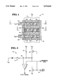
- FIG. 1 is a top view of a layout of a fuse structure according to one form of the present invention.
- FIG. 2 is a cross section of the fuse structure of FIG. 1 taken along line 2--2.
- FIG. 3 is a cross section of the fuse structure of FIG. 1 taken along line 3--3.
- FIG. 4 is a schematic of a circuit utilizing the fuse structure of FIG. 1.
- FIG. 1 shows a top layout view of a fuse structure 10 according to a preferred embodiment of the present invention.
- fuse structure 10 is but a single element on a much larger integrated circuit having perhaps many thousands of other elements including other similar fuse structures.
- the various circuit elements are connected to reference voltage potentials, such as V DD and V SS .
- a common arrangement is to have a first pattern of metal lines overlying but electrically insulated from the various circuit elements. This first pattern of metal lines is often referred to the metal 1 layer.
- a connection from a metal 1 line to a selected part of a circuit element is made by way of a "via".
- a better view of a via is shown in FIGS. 2 and 3, as will be described later.
- Metal 1 lines are generally at the same relative height above the chip substrate. Selected metal 1 lines are connected to a reference voltage potential, such as V SS . A second pattern of metal lines overlying but electrically insulated from the metal 1 layer is connected to a second reference voltage potential, such as V DD . This second pattern of metal lines is referred to a metal 2 and is selectively connected to underlying circuit elements by vias.
- the metal 1 layer includes metal runs 12a and 12b and a metal pad 12c.
- Metal runs 12a and 12b are connected to V SS .
- the metal 2 layer includes a metal run 14 which is connected to V DD .
- Metal run 14 is shown in outline only to reveal underlying features.
- a polysilicon pad 16 underlies metal 1 and metal 2 but overlies the substrate (not shown).
- the interconnections between metal runs 12a, 12b, metal pad 12c, metal run 14 and polysilicon pad 16 are made by a number of vias. Specifically, metal run 12a is connected to polysilicon pad 16 by vias 18a, 18b and 18c. Metal run 12b is connected to polysilicon pad 16 by vias 18d, 18e and 18f. Metal pad 12c is connected to polysilicon pad 16 by via 20, and is connected to metal run 14 by vias 22a and 22b.
- FIG. 2 is a cross sectional view taken along the line 2--2 in FIG. 1.
- a conventional chip base or substrate 24 with overlying oxide layer 26 is shown.
- Polysilicon pad 16 is formed on top of oxide layer 26.
- Metal run 12a overlies polysilicon pad 16 and is separated therefrom by oxide insulator 28.
- Vias 18a, 18b and 18c electrically connect metal run 12a to polysilicon pad 16.
- Metal run 14 is separated from metal run 12a by oxide insulator 30. It should be appreciated that a cross sectional view taken along metal run 12b in FIG. 1 would reveal a similar configuration to that shown in FIG. 2.
- FIG. 3 is a cross sectional view taken along the line 3--3 in FIG. 1.
- Metal pad 12c is separated from polysilicon pad 16 by oxide insulator 28 and from metal run 14 by oxide insulator 30.
- Metal pad 12c is also separated from metal runs 12a and 12b by an oxide insulator (not possible to show in FIG. 3 because runs 12a and 12b are in the same horizontal plane as pad 12c).
- the electrical connection between metal pad 12c and metal run 14 is provided by vias 22a and 22b.
- via 20 which forms the sole electrical connection between metal pad 12c and polysilicon pad 16.
- Via 20 is preferably aluminum and forms a fusible link at its intersection with polysilicon pad 16.
- the fuse is blown by driving a current from metal runs 12a and 12b through vias 18a-18f, into polysilicon pad 16, through via 20 into metal pad 12c and through vias 22a and 22b into metal run 14.
- the fusible link or via 20 will break at its intersection with polysilicon pad 20.
- fuse structure 10 Certain physical features of fuse structure 10 are particularly significant. First, is the choice of materials.
- the pad 16 material, polysilicon has a relatively high electrical resistance and melting point compared to the fusible link material, aluminum. Less current is required to heat polysilicon to the melting temperature of aluminum than the current required in an all aluminum fuse. Therefore, polysilicon pad 16 in the vicinity of via 20 is essentially a resistance heating element which provides the heat needed to melt the aluminum fusible link.
- polysilicon alloys or absorbs the melted aluminum. This helps prevent the aluminum from subsequently growing back.
- the current density is highest between via 20 (the fusible link) and polysilicon pad 16. This reduces the current needed to blow the fuse and assures that when the fuse is blown, the break will occur at the intersection of via 20 and polysilicon pad 16.
- the current required to blow the subject fuse is much less than that for conventional all metal fuses.
- the present fuse finds important application in a conventional CMOS process. (Bipolar transistors are not required to provide the programming current.)
- the choice of aluminum allows the subject fuse structure to be easily incorporated into a standard CMOS process. More complicated or expensive processes such as those involving tungsten deposition are also avoided.
- FIG. 4 is a schematic showing a circuit for a PROM cell 32 utilizing the fuse structure 10.
- a high of low voltage is applied to data input 34.
- a high voltage or "one” applied to input 34 turns on NMOS transistor 36, preventing current flow through fuse structure 10.
- fuse structure 10 pulls data storage node 36 low, keeping the value "stored” by node 36 as a "zero".
- PMOS transistor 38 is turned on thereby connecting V DD to V SS through fuse structure 10. The current driven therethrough is sufficient to blow the fuse.
- fuse structure 10 is an open circuit allowing storage node 36 to be maintained as a "one" at approximately the voltage of V DD through pullup resistor 40.
Abstract
Description
Claims (15)
Priority Applications (2)
| Application Number | Priority Date | Filing Date | Title |
|---|---|---|---|
| US07/832,177 US5376820A (en) | 1992-02-05 | 1992-02-05 | Semiconductor fuse structure |
| US08/839,426 US5759877A (en) | 1992-02-05 | 1997-04-14 | Semiconductor fuse structure |
Applications Claiming Priority (1)
| Application Number | Priority Date | Filing Date | Title |
|---|---|---|---|
| US07/832,177 US5376820A (en) | 1992-02-05 | 1992-02-05 | Semiconductor fuse structure |
Related Child Applications (1)
| Application Number | Title | Priority Date | Filing Date |
|---|---|---|---|
| US35197994A Division | 1992-02-05 | 1994-12-08 |
Publications (1)
| Publication Number | Publication Date |
|---|---|
| US5376820A true US5376820A (en) | 1994-12-27 |
Family
ID=25260909
Family Applications (2)
| Application Number | Title | Priority Date | Filing Date |
|---|---|---|---|
| US07/832,177 Expired - Lifetime US5376820A (en) | 1992-02-05 | 1992-02-05 | Semiconductor fuse structure |
| US08/839,426 Expired - Lifetime US5759877A (en) | 1992-02-05 | 1997-04-14 | Semiconductor fuse structure |
Family Applications After (1)
| Application Number | Title | Priority Date | Filing Date |
|---|---|---|---|
| US08/839,426 Expired - Lifetime US5759877A (en) | 1992-02-05 | 1997-04-14 | Semiconductor fuse structure |
Country Status (1)
| Country | Link |
|---|---|
| US (2) | US5376820A (en) |
Cited By (17)
| Publication number | Priority date | Publication date | Assignee | Title |
|---|---|---|---|---|
| US5949127A (en) * | 1997-06-06 | 1999-09-07 | Integrated Device Technology, Inc. | Electrically programmable interlevel fusible link for integrated circuits |
| US5976917A (en) * | 1998-01-29 | 1999-11-02 | Micron Technology, Inc. | Integrated circuitry fuse forming methods, integrated circuitry programming methods, and related integrated circuitry |
| US6013938A (en) * | 1996-07-19 | 2000-01-11 | Sharp Kabushiki Kaisha | Power control device |
| US6091273A (en) * | 1997-08-19 | 2000-07-18 | International Business Machines Corporation | Voltage limiting circuit for fuse technology |
| US6166421A (en) * | 1999-08-18 | 2000-12-26 | National Semiconductor Corporation | Polysilicon fuse that provides an open current path when programmed without exposing the fuse to the environment |
| US6218721B1 (en) * | 1997-01-14 | 2001-04-17 | Nec Corporation | Semiconductor device and method of manufacturing the same |
| US6252292B1 (en) * | 1999-06-09 | 2001-06-26 | International Business Machines Corporation | Vertical electrical cavity-fuse |
| US6703680B2 (en) * | 2001-12-04 | 2004-03-09 | Kabushiki Kaisha Toshiba | Programmable element programmed by changes in resistance due to phase transition |
| US20090078988A1 (en) * | 2007-09-21 | 2009-03-26 | Higuchi Yuichiro | Semiconductor device and method for manufacturing the same |
| US20100252908A1 (en) * | 2009-04-03 | 2010-10-07 | Freescale Semiconductor, Inc. | Electrically alterable circuit for use in an integrated circuit device |
| US20130049679A1 (en) * | 2010-04-08 | 2013-02-28 | Sony Chemical & Information Device Corporation | Protection element, battery control device, and battery pack |
| US20130140649A1 (en) * | 2011-12-01 | 2013-06-06 | John A. Rogers | Transient devices designed to undergo programmable transformations |
| US8633552B1 (en) | 2007-03-01 | 2014-01-21 | Micrel, Incorporated | ESD protection for MEMS resonator devices |
| US8666471B2 (en) | 2010-03-17 | 2014-03-04 | The Board Of Trustees Of The University Of Illinois | Implantable biomedical devices on bioresorbable substrates |
| WO2014169218A3 (en) * | 2013-04-12 | 2015-02-26 | The Board Of Trustees Of The University Of Illinois | Materials, electronic systems and modes for active and passive transience |
| US10292263B2 (en) | 2013-04-12 | 2019-05-14 | The Board Of Trustees Of The University Of Illinois | Biodegradable materials for multilayer transient printed circuit boards |
| US10925543B2 (en) | 2015-11-11 | 2021-02-23 | The Board Of Trustees Of The University Of Illinois | Bioresorbable silicon electronics for transient implants |
Families Citing this family (7)
| Publication number | Priority date | Publication date | Assignee | Title |
|---|---|---|---|---|
| US6323111B1 (en) | 1999-10-28 | 2001-11-27 | Agere Systems Guardian Corp | Preweakened on chip metal fuse using dielectric trenches for barrier layer isolation |
| US6344679B1 (en) | 1999-11-19 | 2002-02-05 | International Business Machines Corporation | Diode with alterable conductivity and method of making same |
| US6839873B1 (en) * | 2000-06-23 | 2005-01-04 | Cypress Semiconductor Corporation | Method and apparatus for programmable logic device (PLD) built-in-self-test (BIST) |
| KR100526474B1 (en) * | 2003-12-31 | 2005-11-08 | 동부아남반도체 주식회사 | Method for fabricating a semiconductor device |
| US7413980B2 (en) * | 2006-04-25 | 2008-08-19 | Texas Instruments Incorporated | Semiconductor device with improved contact fuse |
| US20080277756A1 (en) * | 2007-05-09 | 2008-11-13 | Freescale Semiconductor, Inc. | Electronic device and method for operating a memory circuit |
| US8101505B2 (en) * | 2008-06-09 | 2012-01-24 | International Business Machines Corporation | Programmable electrical fuse |
Citations (6)
| Publication number | Priority date | Publication date | Assignee | Title |
|---|---|---|---|---|
| US4045310A (en) * | 1976-05-03 | 1977-08-30 | Teletype Corporation | Starting product for the production of a read-only memory and a method of producing it and the read-only memory |
| JPS5966144A (en) * | 1982-10-08 | 1984-04-14 | Hitachi Micro Comput Eng Ltd | Fuse circuit for identification |
| US4651409A (en) * | 1984-02-09 | 1987-03-24 | Ncr Corporation | Method of fabricating a high density, low power, merged vertical fuse/bipolar transistor |
| US4692787A (en) * | 1980-05-23 | 1987-09-08 | Texas Instruments Incorporated | Programmable read-only-memory element with polycrystalline silicon layer |
| US4881114A (en) * | 1986-05-16 | 1989-11-14 | Actel Corporation | Selectively formable vertical diode circuit element |
| US5081064A (en) * | 1989-06-06 | 1992-01-14 | Fujitsu Limited | Method of forming electrical contact between interconnection layers located at different layer levels |
Family Cites Families (2)
| Publication number | Priority date | Publication date | Assignee | Title |
|---|---|---|---|---|
| JPS5685846A (en) * | 1979-12-14 | 1981-07-13 | Fujitsu Ltd | Semiconductor integrated circuit device |
| JPS6477141A (en) * | 1987-09-18 | 1989-03-23 | Fujitsu Ltd | Semiconductor device |
-
1992
- 1992-02-05 US US07/832,177 patent/US5376820A/en not_active Expired - Lifetime
-
1997
- 1997-04-14 US US08/839,426 patent/US5759877A/en not_active Expired - Lifetime
Patent Citations (6)
| Publication number | Priority date | Publication date | Assignee | Title |
|---|---|---|---|---|
| US4045310A (en) * | 1976-05-03 | 1977-08-30 | Teletype Corporation | Starting product for the production of a read-only memory and a method of producing it and the read-only memory |
| US4692787A (en) * | 1980-05-23 | 1987-09-08 | Texas Instruments Incorporated | Programmable read-only-memory element with polycrystalline silicon layer |
| JPS5966144A (en) * | 1982-10-08 | 1984-04-14 | Hitachi Micro Comput Eng Ltd | Fuse circuit for identification |
| US4651409A (en) * | 1984-02-09 | 1987-03-24 | Ncr Corporation | Method of fabricating a high density, low power, merged vertical fuse/bipolar transistor |
| US4881114A (en) * | 1986-05-16 | 1989-11-14 | Actel Corporation | Selectively formable vertical diode circuit element |
| US5081064A (en) * | 1989-06-06 | 1992-01-14 | Fujitsu Limited | Method of forming electrical contact between interconnection layers located at different layer levels |
Cited By (39)
| Publication number | Priority date | Publication date | Assignee | Title |
|---|---|---|---|---|
| US6013938A (en) * | 1996-07-19 | 2000-01-11 | Sharp Kabushiki Kaisha | Power control device |
| US6218721B1 (en) * | 1997-01-14 | 2001-04-17 | Nec Corporation | Semiconductor device and method of manufacturing the same |
| US5949127A (en) * | 1997-06-06 | 1999-09-07 | Integrated Device Technology, Inc. | Electrically programmable interlevel fusible link for integrated circuits |
| US6333524B1 (en) * | 1997-06-06 | 2001-12-25 | Integrated Device Technology, Inc. | Electrically programmable interlevel fusible link for integrated circuits |
| US6091273A (en) * | 1997-08-19 | 2000-07-18 | International Business Machines Corporation | Voltage limiting circuit for fuse technology |
| US6300170B1 (en) | 1998-01-29 | 2001-10-09 | Micron Technology, Inc. | Integrated circuitry fuse forming methods, integrated circuitry programming methods, and related integrated circuitry |
| US5976917A (en) * | 1998-01-29 | 1999-11-02 | Micron Technology, Inc. | Integrated circuitry fuse forming methods, integrated circuitry programming methods, and related integrated circuitry |
| US6249037B1 (en) * | 1998-01-29 | 2001-06-19 | Micron Technology, Inc. | Integrated circuitry fuse forming methods, integrated circuitry programming methods, and related integrated circuitry |
| US6265299B1 (en) | 1998-01-29 | 2001-07-24 | Micron Technology, Inc. | Integrated circuitry fuse forming methods, integrated circuitry programming methods, and related integrated circuitry |
| US6238955B1 (en) | 1998-01-29 | 2001-05-29 | Micron Technology, Inc. | Integrated circuitry fuse forming methods, integrated circuitry programming methods, and related integrated circuitry |
| US6680519B2 (en) | 1998-01-29 | 2004-01-20 | Micron Technology, Inc. | Integrated circuitry fuse forming methods, integrated circuitry programming methods, and related integrated circuitry |
| US6252292B1 (en) * | 1999-06-09 | 2001-06-26 | International Business Machines Corporation | Vertical electrical cavity-fuse |
| US6166421A (en) * | 1999-08-18 | 2000-12-26 | National Semiconductor Corporation | Polysilicon fuse that provides an open current path when programmed without exposing the fuse to the environment |
| US6703680B2 (en) * | 2001-12-04 | 2004-03-09 | Kabushiki Kaisha Toshiba | Programmable element programmed by changes in resistance due to phase transition |
| US8633552B1 (en) | 2007-03-01 | 2014-01-21 | Micrel, Incorporated | ESD protection for MEMS resonator devices |
| US9266722B2 (en) | 2007-03-01 | 2016-02-23 | Micrel, Incorporated | ESD protection for MEMS resonator devices |
| US7821100B2 (en) * | 2007-09-21 | 2010-10-26 | Panasonic Corporation | Semiconductor device and method for manufacturing the same |
| US20090078988A1 (en) * | 2007-09-21 | 2009-03-26 | Higuchi Yuichiro | Semiconductor device and method for manufacturing the same |
| US20100252908A1 (en) * | 2009-04-03 | 2010-10-07 | Freescale Semiconductor, Inc. | Electrically alterable circuit for use in an integrated circuit device |
| US8178942B2 (en) | 2009-04-03 | 2012-05-15 | Freescale Semiconductor, Inc. | Electrically alterable circuit for use in an integrated circuit device |
| US9986924B2 (en) | 2010-03-17 | 2018-06-05 | The Board Of Trustees Of The University Of Illinois | Implantable biomedical devices on bioresorbable substrates |
| US8666471B2 (en) | 2010-03-17 | 2014-03-04 | The Board Of Trustees Of The University Of Illinois | Implantable biomedical devices on bioresorbable substrates |
| US20130049679A1 (en) * | 2010-04-08 | 2013-02-28 | Sony Chemical & Information Device Corporation | Protection element, battery control device, and battery pack |
| US9184609B2 (en) * | 2010-04-08 | 2015-11-10 | Dexerials Corporation | Overcurrent and overvoltage protecting fuse for battery pack with electrodes on either side of an insulated substrate connected by through-holes |
| US9691873B2 (en) * | 2011-12-01 | 2017-06-27 | The Board Of Trustees Of The University Of Illinois | Transient devices designed to undergo programmable transformations |
| JP2018032870A (en) * | 2011-12-01 | 2018-03-01 | ザ ボード オブ トラスティーズ オブ ザ ユニヴァーシティー オブ イリノイ | Transition device designed to be subject to programmable change |
| CN104472023A (en) * | 2011-12-01 | 2015-03-25 | 伊利诺伊大学评议会 | Transient devices designed to undergo programmable transformations |
| JP2015512136A (en) * | 2011-12-01 | 2015-04-23 | ザ ボード オブ トラスティーズ オブ ザ ユニヴァーシティー オブ イリノイ | Transition devices designed to undergo programmable changes |
| EP2786644A4 (en) * | 2011-12-01 | 2015-09-02 | Univ Illinois | Transient devices designed to undergo programmable transformations |
| KR20140099934A (en) * | 2011-12-01 | 2014-08-13 | 더 보오드 오브 트러스티스 오브 더 유니버시티 오브 일리노이즈 | Transient devices designed to undergo programmable transformations |
| US10396173B2 (en) | 2011-12-01 | 2019-08-27 | The Board Of Trustees Of The University Of Illinois | Transient devices designed to undergo programmable transformations |
| WO2013089867A3 (en) * | 2011-12-01 | 2013-08-15 | The Board Of Trustees Of The University Of Illinois | Transient devices designed to undergo programmable transformations |
| WO2013089867A2 (en) | 2011-12-01 | 2013-06-20 | The Board Of Trustees Of The University Of Illinois | Transient devices designed to undergo programmable transformations |
| US20130140649A1 (en) * | 2011-12-01 | 2013-06-06 | John A. Rogers | Transient devices designed to undergo programmable transformations |
| CN108389893A (en) * | 2011-12-01 | 2018-08-10 | 伊利诺伊大学评议会 | It is designed to undergo the transient state device of programmable transformation |
| US10154592B2 (en) | 2013-04-12 | 2018-12-11 | The Board Of Trustees Of The University Of Illinois | Materials, electronic systems and modes for active and passive transience |
| US10292263B2 (en) | 2013-04-12 | 2019-05-14 | The Board Of Trustees Of The University Of Illinois | Biodegradable materials for multilayer transient printed circuit boards |
| WO2014169218A3 (en) * | 2013-04-12 | 2015-02-26 | The Board Of Trustees Of The University Of Illinois | Materials, electronic systems and modes for active and passive transience |
| US10925543B2 (en) | 2015-11-11 | 2021-02-23 | The Board Of Trustees Of The University Of Illinois | Bioresorbable silicon electronics for transient implants |
Also Published As
| Publication number | Publication date |
|---|---|
| US5759877A (en) | 1998-06-02 |
Similar Documents
| Publication | Publication Date | Title |
|---|---|---|
| US5376820A (en) | Semiconductor fuse structure | |
| US5536968A (en) | Polysilicon fuse array structure for integrated circuits | |
| US5420456A (en) | ZAG fuse for reduced blow-current application | |
| US5301143A (en) | Method for identifying a semiconductor die using an IC with programmable links | |
| JP3537899B2 (en) | Reprogrammable electric circuit and connection changing method for enabling reprogrammability | |
| US5311053A (en) | Interconnection network | |
| US7572724B2 (en) | Doped single crystal silicon silicided eFuse | |
| US5427979A (en) | Method for making multi-level antifuse structure | |
| US8575718B2 (en) | Programmable electrical fuse | |
| JP3470960B2 (en) | Mixed fuse technology | |
| US6913954B2 (en) | Programmable fuse device | |
| US8232190B2 (en) | Three dimensional vertical E-fuse structures and methods of manufacturing the same | |
| EP0323078A3 (en) | Electrically-programmable low-impedance anti-fuse element | |
| US8796739B2 (en) | Ballasted polycrystalline fuse | |
| TW200834893A (en) | Mask programmable anti-fuse architecture | |
| US20100117190A1 (en) | Fuse structure for intergrated circuit devices | |
| US7667289B2 (en) | Fuse structure having a tortuous metal fuse line | |
| JPS6344757A (en) | Semiconductor device | |
| TWI303480B (en) | Mixed implantation on polysilicon fuse for cmos technology | |
| JP2010267803A (en) | Semiconductor device | |
| US20080203555A1 (en) | Universal substrate and semiconductor device utilizing the substrate | |
| US5949127A (en) | Electrically programmable interlevel fusible link for integrated circuits | |
| US20030094671A1 (en) | Antifuses | |
| JPH0451563A (en) | Semiconductor device | |
| JPH04242959A (en) | Cell structure of integrated circuit |
Legal Events
| Date | Code | Title | Description |
|---|---|---|---|
| AS | Assignment |
Owner name: NCR CORPORATION, OHIO Free format text: ASSIGNMENT OF ASSIGNORS INTEREST.;ASSIGNORS:CRAFTS, HAROLD S.;MCKINLEY, WILLIAM W.;SCAGGS, MARK O.;REEL/FRAME:006006/0236;SIGNING DATES FROM 19920109 TO 19920119 |
|
| STCF | Information on status: patent grant |
Free format text: PATENTED CASE |
|
| AS | Assignment |
Owner name: HYUNDAI ELECTRONICS AMERICA Free format text: ASSIGNMENT OF ASSIGNORS INTEREST;ASSIGNOR:AT&T GLOBAL INFORMATION SOLUTIONS COMPANY (FORMERLY KNOWN AS NCR CORPORATION);REEL/FRAME:007408/0104 Effective date: 19950215 |
|
| AS | Assignment |
Owner name: SYMBIOS LOGIC INC., COLORADO Free format text: ASSIGNMENT OF ASSIGNORS INTEREST;ASSIGNOR:HYUNDAI ELECTRONICS AMERICA;REEL/FRAME:007629/0431 Effective date: 19950818 |
|
| FEPP | Fee payment procedure |
Free format text: PAYOR NUMBER ASSIGNED (ORIGINAL EVENT CODE: ASPN); ENTITY STATUS OF PATENT OWNER: LARGE ENTITY |
|
| AS | Assignment |
Owner name: SYMBIOS, INC ., COLORADO Free format text: CHANGE OF NAME;ASSIGNOR:SYMBIOS LOGIC INC.;REEL/FRAME:009089/0936 Effective date: 19971210 |
|
| FPAY | Fee payment |
Year of fee payment: 4 |
|
| AS | Assignment |
Owner name: LEHMAN COMMERCIAL PAPER INC., AS ADMINISTRATIVE AG Free format text: SECURITY AGREEMENT;ASSIGNORS:HYUNDAI ELECTRONICS AMERICA, A CORP. OF CALIFORNIA;SYMBIOS, INC., A CORP. OF DELAWARE;REEL/FRAME:009396/0441 Effective date: 19980226 |
|
| AS | Assignment |
Owner name: HYUNDAI ELECTRONICS AMERICA, CALIFORNIA Free format text: TERMINATION AND LICENSE AGREEMENT;ASSIGNOR:SYMBIOS, INC.;REEL/FRAME:009596/0539 Effective date: 19980806 |
|
| FPAY | Fee payment |
Year of fee payment: 8 |
|
| REMI | Maintenance fee reminder mailed | ||
| AS | Assignment |
Owner name: HYNIX SEMICONDUCTOR AMERICA INC., CALIFORNIA Free format text: CHANGE OF NAME;ASSIGNOR:HYUNDAI ELECTRONICS AMERICA;REEL/FRAME:015246/0599 Effective date: 20010412 Owner name: HYNIX SEMICONDUCTOR INC., KOREA, REPUBLIC OF Free format text: ASSIGNMENT OF ASSIGNORS INTEREST;ASSIGNOR:HYNIX SEMICONDUCTOR AMERICA, INC.;REEL/FRAME:015279/0556 Effective date: 20040920 |
|
| AS | Assignment |
Owner name: MAGNACHIP SEMICONDUCTOR, LTD., KOREA, REPUBLIC OF Free format text: ASSIGNMENT OF ASSIGNORS INTEREST;ASSIGNOR:HYNIX SEMICONDUCTOR, INC.;REEL/FRAME:016216/0649 Effective date: 20041004 |
|
| AS | Assignment |
Owner name: U.S. BANK NATIONAL ASSOCIATION, AS COLLATERAL TRUS Free format text: SECURITY INTEREST;ASSIGNOR:MAGNACHIP SEMICONDUCTOR, LTD.;REEL/FRAME:016470/0530 Effective date: 20041223 |
|
| AS | Assignment |
Owner name: SYMBIOS, INC., COLORADO Free format text: RELEASE OF SECURITY INTEREST;ASSIGNOR:LEHMAN COMMERICAL PAPER INC.;REEL/FRAME:016602/0895 Effective date: 20050107 Owner name: HYUNDAI ELECTRONICS AMERICA, CALIFORNIA Free format text: RELEASE OF SECURITY INTEREST;ASSIGNOR:LEHMAN COMMERICAL PAPER INC.;REEL/FRAME:016602/0895 Effective date: 20050107 |
|
| FPAY | Fee payment |
Year of fee payment: 12 |
|
| AS | Assignment |
Owner name: MAGNACHIP SEMICONDUCTOR LTD.,KOREA, DEMOCRATIC PEO Free format text: RELEASE BY SECURED PARTY;ASSIGNOR:U.S. BANK NATIONAL ASSOCIATION;REEL/FRAME:024563/0807 Effective date: 20100527 |
|
| AS | Assignment |
Owner name: MAGNACHIP SEMICONDUCTOR LTD., KOREA, REPUBLIC OF Free format text: CORRECTIVE ASSIGNMENT TO CORRECT THE RECEIVING PARTY ADDRESS PREVIOUSLY RECORDED AT REEL: 024563 FRAME: 0807. ASSIGNOR(S) HEREBY CONFIRMS THE RELEASE BY SECURED PARTY;ASSIGNOR:US BANK NATIONAL ASSOCIATION;REEL/FRAME:034469/0001 Effective date: 20100527 |