US5391510A - Formation of self-aligned metal gate FETs using a benignant removable gate material during high temperature steps - Google Patents
Formation of self-aligned metal gate FETs using a benignant removable gate material during high temperature steps Download PDFInfo
- Publication number
- US5391510A US5391510A US08/225,360 US22536094A US5391510A US 5391510 A US5391510 A US 5391510A US 22536094 A US22536094 A US 22536094A US 5391510 A US5391510 A US 5391510A
- Authority
- US
- United States
- Prior art keywords
- gate
- self
- high temperature
- annealing
- metal
- Prior art date
- Legal status (The legal status is an assumption and is not a legal conclusion. Google has not performed a legal analysis and makes no representation as to the accuracy of the status listed.)
- Expired - Fee Related
Links
- 229910052751 metal Inorganic materials 0.000 title claims abstract description 28
- 239000002184 metal Substances 0.000 title claims abstract description 28
- 239000000463 material Substances 0.000 title claims abstract description 13
- 230000015572 biosynthetic process Effects 0.000 title description 5
- 238000000137 annealing Methods 0.000 claims abstract description 18
- 238000000034 method Methods 0.000 claims abstract description 15
- 229910052799 carbon Inorganic materials 0.000 claims abstract description 4
- 239000000758 substrate Substances 0.000 claims description 7
- 239000004065 semiconductor Substances 0.000 claims description 4
- 230000000873 masking effect Effects 0.000 claims 5
- 238000011109 contamination Methods 0.000 abstract description 5
- 238000005468 ion implantation Methods 0.000 abstract description 3
- 238000010899 nucleation Methods 0.000 description 7
- 238000004519 manufacturing process Methods 0.000 description 6
- 125000006850 spacer group Chemical group 0.000 description 6
- XUIMIQQOPSSXEZ-UHFFFAOYSA-N Silicon Chemical compound [Si] XUIMIQQOPSSXEZ-UHFFFAOYSA-N 0.000 description 5
- 210000002381 plasma Anatomy 0.000 description 5
- 229910052710 silicon Inorganic materials 0.000 description 5
- 239000010703 silicon Substances 0.000 description 5
- 238000000151 deposition Methods 0.000 description 4
- 230000008021 deposition Effects 0.000 description 4
- 230000035515 penetration Effects 0.000 description 4
- 229910003460 diamond Inorganic materials 0.000 description 3
- 239000010432 diamond Substances 0.000 description 3
- 238000005530 etching Methods 0.000 description 3
- 150000002500 ions Chemical class 0.000 description 3
- 238000001020 plasma etching Methods 0.000 description 3
- 238000012545 processing Methods 0.000 description 3
- WFKWXMTUELFFGS-UHFFFAOYSA-N tungsten Chemical compound [W] WFKWXMTUELFFGS-UHFFFAOYSA-N 0.000 description 3
- 229910052721 tungsten Inorganic materials 0.000 description 3
- 239000010937 tungsten Substances 0.000 description 3
- ZOKXTWBITQBERF-UHFFFAOYSA-N Molybdenum Chemical compound [Mo] ZOKXTWBITQBERF-UHFFFAOYSA-N 0.000 description 2
- 229910021417 amorphous silicon Inorganic materials 0.000 description 2
- 238000007796 conventional method Methods 0.000 description 2
- 238000013461 design Methods 0.000 description 2
- 239000003989 dielectric material Substances 0.000 description 2
- 239000007943 implant Substances 0.000 description 2
- 238000002513 implantation Methods 0.000 description 2
- 238000002955 isolation Methods 0.000 description 2
- 238000012986 modification Methods 0.000 description 2
- 230000004048 modification Effects 0.000 description 2
- 229910052750 molybdenum Inorganic materials 0.000 description 2
- 239000011733 molybdenum Substances 0.000 description 2
- 150000004767 nitrides Chemical class 0.000 description 2
- 229910021420 polycrystalline silicon Inorganic materials 0.000 description 2
- 229920005591 polysilicon Polymers 0.000 description 2
- 239000000126 substance Substances 0.000 description 2
- OKTJSMMVPCPJKN-UHFFFAOYSA-N Carbon Chemical compound [C] OKTJSMMVPCPJKN-UHFFFAOYSA-N 0.000 description 1
- 239000004215 Carbon black (E152) Substances 0.000 description 1
- ATJFFYVFTNAWJD-UHFFFAOYSA-N Tin Chemical compound [Sn] ATJFFYVFTNAWJD-UHFFFAOYSA-N 0.000 description 1
- 230000006978 adaptation Effects 0.000 description 1
- 229910052782 aluminium Inorganic materials 0.000 description 1
- XAGFODPZIPBFFR-UHFFFAOYSA-N aluminium Chemical compound [Al] XAGFODPZIPBFFR-UHFFFAOYSA-N 0.000 description 1
- 239000000356 contaminant Substances 0.000 description 1
- 230000006866 deterioration Effects 0.000 description 1
- 230000000694 effects Effects 0.000 description 1
- 230000005669 field effect Effects 0.000 description 1
- 229910052732 germanium Inorganic materials 0.000 description 1
- GNPVGFCGXDBREM-UHFFFAOYSA-N germanium atom Chemical compound [Ge] GNPVGFCGXDBREM-UHFFFAOYSA-N 0.000 description 1
- PCHJSUWPFVWCPO-UHFFFAOYSA-N gold Chemical compound [Au] PCHJSUWPFVWCPO-UHFFFAOYSA-N 0.000 description 1
- 229910052737 gold Inorganic materials 0.000 description 1
- 239000010931 gold Substances 0.000 description 1
- 229930195733 hydrocarbon Natural products 0.000 description 1
- 150000002430 hydrocarbons Chemical class 0.000 description 1
- 239000012212 insulator Substances 0.000 description 1
- 238000000623 plasma-assisted chemical vapour deposition Methods 0.000 description 1
- 238000005498 polishing Methods 0.000 description 1
- 239000002243 precursor Substances 0.000 description 1
- 229910021332 silicide Inorganic materials 0.000 description 1
- FVBUAEGBCNSCDD-UHFFFAOYSA-N silicide(4-) Chemical compound [Si-4] FVBUAEGBCNSCDD-UHFFFAOYSA-N 0.000 description 1
- -1 silicon: 32E-7/C Chemical compound 0.000 description 1
- WQJQOUPTWCFRMM-UHFFFAOYSA-N tungsten disilicide Chemical compound [Si]#[W]#[Si] WQJQOUPTWCFRMM-UHFFFAOYSA-N 0.000 description 1
- 229910021342 tungsten silicide Inorganic materials 0.000 description 1
Images


Classifications
-
- H—ELECTRICITY
- H01—ELECTRIC ELEMENTS
- H01L—SEMICONDUCTOR DEVICES NOT COVERED BY CLASS H10
- H01L29/00—Semiconductor devices adapted for rectifying, amplifying, oscillating or switching, or capacitors or resistors with at least one potential-jump barrier or surface barrier, e.g. PN junction depletion layer or carrier concentration layer; Details of semiconductor bodies or of electrodes thereof ; Multistep manufacturing processes therefor
- H01L29/66—Types of semiconductor device ; Multistep manufacturing processes therefor
- H01L29/66007—Multistep manufacturing processes
- H01L29/66075—Multistep manufacturing processes of devices having semiconductor bodies comprising group 14 or group 13/15 materials
- H01L29/66227—Multistep manufacturing processes of devices having semiconductor bodies comprising group 14 or group 13/15 materials the devices being controllable only by the electric current supplied or the electric potential applied, to an electrode which does not carry the current to be rectified, amplified or switched, e.g. three-terminal devices
- H01L29/66409—Unipolar field-effect transistors
- H01L29/66477—Unipolar field-effect transistors with an insulated gate, i.e. MISFET
- H01L29/66568—Lateral single gate silicon transistors
- H01L29/66575—Lateral single gate silicon transistors where the source and drain or source and drain extensions are self-aligned to the sides of the gate
- H01L29/6659—Lateral single gate silicon transistors where the source and drain or source and drain extensions are self-aligned to the sides of the gate with both lightly doped source and drain extensions and source and drain self-aligned to the sides of the gate, e.g. lightly doped drain [LDD] MOSFET, double diffused drain [DDD] MOSFET
-
- H—ELECTRICITY
- H01—ELECTRIC ELEMENTS
- H01L—SEMICONDUCTOR DEVICES NOT COVERED BY CLASS H10
- H01L21/00—Processes or apparatus adapted for the manufacture or treatment of semiconductor or solid state devices or of parts thereof
- H01L21/02—Manufacture or treatment of semiconductor devices or of parts thereof
- H01L21/04—Manufacture or treatment of semiconductor devices or of parts thereof the devices having at least one potential-jump barrier or surface barrier, e.g. PN junction, depletion layer or carrier concentration layer
- H01L21/18—Manufacture or treatment of semiconductor devices or of parts thereof the devices having at least one potential-jump barrier or surface barrier, e.g. PN junction, depletion layer or carrier concentration layer the devices having semiconductor bodies comprising elements of Group IV of the Periodic System or AIIIBV compounds with or without impurities, e.g. doping materials
- H01L21/28—Manufacture of electrodes on semiconductor bodies using processes or apparatus not provided for in groups H01L21/20 - H01L21/268
- H01L21/28008—Making conductor-insulator-semiconductor electrodes
- H01L21/28017—Making conductor-insulator-semiconductor electrodes the insulator being formed after the semiconductor body, the semiconductor being silicon
- H01L21/28026—Making conductor-insulator-semiconductor electrodes the insulator being formed after the semiconductor body, the semiconductor being silicon characterised by the conductor
- H01L21/28079—Making conductor-insulator-semiconductor electrodes the insulator being formed after the semiconductor body, the semiconductor being silicon characterised by the conductor the final conductor layer next to the insulator being a single metal, e.g. Ta, W, Mo, Al
-
- H—ELECTRICITY
- H01—ELECTRIC ELEMENTS
- H01L—SEMICONDUCTOR DEVICES NOT COVERED BY CLASS H10
- H01L21/00—Processes or apparatus adapted for the manufacture or treatment of semiconductor or solid state devices or of parts thereof
- H01L21/02—Manufacture or treatment of semiconductor devices or of parts thereof
- H01L21/04—Manufacture or treatment of semiconductor devices or of parts thereof the devices having at least one potential-jump barrier or surface barrier, e.g. PN junction, depletion layer or carrier concentration layer
- H01L21/18—Manufacture or treatment of semiconductor devices or of parts thereof the devices having at least one potential-jump barrier or surface barrier, e.g. PN junction, depletion layer or carrier concentration layer the devices having semiconductor bodies comprising elements of Group IV of the Periodic System or AIIIBV compounds with or without impurities, e.g. doping materials
- H01L21/28—Manufacture of electrodes on semiconductor bodies using processes or apparatus not provided for in groups H01L21/20 - H01L21/268
- H01L21/28008—Making conductor-insulator-semiconductor electrodes
- H01L21/28017—Making conductor-insulator-semiconductor electrodes the insulator being formed after the semiconductor body, the semiconductor being silicon
- H01L21/28026—Making conductor-insulator-semiconductor electrodes the insulator being formed after the semiconductor body, the semiconductor being silicon characterised by the conductor
- H01L21/28114—Making conductor-insulator-semiconductor electrodes the insulator being formed after the semiconductor body, the semiconductor being silicon characterised by the conductor characterised by the sectional shape, e.g. T, inverted-T
-
- H—ELECTRICITY
- H01—ELECTRIC ELEMENTS
- H01L—SEMICONDUCTOR DEVICES NOT COVERED BY CLASS H10
- H01L21/00—Processes or apparatus adapted for the manufacture or treatment of semiconductor or solid state devices or of parts thereof
- H01L21/02—Manufacture or treatment of semiconductor devices or of parts thereof
- H01L21/04—Manufacture or treatment of semiconductor devices or of parts thereof the devices having at least one potential-jump barrier or surface barrier, e.g. PN junction, depletion layer or carrier concentration layer
- H01L21/18—Manufacture or treatment of semiconductor devices or of parts thereof the devices having at least one potential-jump barrier or surface barrier, e.g. PN junction, depletion layer or carrier concentration layer the devices having semiconductor bodies comprising elements of Group IV of the Periodic System or AIIIBV compounds with or without impurities, e.g. doping materials
- H01L21/28—Manufacture of electrodes on semiconductor bodies using processes or apparatus not provided for in groups H01L21/20 - H01L21/268
- H01L21/28008—Making conductor-insulator-semiconductor electrodes
- H01L21/28017—Making conductor-insulator-semiconductor electrodes the insulator being formed after the semiconductor body, the semiconductor being silicon
- H01L21/28026—Making conductor-insulator-semiconductor electrodes the insulator being formed after the semiconductor body, the semiconductor being silicon characterised by the conductor
- H01L21/28123—Lithography-related aspects, e.g. sub-lithography lengths; Isolation-related aspects, e.g. to solve problems arising at the crossing with the side of the device isolation; Planarisation aspects
- H01L21/28132—Lithography-related aspects, e.g. sub-lithography lengths; Isolation-related aspects, e.g. to solve problems arising at the crossing with the side of the device isolation; Planarisation aspects conducting part of electrode is difined by a sidewall spacer or a similar technique, e.g. oxidation under mask, plating
-
- H—ELECTRICITY
- H01—ELECTRIC ELEMENTS
- H01L—SEMICONDUCTOR DEVICES NOT COVERED BY CLASS H10
- H01L21/00—Processes or apparatus adapted for the manufacture or treatment of semiconductor or solid state devices or of parts thereof
- H01L21/02—Manufacture or treatment of semiconductor devices or of parts thereof
- H01L21/04—Manufacture or treatment of semiconductor devices or of parts thereof the devices having at least one potential-jump barrier or surface barrier, e.g. PN junction, depletion layer or carrier concentration layer
- H01L21/18—Manufacture or treatment of semiconductor devices or of parts thereof the devices having at least one potential-jump barrier or surface barrier, e.g. PN junction, depletion layer or carrier concentration layer the devices having semiconductor bodies comprising elements of Group IV of the Periodic System or AIIIBV compounds with or without impurities, e.g. doping materials
- H01L21/28—Manufacture of electrodes on semiconductor bodies using processes or apparatus not provided for in groups H01L21/20 - H01L21/268
- H01L21/28008—Making conductor-insulator-semiconductor electrodes
- H01L21/28017—Making conductor-insulator-semiconductor electrodes the insulator being formed after the semiconductor body, the semiconductor being silicon
- H01L21/28026—Making conductor-insulator-semiconductor electrodes the insulator being formed after the semiconductor body, the semiconductor being silicon characterised by the conductor
- H01L21/28123—Lithography-related aspects, e.g. sub-lithography lengths; Isolation-related aspects, e.g. to solve problems arising at the crossing with the side of the device isolation; Planarisation aspects
- H01L21/28141—Lithography-related aspects, e.g. sub-lithography lengths; Isolation-related aspects, e.g. to solve problems arising at the crossing with the side of the device isolation; Planarisation aspects insulating part of the electrode is defined by a sidewall spacer, e.g. dummy spacer, or a similar technique, e.g. oxidation under mask, plating
-
- H—ELECTRICITY
- H01—ELECTRIC ELEMENTS
- H01L—SEMICONDUCTOR DEVICES NOT COVERED BY CLASS H10
- H01L29/00—Semiconductor devices adapted for rectifying, amplifying, oscillating or switching, or capacitors or resistors with at least one potential-jump barrier or surface barrier, e.g. PN junction depletion layer or carrier concentration layer; Details of semiconductor bodies or of electrodes thereof ; Multistep manufacturing processes therefor
- H01L29/40—Electrodes ; Multistep manufacturing processes therefor
- H01L29/41—Electrodes ; Multistep manufacturing processes therefor characterised by their shape, relative sizes or dispositions
- H01L29/423—Electrodes ; Multistep manufacturing processes therefor characterised by their shape, relative sizes or dispositions not carrying the current to be rectified, amplified or switched
- H01L29/42312—Gate electrodes for field effect devices
- H01L29/42316—Gate electrodes for field effect devices for field-effect transistors
-
- H—ELECTRICITY
- H01—ELECTRIC ELEMENTS
- H01L—SEMICONDUCTOR DEVICES NOT COVERED BY CLASS H10
- H01L29/00—Semiconductor devices adapted for rectifying, amplifying, oscillating or switching, or capacitors or resistors with at least one potential-jump barrier or surface barrier, e.g. PN junction depletion layer or carrier concentration layer; Details of semiconductor bodies or of electrodes thereof ; Multistep manufacturing processes therefor
- H01L29/40—Electrodes ; Multistep manufacturing processes therefor
- H01L29/43—Electrodes ; Multistep manufacturing processes therefor characterised by the materials of which they are formed
- H01L29/47—Schottky barrier electrodes
-
- H—ELECTRICITY
- H01—ELECTRIC ELEMENTS
- H01L—SEMICONDUCTOR DEVICES NOT COVERED BY CLASS H10
- H01L29/00—Semiconductor devices adapted for rectifying, amplifying, oscillating or switching, or capacitors or resistors with at least one potential-jump barrier or surface barrier, e.g. PN junction depletion layer or carrier concentration layer; Details of semiconductor bodies or of electrodes thereof ; Multistep manufacturing processes therefor
- H01L29/66—Types of semiconductor device ; Multistep manufacturing processes therefor
- H01L29/66007—Multistep manufacturing processes
- H01L29/66075—Multistep manufacturing processes of devices having semiconductor bodies comprising group 14 or group 13/15 materials
- H01L29/66227—Multistep manufacturing processes of devices having semiconductor bodies comprising group 14 or group 13/15 materials the devices being controllable only by the electric current supplied or the electric potential applied, to an electrode which does not carry the current to be rectified, amplified or switched, e.g. three-terminal devices
- H01L29/66409—Unipolar field-effect transistors
- H01L29/66477—Unipolar field-effect transistors with an insulated gate, i.e. MISFET
- H01L29/66545—Unipolar field-effect transistors with an insulated gate, i.e. MISFET using a dummy, i.e. replacement gate in a process wherein at least a part of the final gate is self aligned to the dummy gate
-
- H—ELECTRICITY
- H01—ELECTRIC ELEMENTS
- H01L—SEMICONDUCTOR DEVICES NOT COVERED BY CLASS H10
- H01L29/00—Semiconductor devices adapted for rectifying, amplifying, oscillating or switching, or capacitors or resistors with at least one potential-jump barrier or surface barrier, e.g. PN junction depletion layer or carrier concentration layer; Details of semiconductor bodies or of electrodes thereof ; Multistep manufacturing processes therefor
- H01L29/66—Types of semiconductor device ; Multistep manufacturing processes therefor
- H01L29/66007—Multistep manufacturing processes
- H01L29/66075—Multistep manufacturing processes of devices having semiconductor bodies comprising group 14 or group 13/15 materials
- H01L29/66227—Multistep manufacturing processes of devices having semiconductor bodies comprising group 14 or group 13/15 materials the devices being controllable only by the electric current supplied or the electric potential applied, to an electrode which does not carry the current to be rectified, amplified or switched, e.g. three-terminal devices
- H01L29/66409—Unipolar field-effect transistors
- H01L29/66477—Unipolar field-effect transistors with an insulated gate, i.e. MISFET
- H01L29/66568—Lateral single gate silicon transistors
- H01L29/66659—Lateral single gate silicon transistors with asymmetry in the channel direction, e.g. lateral high-voltage MISFETs with drain offset region, extended drain MISFETs
-
- Y—GENERAL TAGGING OF NEW TECHNOLOGICAL DEVELOPMENTS; GENERAL TAGGING OF CROSS-SECTIONAL TECHNOLOGIES SPANNING OVER SEVERAL SECTIONS OF THE IPC; TECHNICAL SUBJECTS COVERED BY FORMER USPC CROSS-REFERENCE ART COLLECTIONS [XRACs] AND DIGESTS
- Y10—TECHNICAL SUBJECTS COVERED BY FORMER USPC
- Y10S—TECHNICAL SUBJECTS COVERED BY FORMER USPC CROSS-REFERENCE ART COLLECTIONS [XRACs] AND DIGESTS
- Y10S438/00—Semiconductor device manufacturing: process
- Y10S438/942—Masking
- Y10S438/945—Special, e.g. metal
Definitions
- the invention generally relates to field effect transistors of the self-aligned metal gate type and, more particularly, to a method of fabricating same that avoids certain problems associated with high temperature processing steps.
- Metal gates have been used to improve gate conductivity in high density self-aligned FET devices. Such use, however, can encounter significant difficulties, e.g., the penetration of the gate metal into the gate oxide (if the metal gate is present during high temperature fabrication steps) as well as otherwise damaging the gate oxide during the gate formation steps. These and other problems become intensified when the FET devices are reduced to the submicron range. Not only must the gate oxide be protected during the aforementioned processing steps, but that objective must be accomplished in a manner consistent with self-alignment techniques in order to achieve close dimensional control for high device density chip designs where there is a desire to avoid the need for advanced lithographic tools.
- a metal gate is added after the annealing step is completed. Although the gate metal penetration problem alluded to above is avoided in the last two cited references, the gate oxide is left uncovered in both cases during the high temperature annealing step, exposing said oxide to latent contaminants present within the annealing furnace.
- One object of the present invention is to provide self-aligned metal gate FETs having substantially no gate metal or other contamination of the gate insulator attributable to annealing steps.
- Another object is to provide a method for making self-aligned metal gate FETs whereby the gate dielectric is protected during annealing steps by a high temperature-stable, inert and easily removable material.
- a further object is to provide a method for making sub-micron self-aligned metal gate FETs whereby the gate dielectric is covered during annealing steps by a relatively thin seeding layer of the final gate metal and an overlying relatively thick layer of a high temperature-stable, inert and easily removable material.
- an FET gate structure which is self-aligned relative to the source and drain regions and is expended after the source and drain have been annealed.
- a diamond-like-carbon (DLC) material preferably is used as the expendable gate structure to protect the gate dielectric layer from contamination during high temperature annealing.
- the DLC material is replaced by a metal gate electrode to complete the FET gate structure.
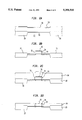
- FIGS. 1a-1L are a series of simplified cross-sectional views Of a portion of a semiconductor chip as it appears at a succession of times during the fabrication of a first embodiment of the present invention especially adapted for sub-micron FETs, and
- FIGS. 2a-2h are a series of simplified cross-sectional views of a portion of a semiconductor chip as it appears at a succession of times during the fabrication of a second embodiment of the present invention omitting special adaptation for very small sized FETs.
- fully recessed oxide isolation regions 1, 2 and 3 are produced in a conventional manner on silicon substrate 4.
- conventional channel stop implants beneath the oxide regions
- threshold adjust implants in the device areas between the oxide regions
- about 250 ⁇ of pad oxide 5 is grown.
- CVD polysilicon or amorphous Si 6 is deposited, photolithographed and patterned preferably by reactive ion etching to yield the structure shown in FIG. 1b.
- Pad oxide 5 now is stripped and replaced by about 100 ⁇ of regrown gate oxide 7 (FIG. 1c).
- a gate metal seeding layer such as about 250 ⁇ of tungsten silicide 8 is deposited on the entire surface of the structure including gate oxide 7 as depicted in FIG. 1d.
- TiN may be used as seeding material for later deposited CVD tungsten as described in U.S. Pat. No. 4,822,753 issued to Faivel Pintchovski et al on Apr. 18, 1989.
- a CVD diamond-like carbon layer is deposited (FIG. 1e).
- the thickness of layer 9 is equivalent to the designated gate length, e.g., 2000 ⁇ or less.
- the use of the DLC layer 9 is an important aspect of the present invention.
- the deposited DLC film has good thermal and chemical stability even at high annealing temperatures and easily can be removed later with an O 2 /Ar plasma without damaging the underlying seed layer 8 or gate oxide 7.
- a suitable etching process is described in the paper Reactive Ion Etching of Diamond by G. S. Sandu et al, Journal Appl. Phys. Lett. Vol. 55, No. 5, 1989, p. 437.
- the thermal and chemical stability of DLC 9 furthermore, fully protects the gate oxide from ambient contamination during high temperature processing steps without introducing film stress as in other cases where metal gates are in place as reported in the paper Effect of W Film on W Gate MOS Characteristics by H. Matsuhashi et al, Japan J. Appl. Phys. 2 Lett. (Japan) Vol. 28, No. 12, Dec. 1989.
- DLC layer 9 A method for the deposition of DLC layer 9 is described in U.S. Pat. No. 3,840,451 issued to V. Golyanov et al on Oct. 8, 1974. Another method is set forth in the paper Plasma Enhanced Chemical Vapor Deposition of Polycrystalline Diamond and Diamondlike Films by D. J. Vitavage et al, J. Vac. Sci. Technol. A6(3), May/June 1988, p. 1812. DLC layers can be deposited over a wide range of deposition temperatures (200° C. to 1,000° C.) using a variety of hydrocarbon precursors (i.e. CH 4 , C2H 6 ) using either a RF or microwave generated plasma.
- hydrocarbon precursors i.e. CH 4 , C2H 6
- Deposition conditions for downstream microwave generated DLC films are: a frequency of 2.45 GHz, power of 200-2,000 watts, a pressure of 0.1-100 Torr, a gas flow of 10-500 sccm, and a substrate temperature of 200°-1,000° C., substrate bias >-100 V dc or an RF bias >-5 V.
- Diamond films deposited are polycrystalline or amorphous in nature with average gain size between 50-300 angstroms.
- the DLC has a matched thermal expansion coefficient with silicon (e.g. silicon: 32E-7/C, DLC: 18E-7/C).
- the DLC film has a low compressive stress and after being annealed at a temperature of at least 400° C. and preferably 500° C., the stress is reduced to a non-measurable level.
- the DLC film 9 of FIG. 1e is anisotropically reactive ion etched in an O 2 /Ar plasma to yield DLC sidewalls 10 and 11 of FIG. 1f.
- the relatively mild RIE conditions do not attack the underlying gate oxide which remains covered by the seed layer 8 and the resulting sidewall itself.
- the exposed metal seeding layer 8 is stripped with wet etch and the amorphous or polysilicon 6 is removed in a wet silicon etching solution as represented in FIG. 1g.
- oxide sidewall spacers 12 and 13 are formed on opposite sides of sidewall 10 and oxide sidewall spacers 14 and 15 are formed on opposite sides of sidewall 11 as shown in FIG. 1h.
- Anisotropic etching techniques are well known in the art for producing sidewall spacer structures.
- the additional sidewalls are useful in producing the optional lightly-doped drain profiles in the next fabrication steps in accordance with the present invention. It should be noted, in FIG. 1g, that the seeding layers 8 are represented at one side as well as at the bottom of DLC gates 10 and 11.
- the source/drain profiles 16-19 of FIG. 1h are produced by lightly ion implanting the structure of FIG. 1g, forming sidewall spacers 12-15 and then heavily implanting the sidewall spacer on-sidewall device and annealing to yield the profiles indicated. In the absence of sidewall spacers 12-15, the implantation profile would not manifest the reduced depth adjacent the gate sidewall structures 10 and 11. As discussed earlier, there is no deterioration of the thin gate dielectrics 7 due to the presence of DLC 10 and 11 during the high temperature annealing cycle.
- a silicide (not shown) is formed at the surfaces of the source/drain regions 16-19 of FIG. 1h and a dielectric material 20 of FIG. 1i, such as CVD oxide, is deposited over the structure.
- the material 20 is planarized by etch back or by chem-mech polishing to uncover the top portion of the DLC structures 10 and 11 (FIG. 1j). Having performed its function of protecting gate oxide 7 from all sources of contamination during the annealing cycle, DLC 10 and 11 now are selectively etched to yield notches 21 and 22 in an O 2 /Ar plasma.
- CVD gate metal 23 and 24 (such as tungsten or molybdenum) is selectively grown inside notches 21 and 22, respectively, from the seeding layer 8 on the bottom and one sidewall of each notch.
- Gate metal may be formed by blanket deposition followed by etch back or chem-mech polish.
- Source and drain contacts may be added in a conventional manner (not shown) to complete the structure of FIG. 1L.
- the seeding layer 8 as well as the sidewall formation technique for forming gate structures 10 and 11 are warranted primarily by the continuous trend toward the design of ever-reduced submicron dimensions for semiconductor devices. For larger scale devices, both of the aforementioned features may be dispensed with. Such a modified fabrication process will be described with the aid of FIGS. 2a-2h.
- recessed oxide isolation or shallow trench 25 is formed on silicon substrate 27, a thin layer 28 of gate oxide is grown in the device regions.
- a layer of DLC 29 about 500 nm thick and a CVD nitride layer 30 about 100 nm thick are deposited as depicted in FIG. 2a.
- Gate member 31 of FIG. 2b is patterned by a conventional method and the device is shallow and lightly ion implanted, followed by gate sidewall formation (CVD oxide/nitride is deposited and etched back, for example) to provide sidewalls 32 and 33.
- a second and deeper and heavier ion implantation similar to the earlier implantation process description relating to FIGS. 1g and 1h, completes the source/drain profiles shown in FIG. 2b after annealing.
- FIG. 2b The structure of FIG. 2b is covered by a CVD oxide layer 34 (FIG. 2c) and then is planarized by a chem-mech polish until the layer 30 is uncovered on top of DLC gate 31 (FIG. 2d).
- the layer 30 and DLC gate 31 are removed (FIG. 2e) by suitable etches such as CF 4 and O 2 /Ar plasmas, respectively.
- Metal 35 such as aluminum, molybdenum, gold or tungsten, for example, is deposited (FIG. 2f) and then is polished back to the oxide surface as show in FIG. 2g.
- Source and drain contacts 36 and 37 are provided by conventional methods to complete the FET structure.
Abstract
A sub-micron FET is disclosed made by a method using expendable self-aligned gate structure up to and including the step of annealing the source/drain regions. The source/drain regions are formed by ion implantation using the expendable structure (diamond-like-carbon) as a mask. After the expendable structure has performed its further purpose of protecting the gate dielectric from contamination during the annealing cycle, the structure is easily removed by O2 plasma and replaced by a conventional metal gate material.
Description
This application is a continuation in part of application Ser. No. 07/843,049, filed Feb. 28, 1992.
The invention generally relates to field effect transistors of the self-aligned metal gate type and, more particularly, to a method of fabricating same that avoids certain problems associated with high temperature processing steps.
Metal gates have been used to improve gate conductivity in high density self-aligned FET devices. Such use, however, can encounter significant difficulties, e.g., the penetration of the gate metal into the gate oxide (if the metal gate is present during high temperature fabrication steps) as well as otherwise damaging the gate oxide during the gate formation steps. These and other problems become intensified when the FET devices are reduced to the submicron range. Not only must the gate oxide be protected during the aforementioned processing steps, but that objective must be accomplished in a manner consistent with self-alignment techniques in order to achieve close dimensional control for high device density chip designs where there is a desire to avoid the need for advanced lithographic tools.
There are many examples in the prior art of the use of "sidewall" technology to define photolithography-free submicron-sized structures such as FET gates, for example, Japanese patent 42151 of March 1982, issued to Tokashi Itou and assigned to Fujitsu; Japanese patent 307739 of December 1988, issued to Michihiko Hasegawa and assigned to Fujitsu; Japanese patent 60131, issued February 1990 to Naomasa Oka and assigned to Matsushita Electric Works, Ltd.; U.S. Pat. No. 4,729,966 issued to Koshino et al on Mar. 8, 1988; U.S. Pat. No. 4,769,339 issued to Tetsuo Ishii on Sep. 6, 1988 (in the latter two patents, metal FET gates are left in place during high temperature source/drain annealing cycles); U.S. Pat. No. 4,312,680 issued to Sheng Hsu on Jan. 26, 1982; U.S. Pat. No. 4,358,340 issued to Horng-Sen Fu on Nov. 9, 1982; U.S. Pat. No. 4,559,693 issued to Kiyoho Kamei on Dec. 24, 1985.
More particularly, the above-cited U.S. Pat. Nos. 4,729,966 and 4,769,339 provide for sidewall metal gates which are used as masks during source and drain formation and remain in place during high temperature annealing for later use in the final structure. Some undesirable penetration of the metal into the gate oxide inevitably results.
The problem of gate metal penetration into gate oxide is avoided in U.S. Pat. No. 4,532,698, issued to Frank F. Fang, et al on Aug. 6, 1985. The metal gate is removed prior to annealing (after having served as a mask during source and drain ion implantation) and then is replaced by a second self-aligned metal gate. Yet another self-alignment technique, but still one in which a resist "dummy-gate" member is removed prior to source-drain anneal, is reported in the article p-Channel Germanium MOSFETS with High Channel Mobility, by Suzanne C. Martin et al, IEEE Electron Devices Letters, Vol. 10, No. 7, July 1989, p. 325. A metal gate is added after the annealing step is completed. Although the gate metal penetration problem alluded to above is avoided in the last two cited references, the gate oxide is left uncovered in both cases during the high temperature annealing step, exposing said oxide to latent contaminants present within the annealing furnace.
One object of the present invention is to provide self-aligned metal gate FETs having substantially no gate metal or other contamination of the gate insulator attributable to annealing steps.
Another object is to provide a method for making self-aligned metal gate FETs whereby the gate dielectric is protected during annealing steps by a high temperature-stable, inert and easily removable material.
A further object is to provide a method for making sub-micron self-aligned metal gate FETs whereby the gate dielectric is covered during annealing steps by a relatively thin seeding layer of the final gate metal and an overlying relatively thick layer of a high temperature-stable, inert and easily removable material.
These and other objects of the present invention, as will appear from a reading of the following specification, are achieved by the provision of an FET gate structure which is self-aligned relative to the source and drain regions and is expended after the source and drain have been annealed. A diamond-like-carbon (DLC) material preferably is used as the expendable gate structure to protect the gate dielectric layer from contamination during high temperature annealing. The DLC material is replaced by a metal gate electrode to complete the FET gate structure.
FIGS. 1a-1L are a series of simplified cross-sectional views Of a portion of a semiconductor chip as it appears at a succession of times during the fabrication of a first embodiment of the present invention especially adapted for sub-micron FETs, and
FIGS. 2a-2h are a series of simplified cross-sectional views of a portion of a semiconductor chip as it appears at a succession of times during the fabrication of a second embodiment of the present invention omitting special adaptation for very small sized FETs.
Referring to FIG. 1a, fully recessed oxide isolation regions 1, 2 and 3 are produced in a conventional manner on silicon substrate 4. For the sake of simplicity, conventional channel stop implants (beneath the oxide regions) and threshold adjust implants (in the device areas between the oxide regions) are not shown. About 250Å of pad oxide 5 is grown.
CVD polysilicon or amorphous Si 6 is deposited, photolithographed and patterned preferably by reactive ion etching to yield the structure shown in FIG. 1b. Pad oxide 5 now is stripped and replaced by about 100Å of regrown gate oxide 7 (FIG. 1c).
In order to specially adapt the embodiment of the present invention represented by FIGS. 1a-1L for submicron FETS, a gate metal seeding layer, such as about 250Å of tungsten silicide 8 is deposited on the entire surface of the structure including gate oxide 7 as depicted in FIG. 1d. Alternatively, TiN may be used as seeding material for later deposited CVD tungsten as described in U.S. Pat. No. 4,822,753 issued to Faivel Pintchovski et al on Apr. 18, 1989. Then, a CVD diamond-like carbon layer (DLC) is deposited (FIG. 1e). The thickness of layer 9 is equivalent to the designated gate length, e.g., 2000Å or less.
The use of the DLC layer 9 is an important aspect of the present invention. The deposited DLC film has good thermal and chemical stability even at high annealing temperatures and easily can be removed later with an O2 /Ar plasma without damaging the underlying seed layer 8 or gate oxide 7. A suitable etching process is described in the paper Reactive Ion Etching of Diamond by G. S. Sandu et al, Journal Appl. Phys. Lett. Vol. 55, No. 5, 1989, p. 437. The thermal and chemical stability of DLC 9, furthermore, fully protects the gate oxide from ambient contamination during high temperature processing steps without introducing film stress as in other cases where metal gates are in place as reported in the paper Effect of W Film on W Gate MOS Characteristics by H. Matsuhashi et al, Japan J. Appl. Phys. 2 Lett. (Japan) Vol. 28, No. 12, Dec. 1989.
A method for the deposition of DLC layer 9 is described in U.S. Pat. No. 3,840,451 issued to V. Golyanov et al on Oct. 8, 1974. Another method is set forth in the paper Plasma Enhanced Chemical Vapor Deposition of Polycrystalline Diamond and Diamondlike Films by D. J. Vitavage et al, J. Vac. Sci. Technol. A6(3), May/June 1988, p. 1812. DLC layers can be deposited over a wide range of deposition temperatures (200° C. to 1,000° C.) using a variety of hydrocarbon precursors (i.e. CH4, C2H6) using either a RF or microwave generated plasma. Deposition conditions for downstream microwave generated DLC films are: a frequency of 2.45 GHz, power of 200-2,000 watts, a pressure of 0.1-100 Torr, a gas flow of 10-500 sccm, and a substrate temperature of 200°-1,000° C., substrate bias >-100 V dc or an RF bias >-5 V. Diamond films deposited are polycrystalline or amorphous in nature with average gain size between 50-300 angstroms. The DLC has a matched thermal expansion coefficient with silicon (e.g. silicon: 32E-7/C, DLC: 18E-7/C). In addition, the DLC film has a low compressive stress and after being annealed at a temperature of at least 400° C. and preferably 500° C., the stress is reduced to a non-measurable level.
The DLC film 9 of FIG. 1e is anisotropically reactive ion etched in an O2 /Ar plasma to yield DLC sidewalls 10 and 11 of FIG. 1f. The relatively mild RIE conditions do not attack the underlying gate oxide which remains covered by the seed layer 8 and the resulting sidewall itself. Then, the exposed metal seeding layer 8 is stripped with wet etch and the amorphous or polysilicon 6 is removed in a wet silicon etching solution as represented in FIG. 1g. If a lightly doped drain FET device structure is needed, oxide sidewall spacers 12 and 13 are formed on opposite sides of sidewall 10 and oxide sidewall spacers 14 and 15 are formed on opposite sides of sidewall 11 as shown in FIG. 1h. Anisotropic etching techniques are well known in the art for producing sidewall spacer structures. The additional sidewalls are useful in producing the optional lightly-doped drain profiles in the next fabrication steps in accordance with the present invention. It should be noted, in FIG. 1g, that the seeding layers 8 are represented at one side as well as at the bottom of DLC gates 10 and 11.
The source/drain profiles 16-19 of FIG. 1h are produced by lightly ion implanting the structure of FIG. 1g, forming sidewall spacers 12-15 and then heavily implanting the sidewall spacer on-sidewall device and annealing to yield the profiles indicated. In the absence of sidewall spacers 12-15, the implantation profile would not manifest the reduced depth adjacent the gate sidewall structures 10 and 11. As discussed earlier, there is no deterioration of the thin gate dielectrics 7 due to the presence of DLC 10 and 11 during the high temperature annealing cycle.
The remainder of the steps depicted in FIGS. 1i-1L provide for planarization and establishment of metal gates to complete the FET structures. Preferably, a silicide (not shown) is formed at the surfaces of the source/drain regions 16-19 of FIG. 1h and a dielectric material 20 of FIG. 1i, such as CVD oxide, is deposited over the structure. The material 20 is planarized by etch back or by chem-mech polishing to uncover the top portion of the DLC structures 10 and 11 (FIG. 1j). Having performed its function of protecting gate oxide 7 from all sources of contamination during the annealing cycle, DLC 10 and 11 now are selectively etched to yield notches 21 and 22 in an O2 /Ar plasma.
After recessed oxide isolation or shallow trench 25, 26 is formed on silicon substrate 27, a thin layer 28 of gate oxide is grown in the device regions. A layer of DLC 29 about 500 nm thick and a CVD nitride layer 30 about 100 nm thick are deposited as depicted in FIG. 2a. Gate member 31 of FIG. 2b is patterned by a conventional method and the device is shallow and lightly ion implanted, followed by gate sidewall formation (CVD oxide/nitride is deposited and etched back, for example) to provide sidewalls 32 and 33. A second and deeper and heavier ion implantation, similar to the earlier implantation process description relating to FIGS. 1g and 1h, completes the source/drain profiles shown in FIG. 2b after annealing.
The structure of FIG. 2b is covered by a CVD oxide layer 34 (FIG. 2c) and then is planarized by a chem-mech polish until the layer 30 is uncovered on top of DLC gate 31 (FIG. 2d). The layer 30 and DLC gate 31 are removed (FIG. 2e) by suitable etches such as CF4 and O2 /Ar plasmas, respectively. Metal 35 such as aluminum, molybdenum, gold or tungsten, for example, is deposited (FIG. 2f) and then is polished back to the oxide surface as show in FIG. 2g. Source and drain contacts 36 and 37 (FIG. 2h) are provided by conventional methods to complete the FET structure.
While there have been described what are at present considered to be the preferred embodiments of the present invention, it will be obvious to those skilled in the art that various changes or modifications may be made therein, without departing from the invention, and it is, therefore, aimed in the appended claims to cover all those changes and modifications as follow in the true spirit and scope of the invention.
Claims (3)
1. A process for making partial FET devices comprising:
providing a semiconductor substrate,
forming a gate dielectric member on said substrate,
forming a masking material of diamond-like-carbon on said dielectric member coextensive with said dielectric member, forming source and drain regions in said substrate adjacent said dielectric member by using said masking material as the mask therefor,
annealing said regions at a predetermined temperature of at least 400° C.,
said masking material being characterized by being capable of withstanding said predetermined temperature without contaminating and stressing said dielectric member,
removing said masking material by employing an O2 /Ar plasma etch.
2. The process defined in claim 1 and further comprising:
forming a layer of metal on said dielectric member in the space vacated by said masking material.
3. The process defined in claim 1 wherein said predetermined temperature is 500° C.
Priority Applications (1)
| Application Number | Priority Date | Filing Date | Title |
|---|---|---|---|
| US08/225,360 US5391510A (en) | 1992-02-28 | 1994-04-07 | Formation of self-aligned metal gate FETs using a benignant removable gate material during high temperature steps |
Applications Claiming Priority (2)
| Application Number | Priority Date | Filing Date | Title |
|---|---|---|---|
| US84304992A | 1992-02-28 | 1992-02-28 | |
| US08/225,360 US5391510A (en) | 1992-02-28 | 1994-04-07 | Formation of self-aligned metal gate FETs using a benignant removable gate material during high temperature steps |
Related Parent Applications (1)
| Application Number | Title | Priority Date | Filing Date |
|---|---|---|---|
| US84304992A Continuation-In-Part | 1992-02-28 | 1992-02-28 |
Publications (1)
| Publication Number | Publication Date |
|---|---|
| US5391510A true US5391510A (en) | 1995-02-21 |
Family
ID=25288944
Family Applications (1)
| Application Number | Title | Priority Date | Filing Date |
|---|---|---|---|
| US08/225,360 Expired - Fee Related US5391510A (en) | 1992-02-28 | 1994-04-07 | Formation of self-aligned metal gate FETs using a benignant removable gate material during high temperature steps |
Country Status (1)
| Country | Link |
|---|---|
| US (1) | US5391510A (en) |
Cited By (169)
| Publication number | Priority date | Publication date | Assignee | Title |
|---|---|---|---|---|
| FR2757312A1 (en) * | 1996-12-16 | 1998-06-19 | Commissariat Energie Atomique | SELF-ALIGNED METAL GRID TRANSISTOR AND MANUFACTURING METHOD THEREOF |
| US5801909A (en) * | 1994-08-26 | 1998-09-01 | Aiwa Research And Development, Inc. | Thin film magnetic head including durable wear layer and non-magnetic gap structures |
| US5872733A (en) * | 1995-06-06 | 1999-02-16 | International Business Machines Corporation | Ramp-up rate control circuit for flash memory charge pump |
| US5904508A (en) * | 1994-09-27 | 1999-05-18 | Semiconductor Energy Laboratory Co., Ltd. | Semiconductor device and a method of manufacturing the same |
| WO1999034433A1 (en) * | 1997-12-30 | 1999-07-08 | Advanced Micro Devices, Inc. | A method of making a self-aligned disposable gate electrode for advanced cmos design |
| US5960270A (en) * | 1997-08-11 | 1999-09-28 | Motorola, Inc. | Method for forming an MOS transistor having a metallic gate electrode that is formed after the formation of self-aligned source and drain regions |
| US5985726A (en) * | 1998-11-06 | 1999-11-16 | Advanced Micro Devices, Inc. | Damascene process for forming ultra-shallow source/drain extensions and pocket in ULSI MOSFET |
| US5994179A (en) * | 1996-06-03 | 1999-11-30 | Nec Corporation | Method of fabricating a MOSFET featuring an effective suppression of reverse short-channel effect |
| US6008096A (en) * | 1997-01-29 | 1999-12-28 | Advanced Micro Devices, Inc. | Ultra short transistor fabrication method |
| US6051487A (en) * | 1997-12-18 | 2000-04-18 | Advanced Micro Devices, Inc. | Semiconductor device fabrication using a sacrificial plug for defining a region for a gate electrode |
| US6063677A (en) * | 1996-10-28 | 2000-05-16 | Texas Instruments Incorporated | Method of forming a MOSFET using a disposable gate and raised source and drain |
| US6066534A (en) * | 1996-07-31 | 2000-05-23 | Lg Semicon Co., Ltd. | Method of manufacturing a field effect transistor |
| US6069015A (en) * | 1996-05-20 | 2000-05-30 | Aiwa Research And Development, Inc. | Method of fabricating thin film magnetic head including durable wear layer and non-magnetic gap structure |
| US6074921A (en) * | 1997-06-30 | 2000-06-13 | Vlsi Technology, Inc. | Self-aligned processing of semiconductor device features |
| US6097056A (en) * | 1998-04-28 | 2000-08-01 | International Business Machines Corporation | Field effect transistor having a floating gate |
| US6100147A (en) * | 1998-04-16 | 2000-08-08 | Advanced Micro Devices, Inc. | Method for manufacturing a high performance transistor with self-aligned dopant profile |
| EP1032033A2 (en) * | 1999-02-26 | 2000-08-30 | Texas Instruments Incorporated | Method of forming dual metal gate structures for CMOS devices |
| US6117741A (en) * | 1998-01-09 | 2000-09-12 | Texas Instruments Incorporated | Method of forming a transistor having an improved sidewall gate structure |
| US6124188A (en) * | 1998-12-01 | 2000-09-26 | Advanced Micro Devices, Inc. | Semiconductor device and fabrication method using a germanium sacrificial gate electrode plug |
| US6133608A (en) * | 1997-04-23 | 2000-10-17 | International Business Machines Corporation | SOI-body selective link method and apparatus |
| US6160292A (en) * | 1997-04-23 | 2000-12-12 | International Business Machines Corporation | Circuit and methods to improve the operation of SOI devices |
| US6171910B1 (en) * | 1999-07-21 | 2001-01-09 | Motorola Inc. | Method for forming a semiconductor device |
| US6174794B1 (en) * | 1998-08-20 | 2001-01-16 | Advanced Micro Devices, Inc. | Method of making high performance MOSFET with polished gate and source/drain feature |
| US6184097B1 (en) | 1999-02-22 | 2001-02-06 | Advanced Micro Devices, Inc. | Process for forming ultra-shallow source/drain extensions |
| DE19936005A1 (en) * | 1999-08-04 | 2001-02-08 | Daimler Chrysler Ag | FETs, especially for h.f. components, are produced by a low temperature self-aligned dummy gate sidewall-spaced process allowing various gate designs |
| WO2001011675A1 (en) * | 1999-08-11 | 2001-02-15 | Advanced Micro Devices, Inc. | Method to form narrow structures using double-damascene process |
| US6194748B1 (en) | 1999-05-03 | 2001-02-27 | Advanced Micro Devices, Inc. | MOSFET with suppressed gate-edge fringing field effect |
| US6200869B1 (en) | 1998-11-06 | 2001-03-13 | Advanced Micro Devices, Inc. | Method of fabricating an integrated circuit with ultra-shallow source/drain extensions |
| US6200865B1 (en) * | 1998-12-04 | 2001-03-13 | Advanced Micro Devices, Inc. | Use of sacrificial dielectric structure to form semiconductor device with a self-aligned threshold adjust and overlying low-resistance gate |
| US6210999B1 (en) | 1998-12-04 | 2001-04-03 | Advanced Micro Devices, Inc. | Method and test structure for low-temperature integration of high dielectric constant gate dielectrics into self-aligned semiconductor devices |
| US6225173B1 (en) | 1998-11-06 | 2001-05-01 | Advanced Micro Devices, Inc. | Recessed channel structure for manufacturing shallow source/drain extensions |
| US6225176B1 (en) | 1999-02-22 | 2001-05-01 | Advanced Micro Devices, Inc. | Step drain and source junction formation |
| US6235559B1 (en) * | 1997-08-05 | 2001-05-22 | International Business Machines Corp. | Thin film transistor with carbonaceous gate dielectric |
| US6248637B1 (en) | 1999-09-24 | 2001-06-19 | Advanced Micro Devices, Inc. | Process for manufacturing MOS Transistors having elevated source and drain regions |
| US6255698B1 (en) | 1999-04-28 | 2001-07-03 | Advanced Micro Devices, Inc. | Separately optimized gate structures for n-channel and p-channel transistors in an integrated circuit |
| US6265293B1 (en) | 1999-08-27 | 2001-07-24 | Advanced Micro Devices, Inc. | CMOS transistors fabricated in optimized RTA scheme |
| US6265291B1 (en) | 1999-01-04 | 2001-07-24 | Advanced Micro Devices, Inc. | Circuit fabrication method which optimizes source/drain contact resistance |
| US6271132B1 (en) | 1999-05-03 | 2001-08-07 | Advanced Micro Devices, Inc. | Self-aligned source and drain extensions fabricated in a damascene contact and gate process |
| US6271095B1 (en) | 1999-02-22 | 2001-08-07 | Advanced Micro Devices, Inc. | Locally confined deep pocket process for ULSI mosfets |
| US6291278B1 (en) | 1999-05-03 | 2001-09-18 | Advanced Micro Devices, Inc. | Method of forming transistors with self aligned damascene gate contact |
| US6297115B1 (en) | 1998-11-06 | 2001-10-02 | Advanced Micro Devices, Inc. | Cmos processs with low thermal budget |
| US6303960B1 (en) * | 1999-05-18 | 2001-10-16 | Taiwan Semiconductor Manufacturing Corporation | Low voltage flash memory cell |
| US6306712B1 (en) * | 1997-12-05 | 2001-10-23 | Texas Instruments Incorporated | Sidewall process and method of implantation for improved CMOS with benefit of low CGD, improved doping profiles, and insensitivity to chemical processing |
| WO2001095383A1 (en) * | 2000-06-09 | 2001-12-13 | Commissariat A L'energie Atomique | Method for making an electronic component with self-aligned drain and gate, in damascene architecture |
| US6333244B1 (en) | 2000-01-26 | 2001-12-25 | Advanced Micro Devices, Inc. | CMOS fabrication process with differential rapid thermal anneal scheme |
| US6361874B1 (en) | 2000-06-20 | 2002-03-26 | Advanced Micro Devices, Inc. | Dual amorphization process optimized to reduce gate line over-melt |
| US6368947B1 (en) | 2000-06-20 | 2002-04-09 | Advanced Micro Devices, Inc. | Process utilizing a cap layer optimized to reduce gate line over-melt |
| US6372589B1 (en) | 2000-04-19 | 2002-04-16 | Advanced Micro Devices, Inc. | Method of forming ultra-shallow source/drain extension by impurity diffusion from doped dielectric spacer |
| US6399450B1 (en) | 2000-07-05 | 2002-06-04 | Advanced Micro Devices, Inc. | Low thermal budget process for manufacturing MOS transistors having elevated source and drain regions |
| US6403433B1 (en) | 1999-09-16 | 2002-06-11 | Advanced Micro Devices, Inc. | Source/drain doping technique for ultra-thin-body SOI MOS transistors |
| US6403434B1 (en) | 2001-02-09 | 2002-06-11 | Advanced Micro Devices, Inc. | Process for manufacturing MOS transistors having elevated source and drain regions and a high-k gate dielectric |
| US6410369B1 (en) | 1998-04-22 | 2002-06-25 | International Business Machines Corporation | Soi-body selective link method and apparatus |
| US6420218B1 (en) | 2000-04-24 | 2002-07-16 | Advanced Micro Devices, Inc. | Ultra-thin-body SOI MOS transistors having recessed source and drain regions |
| US6420776B1 (en) | 2001-03-01 | 2002-07-16 | Amkor Technology, Inc. | Structure including electronic components singulated using laser cutting |
| WO2002063671A2 (en) * | 2001-01-17 | 2002-08-15 | United Monolithic Semiconductors Gmbh | Method for producing a semiconductor component comprising a t-shaped contact electrode |
| US6472282B1 (en) | 2000-08-15 | 2002-10-29 | Advanced Micro Devices, Inc. | Self-amorphized regions for transistors |
| US20020176947A1 (en) * | 1998-03-27 | 2002-11-28 | Sidel | Container with a coating of barrier effect material, and method and apparatus for manufacturing the same |
| US6492249B2 (en) | 1999-05-03 | 2002-12-10 | Advanced Micro Devices, Inc. | High-K gate dielectric process with process with self aligned damascene contact to damascene gate and a low-k inter level dielectric |
| US6495437B1 (en) | 2001-02-09 | 2002-12-17 | Advanced Micro Devices, Inc. | Low temperature process to locally form high-k gate dielectrics |
| US6509253B1 (en) | 2001-02-16 | 2003-01-21 | Advanced Micro Devices, Inc. | T-shaped gate electrode for reduced resistance |
| KR100372639B1 (en) * | 2000-06-21 | 2003-02-17 | 주식회사 하이닉스반도체 | Method of manufacturing mosfet device |
| US6521502B1 (en) | 2000-08-07 | 2003-02-18 | Advanced Micro Devices, Inc. | Solid phase epitaxy activation process for source/drain junction extensions and halo regions |
| US6551885B1 (en) | 2001-02-09 | 2003-04-22 | Advanced Micro Devices, Inc. | Low temperature process for a thin film transistor |
| US6569580B2 (en) | 2001-03-13 | 2003-05-27 | Diverging Technologies, Inc. | Binary and phase-shift photomasks |
| US6630386B1 (en) | 2000-07-18 | 2003-10-07 | Advanced Micro Devices, Inc | CMOS manufacturing process with self-amorphized source/drain junctions and extensions |
| WO2004006314A1 (en) * | 2002-07-08 | 2004-01-15 | Infineon Technologies Ag | Method for the production of a short channel field effect transistor |
| WO2004012256A1 (en) * | 2002-07-31 | 2004-02-05 | Advanced Micro Devices, Inc. | Process for manufacturing mosfets using amorphous carbon replacement gate and structures formed in accordance therewith |
| US20040045316A1 (en) * | 1999-10-26 | 2004-03-11 | Amos Naor | Jewelry memento chamber |
| US20040058517A1 (en) * | 2002-09-23 | 2004-03-25 | Applied Materials, Inc. | Method of fabricating a gate structure of a field effect transistor using an alpha-carbon mask |
| US6753215B2 (en) | 2000-09-26 | 2004-06-22 | Seiko Epson Corporation | Methods for manufacturing semiconductor devices and semiconductor devices |
| US6756277B1 (en) | 2001-02-09 | 2004-06-29 | Advanced Micro Devices, Inc. | Replacement gate process for transistors having elevated source and drain regions |
| US6762102B2 (en) | 2000-09-26 | 2004-07-13 | Seiko Epson Corporation | Methods for manufacturing semiconductor devices and semiconductor devices |
| US6784078B2 (en) | 2000-09-26 | 2004-08-31 | Seiko Epson Corporation | Methods for manufacturing semiconductor devices and semiconductor devices |
| US6787424B1 (en) | 2001-02-09 | 2004-09-07 | Advanced Micro Devices, Inc. | Fully depleted SOI transistor with elevated source and drain |
| US20040188726A1 (en) * | 2000-03-24 | 2004-09-30 | Fujitsu Limited | Semiconductor device and method for fabricating the same |
| US20040242010A1 (en) * | 2003-05-30 | 2004-12-02 | International Business Machines Corporation | Sti stress modification by nitrogen plasma treatment for improving performance in small width devices |
| US20040256700A1 (en) * | 2003-06-17 | 2004-12-23 | International Business Machines Corporation | High-performance CMOS devices on hybrid crystal oriented substrates |
| US20040262784A1 (en) * | 2003-06-30 | 2004-12-30 | International Business Machines Corporation | High performance cmos device structures and method of manufacture |
| US20050054145A1 (en) * | 2003-09-09 | 2005-03-10 | International Business Machines Corporation | Method for reduced n+ diffusion in strained si on sige substrate |
| US20050054148A1 (en) * | 2003-09-10 | 2005-03-10 | International Business Machines Corporation | METHOD AND STRUCTURE FOR IMPROVED MOSFETs USING POLY/SILICIDE GATE HEIGHT CONTROL |
| US20050059214A1 (en) * | 2003-09-16 | 2005-03-17 | International Business Machines Corporation | Method and structure of vertical strained silicon devices |
| US6869866B1 (en) | 2003-09-22 | 2005-03-22 | International Business Machines Corporation | Silicide proximity structures for CMOS device performance improvements |
| US20050064686A1 (en) * | 2003-09-23 | 2005-03-24 | Dureseti Chidambarrao | Strained silicon on relaxed sige film with uniform misfit dislocation density |
| US20050064646A1 (en) * | 2003-09-23 | 2005-03-24 | Dureseti Chidambarrao | NFETs using gate induced stress modulation |
| US20050082616A1 (en) * | 2003-10-20 | 2005-04-21 | Huajie Chen | High performance stress-enhanced MOSFETs using Si:C and SiGe epitaxial source/drain and method of manufacture |
| US20050085022A1 (en) * | 2003-10-20 | 2005-04-21 | Dureseti Chidambarrao | Strained dislocation-free channels for CMOS and method of manufacture |
| US6887751B2 (en) | 2003-09-12 | 2005-05-03 | International Business Machines Corporation | MOSFET performance improvement using deformation in SOI structure |
| US20050093076A1 (en) * | 2003-11-05 | 2005-05-05 | International Business Machines Corporation | METHOD AND STRUCTURE FOR FORMING STRAINED Si FOR CMOS DEVICES |
| US20050098829A1 (en) * | 2003-11-06 | 2005-05-12 | Doris Bruce B. | High mobility CMOS circuits |
| US20050104131A1 (en) * | 2003-11-19 | 2005-05-19 | Dureseti Chidambarrao | Silicon device on Si:C-OI and SGOI and method of manufacture |
| US20050106790A1 (en) * | 2003-11-13 | 2005-05-19 | Kangguo Cheng | Strained silicon on a SiGe on SOI substrate |
| US20050106799A1 (en) * | 2003-11-14 | 2005-05-19 | International Business Machines Corporation | Stressed semiconductor device structures having granular semiconductor material |
| US6905923B1 (en) | 2003-07-15 | 2005-06-14 | Advanced Micro Devices, Inc. | Offset spacer process for forming N-type transistors |
| US20050130358A1 (en) * | 2003-12-12 | 2005-06-16 | Dureseti Chidambarrao | Strained finFETs and method of manufacture |
| US20050145954A1 (en) * | 2004-01-05 | 2005-07-07 | International Business Machines Corporation | Structures and methods for making strained mosfets |
| US20050158955A1 (en) * | 2004-01-16 | 2005-07-21 | International Business Machines Corporation | Method and apparatus to increase strain effect in a transistor channel |
| US20050189589A1 (en) * | 2004-02-27 | 2005-09-01 | International Business Machines Corporation | Hybrid soi/bulk semiconductor transistors |
| KR100511908B1 (en) * | 1999-12-22 | 2005-09-02 | 주식회사 하이닉스반도체 | Method of manufacturing semiconductor device using damascene and self aligned contact process |
| US20050194699A1 (en) * | 2004-03-03 | 2005-09-08 | International Business Machines Corporation | Mobility enhanced cmos devices |
| US20050236668A1 (en) * | 2004-04-23 | 2005-10-27 | International Business Machines Corporation | STRUCTURES AND METHODS FOR MANUFACTURING OF DISLOCATION FREE STRESSED CHANNELS IN BULK SILICON AND SOI CMOS DEVICES BY GATE STRESS ENGINEERING WITH SiGe AND/OR Si:C |
| US20050260347A1 (en) * | 2004-05-21 | 2005-11-24 | Narwankar Pravin K | Formation of a silicon oxynitride layer on a high-k dielectric material |
| US20050269561A1 (en) * | 2004-06-03 | 2005-12-08 | Dureseti Chidambarrao | Strained Si on multiple materials for bulk or SOI substrates |
| US20050277271A1 (en) * | 2004-06-09 | 2005-12-15 | International Business Machines Corporation | RAISED STI PROCESS FOR MULTIPLE GATE OX AND SIDEWALL PROTECTION ON STRAINED Si/SGOI STRUCTURE WITH ELEVATED SOURCE/DRAIN |
| US20050280118A1 (en) * | 2004-06-18 | 2005-12-22 | Taiwan Semiconductor Manufacturing Company, Ltd. | Methods of manufacturing metal-silicide features |
| US20050285187A1 (en) * | 2004-06-24 | 2005-12-29 | International Business Machines Corporation | Strained-silicon CMOS device and method |
| US20050285192A1 (en) * | 2004-06-29 | 2005-12-29 | International Business Machines Corporation | Structures and methods for manufacturing p-type mosfet withgraded embedded silicon-germanium source-drain and/or extension |
| US20060001089A1 (en) * | 2004-07-02 | 2006-01-05 | International Business Machines Corporation | Ultra-thin, high quality strained silicon-on-insulator formed by elastic strain transfer |
| US20060019462A1 (en) * | 2004-07-23 | 2006-01-26 | International Business Machines Corporation | Patterned strained semiconductor substrate and device |
| US20060046448A1 (en) * | 2004-08-25 | 2006-03-02 | Barns Chris E | Facilitating removal of sacrificial layers via implantation to form replacement metal gates |
| US20060057787A1 (en) * | 2002-11-25 | 2006-03-16 | Doris Bruce B | Strained finfet cmos device structures |
| US20060113568A1 (en) * | 2004-11-30 | 2006-06-01 | International Business Machines Corporation | Structure and method of applying stresses to pfet and nfet transistor channels for improved performance |
| US20060118912A1 (en) * | 2004-12-08 | 2006-06-08 | International Business Machines Corporation | Methodology for recovery of hot carrier induced degradation in bipolar devices |
| US20060124974A1 (en) * | 2004-12-15 | 2006-06-15 | International Business Machines Corporation | Structure and method to generate local mechanical gate stress for mosfet channel mobility modification |
| US20060125008A1 (en) * | 2004-12-14 | 2006-06-15 | International Business Machines Corporation | Dual stressed soi substrates |
| US20060151838A1 (en) * | 2005-01-12 | 2006-07-13 | International Business Machines Corporation | Enhanced pfet using shear stress |
| US20060151433A1 (en) * | 2005-01-10 | 2006-07-13 | Chi-Lung Chang | Method for removing and recoating of diamond-like carbon films and its products thereof |
| US20060157795A1 (en) * | 2005-01-19 | 2006-07-20 | International Business Machines Corporation | Structure and method to optimize strain in cmosfets |
| US20060160317A1 (en) * | 2005-01-18 | 2006-07-20 | International Business Machines Corporation | Structure and method to enhance stress in a channel of cmos devices using a thin gate |
| US20060166009A1 (en) * | 1999-05-03 | 2006-07-27 | Guardian Industries Corp. | Method of making heat treatable coated article with carbon inclusive protective layer |
| US20060172500A1 (en) * | 2005-02-01 | 2006-08-03 | International Business Machines Corporation | Stucture and method to induce strain in a semiconductor device channel with stressed film under the gate |
| US20060172495A1 (en) * | 2005-01-28 | 2006-08-03 | International Business Machines Corporation | STRUCTURE AND METHOD FOR MANUFACTURING PLANAR STRAINED Si/SiGe SUBSTRATE WITH MULTIPLE ORIENTATIONS AND DIFFERENT STRESS LEVELS |
| US20060180866A1 (en) * | 2005-02-15 | 2006-08-17 | International Business Machines Corporation | Structure and method for manufacturing strained finfet |
| US7119403B2 (en) | 2003-10-16 | 2006-10-10 | International Business Machines Corporation | High performance strained CMOS devices |
| US20060228836A1 (en) * | 2005-04-12 | 2006-10-12 | International Business Machines Corporation | Method and structure for forming strained devices |
| US20070007560A1 (en) * | 2005-07-07 | 2007-01-11 | Micron Technology, Inc. | Metal-substituted transistor gates |
| US20070045752A1 (en) * | 2005-08-31 | 2007-03-01 | Leonard Forbes | Self aligned metal gates on high-K dielectrics |
| US20070045775A1 (en) * | 2005-08-26 | 2007-03-01 | Adam Thomas N | Mobility enhancement in SiGe heterojunction bipolar transistors |
| US20070059948A1 (en) * | 2002-06-14 | 2007-03-15 | Metzner Craig R | Ald metal oxide deposition process using direct oxidation |
| US20070069294A1 (en) * | 2005-09-29 | 2007-03-29 | International Business Machines Corporation | Stress engineering using dual pad nitride with selective soi device architecture |
| US7202132B2 (en) | 2004-01-16 | 2007-04-10 | International Business Machines Corporation | Protecting silicon germanium sidewall with silicon for strained silicon/silicon germanium MOSFETs |
| US20070099360A1 (en) * | 2005-11-03 | 2007-05-03 | International Business Machines Corporation | Integrated circuits having strained channel field effect transistors and methods of making |
| US20070096170A1 (en) * | 2005-11-02 | 2007-05-03 | International Business Machines Corporation | Low modulus spacers for channel stress enhancement |
| US20070096206A1 (en) * | 2005-11-03 | 2007-05-03 | International Business Machines Corporation | Gate electrode stress control for finfet performance enhancement |
| US20070105299A1 (en) * | 2005-11-10 | 2007-05-10 | International Business Machines Corporation | Dual stress memory technique method and related structure |
| US7217949B2 (en) | 2004-07-01 | 2007-05-15 | International Business Machines Corporation | Strained Si MOSFET on tensile-strained SiGe-on-insulator (SGOI) |
| US20070108525A1 (en) * | 2005-11-14 | 2007-05-17 | International Business Machines Corporation | Structure and method to increase strain enhancement with spacerless fet and dual liner process |
| US20070111417A1 (en) * | 2004-08-31 | 2007-05-17 | International Business Machines Corporation | Strained-silicon cmos device and method |
| US20070108531A1 (en) * | 2005-11-14 | 2007-05-17 | International Business Machines Corporation | Rotational shear stress for charge carrier mobility modification |
| US20070120154A1 (en) * | 2005-11-30 | 2007-05-31 | International Business Machines Corporation | Finfet structure with multiply stressed gate electrode |
| US20070158743A1 (en) * | 2006-01-11 | 2007-07-12 | International Business Machines Corporation | Thin silicon single diffusion field effect transistor for enhanced drive performance with stress film liners |
| US20070158753A1 (en) * | 2006-01-09 | 2007-07-12 | International Business Machines Corporation | Semiconductor device structure having low and high performance devices of same conductive type on same substrate |
| US20070187831A1 (en) * | 2006-02-16 | 2007-08-16 | Micron Technology, Inc. | Conductive layers for hafnium silicon oxynitride films |
| US20070196987A1 (en) * | 2006-02-21 | 2007-08-23 | Dureseti Chidambarrao | Pseudomorphic Si/SiGe/Si body device with embedded SiGe source/drain |
| US20070202654A1 (en) * | 2006-02-28 | 2007-08-30 | International Business Machines Corporation | Spacer and process to enhance the strain in the channel with stress liner |
| US20070212896A1 (en) * | 2006-03-09 | 2007-09-13 | Applied Materials, Inc. | Method and apparatus for fabricating a high dielectric constant transistor gate using a low energy plasma system |
| US20070212895A1 (en) * | 2006-03-09 | 2007-09-13 | Thai Cheng Chua | Method and apparatus for fabricating a high dielectric constant transistor gate using a low energy plasma system |
| US20070218623A1 (en) * | 2006-03-09 | 2007-09-20 | Applied Materials, Inc. | Method of fabricating a high dielectric constant transistor gate using a low energy plasma apparatus |
| US20070252230A1 (en) * | 2006-04-28 | 2007-11-01 | International Business Machines Corporation | Cmos structures and methods for improving yield |
| US20070254422A1 (en) * | 2006-04-28 | 2007-11-01 | International Business Machines Corporation | High performance stress-enhance mosfet and method of manufacture |
| US20070254423A1 (en) * | 2006-04-28 | 2007-11-01 | International Business Machines Corporation | High performance stress-enhance mosfet and method of manufacture |
| US20070259111A1 (en) * | 2006-05-05 | 2007-11-08 | Singh Kaushal K | Method and apparatus for photo-excitation of chemicals for atomic layer deposition of dielectric film |
| US7312125B1 (en) | 2004-02-05 | 2007-12-25 | Advanced Micro Devices, Inc. | Fully depleted strained semiconductor on insulator transistor and method of making the same |
| US20080001182A1 (en) * | 2006-06-29 | 2008-01-03 | International Business Machines Corporation | Improved cmos devices with stressed channel regions, and methods for fabricating the same |
| US20080057673A1 (en) * | 2006-08-30 | 2008-03-06 | International Business Machines Corporation | Semiconductor structure and method of making same |
| US20080057653A1 (en) * | 2006-08-30 | 2008-03-06 | International Business Machines Corporation | Method and structure for improving device performance variation in dual stress liner technology |
| US20080076268A1 (en) * | 2006-09-26 | 2008-03-27 | Applied Materials, Inc. | Fluorine plasma treatment of high-k gate stack for defect passivation |
| US7381609B2 (en) | 2004-01-16 | 2008-06-03 | International Business Machines Corporation | Method and structure for controlling stress in a transistor channel |
| US20080217665A1 (en) * | 2006-01-10 | 2008-09-11 | International Business Machines Corporation | Semiconductor device structure having enhanced performance fet device |
| US20080258180A1 (en) * | 2006-01-09 | 2008-10-23 | International Business Machines Corporation | Cross-section hourglass shaped channel region for charge carrier mobility modification |
| US20090127626A1 (en) * | 2007-11-15 | 2009-05-21 | International Business Machines Corporation | Stress-generating shallow trench isolation structure having dual composition |
| US20100068859A1 (en) * | 2006-11-06 | 2010-03-18 | Nxp, B.V. | Method of manufacturing a fet gate |
| US7695564B1 (en) * | 2005-02-03 | 2010-04-13 | Hrl Laboratories, Llc | Thermal management substrate |
| US7728626B2 (en) | 2002-07-08 | 2010-06-01 | Micron Technology, Inc. | Memory utilizing oxide nanolaminates |
| US7790540B2 (en) | 2006-08-25 | 2010-09-07 | International Business Machines Corporation | Structure and method to use low k stress liner to reduce parasitic capacitance |
| US20110230030A1 (en) * | 2010-03-16 | 2011-09-22 | International Business Machines Corporation | Strain-preserving ion implantation methods |
| US8115254B2 (en) | 2007-09-25 | 2012-02-14 | International Business Machines Corporation | Semiconductor-on-insulator structures including a trench containing an insulator stressor plug and method of fabricating same |
| US20120302025A1 (en) * | 2011-05-27 | 2012-11-29 | Institute of Microelectronics, Chinese Academy of Sciences | Method for Manufacturing a Semiconductor Structure |
| US8501563B2 (en) | 2005-07-20 | 2013-08-06 | Micron Technology, Inc. | Devices with nanocrystals and methods of formation |
| US20170207065A1 (en) * | 2015-04-08 | 2017-07-20 | Shinmaywa Industries, Ltd. | Covering material stripping method and stripping device using ion irradiation |
Citations (20)
| Publication number | Priority date | Publication date | Assignee | Title |
|---|---|---|---|---|
| US3840451A (en) * | 1971-10-28 | 1974-10-08 | V Golyanov | Method of producing an artificial diamond film |
| US3921282A (en) * | 1971-02-16 | 1975-11-25 | Texas Instruments Inc | Insulated gate field effect transistor circuits and their method of fabrication |
| US4312680A (en) * | 1980-03-31 | 1982-01-26 | Rca Corporation | Method of manufacturing submicron channel transistors |
| JPS5742151A (en) * | 1980-08-28 | 1982-03-09 | Fujitsu Ltd | Formation of pattern |
| US4358340A (en) * | 1980-07-14 | 1982-11-09 | Texas Instruments Incorporated | Submicron patterning without using submicron lithographic technique |
| US4520553A (en) * | 1983-05-19 | 1985-06-04 | Itt Industries, Inc. | Process for manufacturing an integrated insulated-gate field-effect transistor |
| US4532698A (en) * | 1984-06-22 | 1985-08-06 | International Business Machines Corporation | Method of making ultrashort FET using oblique angle metal deposition and ion implantation |
| US4559693A (en) * | 1983-09-27 | 1985-12-24 | Kabushiki Kaisha Toshiba | Process for fabricating field effect transistors |
| US4641417A (en) * | 1984-06-25 | 1987-02-10 | Texas Instruments Incorporated | Process for making molybdenum gate and titanium silicide contacted MOS transistors in VLSI semiconductor devices |
| US4661374A (en) * | 1984-08-07 | 1987-04-28 | Texas Instruments Incorporated | Method of making MOS VLSI semiconductor device with metal gate and clad source/drain |
| US4729966A (en) * | 1983-08-24 | 1988-03-08 | Kabushiki Kaisha Toshiba | Process for manufacturing a Schottky FET device using metal sidewalls as gates |
| US4769339A (en) * | 1983-12-26 | 1988-09-06 | Kabushiki Kaisha Toshiba | Method of manufacturing a field effect transistor device having a multilayer gate electrode |
| JPS63307739A (en) * | 1987-06-09 | 1988-12-15 | Fujitsu Ltd | Manufacture of semiconductor device |
| US4822753A (en) * | 1988-05-09 | 1989-04-18 | Motorola, Inc. | Method for making a w/tin contact |
| US4845046A (en) * | 1986-09-02 | 1989-07-04 | Seiko Instruments Inc. | Process for producing semiconductor devices by self-alignment technology |
| JPH0260131A (en) * | 1988-08-26 | 1990-02-28 | Matsushita Electric Works Ltd | Manufacture of field-effect semiconductor device |
| US4992388A (en) * | 1989-12-10 | 1991-02-12 | Motorola, Inc. | Short channel IGFET process |
| US5028552A (en) * | 1987-03-31 | 1991-07-02 | Kabushiki Kaisha Toshiba | Method of manufacturing insulated-gate type field effect transistor |
| US5202273A (en) * | 1990-07-12 | 1993-04-13 | Fujitsu Limited | Method of manufacturing a vertical semiconductor device |
| US5254862A (en) * | 1991-08-14 | 1993-10-19 | Kobe Steel U.S.A., Inc. | Diamond field-effect transistor with a particular boron distribution profile |
-
1994
- 1994-04-07 US US08/225,360 patent/US5391510A/en not_active Expired - Fee Related
Patent Citations (20)
| Publication number | Priority date | Publication date | Assignee | Title |
|---|---|---|---|---|
| US3921282A (en) * | 1971-02-16 | 1975-11-25 | Texas Instruments Inc | Insulated gate field effect transistor circuits and their method of fabrication |
| US3840451A (en) * | 1971-10-28 | 1974-10-08 | V Golyanov | Method of producing an artificial diamond film |
| US4312680A (en) * | 1980-03-31 | 1982-01-26 | Rca Corporation | Method of manufacturing submicron channel transistors |
| US4358340A (en) * | 1980-07-14 | 1982-11-09 | Texas Instruments Incorporated | Submicron patterning without using submicron lithographic technique |
| JPS5742151A (en) * | 1980-08-28 | 1982-03-09 | Fujitsu Ltd | Formation of pattern |
| US4520553A (en) * | 1983-05-19 | 1985-06-04 | Itt Industries, Inc. | Process for manufacturing an integrated insulated-gate field-effect transistor |
| US4729966A (en) * | 1983-08-24 | 1988-03-08 | Kabushiki Kaisha Toshiba | Process for manufacturing a Schottky FET device using metal sidewalls as gates |
| US4559693A (en) * | 1983-09-27 | 1985-12-24 | Kabushiki Kaisha Toshiba | Process for fabricating field effect transistors |
| US4769339A (en) * | 1983-12-26 | 1988-09-06 | Kabushiki Kaisha Toshiba | Method of manufacturing a field effect transistor device having a multilayer gate electrode |
| US4532698A (en) * | 1984-06-22 | 1985-08-06 | International Business Machines Corporation | Method of making ultrashort FET using oblique angle metal deposition and ion implantation |
| US4641417A (en) * | 1984-06-25 | 1987-02-10 | Texas Instruments Incorporated | Process for making molybdenum gate and titanium silicide contacted MOS transistors in VLSI semiconductor devices |
| US4661374A (en) * | 1984-08-07 | 1987-04-28 | Texas Instruments Incorporated | Method of making MOS VLSI semiconductor device with metal gate and clad source/drain |
| US4845046A (en) * | 1986-09-02 | 1989-07-04 | Seiko Instruments Inc. | Process for producing semiconductor devices by self-alignment technology |
| US5028552A (en) * | 1987-03-31 | 1991-07-02 | Kabushiki Kaisha Toshiba | Method of manufacturing insulated-gate type field effect transistor |
| JPS63307739A (en) * | 1987-06-09 | 1988-12-15 | Fujitsu Ltd | Manufacture of semiconductor device |
| US4822753A (en) * | 1988-05-09 | 1989-04-18 | Motorola, Inc. | Method for making a w/tin contact |
| JPH0260131A (en) * | 1988-08-26 | 1990-02-28 | Matsushita Electric Works Ltd | Manufacture of field-effect semiconductor device |
| US4992388A (en) * | 1989-12-10 | 1991-02-12 | Motorola, Inc. | Short channel IGFET process |
| US5202273A (en) * | 1990-07-12 | 1993-04-13 | Fujitsu Limited | Method of manufacturing a vertical semiconductor device |
| US5254862A (en) * | 1991-08-14 | 1993-10-19 | Kobe Steel U.S.A., Inc. | Diamond field-effect transistor with a particular boron distribution profile |
Non-Patent Citations (8)
| Title |
|---|
| D. J. Vikavage, et al., "Plasma Enhanced Chemical Vapor Deposition of Polycrystalline Diamond and Diamondlike Films" 1988 Amer. Vacuum Society, J. Vac. Sci. Technol. A6(3) pp. 1812-1815 May/Jun. 1988. |
| D. J. Vikavage, et al., Plasma Enhanced Chemical Vapor Deposition of Polycrystalline Diamond and Diamondlike Films 1988 Amer. Vacuum Society, J. Vac. Sci. Technol. A6(3) pp. 1812 1815 May/Jun. 1988. * |
| G. S. Sandhu, et al., "Reactive Ion Etching of Diamond" App. Phys. Lett. 55 (5) pp. 437-438 American Institute of Physics, Jul., 1989. |
| G. S. Sandhu, et al., Reactive Ion Etching of Diamond App. Phys. Lett. 55 (5) pp. 437 438 American Institute of Physics, Jul., 1989. * |
| H. Matsuhashi, et al., "Effect of W Film Stress on W-Gate MOS Characteristics" Japanese Journal of Applied Physics, pp. 2309-2313 vol. 28, No. 12, Dec. 1989. |
| H. Matsuhashi, et al., Effect of W Film Stress on W Gate MOS Characteristics Japanese Journal of Applied Physics, pp. 2309 2313 vol. 28, No. 12, Dec. 1989. * |
| S. C. Martin, et al., "p-Channel Germanium MOSFET's with High Channel Mobility" IEEE-Electron Device Letters, vol. 10, No. 7, pp. 325-326, Jul. 1989. |
| S. C. Martin, et al., p Channel Germanium MOSFET s with High Channel Mobility IEEE Electron Device Letters, vol. 10, No. 7, pp. 325 326, Jul. 1989. * |
Cited By (396)
| Publication number | Priority date | Publication date | Assignee | Title |
|---|---|---|---|---|
| US5801909A (en) * | 1994-08-26 | 1998-09-01 | Aiwa Research And Development, Inc. | Thin film magnetic head including durable wear layer and non-magnetic gap structures |
| US5904508A (en) * | 1994-09-27 | 1999-05-18 | Semiconductor Energy Laboratory Co., Ltd. | Semiconductor device and a method of manufacturing the same |
| US5872733A (en) * | 1995-06-06 | 1999-02-16 | International Business Machines Corporation | Ramp-up rate control circuit for flash memory charge pump |
| US6069015A (en) * | 1996-05-20 | 2000-05-30 | Aiwa Research And Development, Inc. | Method of fabricating thin film magnetic head including durable wear layer and non-magnetic gap structure |
| US5994179A (en) * | 1996-06-03 | 1999-11-30 | Nec Corporation | Method of fabricating a MOSFET featuring an effective suppression of reverse short-channel effect |
| US6066534A (en) * | 1996-07-31 | 2000-05-23 | Lg Semicon Co., Ltd. | Method of manufacturing a field effect transistor |
| US6063677A (en) * | 1996-10-28 | 2000-05-16 | Texas Instruments Incorporated | Method of forming a MOSFET using a disposable gate and raised source and drain |
| FR2757312A1 (en) * | 1996-12-16 | 1998-06-19 | Commissariat Energie Atomique | SELF-ALIGNED METAL GRID TRANSISTOR AND MANUFACTURING METHOD THEREOF |
| US6346450B1 (en) * | 1996-12-16 | 2002-02-12 | Commissariat A L'energie Atomique | Process for manufacturing MIS transistor with self-aligned metal grid |
| WO1998027582A1 (en) * | 1996-12-16 | 1998-06-25 | Commissariat A L'energie Atomique | Mis transistor with self-aligned metal grid and method for making it |
| US6008096A (en) * | 1997-01-29 | 1999-12-28 | Advanced Micro Devices, Inc. | Ultra short transistor fabrication method |
| US6160292A (en) * | 1997-04-23 | 2000-12-12 | International Business Machines Corporation | Circuit and methods to improve the operation of SOI devices |
| US6133608A (en) * | 1997-04-23 | 2000-10-17 | International Business Machines Corporation | SOI-body selective link method and apparatus |
| US6074921A (en) * | 1997-06-30 | 2000-06-13 | Vlsi Technology, Inc. | Self-aligned processing of semiconductor device features |
| US6235559B1 (en) * | 1997-08-05 | 2001-05-22 | International Business Machines Corp. | Thin film transistor with carbonaceous gate dielectric |
| US5960270A (en) * | 1997-08-11 | 1999-09-28 | Motorola, Inc. | Method for forming an MOS transistor having a metallic gate electrode that is formed after the formation of self-aligned source and drain regions |
| US6306712B1 (en) * | 1997-12-05 | 2001-10-23 | Texas Instruments Incorporated | Sidewall process and method of implantation for improved CMOS with benefit of low CGD, improved doping profiles, and insensitivity to chemical processing |
| US6579770B2 (en) | 1997-12-05 | 2003-06-17 | Texas Instruments Incorporated | Sidewall process and method of implantation for improved CMOS with benefit of low CGD, improved doping profiles, and insensitivity to chemical processing |
| US6051487A (en) * | 1997-12-18 | 2000-04-18 | Advanced Micro Devices, Inc. | Semiconductor device fabrication using a sacrificial plug for defining a region for a gate electrode |
| US5976924A (en) * | 1997-12-30 | 1999-11-02 | Advanced Micro Devices, Inc. | Method of making a self-aligned disposable gate electrode for advanced CMOS design |
| WO1999034433A1 (en) * | 1997-12-30 | 1999-07-08 | Advanced Micro Devices, Inc. | A method of making a self-aligned disposable gate electrode for advanced cmos design |
| US6117741A (en) * | 1998-01-09 | 2000-09-12 | Texas Instruments Incorporated | Method of forming a transistor having an improved sidewall gate structure |
| US20020176947A1 (en) * | 1998-03-27 | 2002-11-28 | Sidel | Container with a coating of barrier effect material, and method and apparatus for manufacturing the same |
| US6827972B2 (en) * | 1998-03-27 | 2004-12-07 | Sidel | Container with a coating of barrier effect material, and method and apparatus for manufacturing the same |
| US6100147A (en) * | 1998-04-16 | 2000-08-08 | Advanced Micro Devices, Inc. | Method for manufacturing a high performance transistor with self-aligned dopant profile |
| US6410369B1 (en) | 1998-04-22 | 2002-06-25 | International Business Machines Corporation | Soi-body selective link method and apparatus |
| US6097056A (en) * | 1998-04-28 | 2000-08-01 | International Business Machines Corporation | Field effect transistor having a floating gate |
| US6174794B1 (en) * | 1998-08-20 | 2001-01-16 | Advanced Micro Devices, Inc. | Method of making high performance MOSFET with polished gate and source/drain feature |
| US6225173B1 (en) | 1998-11-06 | 2001-05-01 | Advanced Micro Devices, Inc. | Recessed channel structure for manufacturing shallow source/drain extensions |
| US6200869B1 (en) | 1998-11-06 | 2001-03-13 | Advanced Micro Devices, Inc. | Method of fabricating an integrated circuit with ultra-shallow source/drain extensions |
| US6297115B1 (en) | 1998-11-06 | 2001-10-02 | Advanced Micro Devices, Inc. | Cmos processs with low thermal budget |
| US5985726A (en) * | 1998-11-06 | 1999-11-16 | Advanced Micro Devices, Inc. | Damascene process for forming ultra-shallow source/drain extensions and pocket in ULSI MOSFET |
| US6124188A (en) * | 1998-12-01 | 2000-09-26 | Advanced Micro Devices, Inc. | Semiconductor device and fabrication method using a germanium sacrificial gate electrode plug |
| US6210999B1 (en) | 1998-12-04 | 2001-04-03 | Advanced Micro Devices, Inc. | Method and test structure for low-temperature integration of high dielectric constant gate dielectrics into self-aligned semiconductor devices |
| US6200865B1 (en) * | 1998-12-04 | 2001-03-13 | Advanced Micro Devices, Inc. | Use of sacrificial dielectric structure to form semiconductor device with a self-aligned threshold adjust and overlying low-resistance gate |
| US6265291B1 (en) | 1999-01-04 | 2001-07-24 | Advanced Micro Devices, Inc. | Circuit fabrication method which optimizes source/drain contact resistance |
| US6225176B1 (en) | 1999-02-22 | 2001-05-01 | Advanced Micro Devices, Inc. | Step drain and source junction formation |
| US6492670B1 (en) | 1999-02-22 | 2002-12-10 | Advanced Micro Devices, Inc. | Locally confined deep pocket process for ULSI MOSFETS |
| US6184097B1 (en) | 1999-02-22 | 2001-02-06 | Advanced Micro Devices, Inc. | Process for forming ultra-shallow source/drain extensions |
| US6271095B1 (en) | 1999-02-22 | 2001-08-07 | Advanced Micro Devices, Inc. | Locally confined deep pocket process for ULSI mosfets |
| EP1032033A3 (en) * | 1999-02-26 | 2004-05-12 | Texas Instruments Incorporated | Method of forming dual metal gate structures for CMOS devices |
| EP1032033A2 (en) * | 1999-02-26 | 2000-08-30 | Texas Instruments Incorporated | Method of forming dual metal gate structures for CMOS devices |
| US6255698B1 (en) | 1999-04-28 | 2001-07-03 | Advanced Micro Devices, Inc. | Separately optimized gate structures for n-channel and p-channel transistors in an integrated circuit |
| US6271132B1 (en) | 1999-05-03 | 2001-08-07 | Advanced Micro Devices, Inc. | Self-aligned source and drain extensions fabricated in a damascene contact and gate process |
| US20060166009A1 (en) * | 1999-05-03 | 2006-07-27 | Guardian Industries Corp. | Method of making heat treatable coated article with carbon inclusive protective layer |
| US6291278B1 (en) | 1999-05-03 | 2001-09-18 | Advanced Micro Devices, Inc. | Method of forming transistors with self aligned damascene gate contact |
| US6194748B1 (en) | 1999-05-03 | 2001-02-27 | Advanced Micro Devices, Inc. | MOSFET with suppressed gate-edge fringing field effect |
| US7858150B2 (en) | 1999-05-03 | 2010-12-28 | Guardian Industries Corp. | Method of making heat treatable coated article with protective layer |
| US7632538B2 (en) * | 1999-05-03 | 2009-12-15 | Guradian Industries Corp. | Method of making coating article including carbon coating on glass |
| US6492249B2 (en) | 1999-05-03 | 2002-12-10 | Advanced Micro Devices, Inc. | High-K gate dielectric process with process with self aligned damascene contact to damascene gate and a low-k inter level dielectric |
| US6303960B1 (en) * | 1999-05-18 | 2001-10-16 | Taiwan Semiconductor Manufacturing Corporation | Low voltage flash memory cell |
| US6171910B1 (en) * | 1999-07-21 | 2001-01-09 | Motorola Inc. | Method for forming a semiconductor device |
| DE19936005A1 (en) * | 1999-08-04 | 2001-02-08 | Daimler Chrysler Ag | FETs, especially for h.f. components, are produced by a low temperature self-aligned dummy gate sidewall-spaced process allowing various gate designs |
| WO2001011675A1 (en) * | 1999-08-11 | 2001-02-15 | Advanced Micro Devices, Inc. | Method to form narrow structures using double-damascene process |
| US6355528B1 (en) | 1999-08-11 | 2002-03-12 | Advanced Micro Devices, Inc. | Method to form narrow structure using double-damascene process |
| US6265293B1 (en) | 1999-08-27 | 2001-07-24 | Advanced Micro Devices, Inc. | CMOS transistors fabricated in optimized RTA scheme |
| US6403433B1 (en) | 1999-09-16 | 2002-06-11 | Advanced Micro Devices, Inc. | Source/drain doping technique for ultra-thin-body SOI MOS transistors |
| US6248637B1 (en) | 1999-09-24 | 2001-06-19 | Advanced Micro Devices, Inc. | Process for manufacturing MOS Transistors having elevated source and drain regions |
| US20040045316A1 (en) * | 1999-10-26 | 2004-03-11 | Amos Naor | Jewelry memento chamber |
| KR100511908B1 (en) * | 1999-12-22 | 2005-09-02 | 주식회사 하이닉스반도체 | Method of manufacturing semiconductor device using damascene and self aligned contact process |
| US6333244B1 (en) | 2000-01-26 | 2001-12-25 | Advanced Micro Devices, Inc. | CMOS fabrication process with differential rapid thermal anneal scheme |
| US20040188726A1 (en) * | 2000-03-24 | 2004-09-30 | Fujitsu Limited | Semiconductor device and method for fabricating the same |
| US6849511B2 (en) * | 2000-03-24 | 2005-02-01 | Fujitsu Limited | Semiconductor device and method for fabricating the same including interconnection of two electrodes |
| US6372589B1 (en) | 2000-04-19 | 2002-04-16 | Advanced Micro Devices, Inc. | Method of forming ultra-shallow source/drain extension by impurity diffusion from doped dielectric spacer |
| US6420218B1 (en) | 2000-04-24 | 2002-07-16 | Advanced Micro Devices, Inc. | Ultra-thin-body SOI MOS transistors having recessed source and drain regions |
| FR2810157A1 (en) * | 2000-06-09 | 2001-12-14 | Commissariat Energie Atomique | Fabrication of an electronic component with self-aligned source drain and gate includes self-aligned siliciding of a source and drain formed on either side of a dummy gate |
| WO2001095383A1 (en) * | 2000-06-09 | 2001-12-13 | Commissariat A L'energie Atomique | Method for making an electronic component with self-aligned drain and gate, in damascene architecture |
| US6867128B2 (en) | 2000-06-09 | 2005-03-15 | Commissariat A L'energie Atomique | Method for making an electronic component with self-aligned drain and gate, in damascene architecture |
| US6368947B1 (en) | 2000-06-20 | 2002-04-09 | Advanced Micro Devices, Inc. | Process utilizing a cap layer optimized to reduce gate line over-melt |
| US6361874B1 (en) | 2000-06-20 | 2002-03-26 | Advanced Micro Devices, Inc. | Dual amorphization process optimized to reduce gate line over-melt |
| KR100372639B1 (en) * | 2000-06-21 | 2003-02-17 | 주식회사 하이닉스반도체 | Method of manufacturing mosfet device |
| US6399450B1 (en) | 2000-07-05 | 2002-06-04 | Advanced Micro Devices, Inc. | Low thermal budget process for manufacturing MOS transistors having elevated source and drain regions |
| US6630386B1 (en) | 2000-07-18 | 2003-10-07 | Advanced Micro Devices, Inc | CMOS manufacturing process with self-amorphized source/drain junctions and extensions |
| US6521502B1 (en) | 2000-08-07 | 2003-02-18 | Advanced Micro Devices, Inc. | Solid phase epitaxy activation process for source/drain junction extensions and halo regions |
| US6472282B1 (en) | 2000-08-15 | 2002-10-29 | Advanced Micro Devices, Inc. | Self-amorphized regions for transistors |
| US6784078B2 (en) | 2000-09-26 | 2004-08-31 | Seiko Epson Corporation | Methods for manufacturing semiconductor devices and semiconductor devices |
| US6753215B2 (en) | 2000-09-26 | 2004-06-22 | Seiko Epson Corporation | Methods for manufacturing semiconductor devices and semiconductor devices |
| US6762102B2 (en) | 2000-09-26 | 2004-07-13 | Seiko Epson Corporation | Methods for manufacturing semiconductor devices and semiconductor devices |
| WO2002063671A2 (en) * | 2001-01-17 | 2002-08-15 | United Monolithic Semiconductors Gmbh | Method for producing a semiconductor component comprising a t-shaped contact electrode |
| US20040063303A1 (en) * | 2001-01-17 | 2004-04-01 | Dag Behammer | Method for producing a semiconductor component comprising a t-shaped contact electrode |
| WO2002063671A3 (en) * | 2001-01-17 | 2002-10-10 | United Monolithic Semiconduct | Method for producing a semiconductor component comprising a t-shaped contact electrode |
| US6790717B2 (en) | 2001-01-17 | 2004-09-14 | United Monolithic Semiconductors Gmbh | Method for producing a semiconductor component comprising a t-shaped contact electrode |
| US6495437B1 (en) | 2001-02-09 | 2002-12-17 | Advanced Micro Devices, Inc. | Low temperature process to locally form high-k gate dielectrics |
| US6403434B1 (en) | 2001-02-09 | 2002-06-11 | Advanced Micro Devices, Inc. | Process for manufacturing MOS transistors having elevated source and drain regions and a high-k gate dielectric |
| US6787424B1 (en) | 2001-02-09 | 2004-09-07 | Advanced Micro Devices, Inc. | Fully depleted SOI transistor with elevated source and drain |
| US6756277B1 (en) | 2001-02-09 | 2004-06-29 | Advanced Micro Devices, Inc. | Replacement gate process for transistors having elevated source and drain regions |
| US6551885B1 (en) | 2001-02-09 | 2003-04-22 | Advanced Micro Devices, Inc. | Low temperature process for a thin film transistor |
| US6509253B1 (en) | 2001-02-16 | 2003-01-21 | Advanced Micro Devices, Inc. | T-shaped gate electrode for reduced resistance |
| US6420776B1 (en) | 2001-03-01 | 2002-07-16 | Amkor Technology, Inc. | Structure including electronic components singulated using laser cutting |
| US6569580B2 (en) | 2001-03-13 | 2003-05-27 | Diverging Technologies, Inc. | Binary and phase-shift photomasks |
| US20070059948A1 (en) * | 2002-06-14 | 2007-03-15 | Metzner Craig R | Ald metal oxide deposition process using direct oxidation |
| US7569501B2 (en) | 2002-06-14 | 2009-08-04 | Applied Materials, Inc. | ALD metal oxide deposition process using direct oxidation |
| US7569500B2 (en) | 2002-06-14 | 2009-08-04 | Applied Materials, Inc. | ALD metal oxide deposition process using direct oxidation |
| US20100244122A1 (en) * | 2002-07-08 | 2010-09-30 | Leonard Forbes | Memory utilizing oxide nanolaminates |
| US8228725B2 (en) | 2002-07-08 | 2012-07-24 | Micron Technology, Inc. | Memory utilizing oxide nanolaminates |
| US7728626B2 (en) | 2002-07-08 | 2010-06-01 | Micron Technology, Inc. | Memory utilizing oxide nanolaminates |
| US7129152B2 (en) | 2002-07-08 | 2006-10-31 | Infineon Technologies Ag | Method for fabricating a short channel field-effect transistor |
| US20060094176A1 (en) * | 2002-07-08 | 2006-05-04 | Rodger Fehlhaber | Method for the production of a short channel field-effect transistor |
| WO2004006314A1 (en) * | 2002-07-08 | 2004-01-15 | Infineon Technologies Ag | Method for the production of a short channel field effect transistor |
| CN100367463C (en) * | 2002-07-08 | 2008-02-06 | 因芬尼昂技术股份公司 | Method for the production of a short channel field effect transistor |
| WO2004012256A1 (en) * | 2002-07-31 | 2004-02-05 | Advanced Micro Devices, Inc. | Process for manufacturing mosfets using amorphous carbon replacement gate and structures formed in accordance therewith |
| US6767824B2 (en) * | 2002-09-23 | 2004-07-27 | Padmapani C. Nallan | Method of fabricating a gate structure of a field effect transistor using an alpha-carbon mask |
| US20040058517A1 (en) * | 2002-09-23 | 2004-03-25 | Applied Materials, Inc. | Method of fabricating a gate structure of a field effect transistor using an alpha-carbon mask |
| US20060057787A1 (en) * | 2002-11-25 | 2006-03-16 | Doris Bruce B | Strained finfet cmos device structures |
| US7388259B2 (en) | 2002-11-25 | 2008-06-17 | International Business Machines Corporation | Strained finFET CMOS device structures |
| US20040242010A1 (en) * | 2003-05-30 | 2004-12-02 | International Business Machines Corporation | Sti stress modification by nitrogen plasma treatment for improving performance in small width devices |
| US20040238914A1 (en) * | 2003-05-30 | 2004-12-02 | International Business Machines Corporation | STI stress modification by nitrogen plasma treatment for improving performance in small width devices |
| US6887798B2 (en) | 2003-05-30 | 2005-05-03 | International Business Machines Corporation | STI stress modification by nitrogen plasma treatment for improving performance in small width devices |
| US7479688B2 (en) | 2003-05-30 | 2009-01-20 | International Business Machines Corporation | STI stress modification by nitrogen plasma treatment for improving performance in small width devices |
| US7329923B2 (en) | 2003-06-17 | 2008-02-12 | International Business Machines Corporation | High-performance CMOS devices on hybrid crystal oriented substrates |
| US7713807B2 (en) | 2003-06-17 | 2010-05-11 | International Business Machines Corporation | High-performance CMOS SOI devices on hybrid crystal-oriented substrates |
| US20080096330A1 (en) * | 2003-06-17 | 2008-04-24 | International Business Machines Corporation | High-performance cmos soi devices on hybrid crystal-oriented substrates |
| US20040256700A1 (en) * | 2003-06-17 | 2004-12-23 | International Business Machines Corporation | High-performance CMOS devices on hybrid crystal oriented substrates |
| US7279746B2 (en) | 2003-06-30 | 2007-10-09 | International Business Machines Corporation | High performance CMOS device structures and method of manufacture |
| US20040262784A1 (en) * | 2003-06-30 | 2004-12-30 | International Business Machines Corporation | High performance cmos device structures and method of manufacture |
| US7436029B2 (en) | 2003-06-30 | 2008-10-14 | International Business Machines Corporation | High performance CMOS device structures and method of manufacture |
| US6905923B1 (en) | 2003-07-15 | 2005-06-14 | Advanced Micro Devices, Inc. | Offset spacer process for forming N-type transistors |
| US20050145992A1 (en) * | 2003-09-09 | 2005-07-07 | Dureseti Chidambarrao | Method for reduced N+ diffusion in strained Si on SiGe substrate |
| US20050054145A1 (en) * | 2003-09-09 | 2005-03-10 | International Business Machines Corporation | Method for reduced n+ diffusion in strained si on sige substrate |
| US7410846B2 (en) | 2003-09-09 | 2008-08-12 | International Business Machines Corporation | Method for reduced N+ diffusion in strained Si on SiGe substrate |
| US7345329B2 (en) | 2003-09-09 | 2008-03-18 | International Business Machines Corporation | Method for reduced N+ diffusion in strained Si on SiGe substrate |
| US7297601B2 (en) | 2003-09-09 | 2007-11-20 | International Business Machines Corporation | Method for reduced N+ diffusion in strained Si on SiGe substrate |
| US7091563B2 (en) | 2003-09-10 | 2006-08-15 | International Business Machines Corporation | Method and structure for improved MOSFETs using poly/silicide gate height control |
| US6890808B2 (en) | 2003-09-10 | 2005-05-10 | International Business Machines Corporation | Method and structure for improved MOSFETs using poly/silicide gate height control |
| US20050054148A1 (en) * | 2003-09-10 | 2005-03-10 | International Business Machines Corporation | METHOD AND STRUCTURE FOR IMPROVED MOSFETs USING POLY/SILICIDE GATE HEIGHT CONTROL |
| US20050145950A1 (en) * | 2003-09-10 | 2005-07-07 | Dureseti Chidambarrao | Method and structure for improved MOSFETs using poly/silicide gate height control |
| US7745277B2 (en) | 2003-09-12 | 2010-06-29 | International Business Machines Corporation | MOSFET performance improvement using deformation in SOI structure |
| US6887751B2 (en) | 2003-09-12 | 2005-05-03 | International Business Machines Corporation | MOSFET performance improvement using deformation in SOI structure |
| US20050142788A1 (en) * | 2003-09-12 | 2005-06-30 | Dureseti Chidambarrao | MOSFET performance improvement using deformation in SOI structure |
| US7170126B2 (en) | 2003-09-16 | 2007-01-30 | International Business Machines Corporation | Structure of vertical strained silicon devices |
| US20050059214A1 (en) * | 2003-09-16 | 2005-03-17 | International Business Machines Corporation | Method and structure of vertical strained silicon devices |
| US6869866B1 (en) | 2003-09-22 | 2005-03-22 | International Business Machines Corporation | Silicide proximity structures for CMOS device performance improvements |
| US20050064687A1 (en) * | 2003-09-22 | 2005-03-24 | International Business Machines Corporation | Silicide proximity structures for cmos device performance improvements |
| US20050064686A1 (en) * | 2003-09-23 | 2005-03-24 | Dureseti Chidambarrao | Strained silicon on relaxed sige film with uniform misfit dislocation density |
| US6872641B1 (en) | 2003-09-23 | 2005-03-29 | International Business Machines Corporation | Strained silicon on relaxed sige film with uniform misfit dislocation density |
| US7144767B2 (en) | 2003-09-23 | 2006-12-05 | International Business Machines Corporation | NFETs using gate induced stress modulation |
| US20060145274A1 (en) * | 2003-09-23 | 2006-07-06 | International Business Machines Corporation | NFETs using gate induced stress modulation |
| US7964865B2 (en) | 2003-09-23 | 2011-06-21 | International Business Machines Corporation | Strained silicon on relaxed sige film with uniform misfit dislocation density |
| US20050064646A1 (en) * | 2003-09-23 | 2005-03-24 | Dureseti Chidambarrao | NFETs using gate induced stress modulation |
| US20050164477A1 (en) * | 2003-09-23 | 2005-07-28 | Dureseti Chidambarrao | Strained silicon on relaxed sige film with uniform misfit dislocation density |
| US7847358B2 (en) | 2003-10-16 | 2010-12-07 | International Business Machines Corporation | High performance strained CMOS devices |
| US7119403B2 (en) | 2003-10-16 | 2006-10-10 | International Business Machines Corporation | High performance strained CMOS devices |
| US20060270136A1 (en) * | 2003-10-16 | 2006-11-30 | International Business Machines Corporation | High performance strained cmos devices |
| US20050082616A1 (en) * | 2003-10-20 | 2005-04-21 | Huajie Chen | High performance stress-enhanced MOSFETs using Si:C and SiGe epitaxial source/drain and method of manufacture |
| US7495291B2 (en) | 2003-10-20 | 2009-02-24 | International Business Machines Corporation | Strained dislocation-free channels for CMOS and method of manufacture |
| US20050085022A1 (en) * | 2003-10-20 | 2005-04-21 | Dureseti Chidambarrao | Strained dislocation-free channels for CMOS and method of manufacture |
| US9023698B2 (en) | 2003-10-20 | 2015-05-05 | Samsung Electronics Co., Ltd. | High performance stress-enhanced MOSFETs using Si:C and SiGe epitaxial source/drain and method of manufacture |
| US8901566B2 (en) | 2003-10-20 | 2014-12-02 | International Business Machines Corporation | High performance stress-enhanced MOSFETs using Si:C and SiGe epitaxial source/drain and method of manufacture |
| US20070264783A1 (en) * | 2003-10-20 | 2007-11-15 | International Business Machines Corporation | High performance stress-enhanced mosfets using si:c and sige epitaxial source/drain and method of manufacture |
| US7303949B2 (en) | 2003-10-20 | 2007-12-04 | International Business Machines Corporation | High performance stress-enhanced MOSFETs using Si:C and SiGe epitaxial source/drain and method of manufacture |
| US9401424B2 (en) | 2003-10-20 | 2016-07-26 | Samsung Electronics Co., Ltd. | High performance stress-enhanced MOSFETs using Si:C and SiGe epitaxial source/drain and method of manufacture |
| US20070296038A1 (en) * | 2003-10-20 | 2007-12-27 | International Business Machines Corporation | High performance stress-enhanced mosfets using si:c and sige epitaxial source/drain and method of manufacture |
| US8168489B2 (en) | 2003-10-20 | 2012-05-01 | International Business Machines Corporation | High performance stress-enhanced MOSFETS using Si:C and SiGe epitaxial source/drain and method of manufacture |
| US20050139930A1 (en) * | 2003-10-20 | 2005-06-30 | Dureseti Chidambarrao | Strained dislocation-free channels for CMOS and method of manufacture |
| US7037770B2 (en) | 2003-10-20 | 2006-05-02 | International Business Machines Corporation | Method of manufacturing strained dislocation-free channels for CMOS |
| US20050093076A1 (en) * | 2003-11-05 | 2005-05-05 | International Business Machines Corporation | METHOD AND STRUCTURE FOR FORMING STRAINED Si FOR CMOS DEVICES |
| US7429752B2 (en) | 2003-11-05 | 2008-09-30 | International Business Machines Corporation | Method and structure for forming strained SI for CMOS devices |
| US7700951B2 (en) | 2003-11-05 | 2010-04-20 | International Business Machines Corporation | Method and structure for forming strained Si for CMOS devices |
| US7550338B2 (en) | 2003-11-05 | 2009-06-23 | International Business Machines Corporation | Method and structure for forming strained SI for CMOS devices |
| US7928443B2 (en) | 2003-11-05 | 2011-04-19 | International Business Machines Corporation | Method and structure for forming strained SI for CMOS devices |
| US20080003735A1 (en) * | 2003-11-05 | 2008-01-03 | International Business Machines Corporation | Method and structure for forming strained si for cmos devices |
| US20100109048A1 (en) * | 2003-11-05 | 2010-05-06 | International Business Machines Corporation | Method and structure for forming strained si for cmos devices |
| US20070020806A1 (en) * | 2003-11-05 | 2007-01-25 | International Business Machines Corporation | Method and structure for forming strained si for cmos devices |
| US20080283824A1 (en) * | 2003-11-05 | 2008-11-20 | International Business Machines Corporation, | Method and structure for forming strained si for cmos devices |
| US7129126B2 (en) | 2003-11-05 | 2006-10-31 | International Business Machines Corporation | Method and structure for forming strained Si for CMOS devices |
| US20050098829A1 (en) * | 2003-11-06 | 2005-05-12 | Doris Bruce B. | High mobility CMOS circuits |
| US20080237720A1 (en) * | 2003-11-06 | 2008-10-02 | International Business Machines Corporation | High mobility cmos circuits |
| US7285826B2 (en) | 2003-11-06 | 2007-10-23 | International Business Machines Corporation | High mobility CMOS circuits |
| US7015082B2 (en) | 2003-11-06 | 2006-03-21 | International Business Machines Corporation | High mobility CMOS circuits |
| US8013392B2 (en) | 2003-11-06 | 2011-09-06 | International Business Machines Corporation | High mobility CMOS circuits |
| US20060027868A1 (en) * | 2003-11-06 | 2006-02-09 | Ibm Corporation | High mobility CMOS circuits |
| US7029964B2 (en) | 2003-11-13 | 2006-04-18 | International Business Machines Corporation | Method of manufacturing a strained silicon on a SiGe on SOI substrate |
| US20050106790A1 (en) * | 2003-11-13 | 2005-05-19 | Kangguo Cheng | Strained silicon on a SiGe on SOI substrate |
| US7468538B2 (en) | 2003-11-13 | 2008-12-23 | International Business Machines Corporation | Strained silicon on a SiGe on SOI substrate |
| US20050142700A1 (en) * | 2003-11-13 | 2005-06-30 | Kangguo Cheng | Strained silicon on a SiGe on SOI substrate |
| US20050106799A1 (en) * | 2003-11-14 | 2005-05-19 | International Business Machines Corporation | Stressed semiconductor device structures having granular semiconductor material |
| US20080064172A1 (en) * | 2003-11-14 | 2008-03-13 | International Business Machines Corporation | Stressed semiconductor device structures having granular semiconductor material |
| US7122849B2 (en) | 2003-11-14 | 2006-10-17 | International Business Machines Corporation | Stressed semiconductor device structures having granular semiconductor material |
| US7488658B2 (en) | 2003-11-14 | 2009-02-10 | International Business Machines Corporation | Stressed semiconductor device structures having granular semiconductor material |
| US8232153B2 (en) | 2003-11-19 | 2012-07-31 | International Business Machines Corporation | Silicon device on Si:C-OI and SGOI and method of manufacture |
| US9040373B2 (en) | 2003-11-19 | 2015-05-26 | International Business Machines Corporation | Silicon device on SI:C-OI and SGOI and method of manufacture |
| US20070228472A1 (en) * | 2003-11-19 | 2007-10-04 | International Business Machines Corporation | Silicon device on si: c-oi and sgoi and method of manufacture |
| US8119472B2 (en) | 2003-11-19 | 2012-02-21 | International Business Machines Corporation | Silicon device on Si:C SOI and SiGe and method of manufacture |
| US7247534B2 (en) | 2003-11-19 | 2007-07-24 | International Business Machines Corporation | Silicon device on Si:C-OI and SGOI and method of manufacture |
| US8633071B2 (en) | 2003-11-19 | 2014-01-21 | International Business Machines Corporation | Silicon device on Si: C-oi and Sgoi and method of manufacture |
| US20050104131A1 (en) * | 2003-11-19 | 2005-05-19 | Dureseti Chidambarrao | Silicon device on Si:C-OI and SGOI and method of manufacture |
| US7198995B2 (en) | 2003-12-12 | 2007-04-03 | International Business Machines Corporation | Strained finFETs and method of manufacture |
| US20050130358A1 (en) * | 2003-12-12 | 2005-06-16 | Dureseti Chidambarrao | Strained finFETs and method of manufacture |
| US7247912B2 (en) | 2004-01-05 | 2007-07-24 | International Business Machines Corporation | Structures and methods for making strained MOSFETs |
| US20050145954A1 (en) * | 2004-01-05 | 2005-07-07 | International Business Machines Corporation | Structures and methods for making strained mosfets |
| US7749842B2 (en) | 2004-01-05 | 2010-07-06 | International Business Machines Corporation | Structures and methods for making strained MOSFETs |
| US20070218620A1 (en) * | 2004-01-05 | 2007-09-20 | International Business Machines Corporation | Structures and methods for making strained mosfets |
| US7202132B2 (en) | 2004-01-16 | 2007-04-10 | International Business Machines Corporation | Protecting silicon germanium sidewall with silicon for strained silicon/silicon germanium MOSFETs |
| US7790558B2 (en) | 2004-01-16 | 2010-09-07 | International Business Machines Corporation | Method and apparatus for increase strain effect in a transistor channel |
| US7462915B2 (en) | 2004-01-16 | 2008-12-09 | International Business Machines Corporation | Method and apparatus for increase strain effect in a transistor channel |
| US7118999B2 (en) | 2004-01-16 | 2006-10-10 | International Business Machines Corporation | Method and apparatus to increase strain effect in a transistor channel |
| US7498602B2 (en) | 2004-01-16 | 2009-03-03 | International Business Machines Corporation | Protecting silicon germanium sidewall with silicon for strained silicon/silicon mosfets |
| US20050158955A1 (en) * | 2004-01-16 | 2005-07-21 | International Business Machines Corporation | Method and apparatus to increase strain effect in a transistor channel |
| US20060281272A1 (en) * | 2004-01-16 | 2006-12-14 | International Business Machines Corporation | Method and apparatus for increase strain effect in a transistor channel |
| US7381609B2 (en) | 2004-01-16 | 2008-06-03 | International Business Machines Corporation | Method and structure for controlling stress in a transistor channel |
| US7312125B1 (en) | 2004-02-05 | 2007-12-25 | Advanced Micro Devices, Inc. | Fully depleted strained semiconductor on insulator transistor and method of making the same |
| US7923782B2 (en) | 2004-02-27 | 2011-04-12 | International Business Machines Corporation | Hybrid SOI/bulk semiconductor transistors |
| US20080090366A1 (en) * | 2004-02-27 | 2008-04-17 | Huilong Zhu | Hybrid SOI-Bulk Semiconductor Transistors |
| US7767503B2 (en) | 2004-02-27 | 2010-08-03 | International Business Machines Corporation | Hybrid SOI/bulk semiconductor transistors |
| US7452761B2 (en) | 2004-02-27 | 2008-11-18 | International Business Machines Corporation | Hybrid SOI-bulk semiconductor transistors |
| US20050189589A1 (en) * | 2004-02-27 | 2005-09-01 | International Business Machines Corporation | Hybrid soi/bulk semiconductor transistors |
| US20060148147A1 (en) * | 2004-03-03 | 2006-07-06 | Ibm | Mobility enhanced CMOS devices |
| US7569848B2 (en) | 2004-03-03 | 2009-08-04 | International Business Machines Corporation | Mobility enhanced CMOS devices |
| US20050194699A1 (en) * | 2004-03-03 | 2005-09-08 | International Business Machines Corporation | Mobility enhanced cmos devices |
| US7205206B2 (en) | 2004-03-03 | 2007-04-17 | International Business Machines Corporation | Method of fabricating mobility enhanced CMOS devices |
| US7504693B2 (en) | 2004-04-23 | 2009-03-17 | International Business Machines Corporation | Dislocation free stressed channels in bulk silicon and SOI CMOS devices by gate stress engineering |
| US7713806B2 (en) | 2004-04-23 | 2010-05-11 | International Business Machines Corporation | Structures and methods for manufacturing of dislocation free stressed channels in bulk silicon and SOI MOS devices by gate stress engineering with SiGe and/or Si:C |
| US7476580B2 (en) | 2004-04-23 | 2009-01-13 | International Business Machines Corporation | Structures and methods for manufacturing of dislocation free stressed channels in bulk silicon and SOI CMOS devices by gate stress engineering with SiGe and/or Si:C |
| US20090149010A1 (en) * | 2004-04-23 | 2009-06-11 | International Business Machines Corporation | STRUCTURES AND METHODS FOR MANUFACTURING OF DISLOCATION FREE STRESSED CHANNELS IN BULK SILICON AND SOI MOS DEVICES BY GATE STRESS ENGINEERING WITH SiGe AND/OR Si:C |
| US20050236668A1 (en) * | 2004-04-23 | 2005-10-27 | International Business Machines Corporation | STRUCTURES AND METHODS FOR MANUFACTURING OF DISLOCATION FREE STRESSED CHANNELS IN BULK SILICON AND SOI CMOS DEVICES BY GATE STRESS ENGINEERING WITH SiGe AND/OR Si:C |
| US8119210B2 (en) | 2004-05-21 | 2012-02-21 | Applied Materials, Inc. | Formation of a silicon oxynitride layer on a high-k dielectric material |
| US20050260347A1 (en) * | 2004-05-21 | 2005-11-24 | Narwankar Pravin K | Formation of a silicon oxynitride layer on a high-k dielectric material |
| US20070166897A1 (en) * | 2004-06-03 | 2007-07-19 | International Business Machines Corporation | STRAINED Si ON MULTIPLE MATERIALS FOR BULK OR SOI SUBSTRATES |
| US7223994B2 (en) | 2004-06-03 | 2007-05-29 | International Business Machines Corporation | Strained Si on multiple materials for bulk or SOI substrates |
| US20050269561A1 (en) * | 2004-06-03 | 2005-12-08 | Dureseti Chidambarrao | Strained Si on multiple materials for bulk or SOI substrates |
| US7560328B2 (en) | 2004-06-03 | 2009-07-14 | International Business Machines Corporation | Strained Si on multiple materials for bulk or SOI substrates |
| US20050277271A1 (en) * | 2004-06-09 | 2005-12-15 | International Business Machines Corporation | RAISED STI PROCESS FOR MULTIPLE GATE OX AND SIDEWALL PROTECTION ON STRAINED Si/SGOI STRUCTURE WITH ELEVATED SOURCE/DRAIN |
| US7737502B2 (en) | 2004-06-09 | 2010-06-15 | International Business Machines Corporation | Raised STI process for multiple gate ox and sidewall protection on strained Si/SGOI sructure with elevated source/drain |
| US20060128111A1 (en) * | 2004-06-09 | 2006-06-15 | International Business Machines Corporation | Raised sti process for multiple gate ox and sidewall protection on strained Si/SGOI structure with elevated source/drain |
| US7037794B2 (en) | 2004-06-09 | 2006-05-02 | International Business Machines Corporation | Raised STI process for multiple gate ox and sidewall protection on strained Si/SGOI structure with elevated source/drain |
| US8791528B2 (en) | 2004-06-18 | 2014-07-29 | Taiwan Semiconductor Manufacturing Company, Ltd. | Methods of manufacturing metal-silicide features |
| US20070284678A1 (en) * | 2004-06-18 | 2007-12-13 | Taiwan Semiconductor Manufacturing Company, Ltd. | Methods of Manufacturing Metal-Silicide Features |
| US7781316B2 (en) | 2004-06-18 | 2010-08-24 | Taiwan Semiconductor Manufacturing Company, Ltd. | Methods of manufacturing metal-silicide features |
| US20100273324A1 (en) * | 2004-06-18 | 2010-10-28 | Taiwan Semiconductor Manufacturing Company, Ltd. | Methods of manufacturing metal-silicide features |
| US20100314698A1 (en) * | 2004-06-18 | 2010-12-16 | Taiwan Semiconductor Manufacturing Company, Ltd. | Methods of manufacturing metal-silicide features |
| US20050280118A1 (en) * | 2004-06-18 | 2005-12-22 | Taiwan Semiconductor Manufacturing Company, Ltd. | Methods of manufacturing metal-silicide features |
| US8202799B2 (en) | 2004-06-18 | 2012-06-19 | Taiwan Semiconductor Manufacturing Company, Ltd. | Methods of manufacturing metal-silicide features |
| US7268065B2 (en) | 2004-06-18 | 2007-09-11 | Taiwan Semiconductor Manufacturing Company, Ltd. | Methods of manufacturing metal-silicide features |
| US20050285187A1 (en) * | 2004-06-24 | 2005-12-29 | International Business Machines Corporation | Strained-silicon CMOS device and method |
| US20100244139A1 (en) * | 2004-06-24 | 2010-09-30 | International Business Machines Corporation | Strained-silicon cmos device and method |
| US20090305474A1 (en) * | 2004-06-24 | 2009-12-10 | International Business Machines Corporation | Strained-silicon cmos device and method |
| US7227205B2 (en) | 2004-06-24 | 2007-06-05 | International Business Machines Corporation | Strained-silicon CMOS device and method |
| US7288443B2 (en) | 2004-06-29 | 2007-10-30 | International Business Machines Corporation | Structures and methods for manufacturing p-type MOSFET with graded embedded silicon-germanium source-drain and/or extension |
| US20050285192A1 (en) * | 2004-06-29 | 2005-12-29 | International Business Machines Corporation | Structures and methods for manufacturing p-type mosfet withgraded embedded silicon-germanium source-drain and/or extension |
| US20080220588A1 (en) * | 2004-07-01 | 2008-09-11 | International Business Machines Corporation | STRAINED Si MOSFET ON TENSILE-STRAINED SiGe-ON-INSULATOR (SGOI) |
| US7507989B2 (en) | 2004-07-01 | 2009-03-24 | International Business Machines Corporation | Strained Si MOSFET on tensile-strained SiGe-on-insulator (SGOI) |
| US20070155130A1 (en) * | 2004-07-01 | 2007-07-05 | International Business Machines Corporation | STRAINED Si MOSFET ON TENSILE-STRAINED SiGe-ON-INSULATOR (SGOI) |
| US7217949B2 (en) | 2004-07-01 | 2007-05-15 | International Business Machines Corporation | Strained Si MOSFET on tensile-strained SiGe-on-insulator (SGOI) |
| US7485518B2 (en) | 2004-07-01 | 2009-02-03 | International Business Machines Corporation | Strained Si MOSFET on tensile-strained SiGe-on-insulator (SGOI) |
| US8017499B2 (en) | 2004-07-01 | 2011-09-13 | International Business Machines Corporation | Strained Si MOSFET on tensile-strained SiGe-on-insulator (SGOI) |
| US20080042166A1 (en) * | 2004-07-01 | 2008-02-21 | International Business Machines Corporation | STRAINED Si MOSFET ON TENSILE-STRAINED SiGe-ON-INSULATOR (SGOI) |
| US7442993B2 (en) | 2004-07-02 | 2008-10-28 | International Business Machines Corporation | Ultra-thin, high quality strained silicon-on-insulator formed by elastic strain transfer |
| US20060081837A1 (en) * | 2004-07-02 | 2006-04-20 | International Business Machines Corporation | Ultra-thin, high quality strained silicon-on-insulator formed by elastic strain transfer |
| US20060001089A1 (en) * | 2004-07-02 | 2006-01-05 | International Business Machines Corporation | Ultra-thin, high quality strained silicon-on-insulator formed by elastic strain transfer |
| US6991998B2 (en) | 2004-07-02 | 2006-01-31 | International Business Machines Corporation | Ultra-thin, high quality strained silicon-on-insulator formed by elastic strain transfer |
| US7682859B2 (en) | 2004-07-23 | 2010-03-23 | International Business Machines Corporation | Patterned strained semiconductor substrate and device |
| US20060019462A1 (en) * | 2004-07-23 | 2006-01-26 | International Business Machines Corporation | Patterned strained semiconductor substrate and device |
| US9053970B2 (en) | 2004-07-23 | 2015-06-09 | International Business Machines Corporation | Patterned strained semiconductor substrate and device |
| US9515140B2 (en) | 2004-07-23 | 2016-12-06 | Globalfoundries Inc. | Patterned strained semiconductor substrate and device |
| US20080061317A1 (en) * | 2004-07-23 | 2008-03-13 | International Business Machines Corporation | Patterned strained semiconductor substrate and device |
| US7384829B2 (en) | 2004-07-23 | 2008-06-10 | International Business Machines Corporation | Patterned strained semiconductor substrate and device |
| US20060046448A1 (en) * | 2004-08-25 | 2006-03-02 | Barns Chris E | Facilitating removal of sacrificial layers via implantation to form replacement metal gates |
| US7422936B2 (en) * | 2004-08-25 | 2008-09-09 | Intel Corporation | Facilitating removal of sacrificial layers via implantation to form replacement metal gates |
| US20070111417A1 (en) * | 2004-08-31 | 2007-05-17 | International Business Machines Corporation | Strained-silicon cmos device and method |
| US7808081B2 (en) | 2004-08-31 | 2010-10-05 | International Business Machines Corporation | Strained-silicon CMOS device and method |
| US7193254B2 (en) | 2004-11-30 | 2007-03-20 | International Business Machines Corporation | Structure and method of applying stresses to PFET and NFET transistor channels for improved performance |
| US20060113568A1 (en) * | 2004-11-30 | 2006-06-01 | International Business Machines Corporation | Structure and method of applying stresses to pfet and nfet transistor channels for improved performance |
| US7723824B2 (en) | 2004-12-08 | 2010-05-25 | International Business Machines Corporation | Methodology for recovery of hot carrier induced degradation in bipolar devices |
| US7238565B2 (en) | 2004-12-08 | 2007-07-03 | International Business Machines Corporation | Methodology for recovery of hot carrier induced degradation in bipolar devices |
| US20060118912A1 (en) * | 2004-12-08 | 2006-06-08 | International Business Machines Corporation | Methodology for recovery of hot carrier induced degradation in bipolar devices |
| US20060125008A1 (en) * | 2004-12-14 | 2006-06-15 | International Business Machines Corporation | Dual stressed soi substrates |
| US20070202639A1 (en) * | 2004-12-14 | 2007-08-30 | International Business Machines Corporation | Dual stressed soi substrates |
| US7262087B2 (en) | 2004-12-14 | 2007-08-28 | International Business Machines Corporation | Dual stressed SOI substrates |
| US7312134B2 (en) | 2004-12-14 | 2007-12-25 | International Business Machines Corporation | Dual stressed SOI substrates |
| US7314789B2 (en) | 2004-12-15 | 2008-01-01 | International Business Machines Corporation | Structure and method to generate local mechanical gate stress for MOSFET channel mobility modification |
| US7173312B2 (en) | 2004-12-15 | 2007-02-06 | International Business Machines Corporation | Structure and method to generate local mechanical gate stress for MOSFET channel mobility modification |
| US20060124974A1 (en) * | 2004-12-15 | 2006-06-15 | International Business Machines Corporation | Structure and method to generate local mechanical gate stress for mosfet channel mobility modification |
| US20070111421A1 (en) * | 2004-12-15 | 2007-05-17 | International Business Machines Corporation | Structure and method to generate local mechanical gate stress for mosfet channel mobility modification |
| US20060151433A1 (en) * | 2005-01-10 | 2006-07-13 | Chi-Lung Chang | Method for removing and recoating of diamond-like carbon films and its products thereof |
| US7274084B2 (en) | 2005-01-12 | 2007-09-25 | International Business Machines Corporation | Enhanced PFET using shear stress |
| US20060151838A1 (en) * | 2005-01-12 | 2006-07-13 | International Business Machines Corporation | Enhanced pfet using shear stress |
| US20060160317A1 (en) * | 2005-01-18 | 2006-07-20 | International Business Machines Corporation | Structure and method to enhance stress in a channel of cmos devices using a thin gate |
| US20080251853A1 (en) * | 2005-01-19 | 2008-10-16 | International Business Machines Corporation | STRUCTURE AND METHOD TO OPTIMIZE STRAIN IN CMOSFETs |
| US20080070357A1 (en) * | 2005-01-19 | 2008-03-20 | International Business Machines Corporation | STRUCTURE AND METHOD TO OPTIMIZE STRAIN IN CMOSFETs |
| US20060157795A1 (en) * | 2005-01-19 | 2006-07-20 | International Business Machines Corporation | Structure and method to optimize strain in cmosfets |
| US7432553B2 (en) | 2005-01-19 | 2008-10-07 | International Business Machines Corporation | Structure and method to optimize strain in CMOSFETs |
| US20060172495A1 (en) * | 2005-01-28 | 2006-08-03 | International Business Machines Corporation | STRUCTURE AND METHOD FOR MANUFACTURING PLANAR STRAINED Si/SiGe SUBSTRATE WITH MULTIPLE ORIENTATIONS AND DIFFERENT STRESS LEVELS |
| US20070170507A1 (en) * | 2005-01-28 | 2007-07-26 | International Business Machines Corporation | STRUCTURE AND METHOD FOR MANUFACTURING PLANAR STRAINED Si/SiGe SUBSTRATE WITH MULTIPLE ORIENTATIONS AND DIFFERENT STRESS LEVELS |
| US7220626B2 (en) | 2005-01-28 | 2007-05-22 | International Business Machines Corporation | Structure and method for manufacturing planar strained Si/SiGe substrate with multiple orientations and different stress levels |
| US20060172500A1 (en) * | 2005-02-01 | 2006-08-03 | International Business Machines Corporation | Stucture and method to induce strain in a semiconductor device channel with stressed film under the gate |
| US20070187773A1 (en) * | 2005-02-01 | 2007-08-16 | International Business Machines Corporation | Structure and method to induce strain in a semiconductor device channel with stressed film under the gate |
| US7256081B2 (en) | 2005-02-01 | 2007-08-14 | International Business Machines Corporation | Structure and method to induce strain in a semiconductor device channel with stressed film under the gate |
| US7695564B1 (en) * | 2005-02-03 | 2010-04-13 | Hrl Laboratories, Llc | Thermal management substrate |
| US7224033B2 (en) | 2005-02-15 | 2007-05-29 | International Business Machines Corporation | Structure and method for manufacturing strained FINFET |
| US7314802B2 (en) | 2005-02-15 | 2008-01-01 | International Business Machines Corporation | Structure and method for manufacturing strained FINFET |
| US20060180866A1 (en) * | 2005-02-15 | 2006-08-17 | International Business Machines Corporation | Structure and method for manufacturing strained finfet |
| US20070122984A1 (en) * | 2005-02-15 | 2007-05-31 | International Business Machines Corporation | Structure and method for manufacturing strained finfet |
| US20060228836A1 (en) * | 2005-04-12 | 2006-10-12 | International Business Machines Corporation | Method and structure for forming strained devices |
| US7545004B2 (en) | 2005-04-12 | 2009-06-09 | International Business Machines Corporation | Method and structure for forming strained devices |
| US7211492B2 (en) | 2005-07-07 | 2007-05-01 | Micron Technology, Inc. | Self aligned metal gates on high-k dielectrics |
| US7750379B2 (en) | 2005-07-07 | 2010-07-06 | Micron Technology, Inc. | Metal-substituted transistor gates |
| US7195999B2 (en) | 2005-07-07 | 2007-03-27 | Micron Technology, Inc. | Metal-substituted transistor gates |
| US20070007560A1 (en) * | 2005-07-07 | 2007-01-11 | Micron Technology, Inc. | Metal-substituted transistor gates |
| US7674698B2 (en) | 2005-07-07 | 2010-03-09 | Micron Technology, Inc. | Metal-substituted transistor gates |
| US20070007635A1 (en) * | 2005-07-07 | 2007-01-11 | Micron Technology, Inc. | Self aligned metal gates on high-k dielectrics |
| US8501563B2 (en) | 2005-07-20 | 2013-08-06 | Micron Technology, Inc. | Devices with nanocrystals and methods of formation |
| US8921914B2 (en) | 2005-07-20 | 2014-12-30 | Micron Technology, Inc. | Devices with nanocrystals and methods of formation |
| US7544577B2 (en) | 2005-08-26 | 2009-06-09 | International Business Machines Corporation | Mobility enhancement in SiGe heterojunction bipolar transistors |
| US20090224286A1 (en) * | 2005-08-26 | 2009-09-10 | International Business Machines Corporation | MOBILITY ENHANCEMENT IN SiGe HETEROJUNCTION BIPOLAR TRANSISTORS |
| US20070045775A1 (en) * | 2005-08-26 | 2007-03-01 | Adam Thomas N | Mobility enhancement in SiGe heterojunction bipolar transistors |
| US7214994B2 (en) | 2005-08-31 | 2007-05-08 | Micron Technology, Inc. | Self aligned metal gates on high-k dielectrics |
| US20070045752A1 (en) * | 2005-08-31 | 2007-03-01 | Leonard Forbes | Self aligned metal gates on high-K dielectrics |
| US20070122965A1 (en) * | 2005-09-29 | 2007-05-31 | International Business Machines Corporation | Stress engineering using dual pad nitride with selective soi device architecture |
| US7202513B1 (en) | 2005-09-29 | 2007-04-10 | International Business Machines Corporation | Stress engineering using dual pad nitride with selective SOI device architecture |
| US20070069294A1 (en) * | 2005-09-29 | 2007-03-29 | International Business Machines Corporation | Stress engineering using dual pad nitride with selective soi device architecture |
| US7550364B2 (en) | 2005-09-29 | 2009-06-23 | International Business Machines Corporation | Stress engineering using dual pad nitride with selective SOI device architecture |
| US20070096170A1 (en) * | 2005-11-02 | 2007-05-03 | International Business Machines Corporation | Low modulus spacers for channel stress enhancement |
| US7655511B2 (en) | 2005-11-03 | 2010-02-02 | International Business Machines Corporation | Gate electrode stress control for finFET performance enhancement |
| US20070099360A1 (en) * | 2005-11-03 | 2007-05-03 | International Business Machines Corporation | Integrated circuits having strained channel field effect transistors and methods of making |
| US20070096206A1 (en) * | 2005-11-03 | 2007-05-03 | International Business Machines Corporation | Gate electrode stress control for finfet performance enhancement |
| US7960801B2 (en) | 2005-11-03 | 2011-06-14 | International Business Machines Corporation | Gate electrode stress control for finFET performance enhancement description |
| US7785950B2 (en) | 2005-11-10 | 2010-08-31 | International Business Machines Corporation | Dual stress memory technique method and related structure |
| US20070105299A1 (en) * | 2005-11-10 | 2007-05-10 | International Business Machines Corporation | Dual stress memory technique method and related structure |
| US7709317B2 (en) | 2005-11-14 | 2010-05-04 | International Business Machines Corporation | Method to increase strain enhancement with spacerless FET and dual liner process |
| US20100187636A1 (en) * | 2005-11-14 | 2010-07-29 | International Business Machines Corporation | Method to increase strain enhancement with spacerless fet and dual liner process |
| US20070108525A1 (en) * | 2005-11-14 | 2007-05-17 | International Business Machines Corporation | Structure and method to increase strain enhancement with spacerless fet and dual liner process |
| US20080105953A1 (en) * | 2005-11-14 | 2008-05-08 | International Business Machines Corporation | Rotational shear stress for charge carrier mobility modification |
| US7504697B2 (en) | 2005-11-14 | 2009-03-17 | International Business Machines | Rotational shear stress for charge carrier mobility modification |
| US20070108531A1 (en) * | 2005-11-14 | 2007-05-17 | International Business Machines Corporation | Rotational shear stress for charge carrier mobility modification |
| US7348638B2 (en) | 2005-11-14 | 2008-03-25 | International Business Machines Corporation | Rotational shear stress for charge carrier mobility modification |
| US20090280626A1 (en) * | 2005-11-30 | 2009-11-12 | International Business Machines Corporation | Finfet structure with multiply stressed gate electrode |
| US20070120154A1 (en) * | 2005-11-30 | 2007-05-31 | International Business Machines Corporation | Finfet structure with multiply stressed gate electrode |
| US7564081B2 (en) | 2005-11-30 | 2009-07-21 | International Business Machines Corporation | finFET structure with multiply stressed gate electrode |
| US8058157B2 (en) | 2005-11-30 | 2011-11-15 | International Business Machines Corporation | FinFET structure with multiply stressed gate electrode |
| US7776695B2 (en) | 2006-01-09 | 2010-08-17 | International Business Machines Corporation | Semiconductor device structure having low and high performance devices of same conductive type on same substrate |
| US7863197B2 (en) | 2006-01-09 | 2011-01-04 | International Business Machines Corporation | Method of forming a cross-section hourglass shaped channel region for charge carrier mobility modification |
| US20070158753A1 (en) * | 2006-01-09 | 2007-07-12 | International Business Machines Corporation | Semiconductor device structure having low and high performance devices of same conductive type on same substrate |
| US20080258180A1 (en) * | 2006-01-09 | 2008-10-23 | International Business Machines Corporation | Cross-section hourglass shaped channel region for charge carrier mobility modification |
| US20100096673A1 (en) * | 2006-01-10 | 2010-04-22 | International Business Machines Corporation | Semiconductor device structure having enhanced performance fet device |
| US7935993B2 (en) | 2006-01-10 | 2011-05-03 | International Business Machines Corporation | Semiconductor device structure having enhanced performance FET device |
| US7635620B2 (en) | 2006-01-10 | 2009-12-22 | International Business Machines Corporation | Semiconductor device structure having enhanced performance FET device |
| US20080217665A1 (en) * | 2006-01-10 | 2008-09-11 | International Business Machines Corporation | Semiconductor device structure having enhanced performance fet device |
| US20070158743A1 (en) * | 2006-01-11 | 2007-07-12 | International Business Machines Corporation | Thin silicon single diffusion field effect transistor for enhanced drive performance with stress film liners |
| US20090305471A1 (en) * | 2006-01-11 | 2009-12-10 | International Business Machines Corporation | Thin silicon single diffusion field effect transistor for enhanced drive performance with stress film liners |
| US20100207181A1 (en) * | 2006-02-16 | 2010-08-19 | Ahn Kie Y | Conductive layers for hafnium silicon oxynitride films |
| US8067794B2 (en) | 2006-02-16 | 2011-11-29 | Micron Technology, Inc. | Conductive layers for hafnium silicon oxynitride films |
| US20070187831A1 (en) * | 2006-02-16 | 2007-08-16 | Micron Technology, Inc. | Conductive layers for hafnium silicon oxynitride films |
| US8785312B2 (en) | 2006-02-16 | 2014-07-22 | Micron Technology, Inc. | Conductive layers for hafnium silicon oxynitride |
| US7709402B2 (en) | 2006-02-16 | 2010-05-04 | Micron Technology, Inc. | Conductive layers for hafnium silicon oxynitride films |
| US8168971B2 (en) | 2006-02-21 | 2012-05-01 | International Business Machines Corporation | Pseudomorphic Si/SiGe/Si body device with embedded SiGe source/drain |
| US7691698B2 (en) | 2006-02-21 | 2010-04-06 | International Business Machines Corporation | Pseudomorphic Si/SiGe/Si body device with embedded SiGe source/drain |
| US20070196987A1 (en) * | 2006-02-21 | 2007-08-23 | Dureseti Chidambarrao | Pseudomorphic Si/SiGe/Si body device with embedded SiGe source/drain |
| US20070202654A1 (en) * | 2006-02-28 | 2007-08-30 | International Business Machines Corporation | Spacer and process to enhance the strain in the channel with stress liner |
| US8461009B2 (en) | 2006-02-28 | 2013-06-11 | International Business Machines Corporation | Spacer and process to enhance the strain in the channel with stress liner |
| US7645710B2 (en) | 2006-03-09 | 2010-01-12 | Applied Materials, Inc. | Method and apparatus for fabricating a high dielectric constant transistor gate using a low energy plasma system |
| US20070212895A1 (en) * | 2006-03-09 | 2007-09-13 | Thai Cheng Chua | Method and apparatus for fabricating a high dielectric constant transistor gate using a low energy plasma system |
| US20070212896A1 (en) * | 2006-03-09 | 2007-09-13 | Applied Materials, Inc. | Method and apparatus for fabricating a high dielectric constant transistor gate using a low energy plasma system |
| US20070218623A1 (en) * | 2006-03-09 | 2007-09-20 | Applied Materials, Inc. | Method of fabricating a high dielectric constant transistor gate using a low energy plasma apparatus |
| US7837838B2 (en) | 2006-03-09 | 2010-11-23 | Applied Materials, Inc. | Method of fabricating a high dielectric constant transistor gate using a low energy plasma apparatus |
| US7678710B2 (en) | 2006-03-09 | 2010-03-16 | Applied Materials, Inc. | Method and apparatus for fabricating a high dielectric constant transistor gate using a low energy plasma system |
| US20070254423A1 (en) * | 2006-04-28 | 2007-11-01 | International Business Machines Corporation | High performance stress-enhance mosfet and method of manufacture |
| US8901662B2 (en) | 2006-04-28 | 2014-12-02 | International Business Machines Corporation | CMOS structures and methods for improving yield |
| US20090194819A1 (en) * | 2006-04-28 | 2009-08-06 | International Business Machines Corporation | Cmos structures and methods using self-aligned dual stressed layers |
| US7791144B2 (en) | 2006-04-28 | 2010-09-07 | International Business Machines Corporation | High performance stress-enhance MOSFET and method of manufacture |
| US9318344B2 (en) | 2006-04-28 | 2016-04-19 | International Business Machines Corporation | CMOS structures and methods for improving yield |
| US7521307B2 (en) | 2006-04-28 | 2009-04-21 | International Business Machines Corporation | CMOS structures and methods using self-aligned dual stressed layers |
| US20070254422A1 (en) * | 2006-04-28 | 2007-11-01 | International Business Machines Corporation | High performance stress-enhance mosfet and method of manufacture |
| US7608489B2 (en) | 2006-04-28 | 2009-10-27 | International Business Machines Corporation | High performance stress-enhance MOSFET and method of manufacture |
| US20070252230A1 (en) * | 2006-04-28 | 2007-11-01 | International Business Machines Corporation | Cmos structures and methods for improving yield |
| US20070252214A1 (en) * | 2006-04-28 | 2007-11-01 | International Business Machines Corporation | Cmos structures and methods using self-aligned dual stressed layers |
| US20100013024A1 (en) * | 2006-04-28 | 2010-01-21 | International Business Machines Corporation | High performance stress-enhance mosfet and method of manufacture |
| US7615418B2 (en) | 2006-04-28 | 2009-11-10 | International Business Machines Corporation | High performance stress-enhance MOSFET and method of manufacture |
| US20070259111A1 (en) * | 2006-05-05 | 2007-11-08 | Singh Kaushal K | Method and apparatus for photo-excitation of chemicals for atomic layer deposition of dielectric film |
| US8853746B2 (en) | 2006-06-29 | 2014-10-07 | International Business Machines Corporation | CMOS devices with stressed channel regions, and methods for fabricating the same |
| US20080001182A1 (en) * | 2006-06-29 | 2008-01-03 | International Business Machines Corporation | Improved cmos devices with stressed channel regions, and methods for fabricating the same |
| US7790540B2 (en) | 2006-08-25 | 2010-09-07 | International Business Machines Corporation | Structure and method to use low k stress liner to reduce parasitic capacitance |
| US20080057653A1 (en) * | 2006-08-30 | 2008-03-06 | International Business Machines Corporation | Method and structure for improving device performance variation in dual stress liner technology |
| US20090079011A1 (en) * | 2006-08-30 | 2009-03-26 | International Business Machines Corporation | Method and structure for improving device performance variation in dual stress liner technology |
| US7491623B2 (en) | 2006-08-30 | 2009-02-17 | International Business Machines Corporation | Method of making a semiconductor structure |
| US7462522B2 (en) | 2006-08-30 | 2008-12-09 | International Business Machines Corporation | Method and structure for improving device performance variation in dual stress liner technology |
| US20080057673A1 (en) * | 2006-08-30 | 2008-03-06 | International Business Machines Corporation | Semiconductor structure and method of making same |
| US7843024B2 (en) | 2006-08-30 | 2010-11-30 | International Business Machines Corporation | Method and structure for improving device performance variation in dual stress liner technology |
| US20080121931A1 (en) * | 2006-08-30 | 2008-05-29 | International Business Machines Corporation | Semiconductor structure and method of making same |
| US8754446B2 (en) | 2006-08-30 | 2014-06-17 | International Business Machines Corporation | Semiconductor structure having undercut-gate-oxide gate stack enclosed by protective barrier material |
| US7902018B2 (en) | 2006-09-26 | 2011-03-08 | Applied Materials, Inc. | Fluorine plasma treatment of high-k gate stack for defect passivation |
| US20080076268A1 (en) * | 2006-09-26 | 2008-03-27 | Applied Materials, Inc. | Fluorine plasma treatment of high-k gate stack for defect passivation |
| US20100068859A1 (en) * | 2006-11-06 | 2010-03-18 | Nxp, B.V. | Method of manufacturing a fet gate |
| US7838371B2 (en) * | 2006-11-06 | 2010-11-23 | Nxp B.V. | Method of manufacturing a FET gate |
| US8629501B2 (en) | 2007-09-25 | 2014-01-14 | International Business Machines Corporation | Stress-generating structure for semiconductor-on-insulator devices |
| US8115254B2 (en) | 2007-09-25 | 2012-02-14 | International Business Machines Corporation | Semiconductor-on-insulator structures including a trench containing an insulator stressor plug and method of fabricating same |
| US9305999B2 (en) | 2007-09-25 | 2016-04-05 | Globalfoundries Inc. | Stress-generating structure for semiconductor-on-insulator devices |
| US8492846B2 (en) | 2007-11-15 | 2013-07-23 | International Business Machines Corporation | Stress-generating shallow trench isolation structure having dual composition |
| US9013001B2 (en) | 2007-11-15 | 2015-04-21 | International Business Machines Corporation | Stress-generating shallow trench isolation structure having dual composition |
| US20090127626A1 (en) * | 2007-11-15 | 2009-05-21 | International Business Machines Corporation | Stress-generating shallow trench isolation structure having dual composition |
| US8728905B2 (en) | 2007-11-15 | 2014-05-20 | International Business Machines Corporation | Stress-generating shallow trench isolation structure having dual composition |
| US20110230030A1 (en) * | 2010-03-16 | 2011-09-22 | International Business Machines Corporation | Strain-preserving ion implantation methods |
| US8598006B2 (en) | 2010-03-16 | 2013-12-03 | International Business Machines Corporation | Strain preserving ion implantation methods |
| US20120302025A1 (en) * | 2011-05-27 | 2012-11-29 | Institute of Microelectronics, Chinese Academy of Sciences | Method for Manufacturing a Semiconductor Structure |
| US20170207065A1 (en) * | 2015-04-08 | 2017-07-20 | Shinmaywa Industries, Ltd. | Covering material stripping method and stripping device using ion irradiation |
| US9824858B2 (en) * | 2015-04-08 | 2017-11-21 | Shinmaywa Industries, Ltd. | Covering material stripping method and stripping device using ion irradiation |
| TWI697026B (en) * | 2015-04-08 | 2020-06-21 | 日商新明和工業股份有限公司 | Membrane stripping method and film stripping device by ion irradiation |
Similar Documents
| Publication | Publication Date | Title |
|---|---|---|
| US5391510A (en) | Formation of self-aligned metal gate FETs using a benignant removable gate material during high temperature steps | |
| US10236356B2 (en) | Nonplanar device with thinned lower body portion and method of fabrication | |
| EP0506287B1 (en) | Method of fabricating semiconductor devices and integrated circuits using sidewall spacer technology | |
| US7476946B2 (en) | Backgated FinFET having different oxide thicknesses | |
| US5869374A (en) | Method to form mosfet with an inverse T-shaped air-gap gate structure | |
| US6214670B1 (en) | Method for manufacturing short-channel, metal-gate CMOS devices with superior hot carrier performance | |
| US7163864B1 (en) | Method of fabricating semiconductor side wall fin | |
| US7514346B2 (en) | Tri-gate devices and methods of fabrication | |
| EP1683187B1 (en) | Stressed semiconductor device structures having granular semiconductor material | |
| EP0664566A1 (en) | MOS transistor and method for making the same | |
| EP0177129B1 (en) | Method of manufacturing gaas field effect transistor | |
| JPH045265B2 (en) | ||
| US6169017B1 (en) | Method to increase contact area | |
| US7598146B2 (en) | Self-aligned gate and method | |
| US5604138A (en) | Process for making a semiconductor MOS transistor | |
| US6849532B2 (en) | Method of manufacturing a transistor in a semiconductor device | |
| US7029957B2 (en) | Method of manufacturing semiconductor device having thin film SOI structure | |
| US7494885B1 (en) | Disposable spacer process for field effect transistor fabrication | |
| KR20020047510A (en) | Method of manufacturing a transistor in a semiconductor device | |
| Yoshida et al. | Small source/drain metal–oxide‐semiconductor field effect transistor using a thermally stable local TiSi2 interconnection |
Legal Events
| Date | Code | Title | Description |
|---|---|---|---|
| FPAY | Fee payment |
Year of fee payment: 4 |
|
| REMI | Maintenance fee reminder mailed | ||
| LAPS | Lapse for failure to pay maintenance fees | ||
| STCH | Information on status: patent discontinuation |
Free format text: PATENT EXPIRED DUE TO NONPAYMENT OF MAINTENANCE FEES UNDER 37 CFR 1.362 |
|
| FP | Lapsed due to failure to pay maintenance fee |
Effective date: 20030221 |