US5410592A - Class `D` audio speaker amplifier circuit with state variable feedback control - Google Patents
Class `D` audio speaker amplifier circuit with state variable feedback control Download PDFInfo
- Publication number
- US5410592A US5410592A US08/073,204 US7320493A US5410592A US 5410592 A US5410592 A US 5410592A US 7320493 A US7320493 A US 7320493A US 5410592 A US5410592 A US 5410592A
- Authority
- US
- United States
- Prior art keywords
- circuit
- audio
- coupled
- amplifier
- signal
- Prior art date
- Legal status (The legal status is an assumption and is not a legal conclusion. Google has not performed a legal analysis and makes no representation as to the accuracy of the status listed.)
- Expired - Fee Related
Links
Images


Classifications
-
- H—ELECTRICITY
- H03—ELECTRONIC CIRCUITRY
- H03F—AMPLIFIERS
- H03F3/00—Amplifiers with only discharge tubes or only semiconductor devices as amplifying elements
- H03F3/20—Power amplifiers, e.g. Class B amplifiers, Class C amplifiers
- H03F3/21—Power amplifiers, e.g. Class B amplifiers, Class C amplifiers with semiconductor devices only
- H03F3/217—Class D power amplifiers; Switching amplifiers
- H03F3/2171—Class D power amplifiers; Switching amplifiers with field-effect devices
Definitions
- the present invention relates in general to communication (e.g. telephone) circuits, and is particularly directed to an improved audio amplifier (such as that employed in the signal flow path of a telephone-sourced voice paging system) which employs a class D amplifier, the low-pass (audio) filtered output of which is monitored via a state variable feedback network to adjust the content of the audio input signal and thereby the operation of the class D amplifier for variations in load (output speaker).
- an improved audio amplifier such as that employed in the signal flow path of a telephone-sourced voice paging system
- audio low-pass (audio) filtered output of which is monitored via a state variable feedback network to adjust the content of the audio input signal and thereby the operation of the class D amplifier for variations in load (output speaker).
- Telephone paging systems typically employ one or more paging speakers (driven by an attendant speaker amplifier) that are distributed throughout the respective paging zones served by the system. Because the audio (paging voice) signals are sourced from telephone signalling components, e.g. a desktop console or handset, the signals are of relatively low energy content and therefore require substantial amplification in order to successfully drive one or more paging speakers served by the system to a dB level that will be audible to paged personnel.
- the required power boost of telephone-sourced paging signals has been conventionally accomplished using a (relatively inefficient) class A speaker amplifier in the signal flow path from the telephone equipment sourcing the audio signals and one or more paging speakers.
- the audio class A amplifier dissipates a substantial amount of I 2 R power as heat. As a consequence, the amplifier must be fabricated using large components and be connected to a relatively massive heat sink, which adds to the size and cost of the paging speaker components.
- another class of (audio) amplifier such as a class D amplifier, may be more efficient, the performance of its associated audio output filter (to which one or more paging speakers are coupled as the output load) is highly dependent upon the output load. Therefore, for a given load the parameters of the (inductive and capacitive) components of the filter are tailored to optimize filter performance (maintain a flat frequency response).
- the number and size of paging speakers to be driven by the speaker amplifier may vary, so that setting the parameters of the class D amplifier output filter to a prescribed load specification may prove inadequate and distort the audio signals supplied to a speaker configuration different than for which the filter was originally designed.
- the inefficient class A paging amplifier circuit has continued to be used as the accepted paging speaker amplifier configuration.
- the cost and hardware penalty associated with the use of a class A amplifier for providing a power boost for telephone-sourced audio signals, that drive a variable load output (one or more paging speakers), is effectively obviated by replacing the class A amplifier with a more efficient class D amplifier and adjusting the operation of the amplifier circuit, as necessary, to compensate variations in the loading of the audio output filter, by means of a state variable feedback network, which monitors voltage and current levels of the audio output filter to which the paging speaker (load) is coupled.
- the effect of the adjustment is to keep the frequency response of the audio filter substantially flat regardless of the load (e.g. number and size of paging speakers).
- the voice paging amplifier circuit in accordance with the invention comprises a class D amplifier, implemented using a pulse width modulator (PWM), having an audio input port to which a voice-paging audio signal to be amplified is applied.
- PWM pulse width modulator
- a power H-bridge-configured switching circuit which is operative to source and sink current with respect to the output audio circuit (paging speaker), contains power FETs which are driven (gated on and off) by the output of the class D (pulse width modulation) amplifier, so as to effect pulse duration modulation of a pair of complementary power supply voltages for driving the paging speaker at the required amplification level.
- the output of the PWM-driven power bridge switching circuit is a high energy square wave-type signal, which is filtered in a downstream audio filter (configured as an inductive - capacitive network) to remove the switching transients and preserve the desired audio (voice paging signal) for application to one or more paging speakers (which constitute the load for the filter).
- a state variable feedback network monitors variations in current flow and voltage at a plurality of circuit locations of the audio filter circuit and sums the monitored variations to produce an error signal. This error signal is fed back to the input of the voice paging amplifier circuit and combined with the audio input signal, to form a resultant audio drive signal that is applied to the class D amplifier. Because the characteristics of the LC audio filter are greatly affected by the load (one or more speakers of the voice paging system), using state variable feedback allows the class D amplifier circuit to attain stability and provide the necessary drive characteristic to the audio filter, so that its frequency response remains generally flat.
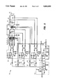
- FIG. 1 is a diagrammatic illustration of state variable feedback-controlled class D audio amplifier circuit in accordance with an embodiment of the invention.
- FIGS. 2 and 3 are schematic circuit diagrams of an implementation of the audio amplifier circuit of FIG. 1.
- FIG. 1 diagrammatically illustrates a state variable feedback-controlled class D audio amplifier circuit in accordance with an embodiment of the invention
- FIGS. 2 and 3 are schematic diagrams showing the details of the respective components of which the amplifier circuit of FIG. 1 is configured.
- the present invention has particular utility in a telephone voice paging amplifier system, where the output (paging speaker) load can be expected to vary from installation to installation.
- a telephone voice paging system where the present invention may be used is described in co-pending application Ser. No. 08/073,200, filed on even date herewith, entitled "Phone Keypad-Sourced Volume Control for Paging System," by R. Soto et al, assigned to the assignee of the present application and the disclosure of which is herein incorporated.
- the inventive state variable feedback-controlled class D audio amplifier circuit is shown as comprising an input port 11 to which an audio signal to be amplified is applied.
- the phrases ⁇ audio signal ⁇ or ⁇ voice paging signal ⁇ are used in the ordinary sense, being understood to encompass audio band frequencies (on the order of 20 Hz-20 KHz).
- Input port 11 is coupled (via a scaling amplifier 12 and input resistor 14, FIG. 2) to a summing node 13 of an error amplifier 15, to which the output of a state variable feedback network 21, to be described, is connected.
- the combined voltage at summing node 13 is amplified by error amplifier 15 and the resultant signal (ERR BAR, FIG.
- Pulse width modulator circuit 23 may employ a DC motor controller chip UC3637N, manufactured by Unitrode Corp., which outputs a periodic pulse waveform on respective output links 24, 26, having a duty cycle proportional to the resultant audio input signal ERR BAR from error amplifier 15.
- gate drive circuit 25 for controlling the (switching) operation of a power H-bridge-configured switching (modulation) circuit 30.
- gate drive circuit 25 comprises first and second pairs of push-pull bipolar transistor drive circuits 31, 32, the base drives for which are coupled to links 24, 26 and outputs of which are transformer coupled, at 33, 34, to respective pairs of FET drive transistor circuits 35, 36, having respective pairs of complementary output drive links 7, 38 and 39, 40.
- the complementary output drive links 37, 38 and 39, 40 of gate drive circuit 25 are coupled to respective drive (gating) inputs of respective pairs of power FET switching transistor circuits 41, 42 and 43, 44 that form respective arms of a power switching circuit 30.
- power switching circuit 30 is operative to both source and sink current with respect to the output audio circuit (transformer-coupled paging speaker).
- the power FET circuits 41, 42, 43, and 44 are operative to controllably switch, to respective pairs of output terminals 45, 46, 46, 48, relatively large magnitude ,opposite polarity voltages (e.g. on the order of ⁇ 75 volts for driving the paging speaker at a prescribed amplification level), provided at complementary power supply terminals 49, 50.
- the switched output of PWM-driven power bridge circuit 30 is a high energy square wave-type signal, which is filtered in a downstream audio filter circuit 51.
- Audio filter circuit 51 is configured as an inductive-capacitive (LC) network, shown in detail in FIG. 2 as comprising respective pairs of inductor windings 52, 53 wound on the same common core and a second pair of inductor windings 54, respective ones of which are wound on a common core and coupled in series with windings 52 and 53.
- LC inductive-capacitive
- Completing the filter are capacitors 55 and 56 which bridge the input and output terminals of inductor winding pair 54.
- Audio filter circuit 51 is operative to filter the square wave output drive signal of bridge circuit 30, so as to preserve the desired audio signal, while filtering out switching transients, and thereby drive the AC paging speaker output load 57 with the only the desired audio paging signal.
- state variable feedback network 21 is coupled to monitor variations in current flow through the inductor components and voltages across capacitor components and input and output terminals of the audio filter circuit 51 and sums the monitored variations to produce an error signal.
- filter input terminals 45, 46, 47, 48 are coupled in respective pairs to respective differential input ports of differential amplifier 61, the output of which is coupled through a summing resistor 63 to summing node 13.
- filter output terminals 58, 59 are coupled to the respective differential input ports of differential amplifier 71, the output of which is coupled through a summing resistor 65 to summing node 13. Also the voltage across capacitor 55 is coupled to the differential input ports of differential amplifier 73, the output of which is coupled through a summing resistor 67 to summing node 13.
- an additional inductor winding 75 is co-wound on the same core with inductors 52, 53 and its output voltage is coupled to an integrator 81.
- the output of integrator 81 is representative of the current through inductors 52, 53, which is applied through summing resistor 83 to summing node 13.
- an additional inductor winding 77 is co-wound on the same core with inductor 54 and its output voltage is coupled to an integrator 85.
- the output of integrator 85 is representative of the current through inductor 54, which is applied through summing resistor 87 to summing node 13.
- the resultant signal at summing node 13 is a combination of state variables of the audio filter plus the audio input signal supplied to audio input port 11.
- This resultant audio drive signal is output by error amplifier 15 for driving pulse width modulator 23.
- the characteristics of the LC audio filter 51 will vary with the load (one or more speakers 57 of the voice paging system) to which output of the audio filter 51 is coupled.
- the state variable feedback network 21 allows the class D audio paging amplifier circuit of FIGS. 1-3 to attain stability and provide the necessary drive characteristic to the audio filter, so that the frequency response of the filter remains generally flat.
Abstract
Description
Claims (24)
Priority Applications (4)
| Application Number | Priority Date | Filing Date | Title |
|---|---|---|---|
| US08/073,204 US5410592A (en) | 1993-06-04 | 1993-06-04 | Class `D` audio speaker amplifier circuit with state variable feedback control |
| CA002124976A CA2124976A1 (en) | 1993-06-04 | 1994-06-02 | Class 'd' audio speaker amplifier circuit with state variable feedback control |
| CN94106511A CN1105788A (en) | 1993-06-04 | 1994-06-04 | Class 'D' audio speaker amplifier circuit with state variable feedback control |
| KR1019940012653A KR950002321A (en) | 1993-06-04 | 1994-06-04 | Class D audio speaker amplifier circuit with state variable feedback controller |
Applications Claiming Priority (1)
| Application Number | Priority Date | Filing Date | Title |
|---|---|---|---|
| US08/073,204 US5410592A (en) | 1993-06-04 | 1993-06-04 | Class `D` audio speaker amplifier circuit with state variable feedback control |
Publications (1)
| Publication Number | Publication Date |
|---|---|
| US5410592A true US5410592A (en) | 1995-04-25 |
Family
ID=22112368
Family Applications (1)
| Application Number | Title | Priority Date | Filing Date |
|---|---|---|---|
| US08/073,204 Expired - Fee Related US5410592A (en) | 1993-06-04 | 1993-06-04 | Class `D` audio speaker amplifier circuit with state variable feedback control |
Country Status (4)
| Country | Link |
|---|---|
| US (1) | US5410592A (en) |
| KR (1) | KR950002321A (en) |
| CN (1) | CN1105788A (en) |
| CA (1) | CA2124976A1 (en) |
Cited By (38)
| Publication number | Priority date | Publication date | Assignee | Title |
|---|---|---|---|---|
| WO1997020426A1 (en) * | 1995-11-29 | 1997-06-05 | Philips Electronics N.V. | Terminal for wirebound telecommunication |
| US5696468A (en) * | 1996-02-29 | 1997-12-09 | Qualcomm Incorporated | Method and apparatus for autocalibrating the center frequency of a voltage controlled oscillator of a phase locked loop |
| EP0833443A1 (en) * | 1996-09-27 | 1998-04-01 | Harris Corporation | Switching amplifier closed loop dual comparator modulation technique |
| US5805020A (en) * | 1996-06-27 | 1998-09-08 | Harris Corporation | Silent start class D amplifier |
| US5815581A (en) * | 1995-10-19 | 1998-09-29 | Mitel Semiconductor, Inc. | Class D hearing aid amplifier with feedback |
| US5838807A (en) * | 1995-10-19 | 1998-11-17 | Mitel Semiconductor, Inc. | Trimmable variable compression amplifier for hearing aid |
| US5898340A (en) * | 1996-11-20 | 1999-04-27 | Chatterjee; Manjirnath A. | High power efficiency audio amplifier with digital audio and volume inputs |
| US5949282A (en) * | 1998-02-25 | 1999-09-07 | National Semiconductor Corporation | Class D amplifier no low pass filter feedback with zero phase delay |
| WO1999045641A1 (en) * | 1998-03-03 | 1999-09-10 | Toccata Technology Aps | A method in the compensation of unlinearities in an amplifier, an amplifier, and uses of the method and the amplifier |
| US6016075A (en) * | 1997-06-04 | 2000-01-18 | Lord Corporation | Class-D amplifier input structure |
| US6107875A (en) * | 1998-10-15 | 2000-08-22 | Intersil Corporation | Variable frequency class D modulator with built in soft clipping and frequency limiting |
| US6127885A (en) * | 1998-08-31 | 2000-10-03 | Cello, Limited | Class D amplifiers including transition zone modulation |
| US6140875A (en) * | 1997-08-12 | 2000-10-31 | U.S. Philips Corporation | Device for amplifying digital signals |
| US6249182B1 (en) * | 1998-11-18 | 2001-06-19 | Intersil Corporation | Class D amplifier with bandwidth independent of load impedance |
| US6396933B1 (en) * | 1997-02-24 | 2002-05-28 | Korea Advanced Institute Of Science And Technology | High-fidelity and high-efficiency analog amplifier combined with digital amplifier |
| US6441685B1 (en) | 2000-03-17 | 2002-08-27 | Jl Audio, Inc. | Amplifier circuit and method for providing negative feedback thereto |
| US6542031B2 (en) * | 2001-09-05 | 2003-04-01 | Pericom Semiconductor Corp. | Switched IOH and IOL current sources for CMOS low-voltage PECL driver with self-timed pull-down current boost |
| US6545533B2 (en) | 2000-12-18 | 2003-04-08 | Texas Instruments Incorporated | Class D audio speaker amplifier circuit with pseudo noise modulation |
| US6650232B1 (en) * | 1996-09-11 | 2003-11-18 | Robert Bosch Gmbh | Sounder control system |
| EP0935846B1 (en) * | 1996-10-31 | 2003-12-03 | Bang & Olufsen A/S | Pulse modulation power amplifier with enhanced cascade control method |
| US6687380B1 (en) | 1999-12-17 | 2004-02-03 | Broan-Nutone Llc | Active sub-woofer speaker system |
| US6753729B2 (en) * | 2000-01-06 | 2004-06-22 | Mitek Corporation | Self-oscillating variable frequency closed loop Class D amplifier |
| EP1455445A1 (en) * | 2002-08-22 | 2004-09-08 | Matsushita Electric Industrial Co., Ltd. | Digital amplification device |
| EP1630954A1 (en) * | 2004-08-24 | 2006-03-01 | Flying Mole Corporation | A feedback circuit |
| US20060072776A1 (en) * | 1999-12-17 | 2006-04-06 | Tejaswi Vishwamitra | Amplifier and sub-woofer speaker system |
| US20060114057A1 (en) * | 2004-12-01 | 2006-06-01 | Creative Technology Ltd. | Power multiplier system and method |
| US20060290549A1 (en) * | 2005-06-27 | 2006-12-28 | Rajiv Laroia | Methods and apparatus for implementing and/or using amplifiers and/or for performing various amplification related operations |
| WO2007099442A1 (en) * | 2006-03-03 | 2007-09-07 | Bang & Olufsen Icepower A/S | Hybrid feedback controlled oscillation modulator and switching power amplifier system |
| US7289050B1 (en) | 2005-06-27 | 2007-10-30 | Qualcomm Incorporated | Amplification method and apparatus |
| US20080111619A1 (en) * | 2006-11-15 | 2008-05-15 | Analog Devices, Inc. | Apparatus and method for controlling a common-mode voltage of switching amplifiers |
| US7702120B1 (en) | 2005-01-31 | 2010-04-20 | Bogen Communications, Inc. | Self-amplified loudspeakers with switching amplifier technology |
| WO2011129553A3 (en) * | 2010-04-13 | 2012-03-15 | 주식회사 아빈크 | Public address amplifier which is lightweight due to the supply of class-d sampling frequency to opt |
| US8553909B2 (en) | 2011-04-29 | 2013-10-08 | Smsc Holdings S.A.R.L. | Low-power class D amplifier using multistate analog feedback loops |
| CN104333835A (en) * | 2013-07-22 | 2015-02-04 | 上声电子(苏州工业园区)有限公司 | D type power amplifying loudspeaker |
| US8963634B2 (en) | 2012-02-28 | 2015-02-24 | Qualcomm Incorporated | Load current sensing |
| US20150124983A1 (en) * | 2013-11-01 | 2015-05-07 | Realtek Semiconductor Corp. | Circuit and method for driving a loudspeaker |
| US20150229284A1 (en) * | 2010-06-25 | 2015-08-13 | Panasonic Intellectual Property Management Co., Ltd. | Amplifier apparatus |
| CN112865730A (en) * | 2019-11-27 | 2021-05-28 | 瑞昱半导体股份有限公司 | Class D amplifier circuit and audio amplification method |
Families Citing this family (9)
| Publication number | Priority date | Publication date | Assignee | Title |
|---|---|---|---|---|
| TW437161B (en) * | 1995-08-30 | 2001-05-28 | Sony Corp | Audio signal amplifying apparatus |
| US6535399B2 (en) * | 2001-08-14 | 2003-03-18 | Bose Corporation | Tracking power supply controlling |
| JP3776392B2 (en) * | 2002-10-03 | 2006-05-17 | 三菱電機株式会社 | Class D amplifier |
| EP1614215A1 (en) * | 2003-04-07 | 2006-01-11 | Philips Intellectual Property & Standards GmbH | Digital amplifier |
| KR101128520B1 (en) * | 2005-10-24 | 2012-03-27 | 삼성전자주식회사 | digital audio amplifier and a method of amplifying digital audio |
| KR100796319B1 (en) * | 2006-10-02 | 2008-01-21 | 엘리트 세미컨덕터 메모리 테크놀로지 인코퍼레이티드 | Class-d audio amplifier with half-swing pulse-width-modulation |
| US7843260B2 (en) * | 2008-10-31 | 2010-11-30 | Monolithic Power Systems, Inc. | Method and apparatus for high performance class D audio amplifiers |
| US11063565B2 (en) * | 2018-02-23 | 2021-07-13 | Qsc, Llc | Audio amplifier assemblies, processes, and methods |
| CN110446146A (en) * | 2019-08-07 | 2019-11-12 | 常州科先达通讯技术有限公司 | Smart speakers |
Citations (6)
| Publication number | Priority date | Publication date | Assignee | Title |
|---|---|---|---|---|
| US4178556A (en) * | 1977-04-22 | 1979-12-11 | Attwood Brian E | Class D amplifier system |
| US4720848A (en) * | 1983-12-05 | 1988-01-19 | Nippo Communication Industrial Co. | Communication system with voice announcement means |
| US4885577A (en) * | 1988-03-02 | 1989-12-05 | Motorola, Inc. | Paging system for providing a data message and a voice message to a unique address of a paging receiver |
| US5063332A (en) * | 1990-12-21 | 1991-11-05 | General Electric Company | Feedback control system for a high-efficiency class-D power amplifier circuit |
| US5160896A (en) * | 1992-02-18 | 1992-11-03 | Harman International Industries, Incorporated | Class D amplifier |
| US5200711A (en) * | 1990-10-26 | 1993-04-06 | AB Lab. Gruppen Andersson & Bavholm | Pulse-width modulated, linear audio-power amplifier |
-
1993
- 1993-06-04 US US08/073,204 patent/US5410592A/en not_active Expired - Fee Related
-
1994
- 1994-06-02 CA CA002124976A patent/CA2124976A1/en not_active Abandoned
- 1994-06-04 KR KR1019940012653A patent/KR950002321A/en not_active Application Discontinuation
- 1994-06-04 CN CN94106511A patent/CN1105788A/en active Pending
Patent Citations (6)
| Publication number | Priority date | Publication date | Assignee | Title |
|---|---|---|---|---|
| US4178556A (en) * | 1977-04-22 | 1979-12-11 | Attwood Brian E | Class D amplifier system |
| US4720848A (en) * | 1983-12-05 | 1988-01-19 | Nippo Communication Industrial Co. | Communication system with voice announcement means |
| US4885577A (en) * | 1988-03-02 | 1989-12-05 | Motorola, Inc. | Paging system for providing a data message and a voice message to a unique address of a paging receiver |
| US5200711A (en) * | 1990-10-26 | 1993-04-06 | AB Lab. Gruppen Andersson & Bavholm | Pulse-width modulated, linear audio-power amplifier |
| US5063332A (en) * | 1990-12-21 | 1991-11-05 | General Electric Company | Feedback control system for a high-efficiency class-D power amplifier circuit |
| US5160896A (en) * | 1992-02-18 | 1992-11-03 | Harman International Industries, Incorporated | Class D amplifier |
Cited By (60)
| Publication number | Priority date | Publication date | Assignee | Title |
|---|---|---|---|---|
| US5815581A (en) * | 1995-10-19 | 1998-09-29 | Mitel Semiconductor, Inc. | Class D hearing aid amplifier with feedback |
| US5838807A (en) * | 1995-10-19 | 1998-11-17 | Mitel Semiconductor, Inc. | Trimmable variable compression amplifier for hearing aid |
| US5848147A (en) * | 1995-11-29 | 1998-12-08 | U.S. Philips Corporation | Terminal for wirebound telecommunication |
| WO1997020426A1 (en) * | 1995-11-29 | 1997-06-05 | Philips Electronics N.V. | Terminal for wirebound telecommunication |
| US5696468A (en) * | 1996-02-29 | 1997-12-09 | Qualcomm Incorporated | Method and apparatus for autocalibrating the center frequency of a voltage controlled oscillator of a phase locked loop |
| US5805020A (en) * | 1996-06-27 | 1998-09-08 | Harris Corporation | Silent start class D amplifier |
| US6650232B1 (en) * | 1996-09-11 | 2003-11-18 | Robert Bosch Gmbh | Sounder control system |
| EP0833443A1 (en) * | 1996-09-27 | 1998-04-01 | Harris Corporation | Switching amplifier closed loop dual comparator modulation technique |
| US5767740A (en) * | 1996-09-27 | 1998-06-16 | Harris Corporation | Switching amplifier closed loop dual comparator modulation technique |
| EP0935846B1 (en) * | 1996-10-31 | 2003-12-03 | Bang & Olufsen A/S | Pulse modulation power amplifier with enhanced cascade control method |
| US5898340A (en) * | 1996-11-20 | 1999-04-27 | Chatterjee; Manjirnath A. | High power efficiency audio amplifier with digital audio and volume inputs |
| US6396933B1 (en) * | 1997-02-24 | 2002-05-28 | Korea Advanced Institute Of Science And Technology | High-fidelity and high-efficiency analog amplifier combined with digital amplifier |
| US6016075A (en) * | 1997-06-04 | 2000-01-18 | Lord Corporation | Class-D amplifier input structure |
| US6140875A (en) * | 1997-08-12 | 2000-10-31 | U.S. Philips Corporation | Device for amplifying digital signals |
| US5949282A (en) * | 1998-02-25 | 1999-09-07 | National Semiconductor Corporation | Class D amplifier no low pass filter feedback with zero phase delay |
| WO1999045641A1 (en) * | 1998-03-03 | 1999-09-10 | Toccata Technology Aps | A method in the compensation of unlinearities in an amplifier, an amplifier, and uses of the method and the amplifier |
| US8098091B1 (en) | 1998-03-03 | 2012-01-17 | Texas Instruments Denmark | Method in the compensation of unlinearities in an amplifier, and uses of the method and the amplifier |
| US6127885A (en) * | 1998-08-31 | 2000-10-03 | Cello, Limited | Class D amplifiers including transition zone modulation |
| US6107875A (en) * | 1998-10-15 | 2000-08-22 | Intersil Corporation | Variable frequency class D modulator with built in soft clipping and frequency limiting |
| US6249182B1 (en) * | 1998-11-18 | 2001-06-19 | Intersil Corporation | Class D amplifier with bandwidth independent of load impedance |
| US20060072776A1 (en) * | 1999-12-17 | 2006-04-06 | Tejaswi Vishwamitra | Amplifier and sub-woofer speaker system |
| US6687380B1 (en) | 1999-12-17 | 2004-02-03 | Broan-Nutone Llc | Active sub-woofer speaker system |
| US6753729B2 (en) * | 2000-01-06 | 2004-06-22 | Mitek Corporation | Self-oscillating variable frequency closed loop Class D amplifier |
| US6441685B1 (en) | 2000-03-17 | 2002-08-27 | Jl Audio, Inc. | Amplifier circuit and method for providing negative feedback thereto |
| US6545533B2 (en) | 2000-12-18 | 2003-04-08 | Texas Instruments Incorporated | Class D audio speaker amplifier circuit with pseudo noise modulation |
| US6542031B2 (en) * | 2001-09-05 | 2003-04-01 | Pericom Semiconductor Corp. | Switched IOH and IOL current sources for CMOS low-voltage PECL driver with self-timed pull-down current boost |
| EP1455445A1 (en) * | 2002-08-22 | 2004-09-08 | Matsushita Electric Industrial Co., Ltd. | Digital amplification device |
| EP1455445A4 (en) * | 2002-08-22 | 2005-03-23 | Matsushita Electric Ind Co Ltd | Digital amplification device |
| US20050113055A1 (en) * | 2002-08-22 | 2005-05-26 | Matsushita Electric Industrial Co Ltd. | Digital amplification device |
| US7202742B2 (en) * | 2002-08-22 | 2007-04-10 | Matsushita Electric Industrial Co., Ltd. | Digital amplification device |
| JP2006066998A (en) * | 2004-08-24 | 2006-03-09 | Flying Mole Corp | Feedback circuit |
| US20060044059A1 (en) * | 2004-08-24 | 2006-03-02 | Flying Mole Corporation | Feedback circuit |
| EP1630954A1 (en) * | 2004-08-24 | 2006-03-01 | Flying Mole Corporation | A feedback circuit |
| US7279970B2 (en) | 2004-08-24 | 2007-10-09 | Flying Mole Corporation | Feedback circuit |
| WO2006059956A1 (en) * | 2004-12-01 | 2006-06-08 | Creative Technology Ltd | A power multiplier apparatus and method |
| US7116168B2 (en) | 2004-12-01 | 2006-10-03 | Creative Technology Ltd | Power multiplier system and method |
| US20060114057A1 (en) * | 2004-12-01 | 2006-06-01 | Creative Technology Ltd. | Power multiplier system and method |
| US7702120B1 (en) | 2005-01-31 | 2010-04-20 | Bogen Communications, Inc. | Self-amplified loudspeakers with switching amplifier technology |
| WO2007002770A3 (en) * | 2005-06-27 | 2007-03-22 | Qualcomm Flarion Tech | Methods and apparatus for implementing and using amplifiers for performing various amplification related operations |
| US7289050B1 (en) | 2005-06-27 | 2007-10-30 | Qualcomm Incorporated | Amplification method and apparatus |
| US7405686B2 (en) | 2005-06-27 | 2008-07-29 | Qualcomm Incorporated | Methods and apparatus for implementing and/or using amplifiers and/or for performing various amplification related operations |
| WO2007002770A2 (en) * | 2005-06-27 | 2007-01-04 | Qualcomm Flarion Technologies, Inc. | Methods and apparatus for implementing and using amplifiers for performing various amplification related operations |
| US20060290549A1 (en) * | 2005-06-27 | 2006-12-28 | Rajiv Laroia | Methods and apparatus for implementing and/or using amplifiers and/or for performing various amplification related operations |
| CN101273530B (en) * | 2005-06-27 | 2011-02-09 | 高通股份有限公司 | Methods and apparatus for implementing and/or using amplifiers and/or for performing various amplification related operations |
| WO2007099442A1 (en) * | 2006-03-03 | 2007-09-07 | Bang & Olufsen Icepower A/S | Hybrid feedback controlled oscillation modulator and switching power amplifier system |
| CN101395793B (en) * | 2006-03-03 | 2012-08-29 | B&Oice动力公司 | Hybrid feedback controlled oscillation modulator and switching power amplifier system |
| US8013678B2 (en) | 2006-03-03 | 2011-09-06 | Bang & Olufsen Icepower A/S, Gi. | Hybrid feedback controlled oscillation modulator and switching power amplifier system |
| US20100253396A1 (en) * | 2006-11-15 | 2010-10-07 | Analog Devices, Inc. | Apparatus and method for controlling a common-mode voltage of switching amplifiers |
| US7772924B2 (en) * | 2006-11-15 | 2010-08-10 | Analog Devices, Inc. | Apparatus and method for controlling a common-mode voltage of switching amplifiers |
| US20080111619A1 (en) * | 2006-11-15 | 2008-05-15 | Analog Devices, Inc. | Apparatus and method for controlling a common-mode voltage of switching amplifiers |
| US8416016B2 (en) | 2006-11-15 | 2013-04-09 | Analog Devices, Inc. | Apparatus and method for controlling a common-mode voltage of switching amplifiers |
| WO2011129553A3 (en) * | 2010-04-13 | 2012-03-15 | 주식회사 아빈크 | Public address amplifier which is lightweight due to the supply of class-d sampling frequency to opt |
| US20150229284A1 (en) * | 2010-06-25 | 2015-08-13 | Panasonic Intellectual Property Management Co., Ltd. | Amplifier apparatus |
| US9257945B2 (en) * | 2010-06-25 | 2016-02-09 | Panasonic Intellectual Property Management Co., Ltd. | Amplifier apparatus |
| US8553909B2 (en) | 2011-04-29 | 2013-10-08 | Smsc Holdings S.A.R.L. | Low-power class D amplifier using multistate analog feedback loops |
| US8963634B2 (en) | 2012-02-28 | 2015-02-24 | Qualcomm Incorporated | Load current sensing |
| CN104333835A (en) * | 2013-07-22 | 2015-02-04 | 上声电子(苏州工业园区)有限公司 | D type power amplifying loudspeaker |
| US20150124983A1 (en) * | 2013-11-01 | 2015-05-07 | Realtek Semiconductor Corp. | Circuit and method for driving a loudspeaker |
| US9826312B2 (en) * | 2013-11-01 | 2017-11-21 | Realtek Semiconductor Corp. | Circuit and method for driving a loudspeaker |
| CN112865730A (en) * | 2019-11-27 | 2021-05-28 | 瑞昱半导体股份有限公司 | Class D amplifier circuit and audio amplification method |
Also Published As
| Publication number | Publication date |
|---|---|
| CA2124976A1 (en) | 1994-12-05 |
| KR950002321A (en) | 1995-01-04 |
| CN1105788A (en) | 1995-07-26 |
Similar Documents
| Publication | Publication Date | Title |
|---|---|---|
| US5410592A (en) | Class `D` audio speaker amplifier circuit with state variable feedback control | |
| US7907010B2 (en) | Digital amplifier | |
| US6016075A (en) | Class-D amplifier input structure | |
| US6211728B1 (en) | Modulation scheme for filterless switching amplifiers | |
| US5442317A (en) | Switching regulator and amplifier system | |
| EP0483094B1 (en) | A pulse-width modulated, linear audio-power amplifier | |
| US20030198063A1 (en) | Audio band conducted emissions suppression on power feeders | |
| US9793867B2 (en) | Method and apparatus for achieving very high-output signal swing from class-D amplifier using fewer components | |
| KR19990044094A (en) | Opposed Current Power Converter | |
| US9973157B2 (en) | Method and apparatus for achieving high-output signal swing from class-D amplifier | |
| EP1825592B1 (en) | A power multiplier apparatus and method | |
| US4521726A (en) | Control circuitry for a pulse-width-modulated switching power supply | |
| WO2020146591A1 (en) | Class d amplifier current feedback | |
| WO2019030518A1 (en) | An error amplifier | |
| US6188276B1 (en) | Power amplifier | |
| US20050078848A1 (en) | Power amplifier and method for split voice coil transducer or speaker | |
| EP1234377B1 (en) | Power booster amplifier | |
| US6753729B2 (en) | Self-oscillating variable frequency closed loop Class D amplifier | |
| US6882219B2 (en) | High frequency switch-mode power amplifier | |
| US20030095000A1 (en) | Apparatus with ultra high output power class D audio amplifier | |
| EP1269623B1 (en) | High frequency switch-mode power amplifier | |
| US20070104338A1 (en) | Amplifier Arrangement and Distributed Audio System | |
| JP2006522528A (en) | Digital amplifier | |
| US5682302A (en) | Adaptable power converter applying digitized-wave-generation for integrated circuit implementation | |
| Joshi et al. | Design of an analog sliding mode controlled audio amplifier |
Legal Events
| Date | Code | Title | Description |
|---|---|---|---|
| AS | Assignment |
Owner name: HARRIS CORPORATION, FLORIDA Free format text: ASSIGNMENT OF ASSIGNORS INTEREST;ASSIGNORS:WAGNER, RANDALL M.;MISTRY, YOGI L.;REEL/FRAME:006680/0706 Effective date: 19930830 |
|
| FEPP | Fee payment procedure |
Free format text: PAYOR NUMBER ASSIGNED (ORIGINAL EVENT CODE: ASPN); ENTITY STATUS OF PATENT OWNER: LARGE ENTITY |
|
| FPAY | Fee payment |
Year of fee payment: 4 |
|
| AS | Assignment |
Owner name: VALCOM, INC. (A VIRGINIA CORPORATION), VIRGINIA Free format text: ASSIGNMENT OF ASSIGNORS INTEREST;ASSIGNOR:HARRIS CORPORATION (A DELAWARE CORPORATION);REEL/FRAME:010272/0870 Effective date: 19990707 |
|
| REMI | Maintenance fee reminder mailed | ||
| LAPS | Lapse for failure to pay maintenance fees | ||
| STCH | Information on status: patent discontinuation |
Free format text: PATENT EXPIRED DUE TO NONPAYMENT OF MAINTENANCE FEES UNDER 37 CFR 1.362 |
|
| FP | Lapsed due to failure to pay maintenance fee |
Effective date: 20030425 |