US5426646A - Instantaneous bit-error-rate meter - Google Patents
Instantaneous bit-error-rate meter Download PDFInfo
- Publication number
- US5426646A US5426646A US07/904,111 US90411192A US5426646A US 5426646 A US5426646 A US 5426646A US 90411192 A US90411192 A US 90411192A US 5426646 A US5426646 A US 5426646A
- Authority
- US
- United States
- Prior art keywords
- error
- pulses
- rate
- bit
- timing
- Prior art date
- Legal status (The legal status is an assumption and is not a legal conclusion. Google has not performed a legal analysis and makes no representation as to the accuracy of the status listed.)
- Expired - Fee Related
Links
Images
Classifications
-
- G—PHYSICS
- G06—COMPUTING; CALCULATING OR COUNTING
- G06F—ELECTRIC DIGITAL DATA PROCESSING
- G06F11/00—Error detection; Error correction; Monitoring
- G06F11/07—Responding to the occurrence of a fault, e.g. fault tolerance
- G06F11/0703—Error or fault processing not based on redundancy, i.e. by taking additional measures to deal with the error or fault not making use of redundancy in operation, in hardware, or in data representation
- G06F11/0751—Error or fault detection not based on redundancy
- G06F11/0754—Error or fault detection not based on redundancy by exceeding limits
- G06F11/076—Error or fault detection not based on redundancy by exceeding limits by exceeding a count or rate limit, e.g. word- or bit count limit
-
- H—ELECTRICITY
- H04—ELECTRIC COMMUNICATION TECHNIQUE
- H04L—TRANSMISSION OF DIGITAL INFORMATION, e.g. TELEGRAPHIC COMMUNICATION
- H04L1/00—Arrangements for detecting or preventing errors in the information received
- H04L1/20—Arrangements for detecting or preventing errors in the information received using signal quality detector
Definitions
- This invention pertains broadly to the field of digital communications. More particularly, the invention relates to an apparatus that discloses the error percentage or rate that a received digital data stream differs from its transmitted digital data stream.
- bit-error-rate (BER) measuring instruments or methods have been based on taking a large sample of a digital transmission over an extended period of time. During this time, transmitted bits were compared with received bits. Error pulses were counted for each received bit lacking correspondence with its transmitted bit. The number of errors was then divided by the total number of bits transmitted to give a BER measurement (i.e. the percentage of bits in error). This process took several minutes to tens of minutes or even longer just to obtain a single BER reading. Besides taking a long time, the measurements obtained were only the averaged values over the measurement period. Because of this averaging, moment-to-moment variations of BER or what is known in the art as the "burstiness" of the errors were not indicated.
- the instantaneous bit-error-rate meter (IBERM) of the invention is designed to provide an instantaneous, real-time reading of bit-error-rate for digital communications systems.
- Bit error pulses derived through an apparatus and/or a method independent of the invention to be described herein, are input into the instantaneous bit error rate meter.
- the error pulses are first filtered in a buffer stage to provide input impedance matching and desensitization to pulse variations in amplitude, rise-time and pulse width.
- the bit-error pulses are thereby transformed into signals of predictable characteristics. These transformed error pulses are then used as trigger signals to be applied to a timing pulse generator.
- the timing pulse generator generates a timing pulse for each transformed bit-error pulse, and is calibrated to generate timing pulses having a preselected width that corresponds to the baud rate of the communications system being monitored.
- An integrator is then used to generate voltage from the timing pulses when they are present.
- the voltage corresponds to the bit-error-rate of the communications system being observed and is sent to a meter driver section that conditions the voltage for meter display.
- Another object of the invention is to provide an improved bit-error-rate meter that permits real-time reading of bit-error-rate.
- Yet a further object of the invention is to provide an improved bit-error-rate meter that permits instantaneous bit-error-rate readings that are limited in time only by circuit propagation and meter response delays.
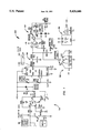
- FIG. 1 is a schematic of a representative implementation of the invention.
- an instantaneous bit-error-rate meter (IBERM) 100 is shown.
- Input to the IBERM are error pulses 110 indicative of the discrepancy between a transmitted digital data stream and this stream as received by a communication system being monitored.
- Error pulses such as these are derived through the invention described in U.S. Pat. No. 3,824,548 incorporated by reference herein, and in particular the output of element 50, the bit comparison circuit of this invention. These error pulses indicate that received bits are not identical to transmitted bits.
- Switch S1 of the invention provides the user with a choice of input impedances.
- a 10 k ohm impedance is made available for typical transistor-transistor logic (TTL) inputs whereas a 50 ohm resistor R1 is provided for cases where error pulses are received over a typical 50 ohm coaxial line.
- TTL transistor-transistor logic
- Operational high gain amplifier U1 such as an LS357, is part of a buffer stage 120 that provides input impedance matching and desensitization to variations in error pulse amplitude, rise-time and pulse width.
- Resistors R3 and R4 provide a threshold input level of about one volt in this implementation to suppress input noise and offset voltages.
- Resistors R2 and R5 gives U1 a gain of about ten. With no input, the one-volt offset at pin 3 of amplifier U1 is amplified to give a +10 volts output at pin 6. When the input to amplifier U1 exceeds 2.5 volts, the amplifier saturates, amplifying the 1.5 volt differential input to the -15 VDC power supply level.
- the output of amplifier U1 is differentiated to provide a trigger signal of narrow signal characteristics. This output is differentiated by capacitor C1 and resistor R6, and the positive going transition is clipped to +15 volts by diode D1 that serves as a circuit protector.
- diode D1 that serves as a circuit protector.
- This outputted timing pulse is determined by the time constant of the R7, RS, C2 network and is set to correspond to the baud rate of the digital communications system being monitored as will be further explained.
- C2 will be discharged.
- a trigger pulse at pin 2 of U2 opens up the discharge path, allowing C2 to charge towards +15 volts at a rate determined by R7 and R8.
- C2 charges to +10 volts at pin 6 and 7 of U2, U2 resets, ending the output timing pulse at pin 3.
- Capacitor C3 is for noise filtering.
- the timing pulses outputted from U2 are sent to an integrator 130 including R9, R10 and C4.
- the resulting DC voltage of the integrated output pulses is attenuated by R11 to provide a reasonably small input impedance to amplifier U3.
- U3 serves as part of a meter drive circuit 140 as will be further explained.
- Capacitors C5 through C9 provide optional damping of the U3 input voltage as may be selected by switch S3.
- Resistors R12, R13 and R14 set the gain of operational amplifier U3.
- Amplifier U3 (which may be, for example, an OP77) provides the gain and drive capability to control meter M1.
- Switch S2 selects the meter scale so that a user may read either a 10% or 100% bit-error-rate at the full scale of the meter.
- R15 produces a full-scale reading on the meter, providing 1 ma of current for a 10 VDC output from U3, pin 6.
- R16 and R17 provide a 1 ma current to produce a full-scale reading on M1 with an output from U3 of 1 VDC.
- Diodes D2 and D3 provide meter protection on the 10% scale by limiting the voltage at the R16 input to about 1.5 VDC, thereby limiting meter current to about 1.5 ma maximum.
- a ⁇ 15 VDC power supply (P.S.) 150, along with fuse F1 and power switch S4, provide power to IBERM 100.
- Operation of the invention is as follows: for a digital communications system operating at 50 baud, for example, the invention is calibrated by injecting simulated error pulses at 50 pulses per second (PPS).
- the 50 PPS represent a 100% BER at 50 baud.
- the invention is adjusted at this time to read a 100% BER on meter M1. This adjustment is done by setting the Baud Rate pot, RS, for its maximum resistance (25K) and adjusting resistor R13 for a full-scale meter reading with switch S2 in the 100% position. Under these conditions, timing pulse generator U2 generates timing pulses about 15 msec long every 20 msec. These pulses are then integrated by integration network 130 including the combination of R9, R10, and C4.
- timing pulse generator U2 will produce proportionately fewer pulses per second and a correspondingly lower voltage will be produced by the integration network of R9, R10 and C4, thereby giving a lower BER measurement on meter M1.
- error pulses will occur more often for a given bit-error-rate.
- the Baud Rate pot R8 is set so that the output timing pulse width of U2 is correspondingly less, so that the bit-error-rate meter M1 reads properly.
- R8 would be set to a preselected 100 baud position which will give a U2 timing pulse width of 7.5 msec, one-half of that for the 50 baud rate.
- the timing pulse output of U2 will then be 7.5 msec pulses every 10 msec (for a 100% BER) instead of the 15 msec every 20 msec for the 50 baud case.
- the same duty cycle i.e. 0.75) is thus produced, giving an equal charging time to integrator components 130, and producing an equal 100% reading on meter M1.
- IBERM circuit 100 is designed to operate with baud rates from 50 to 1200 baud.
- potentiometer R7 is used and Baud Rate pot R8 is set to minimum resistance.
- the invention is designed to read BER levels from 1 to 100% and provides bit-error-rate scales of 10 and 100%. For low error rates at low baud rates (e.g. 1% BER at 50 baud), errors will occur very seldom (e.g. once every 2 seconds). Under these conditions, the damping capacitors 160 are required to produce accurate, constant readings.
- circuit values described herein can be changed to operate at much higher baud rates and to measure much lower BER values.
- the design described is essentially all analog, one skilled in the art will realize that increased precision should be realized if more complex digital circuitry were used. Such circuitry would also permit a design such that the sampling time of bit-error-rate measurements could be precisely varied. These design changes could, of course, permit operation of the invention over a wide range of bit rates and at much lower bit-error-rate levels.
Abstract
An instantaneous bit-error-rate meter provides an instantaneous, real-timeeading of bit-error-rate for digital communications data. Bit-error pulses are input into the meter and are first filtered in a buffer stage to provide input impedance matching and desensitization to pulse variations in amplitude, rise-time and pulse-width. The bit-error pulses are transformed into trigger signals for a timing pulse generator. The timing pulse generator generates timing pulses for each transformed bit-error pulse, and is calibrated to generate timing pulses having a preselected pulse width corresponding to the baud rate of the communications data. An integrator generates a voltage from the timing pulses that is representative of the bit-error-rate as a function of the data transmission rate. The integrated voltage is then displayed on a meter to indicate the bit-error-rate.
Description
The invention described herein may be manufactured and used by or for the Government of the United States of America for governmental purposes without the payment of any royalties thereon or therefor.
U.S. Pat. No. 3,824,548 titled "Satellite Communications Link Monitor" issued to Dean R. Sullivan and James E. Pohl is hereby incorporated by reference with all its appertaining documents and references.
2. Field of the Invention
This invention pertains broadly to the field of digital communications. More particularly, the invention relates to an apparatus that discloses the error percentage or rate that a received digital data stream differs from its transmitted digital data stream.
2. Description of the Related Art
In the past, bit-error-rate (BER) measuring instruments or methods have been based on taking a large sample of a digital transmission over an extended period of time. During this time, transmitted bits were compared with received bits. Error pulses were counted for each received bit lacking correspondence with its transmitted bit. The number of errors was then divided by the total number of bits transmitted to give a BER measurement (i.e. the percentage of bits in error). This process took several minutes to tens of minutes or even longer just to obtain a single BER reading. Besides taking a long time, the measurements obtained were only the averaged values over the measurement period. Because of this averaging, moment-to-moment variations of BER or what is known in the art as the "burstiness" of the errors were not indicated.
There is a need in the digital communication field for a device that displays real-time BER instantaneously permitting one to observe how BER is changing with time.
The instantaneous bit-error-rate meter (IBERM) of the invention is designed to provide an instantaneous, real-time reading of bit-error-rate for digital communications systems. Bit error pulses, derived through an apparatus and/or a method independent of the invention to be described herein, are input into the instantaneous bit error rate meter. The error pulses are first filtered in a buffer stage to provide input impedance matching and desensitization to pulse variations in amplitude, rise-time and pulse width. The bit-error pulses are thereby transformed into signals of predictable characteristics. These transformed error pulses are then used as trigger signals to be applied to a timing pulse generator.
The timing pulse generator generates a timing pulse for each transformed bit-error pulse, and is calibrated to generate timing pulses having a preselected width that corresponds to the baud rate of the communications system being monitored.
An integrator is then used to generate voltage from the timing pulses when they are present. The voltage corresponds to the bit-error-rate of the communications system being observed and is sent to a meter driver section that conditions the voltage for meter display.
It is an object of the invention to provide an improved way of indicating bit-error-rate for digital communications systems.
Another object of the invention is to provide an improved bit-error-rate meter that permits real-time reading of bit-error-rate.
Yet a further object of the invention is to provide an improved bit-error-rate meter that permits instantaneous bit-error-rate readings that are limited in time only by circuit propagation and meter response delays.
FIG. 1 is a schematic of a representative implementation of the invention.
Referring to FIG. 1, an instantaneous bit-error-rate meter (IBERM) 100 is shown. Input to the IBERM are error pulses 110 indicative of the discrepancy between a transmitted digital data stream and this stream as received by a communication system being monitored. Error pulses such as these are derived through the invention described in U.S. Pat. No. 3,824,548 incorporated by reference herein, and in particular the output of element 50, the bit comparison circuit of this invention. These error pulses indicate that received bits are not identical to transmitted bits.
Switch S1 of the invention provides the user with a choice of input impedances. In the representative embodiment of the invention shown, a 10 k ohm impedance is made available for typical transistor-transistor logic (TTL) inputs whereas a 50 ohm resistor R1 is provided for cases where error pulses are received over a typical 50 ohm coaxial line.
Operational high gain amplifier U1, such as an LS357, is part of a buffer stage 120 that provides input impedance matching and desensitization to variations in error pulse amplitude, rise-time and pulse width. Resistors R3 and R4 provide a threshold input level of about one volt in this implementation to suppress input noise and offset voltages. Resistors R2 and R5 gives U1 a gain of about ten. With no input, the one-volt offset at pin 3 of amplifier U1 is amplified to give a +10 volts output at pin 6. When the input to amplifier U1 exceeds 2.5 volts, the amplifier saturates, amplifying the 1.5 volt differential input to the -15 VDC power supply level.
The output of amplifier U1 is differentiated to provide a trigger signal of narrow signal characteristics. This output is differentiated by capacitor C1 and resistor R6, and the positive going transition is clipped to +15 volts by diode D1 that serves as a circuit protector. Thus, for IBERM 100 input pulses of greater than +2.5 volts with pulse widths of greater than 5 μsecs or so, a sharp, negative going trigger will be applied to input pin 2 of timing pulse generator circuit U2. Circuit U2 (such as an NE555) outputs a positive 0 to +14 volt timing pulse for each input trigger pulse. The width of this outputted timing pulse is determined by the time constant of the R7, RS, C2 network and is set to correspond to the baud rate of the digital communications system being monitored as will be further explained. Initially, C2 will be discharged. A trigger pulse at pin 2 of U2 opens up the discharge path, allowing C2 to charge towards +15 volts at a rate determined by R7 and R8. When C2 charges to +10 volts at pin 6 and 7 of U2, U2 resets, ending the output timing pulse at pin 3. Capacitor C3 is for noise filtering.
The timing pulses outputted from U2 are sent to an integrator 130 including R9, R10 and C4. The resulting DC voltage of the integrated output pulses is attenuated by R11 to provide a reasonably small input impedance to amplifier U3. U3 serves as part of a meter drive circuit 140 as will be further explained. Capacitors C5 through C9 provide optional damping of the U3 input voltage as may be selected by switch S3. Resistors R12, R13 and R14 set the gain of operational amplifier U3. Amplifier U3 (which may be, for example, an OP77) provides the gain and drive capability to control meter M1.
Switch S2 selects the meter scale so that a user may read either a 10% or 100% bit-error-rate at the full scale of the meter. In the 100% position, R15 produces a full-scale reading on the meter, providing 1 ma of current for a 10 VDC output from U3, pin 6. In the 10% position of S2, R16 and R17 provide a 1 ma current to produce a full-scale reading on M1 with an output from U3 of 1 VDC. Diodes D2 and D3 provide meter protection on the 10% scale by limiting the voltage at the R16 input to about 1.5 VDC, thereby limiting meter current to about 1.5 ma maximum. A ±15 VDC power supply (P.S.) 150, along with fuse F1 and power switch S4, provide power to IBERM 100.
Operation of the invention is as follows: for a digital communications system operating at 50 baud, for example, the invention is calibrated by injecting simulated error pulses at 50 pulses per second (PPS). The 50 PPS represent a 100% BER at 50 baud. The invention is adjusted at this time to read a 100% BER on meter M1. This adjustment is done by setting the Baud Rate pot, RS, for its maximum resistance (25K) and adjusting resistor R13 for a full-scale meter reading with switch S2 in the 100% position. Under these conditions, timing pulse generator U2 generates timing pulses about 15 msec long every 20 msec. These pulses are then integrated by integration network 130 including the combination of R9, R10, and C4.
For lower bit-error-rates, timing pulse generator U2 will produce proportionately fewer pulses per second and a correspondingly lower voltage will be produced by the integration network of R9, R10 and C4, thereby giving a lower BER measurement on meter M1. For higher baud rate, error pulses will occur more often for a given bit-error-rate.
For example, at 100 baud, error pulses will occur at a 100 PPS rate when the BER is at 100%. For these higher baud rates, the Baud Rate pot R8 is set so that the output timing pulse width of U2 is correspondingly less, so that the bit-error-rate meter M1 reads properly. For the 100 baud example, R8 would be set to a preselected 100 baud position which will give a U2 timing pulse width of 7.5 msec, one-half of that for the 50 baud rate. The timing pulse output of U2 will then be 7.5 msec pulses every 10 msec (for a 100% BER) instead of the 15 msec every 20 msec for the 50 baud case. The same duty cycle (i.e. 0.75) is thus produced, giving an equal charging time to integrator components 130, and producing an equal 100% reading on meter M1.
In a preferred embodiment of the invention IBERM circuit 100 is designed to operate with baud rates from 50 to 1200 baud. For the maximum baud rate setting, potentiometer R7 is used and Baud Rate pot R8 is set to minimum resistance. The invention is designed to read BER levels from 1 to 100% and provides bit-error-rate scales of 10 and 100%. For low error rates at low baud rates (e.g. 1% BER at 50 baud), errors will occur very seldom (e.g. once every 2 seconds). Under these conditions, the damping capacitors 160 are required to produce accurate, constant readings.
It should be noted that the circuit values described herein can be changed to operate at much higher baud rates and to measure much lower BER values. Though the design described is essentially all analog, one skilled in the art will realize that increased precision should be realized if more complex digital circuitry were used. Such circuitry would also permit a design such that the sampling time of bit-error-rate measurements could be precisely varied. These design changes could, of course, permit operation of the invention over a wide range of bit rates and at much lower bit-error-rate levels.
Obviously, many modifications and variations of the invention are possible in light of the above description. It is therefore to be understood that within the scope of the appended claims the invention may be practiced otherwise than as specifically described.
Claims (7)
1. An apparatus for indicating bit errors in digital communications data, said digital communications data having a data transmission rate, said bit errors being input to said apparatus as error pulses, said apparatus indicating said bit errors as a function of said data transmission, rate, said apparatus comprising:
means for receiving said error pulses;
means for generating timing pulses, a timing pulse being generated for each of said error pulses;
means for setting a pulse width of said timing pulses according to said data transmission rate, such that said timing pulses become pulses width set timing pulses;
means for generating voltage as a function of said pulse width set timing pulse; and
means for displaying said voltage to represent bit error rate.
2. An apparatus according to claim 1 further including means for injecting said error pulses into said apparatus at a rate substantially equivalent to said data transmission rate and means for adjusting said means for displaying said voltage to indicate a 100 percent bit error rate.
3. An apparatus according to claim 1 in which said means for generating voltage includes an integrator.
4. An apparatus according to claim 3 in which said integrator has a time constant that is greater than said pulse width of said pulse width set timing pulses.
5. An apparatus for indicating bit errors in digital communications data, said digital communications data having a data transmission rate, said bit errors being input to said apparatus as error pulses, said apparatus indicating said bit errors as a function of said data transmission rate, said apparatus comprising:
means for receiving said error pulses;
means for filtering said error pulses so that said error pulses are transformed into trigger pulses;
means for generating timing pulses, one of said timing pulses being generated upon receipt of one of said trigger pulses;
means for setting a pulse width of said timing pulses according to said data transmission rate, such that said timing pulses become pulse width set timing pulses;
means for generating voltage proportionate to an integral of said pulse width set timing pulses;
means for amplifying said voltage to generate an amplified voltage; and
means for displaying said amplified voltage to represent said bit-error-rate.
6. An apparatus according to claim 5 further including means for injecting said error pulses into said apparatus at a rate substantially equivalent to said data transmission rate and means for adjusting said means for displaying said amplified voltage to indicate a 100 percent bit error rate.
7. An apparatus according to claim 6 in which said integral has a time constant that is greater than said pulse width of said pulse width set timing pulses.
Priority Applications (1)
| Application Number | Priority Date | Filing Date | Title |
|---|---|---|---|
| US07/904,111 US5426646A (en) | 1992-06-25 | 1992-06-25 | Instantaneous bit-error-rate meter |
Applications Claiming Priority (1)
| Application Number | Priority Date | Filing Date | Title |
|---|---|---|---|
| US07/904,111 US5426646A (en) | 1992-06-25 | 1992-06-25 | Instantaneous bit-error-rate meter |
Publications (1)
| Publication Number | Publication Date |
|---|---|
| US5426646A true US5426646A (en) | 1995-06-20 |
Family
ID=25418579
Family Applications (1)
| Application Number | Title | Priority Date | Filing Date |
|---|---|---|---|
| US07/904,111 Expired - Fee Related US5426646A (en) | 1992-06-25 | 1992-06-25 | Instantaneous bit-error-rate meter |
Country Status (1)
| Country | Link |
|---|---|
| US (1) | US5426646A (en) |
Cited By (24)
| Publication number | Priority date | Publication date | Assignee | Title |
|---|---|---|---|---|
| EP0895372A2 (en) * | 1997-07-30 | 1999-02-03 | Philips Patentverwaltung GmbH | Circuit for measuring the bit error rate |
| US5914959A (en) * | 1996-10-31 | 1999-06-22 | Glenayre Electronics, Inc. | Digital communications system having an automatically selectable transmission rate |
| EP1178634A2 (en) * | 2000-08-04 | 2002-02-06 | Intellon Corporation | Method and protocol to adapt each unique connection in a multi-node network to a maximum data rate |
| US20040001440A1 (en) * | 2002-06-26 | 2004-01-01 | Kostoff Stanley J. | Powerline network bridging congestion control |
| US20040001499A1 (en) * | 2002-06-26 | 2004-01-01 | Patella James Philip | Communication buffer scheme optimized for voip, QoS and data networking over a power line |
| US20040003338A1 (en) * | 2002-06-26 | 2004-01-01 | Kostoff Stanley J. | Powerline network flood control restriction |
| US20050114489A1 (en) * | 2003-11-24 | 2005-05-26 | Yonge Lawrence W.Iii | Medium access control layer that encapsulates data from a plurality of received data units into a plurality of independently transmittable blocks |
| US6907044B1 (en) | 2000-08-04 | 2005-06-14 | Intellon Corporation | Method and protocol to support contention-free intervals and QoS in a CSMA network |
| US6909723B1 (en) | 2000-08-04 | 2005-06-21 | Intellon Corporation | Segment bursting with priority pre-emption and reduced latency |
| US20050169296A1 (en) * | 2004-02-03 | 2005-08-04 | Srinivas Katar | Temporary priority promotion for network communications in which access to a shared medium depends on a priority level |
| US20050190785A1 (en) * | 2004-02-26 | 2005-09-01 | Yonge Lawrence W.Iii | Channel adaptation synchronized to periodically varying channel |
| US6987770B1 (en) | 2000-08-04 | 2006-01-17 | Intellon Corporation | Frame forwarding in an adaptive network |
| US20060198387A1 (en) * | 2005-03-03 | 2006-09-07 | Yonge Lawrence W Iii | Reserving time periods for communication on power line networks |
| US7281187B2 (en) | 2003-11-20 | 2007-10-09 | Intellon Corporation | Using error checking bits to communicated an address or other bits |
| US7352770B1 (en) | 2000-08-04 | 2008-04-01 | Intellon Corporation | Media access control protocol with priority and contention-free intervals |
| US20080279126A1 (en) * | 2007-05-10 | 2008-11-13 | Srinivas Katar | Managing distributed access to a shared medium |
| US7469297B1 (en) | 2000-08-04 | 2008-12-23 | Intellon Corporation | Mechanism for using a quasi-addressed response to bind to a message requesting the response |
| US7623542B2 (en) | 2002-10-21 | 2009-11-24 | Intellon Corporation | Contention-free access intervals on a CSMA network |
| US7822059B2 (en) | 2005-07-27 | 2010-10-26 | Atheros Communications, Inc. | Managing contention-free time allocations in a network |
| US8175190B2 (en) | 2005-07-27 | 2012-05-08 | Qualcomm Atheros, Inc. | Managing spectra of modulated signals in a communication network |
| US8660013B2 (en) | 2010-04-12 | 2014-02-25 | Qualcomm Incorporated | Detecting delimiters for low-overhead communication in a network |
| US8891605B2 (en) | 2013-03-13 | 2014-11-18 | Qualcomm Incorporated | Variable line cycle adaptation for powerline communications |
| CN110928747A (en) * | 2019-11-14 | 2020-03-27 | 中国航空工业集团公司西安航空计算技术研究所 | Baud rate monitoring method and device of asynchronous serial bus |
| US10999109B2 (en) * | 2018-07-23 | 2021-05-04 | University Of Maryland, College Park | Device and method to transform discrete voltage pulses to a phase-sensitive continuous signal |
Citations (9)
| Publication number | Priority date | Publication date | Assignee | Title |
|---|---|---|---|---|
| US3824548A (en) * | 1973-01-15 | 1974-07-16 | Us Navy | Satellite communications link monitor |
| US4091240A (en) * | 1976-03-17 | 1978-05-23 | Lainey Gilbert P | Bit error rate performance monitor units in digital transmission links |
| US4097697A (en) * | 1977-06-02 | 1978-06-27 | Northern Telecom Limited | Digital signal performance monitor |
| US4234954A (en) * | 1979-01-24 | 1980-11-18 | Ford Aerospace & Communications Corp. | On-line bit error rate estimator |
| US4367550A (en) * | 1980-03-29 | 1983-01-04 | Licentia Patent-Verwaltungs-Gmbh | Method for monitoring the bit error rate of a digital transmission system |
| US4475210A (en) * | 1982-02-26 | 1984-10-02 | International Telephone And Telegraph Corporation | Data eye monitor |
| US4627071A (en) * | 1984-11-09 | 1986-12-02 | Rockwell International Corporation | Distortion analyzer for quadrature demodulated data |
| US4809298A (en) * | 1985-08-30 | 1989-02-28 | Fujitsu Limited | Radio data transmission system |
| US5034939A (en) * | 1987-02-14 | 1991-07-23 | Deutsche Thomson-Brandt Gmbh | Apparatus for selectively playing back and recording data on a disk in which the bit error rate is held minimum |
-
1992
- 1992-06-25 US US07/904,111 patent/US5426646A/en not_active Expired - Fee Related
Patent Citations (9)
| Publication number | Priority date | Publication date | Assignee | Title |
|---|---|---|---|---|
| US3824548A (en) * | 1973-01-15 | 1974-07-16 | Us Navy | Satellite communications link monitor |
| US4091240A (en) * | 1976-03-17 | 1978-05-23 | Lainey Gilbert P | Bit error rate performance monitor units in digital transmission links |
| US4097697A (en) * | 1977-06-02 | 1978-06-27 | Northern Telecom Limited | Digital signal performance monitor |
| US4234954A (en) * | 1979-01-24 | 1980-11-18 | Ford Aerospace & Communications Corp. | On-line bit error rate estimator |
| US4367550A (en) * | 1980-03-29 | 1983-01-04 | Licentia Patent-Verwaltungs-Gmbh | Method for monitoring the bit error rate of a digital transmission system |
| US4475210A (en) * | 1982-02-26 | 1984-10-02 | International Telephone And Telegraph Corporation | Data eye monitor |
| US4627071A (en) * | 1984-11-09 | 1986-12-02 | Rockwell International Corporation | Distortion analyzer for quadrature demodulated data |
| US4809298A (en) * | 1985-08-30 | 1989-02-28 | Fujitsu Limited | Radio data transmission system |
| US5034939A (en) * | 1987-02-14 | 1991-07-23 | Deutsche Thomson-Brandt Gmbh | Apparatus for selectively playing back and recording data on a disk in which the bit error rate is held minimum |
Cited By (48)
| Publication number | Priority date | Publication date | Assignee | Title |
|---|---|---|---|---|
| US5914959A (en) * | 1996-10-31 | 1999-06-22 | Glenayre Electronics, Inc. | Digital communications system having an automatically selectable transmission rate |
| EP0895372A2 (en) * | 1997-07-30 | 1999-02-03 | Philips Patentverwaltung GmbH | Circuit for measuring the bit error rate |
| EP0895372A3 (en) * | 1997-07-30 | 2001-05-16 | Philips Patentverwaltung GmbH | Circuit for measuring the bit error rate |
| US7352770B1 (en) | 2000-08-04 | 2008-04-01 | Intellon Corporation | Media access control protocol with priority and contention-free intervals |
| US20080175265A1 (en) * | 2000-08-04 | 2008-07-24 | Yonge Lawrence W | Media Access Control Protocol With Priority And Contention-Free Intervals |
| US7916746B2 (en) | 2000-08-04 | 2011-03-29 | Atheros Communications, Inc. | Media access control protocol with priority and contention-free intervals |
| US7469297B1 (en) | 2000-08-04 | 2008-12-23 | Intellon Corporation | Mechanism for using a quasi-addressed response to bind to a message requesting the response |
| EP1178634A3 (en) * | 2000-08-04 | 2003-05-14 | Intellon Corporation | Method and protocol to adapt each unique connection in a multi-node network to a maximum data rate |
| US7298691B1 (en) | 2000-08-04 | 2007-11-20 | Intellon Corporation | Method and protocol to adapt each unique connection in a multi-node network to a maximum data rate |
| US6907044B1 (en) | 2000-08-04 | 2005-06-14 | Intellon Corporation | Method and protocol to support contention-free intervals and QoS in a CSMA network |
| US6909723B1 (en) | 2000-08-04 | 2005-06-21 | Intellon Corporation | Segment bursting with priority pre-emption and reduced latency |
| US6987770B1 (en) | 2000-08-04 | 2006-01-17 | Intellon Corporation | Frame forwarding in an adaptive network |
| EP1178634A2 (en) * | 2000-08-04 | 2002-02-06 | Intellon Corporation | Method and protocol to adapt each unique connection in a multi-node network to a maximum data rate |
| US20040003338A1 (en) * | 2002-06-26 | 2004-01-01 | Kostoff Stanley J. | Powerline network flood control restriction |
| US20040001440A1 (en) * | 2002-06-26 | 2004-01-01 | Kostoff Stanley J. | Powerline network bridging congestion control |
| US7120847B2 (en) | 2002-06-26 | 2006-10-10 | Intellon Corporation | Powerline network flood control restriction |
| US8149703B2 (en) | 2002-06-26 | 2012-04-03 | Qualcomm Atheros, Inc. | Powerline network bridging congestion control |
| US20040001499A1 (en) * | 2002-06-26 | 2004-01-01 | Patella James Philip | Communication buffer scheme optimized for voip, QoS and data networking over a power line |
| US7826466B2 (en) | 2002-06-26 | 2010-11-02 | Atheros Communications, Inc. | Communication buffer scheme optimized for VoIP, QoS and data networking over a power line |
| US7623542B2 (en) | 2002-10-21 | 2009-11-24 | Intellon Corporation | Contention-free access intervals on a CSMA network |
| US7281187B2 (en) | 2003-11-20 | 2007-10-09 | Intellon Corporation | Using error checking bits to communicated an address or other bits |
| US8654635B2 (en) | 2003-11-24 | 2014-02-18 | Qualcomm Incorporated | Medium access control layer that encapsulates data from a plurality of received data units into a plurality of independently transmittable blocks |
| US20050114489A1 (en) * | 2003-11-24 | 2005-05-26 | Yonge Lawrence W.Iii | Medium access control layer that encapsulates data from a plurality of received data units into a plurality of independently transmittable blocks |
| US8090857B2 (en) | 2003-11-24 | 2012-01-03 | Qualcomm Atheros, Inc. | Medium access control layer that encapsulates data from a plurality of received data units into a plurality of independently transmittable blocks |
| US9013989B2 (en) | 2003-11-24 | 2015-04-21 | Qualcomm Incorporated | Medium access control layer that encapsulates data from a plurality of received data units into a plurality of independently transmittable blocks |
| US20050169296A1 (en) * | 2004-02-03 | 2005-08-04 | Srinivas Katar | Temporary priority promotion for network communications in which access to a shared medium depends on a priority level |
| US7660327B2 (en) | 2004-02-03 | 2010-02-09 | Atheros Communications, Inc. | Temporary priority promotion for network communications in which access to a shared medium depends on a priority level |
| US20050190785A1 (en) * | 2004-02-26 | 2005-09-01 | Yonge Lawrence W.Iii | Channel adaptation synchronized to periodically varying channel |
| US7715425B2 (en) | 2004-02-26 | 2010-05-11 | Atheros Communications, Inc. | Channel adaptation synchronized to periodically varying channel |
| US20060198387A1 (en) * | 2005-03-03 | 2006-09-07 | Yonge Lawrence W Iii | Reserving time periods for communication on power line networks |
| US7636370B2 (en) | 2005-03-03 | 2009-12-22 | Intellon Corporation | Reserving time periods for communication on power line networks |
| US8175190B2 (en) | 2005-07-27 | 2012-05-08 | Qualcomm Atheros, Inc. | Managing spectra of modulated signals in a communication network |
| US8416887B2 (en) | 2005-07-27 | 2013-04-09 | Qualcomm Atheros, Inc | Managing spectra of modulated signals in a communication network |
| US7822059B2 (en) | 2005-07-27 | 2010-10-26 | Atheros Communications, Inc. | Managing contention-free time allocations in a network |
| US8493995B2 (en) | 2007-05-10 | 2013-07-23 | Qualcomm Incorporated | Managing distributed access to a shared medium |
| US20080279126A1 (en) * | 2007-05-10 | 2008-11-13 | Srinivas Katar | Managing distributed access to a shared medium |
| US9413688B2 (en) | 2007-05-10 | 2016-08-09 | Qualcomm Incorporated | Managing distributed access to a shared medium |
| US9326316B2 (en) | 2010-04-12 | 2016-04-26 | Qualcomm Incorporated | Repeating for low-overhead communication in a network |
| US9001909B2 (en) | 2010-04-12 | 2015-04-07 | Qualcomm Incorporated | Channel estimation for low-overhead communication in a network |
| US8781016B2 (en) | 2010-04-12 | 2014-07-15 | Qualcomm Incorporated | Channel estimation for low-overhead communication in a network |
| US9295100B2 (en) | 2010-04-12 | 2016-03-22 | Qualcomm Incorporated | Delayed acknowledgements for low-overhead communication in a network |
| US9326317B2 (en) | 2010-04-12 | 2016-04-26 | Qualcomm Incorporated | Detecting delimiters for low-overhead communication in a network |
| US8693558B2 (en) | 2010-04-12 | 2014-04-08 | Qualcomm Incorporated | Providing delimiters for low-overhead communication in a network |
| US8660013B2 (en) | 2010-04-12 | 2014-02-25 | Qualcomm Incorporated | Detecting delimiters for low-overhead communication in a network |
| US8891605B2 (en) | 2013-03-13 | 2014-11-18 | Qualcomm Incorporated | Variable line cycle adaptation for powerline communications |
| US10999109B2 (en) * | 2018-07-23 | 2021-05-04 | University Of Maryland, College Park | Device and method to transform discrete voltage pulses to a phase-sensitive continuous signal |
| CN110928747A (en) * | 2019-11-14 | 2020-03-27 | 中国航空工业集团公司西安航空计算技术研究所 | Baud rate monitoring method and device of asynchronous serial bus |
| CN110928747B (en) * | 2019-11-14 | 2023-06-30 | 中国航空工业集团公司西安航空计算技术研究所 | Baud rate monitoring method and device for asynchronous serial bus |
Similar Documents
| Publication | Publication Date | Title |
|---|---|---|
| US5426646A (en) | Instantaneous bit-error-rate meter | |
| US4585975A (en) | High speed Boolean logic trigger oscilloscope vertical amplifier with edge sensitivity and nested trigger | |
| WO1987007064A1 (en) | Arrangement for signal transmission in a measurement circuit | |
| Witte | Electronic Test Instruments: Analog and Digital Measurements | |
| US4327588A (en) | Auto-ranging ultrasonic attenuation meters | |
| US5402082A (en) | Voltage and resistance synthesizer using pulse width modulation | |
| HU196513B (en) | Apparatus for measuring voltage by sampling | |
| US20040124875A1 (en) | Setting multiple chip parameters using one IC terminal | |
| US6731161B1 (en) | Method for measuring the frequency response of a transimpedance amplifier packaged with an integrated limiter | |
| USH1793H (en) | Thermal transient test system | |
| US3984701A (en) | Torquemeter circuit | |
| JPS5848198A (en) | Two-wire transmitter | |
| US20030016064A1 (en) | Device and method for calibrating the pulse duration of a signal source | |
| US4115785A (en) | Open circuit detector for multipoint recorder | |
| US5194818A (en) | Risetime and falltime test system and method | |
| US3225298A (en) | Impedance to voltage converter including a positive feedback path for supplying impedance testing current | |
| US6232816B1 (en) | Signal level monitoring circuit | |
| US6624721B1 (en) | Apparatus for acquiring a signal from an intermediate point on a series impedance source terminated unidirectional transmission line | |
| US3796993A (en) | Analog input device for data transmission systems | |
| US5142284A (en) | Sample and hold with intermediate reset voltage outside of the magnitude range of the input | |
| JPH04189051A (en) | Transmission waveform correction circuit | |
| US4605868A (en) | Peak-to-peak detection apparatus | |
| JP3131758B2 (en) | Distributor for electromagnetic flowmeter | |
| JPS62153779A (en) | Proper compensation indicator for compensating network | |
| KR19990014237A (en) | Circuit arrangement for measuring bit error rate |
Legal Events
| Date | Code | Title | Description |
|---|---|---|---|
| AS | Assignment |
Owner name: UNITED STATES OLF AMERICA, THE, AS REPRESENTED BY Free format text: ASSIGNMENT OF ASSIGNORS INTEREST.;ASSIGNOR:SLACK, ROBERT A.;REEL/FRAME:006171/0491 Effective date: 19920625 |
|
| REMI | Maintenance fee reminder mailed | ||
| LAPS | Lapse for failure to pay maintenance fees | ||
| FP | Lapsed due to failure to pay maintenance fee |
Effective date: 19990620 |
|
| STCH | Information on status: patent discontinuation |
Free format text: PATENT EXPIRED DUE TO NONPAYMENT OF MAINTENANCE FEES UNDER 37 CFR 1.362 |