US5452091A - Scatter correction in reflectivity measurements - Google Patents
Scatter correction in reflectivity measurements Download PDFInfo
- Publication number
- US5452091A US5452091A US08/035,291 US3529193A US5452091A US 5452091 A US5452091 A US 5452091A US 3529193 A US3529193 A US 3529193A US 5452091 A US5452091 A US 5452091A
- Authority
- US
- United States
- Prior art keywords
- sample
- reflectance
- film thickness
- measuring
- measured
- Prior art date
- Legal status (The legal status is an assumption and is not a legal conclusion. Google has not performed a legal analysis and makes no representation as to the accuracy of the status listed.)
- Expired - Lifetime
Links
Images


Classifications
-
- G—PHYSICS
- G01—MEASURING; TESTING
- G01N—INVESTIGATING OR ANALYSING MATERIALS BY DETERMINING THEIR CHEMICAL OR PHYSICAL PROPERTIES
- G01N21/00—Investigating or analysing materials by the use of optical means, i.e. using sub-millimetre waves, infrared, visible or ultraviolet light
- G01N21/17—Systems in which incident light is modified in accordance with the properties of the material investigated
- G01N21/55—Specular reflectivity
-
- G—PHYSICS
- G01—MEASURING; TESTING
- G01B—MEASURING LENGTH, THICKNESS OR SIMILAR LINEAR DIMENSIONS; MEASURING ANGLES; MEASURING AREAS; MEASURING IRREGULARITIES OF SURFACES OR CONTOURS
- G01B11/00—Measuring arrangements characterised by the use of optical techniques
- G01B11/02—Measuring arrangements characterised by the use of optical techniques for measuring length, width or thickness
- G01B11/06—Measuring arrangements characterised by the use of optical techniques for measuring length, width or thickness for measuring thickness ; e.g. of sheet material
- G01B11/0616—Measuring arrangements characterised by the use of optical techniques for measuring length, width or thickness for measuring thickness ; e.g. of sheet material of coating
- G01B11/0625—Measuring arrangements characterised by the use of optical techniques for measuring length, width or thickness for measuring thickness ; e.g. of sheet material of coating with measurement of absorption or reflection
- G01B11/0633—Measuring arrangements characterised by the use of optical techniques for measuring length, width or thickness for measuring thickness ; e.g. of sheet material of coating with measurement of absorption or reflection using one or more discrete wavelengths
Definitions
- This invention relates generally to the measurement of thin films and particularly to the problem of measuring the thickness of thin films on substrates having surface irregularities which causes the incident light to scatter when reflected from the surface.
- This invention provides a method for measuring the relative amount of scatter in a sample, compared to a theoretically perfect sample with no scatter, and then uses the measured scatter to adjust the theoretical reflectance model so that it matches measured samples more closely, thus permitting more accurate film thickness measurements.
- FIG. 1 illustrates a typical spectrophotometer system as used with the invention
- FIG. 2 illustrates light reflected from a non-scattering surface
- FIG. 3 illustrates light reflected from a scattering surface
- FIG. 4 illustrates curves of reflectivity from a theoretically perfect sample and from a typical measured sample
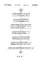
- FIG. 5 is a flow diagram summarizing the procedure for measuring the reference and calibration sample.
- FIG. 6 is a flow diagram outlining the procedure for measuring a sample of unknown film thickness.
- FIG. 1 Illustrated in FIG. 1 is a spectrophotometer system comprising an energy source 10 for generating light of wavelength ⁇ which is directed by a dichroic beam splitter 12 through an objective lens 14 to a sample 16. The image of the sample is then magnified by the the objective and the beam passes through the beam splitter and is focused on a monochromator 18 where the intensity of a narrow band of wavelengths is measured and is recorded by a computer 20 in its memory.
- an energy source 10 for generating light of wavelength ⁇ which is directed by a dichroic beam splitter 12 through an objective lens 14 to a sample 16.
- the image of the sample is then magnified by the the objective and the beam passes through the beam splitter and is focused on a monochromator 18 where the intensity of a narrow band of wavelengths is measured and is recorded by a computer 20 in its memory.
- n l complex refractive index of film
- n 0 complex refractive index of substrate
- Reflectance, R is computed by:
- Rho are all complex numbers with Rho being the complex reflectance.
- Reflectance, R is real.
- the system Before the system can measure the unknown film thickness of any sample, it must take reflectance measurements of both a reference sample and a calibration sample. These measurements are then used to obtain a theoretical model of reflectance which matches measured reflectance from samples with scatter much better than a model assuming perfect specular reflectance.
- the system illustrated in FIG. 1 performs the following operations at each wavelength of interest:
- the system first computes and stores in memory the theoretical reflectance, RTr, of the reference sample.
- This must be a sample whose measured reflectance closely matches that of the theoretical model and may be a bare substrate or have a film on the surface of a substrate.
- the important requirement is that the measured reflectance of the reference sample matches the theoretical reflectance. Silicon is a good choice since much is known and has been published about the properties of silicon.
- the system measures and stores in memory the raw intensity, Ir, of the reference sample. All optical elements in the optical system of FIG. 1 absorb energy from the radiating source 10 thereby requiring calibration of the system. This is done by dividing the measured raw intensity of the sample by that of a known reference to normalize the data so that it is independent of the efficiencies of the various components.
- the system of FIG. 1 measures, computes and stores in memory the theoretical real reflectance, RTc, and the theoretical complex reflectance, RhoTc, of the calibration sample.
- This calibration sample should be comprised of the same film and substrate materials and have the same scatter characteristics as those samples whose unknown film thicknesses will ultimately be measured by the system.
- RTc and RhoTc are computed assuming no scatter.
- the raw intensity, Ic, of the calibration sample is then measured and stored in memory.
- the computer computes and stores in memory the measured real reflectance, RMc, of the calibration sample:
- RMc is the absolute reflectance of the calibration sample.
- the absolute reflectance of any unknown sample may be measured, regardless of its film and substrate composition.
- ratio RMc/RTc gives the relative measure of the amount of scatter in the calibration sample compared to to an ideal non-scattering sample.
- the computer 20 in the system of FIG. 1 then computes and stores in memory the measured complex reflectance, RhoMc, of the calibration sample. ##EQU1##
- This new value for r 0 represents the Fresnel amplitude coefficient which has been adjusted from its original theoretical value (from Eq 2) in order to produce a new reflectance model which accounts for scatter, and is summarized in FIG. 5.
- This new value for r 0 is stored in memory and is used in the measurements of other samples. For example, the system of FIG. 1 may make measurements that may then be used with standard curve fitting methods to determine thickness of the thin film on a substrate, a measurement that is impossible without correcting for scatter.
- the system of FIG. 1 measures and stores in memory the raw intensity, Ix, of the unknown sample.
- the system then computes and stores in memory the unknown sample reflectance, Rx.
- the system computes the value of film thickness which results in the best fit of the unknown sample reflectance, Rx, to the theoretical sample reflectance Rm, (from Eqs. 5 and 7).
- the model reflectance computation uses the new value of r 0 , resulting in a much better fit of sample to model, compared to the fit obtained with the original value of r 0 , and a more accurate measure of film thickness.
- the system displays the computed value of film thickness.
Abstract
Description
r.sub.l =(1-n.sub.l)/(1+n.sub.l) (1)
r.sub.0 =(n.sub.l -n.sub.0)/(n.sub.l +n.sub.0) (2)
X=4πn.sub.l d/λ (3)
Rho=(r.sub.l +r.sub.0 * exp(i*X))/(1+r.sub.l *r.sub.0 *exp(i*X))(4)
R=|Rho|.sup.2 (R=magnitude squared of Rho)(5)
RMc=(Ic/Ir ) * RTr (6)
r.sub.0 =(r.sub.l -RhoMc)/(RhoMc * r.sub.l -1) * (exp(i*X))(8)
Claims (1)
Priority Applications (1)
| Application Number | Priority Date | Filing Date | Title |
|---|---|---|---|
| US08/035,291 US5452091A (en) | 1993-03-22 | 1993-03-22 | Scatter correction in reflectivity measurements |
Applications Claiming Priority (1)
| Application Number | Priority Date | Filing Date | Title |
|---|---|---|---|
| US08/035,291 US5452091A (en) | 1993-03-22 | 1993-03-22 | Scatter correction in reflectivity measurements |
Publications (1)
| Publication Number | Publication Date |
|---|---|
| US5452091A true US5452091A (en) | 1995-09-19 |
Family
ID=21881757
Family Applications (1)
| Application Number | Title | Priority Date | Filing Date |
|---|---|---|---|
| US08/035,291 Expired - Lifetime US5452091A (en) | 1993-03-22 | 1993-03-22 | Scatter correction in reflectivity measurements |
Country Status (1)
| Country | Link |
|---|---|
| US (1) | US5452091A (en) |
Cited By (31)
| Publication number | Priority date | Publication date | Assignee | Title |
|---|---|---|---|---|
| EP0800076A1 (en) * | 1996-04-04 | 1997-10-08 | The Boc Group, Inc. | Optical measuring systems |
| US5968690A (en) * | 1996-03-11 | 1999-10-19 | Vsli Technology, Inc. | Thin film thickness and optimal focus measuring using reflectivity |
| WO2001011310A1 (en) * | 1999-08-06 | 2001-02-15 | Thermo Biostar, Inc. | Instruments for analyzing binding assays based on attenuation of light by thin films |
| US6297880B1 (en) | 1998-01-29 | 2001-10-02 | Therma-Wave, Inc. | Apparatus for analyzing multi-layer thin film stacks on semiconductors |
| US6304326B1 (en) | 1997-07-11 | 2001-10-16 | Therma-Wave, Inc. | Thin film optical measurement system and method with calibrating ellipsometer |
| US6713753B1 (en) | 2001-07-03 | 2004-03-30 | Nanometrics Incorporated | Combination of normal and oblique incidence polarimetry for the characterization of gratings |
| US20040070773A1 (en) * | 1998-04-21 | 2004-04-15 | Takenori Hirose | Thin film thickness measuring method and apparatus, and mehtod and apparatus for manufacturing a thin film device using the same |
| US6795184B1 (en) | 2001-04-06 | 2004-09-21 | J.A. Woollam Co., Inc | Odd bounce image rotation system in ellipsometer systems |
| US20040263850A1 (en) * | 2003-06-25 | 2004-12-30 | Guoguang Li | Method and apparatus for examining features on semi-transparent and transparent substrates |
| US20050151969A1 (en) * | 2004-01-14 | 2005-07-14 | Taiwan Semiconductor Manufacturing Co. | Approach to improve ellipsometer modeling accuracy for solving material optical constants N & K |
| US20070181794A1 (en) * | 2004-08-11 | 2007-08-09 | Phillip Walsh | Method and apparatus for accurate calibration of a reflectometer by using a relative reflectance measurement |
| US20070182970A1 (en) * | 2004-08-11 | 2007-08-09 | Harrison Dale A | Method and apparatus for performing highly accurate thin film measurements |
| US20070181793A1 (en) * | 2004-08-11 | 2007-08-09 | Harrison Dale A | Method and apparatus for accurate calibration of VUV reflectometer |
| US20070181795A1 (en) * | 2004-08-11 | 2007-08-09 | Phillip Walsh | Method and apparatus for accurate calibration of a reflectometer by using a relative reflectance measurement |
| US20070215801A1 (en) * | 2004-08-11 | 2007-09-20 | Phillip Walsh | Method and apparatus for accurate calibration of a reflectometer by using a relative reflectance measurement |
| US20090219537A1 (en) * | 2008-02-28 | 2009-09-03 | Phillip Walsh | Method and apparatus for using multiple relative reflectance measurements to determine properties of a sample using vacuum ultra violet wavelengths |
| US20100051822A1 (en) * | 2003-01-16 | 2010-03-04 | Metrosol, Inc. | Broad band referencing reflectometer |
| US20100177324A1 (en) * | 2006-11-30 | 2010-07-15 | Metrosol, Inc. | Method and apparatus for optically measuring periodic structures using orthogonal azimuthal sample orientation |
| US20100277741A1 (en) * | 2007-04-09 | 2010-11-04 | Jordan Valley Semiconductors Ltd. | Combined optical metrology techniques |
| US20100290033A1 (en) * | 2003-01-16 | 2010-11-18 | Jordan Valley Semiconductors Ltd. | Method and System for Using Reflectometry Below Deep Ultra-Violet (DUV) Wavelengths for Measuring Properties of Diffracting or Scattering Structures on Substrate Work Pieces |
| US20100294922A1 (en) * | 2009-05-22 | 2010-11-25 | Hurst Jeffrey B | Automated calibration methodology for VUV metrology system |
| US8169611B2 (en) | 2009-02-27 | 2012-05-01 | University Of Nebraska Board Of Regents | Terahertz-infrared ellipsometer system, and method of use |
| US8416408B1 (en) | 2009-02-27 | 2013-04-09 | J.A. Woollam Co., Inc. | Terahertz-infrared ellipsometer system, and method of use |
| US8488119B2 (en) | 2009-02-27 | 2013-07-16 | J.A. Woollam Co., Inc. | Terahertz-infrared ellipsometer system, and method of use |
| US8565379B2 (en) | 2011-03-14 | 2013-10-22 | Jordan Valley Semiconductors Ltd. | Combining X-ray and VUV analysis of thin film layers |
| US8564777B1 (en) | 2010-08-16 | 2013-10-22 | J.A. Woollam Co., Inc. | System and method for compensating detector non-idealities |
| US20140118751A1 (en) * | 2012-10-26 | 2014-05-01 | Applied Materials, Inc. | Pecvd process |
| US8736838B2 (en) | 2009-02-27 | 2014-05-27 | J.A. Woollam Co., Inc. | Terahertz ellipsometer system, and method of use |
| US8867041B2 (en) | 2011-01-18 | 2014-10-21 | Jordan Valley Semiconductor Ltd | Optical vacuum ultra-violet wavelength nanoimprint metrology |
| US8934096B2 (en) | 2009-02-27 | 2015-01-13 | University Of Nebraska Board Of Regents | Terahertz-infrared ellipsometer system, and method of use |
| WO2016102938A1 (en) * | 2014-12-22 | 2016-06-30 | Ndc Infrared Engineering Limited | Measurement of porous film |
Citations (4)
| Publication number | Priority date | Publication date | Assignee | Title |
|---|---|---|---|---|
| US4350442A (en) * | 1976-05-19 | 1982-09-21 | Accusort Corporation | Light and color detecting scanner for a sorting apparatus |
| US4680084A (en) * | 1984-08-21 | 1987-07-14 | American Telephone And Telegraph Company, At&T Bell Laboratories | Interferometric methods and apparatus for device fabrication |
| US4766551A (en) * | 1986-09-22 | 1988-08-23 | Pacific Scientific Company | Method of comparing spectra to identify similar materials |
| US4899055A (en) * | 1988-05-12 | 1990-02-06 | Tencor Instruments | Thin film thickness measuring method |
-
1993
- 1993-03-22 US US08/035,291 patent/US5452091A/en not_active Expired - Lifetime
Patent Citations (4)
| Publication number | Priority date | Publication date | Assignee | Title |
|---|---|---|---|---|
| US4350442A (en) * | 1976-05-19 | 1982-09-21 | Accusort Corporation | Light and color detecting scanner for a sorting apparatus |
| US4680084A (en) * | 1984-08-21 | 1987-07-14 | American Telephone And Telegraph Company, At&T Bell Laboratories | Interferometric methods and apparatus for device fabrication |
| US4766551A (en) * | 1986-09-22 | 1988-08-23 | Pacific Scientific Company | Method of comparing spectra to identify similar materials |
| US4899055A (en) * | 1988-05-12 | 1990-02-06 | Tencor Instruments | Thin film thickness measuring method |
Cited By (71)
| Publication number | Priority date | Publication date | Assignee | Title |
|---|---|---|---|---|
| US5968690A (en) * | 1996-03-11 | 1999-10-19 | Vsli Technology, Inc. | Thin film thickness and optimal focus measuring using reflectivity |
| US5982496A (en) * | 1996-03-11 | 1999-11-09 | Vlsi Technology, Inc. | Thin film thickness and optimal focus measuring using reflectivity |
| EP0800076A1 (en) * | 1996-04-04 | 1997-10-08 | The Boc Group, Inc. | Optical measuring systems |
| US6753962B2 (en) | 1997-07-11 | 2004-06-22 | Therma-Wave, Inc. | Thin film optical measurement system and method with calibrating ellipsometer |
| US6934025B2 (en) | 1997-07-11 | 2005-08-23 | Therma-Wave, Inc. | Thin film optical measurement system and method with calibrating ellipsometer |
| US20040207845A1 (en) * | 1997-07-11 | 2004-10-21 | Jon Opsal | Thin film optical measurement system and method with calibrating ellipsometer |
| US6304326B1 (en) | 1997-07-11 | 2001-10-16 | Therma-Wave, Inc. | Thin film optical measurement system and method with calibrating ellipsometer |
| US6411385B2 (en) | 1997-07-11 | 2002-06-25 | Therma-Wave, Inc. | Thin film optical measurement system and method with calibrating ellipsometer |
| US6515746B2 (en) | 1997-07-11 | 2003-02-04 | Therma-Wave, Inc. | Thin film optical measurement system and method with calibrating ellipsometer |
| US6774997B2 (en) | 1998-01-29 | 2004-08-10 | Therma-Wave, Inc. | Apparatus for analyzing multi-layer thin film stacks on semiconductors |
| US6922244B2 (en) | 1998-01-29 | 2005-07-26 | Therma-Wave, Inc. | Thin film optical measurement system and method with calibrating ellipsometer |
| US6567213B2 (en) | 1998-01-29 | 2003-05-20 | Therma-Wave, Inc. | Apparatus for analyzing multi-layer thin film stacks on semiconductors |
| US6417921B2 (en) | 1998-01-29 | 2002-07-09 | Therma-Wave, Inc. | Apparatus for analyzing multi-layer thin film stacks on semiconductors |
| US6297880B1 (en) | 1998-01-29 | 2001-10-02 | Therma-Wave, Inc. | Apparatus for analyzing multi-layer thin film stacks on semiconductors |
| US20040070773A1 (en) * | 1998-04-21 | 2004-04-15 | Takenori Hirose | Thin film thickness measuring method and apparatus, and mehtod and apparatus for manufacturing a thin film device using the same |
| US6753972B1 (en) * | 1998-04-21 | 2004-06-22 | Hitachi, Ltd. | Thin film thickness measuring method and apparatus, and method and apparatus for manufacturing a thin film device using the same |
| US6806970B2 (en) | 1998-04-21 | 2004-10-19 | Hitachi, Ltd. | Thin film thickness measuring method and apparatus, and method and apparatus for manufacturing a thin film device using the same |
| WO2001011310A1 (en) * | 1999-08-06 | 2001-02-15 | Thermo Biostar, Inc. | Instruments for analyzing binding assays based on attenuation of light by thin films |
| US6795184B1 (en) | 2001-04-06 | 2004-09-21 | J.A. Woollam Co., Inc | Odd bounce image rotation system in ellipsometer systems |
| US6713753B1 (en) | 2001-07-03 | 2004-03-30 | Nanometrics Incorporated | Combination of normal and oblique incidence polarimetry for the characterization of gratings |
| US8054453B2 (en) | 2003-01-16 | 2011-11-08 | Jordan Valley Semiconductors Ltd. | Broad band referencing reflectometer |
| US8564780B2 (en) | 2003-01-16 | 2013-10-22 | Jordan Valley Semiconductors Ltd. | Method and system for using reflectometry below deep ultra-violet (DUV) wavelengths for measuring properties of diffracting or scattering structures on substrate work pieces |
| US8014000B2 (en) | 2003-01-16 | 2011-09-06 | Jordan Valley Semiconductors Ltd. | Broad band referencing reflectometer |
| US20100328648A1 (en) * | 2003-01-16 | 2010-12-30 | Jordan Valley Semiconductors Ltd. | Broad band referencing reflectometer |
| US20100290033A1 (en) * | 2003-01-16 | 2010-11-18 | Jordan Valley Semiconductors Ltd. | Method and System for Using Reflectometry Below Deep Ultra-Violet (DUV) Wavelengths for Measuring Properties of Diffracting or Scattering Structures on Substrate Work Pieces |
| US20100051822A1 (en) * | 2003-01-16 | 2010-03-04 | Metrosol, Inc. | Broad band referencing reflectometer |
| US6891628B2 (en) * | 2003-06-25 | 2005-05-10 | N & K Technology, Inc. | Method and apparatus for examining features on semi-transparent and transparent substrates |
| US7253909B1 (en) * | 2003-06-25 | 2007-08-07 | N&K Technology, Inc. | Phase shift measurement using transmittance spectra |
| US20040263850A1 (en) * | 2003-06-25 | 2004-12-30 | Guoguang Li | Method and apparatus for examining features on semi-transparent and transparent substrates |
| US20050151969A1 (en) * | 2004-01-14 | 2005-07-14 | Taiwan Semiconductor Manufacturing Co. | Approach to improve ellipsometer modeling accuracy for solving material optical constants N & K |
| US7259850B2 (en) * | 2004-01-14 | 2007-08-21 | Taiwan Semiconductor Manufacturing Company | Approach to improve ellipsometer modeling accuracy for solving material optical constants N & K |
| US7663097B2 (en) | 2004-08-11 | 2010-02-16 | Metrosol, Inc. | Method and apparatus for accurate calibration of a reflectometer by using a relative reflectance measurement |
| US20070181793A1 (en) * | 2004-08-11 | 2007-08-09 | Harrison Dale A | Method and apparatus for accurate calibration of VUV reflectometer |
| US8119991B2 (en) | 2004-08-11 | 2012-02-21 | Jordan Valley Semiconductors Ltd. | Method and apparatus for accurate calibration of VUV reflectometer |
| US7399975B2 (en) * | 2004-08-11 | 2008-07-15 | Metrosol, Inc. | Method and apparatus for performing highly accurate thin film measurements |
| US7282703B2 (en) | 2004-08-11 | 2007-10-16 | Metrosol, Inc. | Method and apparatus for accurate calibration of a reflectometer by using a relative reflectance measurement |
| US7511265B2 (en) | 2004-08-11 | 2009-03-31 | Metrosol, Inc. | Method and apparatus for accurate calibration of a reflectometer by using a relative reflectance measurement |
| US7804059B2 (en) * | 2004-08-11 | 2010-09-28 | Jordan Valley Semiconductors Ltd. | Method and apparatus for accurate calibration of VUV reflectometer |
| US20070182970A1 (en) * | 2004-08-11 | 2007-08-09 | Harrison Dale A | Method and apparatus for performing highly accurate thin film measurements |
| US20070215801A1 (en) * | 2004-08-11 | 2007-09-20 | Phillip Walsh | Method and apparatus for accurate calibration of a reflectometer by using a relative reflectance measurement |
| US20070181794A1 (en) * | 2004-08-11 | 2007-08-09 | Phillip Walsh | Method and apparatus for accurate calibration of a reflectometer by using a relative reflectance measurement |
| US20100301225A1 (en) * | 2004-08-11 | 2010-12-02 | Jordan Valley Semiconductors Ltd. | Method and Apparatus for Accurate Calibration of VUV Reflectometer |
| US20070181795A1 (en) * | 2004-08-11 | 2007-08-09 | Phillip Walsh | Method and apparatus for accurate calibration of a reflectometer by using a relative reflectance measurement |
| US20100177324A1 (en) * | 2006-11-30 | 2010-07-15 | Metrosol, Inc. | Method and apparatus for optically measuring periodic structures using orthogonal azimuthal sample orientation |
| US7990549B2 (en) | 2006-11-30 | 2011-08-02 | Jordan Valley Semiconductors Ltd. | Method and apparatus for optically measuring periodic structures using orthogonal azimuthal sample orientation |
| US20100277741A1 (en) * | 2007-04-09 | 2010-11-04 | Jordan Valley Semiconductors Ltd. | Combined optical metrology techniques |
| US7948631B2 (en) | 2008-02-28 | 2011-05-24 | Jordan Valley Semiconductors Ltd. | Method and apparatus for using multiple relative reflectance measurements to determine properties of a sample using vacuum ultra violet wavelengths |
| US20090219537A1 (en) * | 2008-02-28 | 2009-09-03 | Phillip Walsh | Method and apparatus for using multiple relative reflectance measurements to determine properties of a sample using vacuum ultra violet wavelengths |
| US8416408B1 (en) | 2009-02-27 | 2013-04-09 | J.A. Woollam Co., Inc. | Terahertz-infrared ellipsometer system, and method of use |
| US8736838B2 (en) | 2009-02-27 | 2014-05-27 | J.A. Woollam Co., Inc. | Terahertz ellipsometer system, and method of use |
| US9121757B2 (en) | 2009-02-27 | 2015-09-01 | J.A. Woollam Co., Inc. | Terahertz ellipsometer system, and method of use |
| US8488119B2 (en) | 2009-02-27 | 2013-07-16 | J.A. Woollam Co., Inc. | Terahertz-infrared ellipsometer system, and method of use |
| US9041927B1 (en) | 2009-02-27 | 2015-05-26 | J.A. Woollam Co., Inc | Terahertz-infrared ellipsometer system, and method of use |
| US8934096B2 (en) | 2009-02-27 | 2015-01-13 | University Of Nebraska Board Of Regents | Terahertz-infrared ellipsometer system, and method of use |
| US8169611B2 (en) | 2009-02-27 | 2012-05-01 | University Of Nebraska Board Of Regents | Terahertz-infrared ellipsometer system, and method of use |
| US8705032B2 (en) | 2009-02-27 | 2014-04-22 | J.A. Woollam Co., Inc | Terahertz-infrared ellipsometer system, and method of use |
| US20100294922A1 (en) * | 2009-05-22 | 2010-11-25 | Hurst Jeffrey B | Automated calibration methodology for VUV metrology system |
| US8153987B2 (en) | 2009-05-22 | 2012-04-10 | Jordan Valley Semiconductors Ltd. | Automated calibration methodology for VUV metrology system |
| US8564777B1 (en) | 2010-08-16 | 2013-10-22 | J.A. Woollam Co., Inc. | System and method for compensating detector non-idealities |
| US8867041B2 (en) | 2011-01-18 | 2014-10-21 | Jordan Valley Semiconductor Ltd | Optical vacuum ultra-violet wavelength nanoimprint metrology |
| US8565379B2 (en) | 2011-03-14 | 2013-10-22 | Jordan Valley Semiconductors Ltd. | Combining X-ray and VUV analysis of thin film layers |
| US20140118751A1 (en) * | 2012-10-26 | 2014-05-01 | Applied Materials, Inc. | Pecvd process |
| US9157730B2 (en) * | 2012-10-26 | 2015-10-13 | Applied Materials, Inc. | PECVD process |
| WO2016102938A1 (en) * | 2014-12-22 | 2016-06-30 | Ndc Infrared Engineering Limited | Measurement of porous film |
| KR20170102264A (en) * | 2014-12-22 | 2017-09-08 | 엔디씨 테크놀로지스 리미티드 | Measurement of porous film |
| CN107430054A (en) * | 2014-12-22 | 2017-12-01 | Ndc技术有限公司 | The measurement of perforated membrane |
| US10161863B2 (en) | 2014-12-22 | 2018-12-25 | Ndc Technologies Limited | Measurement of porous film |
| CN107430054B (en) * | 2014-12-22 | 2020-04-17 | Ndc技术有限公司 | Measurement of porous membranes |
| JP2020106536A (en) * | 2014-12-22 | 2020-07-09 | エヌディーシー テクノロジーズ リミテッド | Measurement of porous film |
| KR102172593B1 (en) | 2014-12-22 | 2020-11-02 | 엔디씨 테크놀로지스 리미티드 | Measurement of porous film |
| JP2022024012A (en) * | 2014-12-22 | 2022-02-08 | エヌディーシー テクノロジーズ リミテッド | Measurement of porous film |
Similar Documents
| Publication | Publication Date | Title |
|---|---|---|
| US5452091A (en) | Scatter correction in reflectivity measurements | |
| EP0350869B1 (en) | Method of and apparatus for measuring film thickness | |
| KR970011746B1 (en) | Apparatus and method for measuring the thickness of thin films | |
| US4332476A (en) | Method and apparatus for studying surface properties | |
| US5291269A (en) | Apparatus and method for performing thin film layer thickness metrology on a thin film layer having shape deformations and local slope variations | |
| US6128085A (en) | Reflectance spectroscopic apparatus with toroidal mirrors | |
| US4872758A (en) | Film thickness-measuring apparatus | |
| US4999014A (en) | Method and apparatus for measuring thickness of thin films | |
| US6392756B1 (en) | Method and apparatus for optically determining physical parameters of thin films deposited on a complex substrate | |
| US5241366A (en) | Thin film thickness monitor | |
| US6522406B1 (en) | Correcting the system polarization sensitivity of a metrology tool having a rotatable polarizer | |
| US5337150A (en) | Apparatus and method for performing thin film layer thickness metrology using a correlation reflectometer | |
| US5880831A (en) | Reflectance spectrophotometric apparatus with optical relay | |
| US8319966B2 (en) | Optical metrology systems and methods | |
| EP0183831A1 (en) | Technique for measuring very small spacings | |
| US5526117A (en) | Method for the determination of characteristic values of transparent layers with the aid of ellipsometry | |
| US7158231B1 (en) | Spectroscopic ellipsometer and polarimeter systems | |
| US7505133B1 (en) | Optical metrology systems and methods | |
| Levins et al. | Extended spectral analysis of multiple beam interferometry: a technique to study metallic films in the surface forces apparatus | |
| US5717490A (en) | Method for identifying order skipping in spectroreflective film measurement equipment | |
| JP3000303B2 (en) | Method and apparatus for measuring optical constants and film thickness in vacuum deposition equipment | |
| JPH0643957B2 (en) | Refractive index dispersion measuring method and film thickness measuring method | |
| JP2992839B2 (en) | Method and apparatus for measuring optical constant and film thickness | |
| El-Zaiat et al. | Applying multiple-beam Fizeau fringes for measuring the refractive indices of liquids | |
| Carren et al. | Use of spectrogoniometric—ellipsometric techniques for the determination of optical properties of films of trinitrofluorenone and poly-n-vinylcarbazole |
Legal Events
| Date | Code | Title | Description |
|---|---|---|---|
| STPP | Information on status: patent application and granting procedure in general |
Free format text: APPLICATION UNDERGOING PREEXAM PROCESSING |
|
| AS | Assignment |
Owner name: NANOMETRICS INCORPORATED, CALIFORNIA Free format text: ASSIGNMENT OF ASSIGNORS INTEREST;ASSIGNOR:JOHNSON, RODNEY P.;REEL/FRAME:007620/0352 Effective date: 19950530 |
|
| FPAY | Fee payment |
Year of fee payment: 4 |
|
| FPAY | Fee payment |
Year of fee payment: 8 |
|
| FEPP | Fee payment procedure |
Free format text: PAT HOLDER NO LONGER CLAIMS SMALL ENTITY STATUS, ENTITY STATUS SET TO UNDISCOUNTED (ORIGINAL EVENT CODE: STOL); ENTITY STATUS OF PATENT OWNER: LARGE ENTITY |
|
| REFU | Refund |
Free format text: REFUND - PAYMENT OF MAINTENANCE FEE, 12TH YR, SMALL ENTITY (ORIGINAL EVENT CODE: R2553); ENTITY STATUS OF PATENT OWNER: LARGE ENTITY |
|
| FPAY | Fee payment |
Year of fee payment: 12 |