US5474648A - Uniform and repeatable plasma processing - Google Patents
Uniform and repeatable plasma processing Download PDFInfo
- Publication number
- US5474648A US5474648A US08/283,296 US28329694A US5474648A US 5474648 A US5474648 A US 5474648A US 28329694 A US28329694 A US 28329694A US 5474648 A US5474648 A US 5474648A
- Authority
- US
- United States
- Prior art keywords
- plasma
- radio frequency
- processing system
- electrode
- plasma chamber
- Prior art date
- Legal status (The legal status is an assumption and is not a legal conclusion. Google has not performed a legal analysis and makes no representation as to the accuracy of the status listed.)
- Expired - Lifetime
Links
Images


Classifications
-
- H—ELECTRICITY
- H01—ELECTRIC ELEMENTS
- H01J—ELECTRIC DISCHARGE TUBES OR DISCHARGE LAMPS
- H01J37/00—Discharge tubes with provision for introducing objects or material to be exposed to the discharge, e.g. for the purpose of examination or processing thereof
- H01J37/32—Gas-filled discharge tubes
- H01J37/32009—Arrangements for generation of plasma specially adapted for examination or treatment of objects, e.g. plasma sources
- H01J37/32082—Radio frequency generated discharge
- H01J37/32174—Circuits specially adapted for controlling the RF discharge
- H01J37/32183—Matching circuits
-
- H—ELECTRICITY
- H01—ELECTRIC ELEMENTS
- H01J—ELECTRIC DISCHARGE TUBES OR DISCHARGE LAMPS
- H01J37/00—Discharge tubes with provision for introducing objects or material to be exposed to the discharge, e.g. for the purpose of examination or processing thereof
- H01J37/32—Gas-filled discharge tubes
- H01J37/32917—Plasma diagnostics
- H01J37/32935—Monitoring and controlling tubes by information coming from the object and/or discharge
- H01J37/32963—End-point detection
-
- H—ELECTRICITY
- H01—ELECTRIC ELEMENTS
- H01J—ELECTRIC DISCHARGE TUBES OR DISCHARGE LAMPS
- H01J37/00—Discharge tubes with provision for introducing objects or material to be exposed to the discharge, e.g. for the purpose of examination or processing thereof
- H01J37/32—Gas-filled discharge tubes
- H01J37/32917—Plasma diagnostics
- H01J37/3299—Feedback systems
-
- H—ELECTRICITY
- H01—ELECTRIC ELEMENTS
- H01J—ELECTRIC DISCHARGE TUBES OR DISCHARGE LAMPS
- H01J2237/00—Discharge tubes exposing object to beam, e.g. for analysis treatment, etching, imaging
- H01J2237/32—Processing objects by plasma generation
- H01J2237/33—Processing objects by plasma generation characterised by the type of processing
- H01J2237/332—Coating
-
- H—ELECTRICITY
- H01—ELECTRIC ELEMENTS
- H01J—ELECTRIC DISCHARGE TUBES OR DISCHARGE LAMPS
- H01J2237/00—Discharge tubes exposing object to beam, e.g. for analysis treatment, etching, imaging
- H01J2237/32—Processing objects by plasma generation
- H01J2237/33—Processing objects by plasma generation characterised by the type of processing
- H01J2237/334—Etching
Definitions
- the present invention relates to plasma processing systems and, more particularly, to a method and apparatus for dynamically controlling the delivery of radio frequency power in plasma process systems.
- Ionized gas or "plasma” may be used during processing and fabrication of semiconductor devices, flat panel displays and in other industries requiring etching or deposition of materials.
- Plasma may be used to etch or remove material from semiconductor integrated circuit wafers, sputter or deposit material onto a semiconducting, conducting or insulating surface.
- Creating a plasma for use in manufacturing or fabrication processes typically, is done by introducing a low pressure process gas into a process vessel chamber surrounding a work piece such as an integrated circuit wafer.
- the molecules of the low pressure gas in the chamber are ionized into a plasma by the radio frequency energy (power) source after entering the chamber, and the highly reactive plasma flows over the work piece.
- the process vessel is used to maintain the low pressures required for the plasma and to serve as a structure for attachment of one or more radio frequency energy sources.
- Plasma may be created from a low pressure process gas by inducing an electron flow which ionizes individual gas molecules by the transfer of kinetic energy through individual electron-gas molecule collisions.
- electrons are accelerated in an electric field such as one produced by radio frequency ("RF") energy.
- RF radio frequency
- This RF energy may be low frequencies (below 550 KHz), high frequencies (13.56 MHz), or microwaves (2.45 GHz).
- a plasma etching system consists of a radio frequency energy source and a pair of electrodes. A plasma is generated between the electrodes while the work piece, such as a semiconductor wafer, is planar with one of the electrodes. The chemical species in the plasma are determined by the source gas(es) used.
- a typical plasma etching system may consist of an enclosure having an interior bounded at least in part by a radio frequency transparent window.
- a planar coil is disposed proximate to the window, and a radio frequency energy source is coupled through an impedance matching circuit to the coil.
- the planar coil radiates the radio frequency energy such that a planar magnetic field is induced in the interior of the enclosure.
- a plasma is generated thereby from the process gas. This plasma reacts with the surface of the semiconductor wafer, etching it away.
- Plasma may also be used in chemical vapor deposition (CVD) to form thin films of metals, semiconductor or insulator materials onto a work piece such as a semiconductor wafer.
- CVD chemical vapor deposition
- Plasma-enhanced CVD uses the plasma to supply the required reaction energy for deposition of the desired materials.
- radio frequency energy is used to produce this plasma.
- Control and delivery of the power in a plasma discharge is of fundamental importance in plasma processing, including etching, sputtering and deposition systems. Uniformity and repeatability are critical aspects of plasma etching. Uniformity of the plasma is required in order to uniformly remove a desired layer from a semiconductor wafer while minimizing the undesired etching of an underlaying layer. Repeatability of the plasma etching process allows for increased manufacturing yields and a wider latitude in the manufacturing process tolerances.
- the most commonly used method of obtaining a predetermined radio frequency power is to use a matching network between a radio frequency power source and the plasma discharge chamber electrode or coupling coil.
- the matching network transforms the impedance (capacitive reactance) of the plasma discharge into a substantially resistive load for the radio frequency power source.
- the power source is then set to a predetermined power level dependent upon the process parameters desired.
- radio frequency power is monitored and controlled at the generator output on the assumption that the power losses in the matching network are negligible.
- radio frequency power delivered to the plasma chamber has been found to be substantially less than the generator power because of losses in the matching network and other associated components of the radio frequency power generation system.
- the amount of actual power in the plasma chamber greatly affects the process conditions. Significant variance in actual power delivered to the plasma chamber may unexpectedly change the anticipated contribution of other process variable parameters, such as pressure and etch rate.
- Plasma processes are characterized and ultimately optimized by evaluating the process results on a work piece such as, for example, a semiconductor wafer.
- the process results may be characterized as a function of the plasma process parameters, e.g., radio frequency power, plasma gas pressure, plasma chamber electrode spacing, types of gases uses to form the plasma, and the gas flow rates.
- Use of Response Surface Modeling (RSM) may be employed not only to find the optimum process performance but also to find the most stable plasma etching regions in order to reduce noise errors in the process.
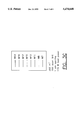
- the variation in etch rate over time for a plurality of semiconductor device wafers is graphically illustrated.
- the dots on the horizontal axis represent the plurality of wafers being etched and the vertical axis represents the respective etch rate for each of the plurality of wafers. A significant spread in the etch rate of the wafers can be noted.
- etch rate spread is significant because present art plasma etching tools such as the LAM TCP 9400 manufactured by Lam Research Corporation, Fremont, Calif., utilizes static control of the power to the plasma chamber.
- plasma etching process is a dynamic process, where most of the dynamics are in the first few seconds of the gas discharge, when the plasma stabilizes.
- Measuring and controlling the radio frequency power at the plasma chamber electrodes does not eliminate all of the non-uniformities and the wide variance (spread) in the etch rates between semiconductor wafers sequentially processed in the plasma chamber. It has been determined that the remaining non-uniformities and the spread in the etch rates are caused substantially by the way the plasma gas discharge is started.
- the plasma discharge is unstable during the first few seconds of the gas becoming a plasma. The plasma instability during these first few seconds causes more of the etch non-uniformities and spread in the etch rates than does the bulk etch time when the plasma is stable.
- FIGS. 3A and 3B illustrate the power taken by the plasma load as a function of time for a plurality of wafers, e.g., W7, W8, W11, W13, W15, W17, W19 and W23 (FIG. 3C).
- the load power versus time required during the start of the processing for each wafer is different (FIG. 3B is an expanded scale of FIG. 3A). It is this difference that has such a significant effect on the overall uniformity (or lack thereof) of the etch process for each wafer.
- What is needed is a way to optimize the plasma process during the first few seconds of creating a plasma from the gas by the application of the radio frequency power. It is therefore an object of the present invention to dynamically optimize the etching process during the formation (start) of the plasma.
- the present invention provides a system and method for dynamically controlling the radio frequency power parameters being delivered to a plasma chamber in order to optimize the formation of the plasma gas with a resulting increase in the repeatability and uniformity of the etching process.
- the present invention accomplishes this object by monitoring the power of the radio frequency energy being delivered to the plasma chamber, and dynamically controlling the radio frequency energy with a computer system.
- the voltage, current, phase and impedance of the plasma chamber electrode may also be measured and the measurement information used by the computer power control system of the present invention.
- FIGS. 2A and 2B A control system that monitors and controls the radio frequency power at the plasma chamber electrode is illustrated in FIGS. 2A and 2B.
- This radio frequency power control system includes a radio frequency sensor placed closely to the plasma load electrodes in the plasma etching chamber. This closely placed sensor provides signals to a power controller which, in turn, controls a radio frequency power generator. By controlling the amount of power at the plasma electrode instead of at the output of the generator, a number of errors, created by the variable process parameters and typically affecting the process accuracy of the radio frequency plasma system, are eliminated.
- Some of these process variable errors are: a) radio frequency generator forward power sensor accuracy, b) radio frequency generator forward power sensor load dependance, c) transmission line attenuation, d) matching network tuning window, e) and matching network losses (non-linear).
- a radio frequency matching network is connected between the output of a radio frequency power generator and a plasma chamber electrode such as, for example, a plate electrode or a planar coil.
- a radio frequency power sensor adjacent to the chamber electrode accurately measures the actual radio frequency power being delivered to the plasma chamber.
- the sensor may also measure the voltage, current and phase angle at the chamber electrode, and measure the chamber impedance as desired.
- a radio frequency circulator is connected to the output of a radio frequency power generator.
- the circulator is used to pass the radio frequency power to a plasma chamber electrode such as, for example, a plate electrode or a planar coil.
- a sensor between the circulator and chamber electrode measures the radio frequency power being delivered to the plasma chamber.
- the sensor measures the voltage, current and phase angle at the chamber electrode, and measures the chamber impedance as discussed above.
- the power sensor connects to a computer controlled power controller that controls the output power of the radio frequency power generator as described above.
- the purpose of the circulator is to minimize the amount of reflected power and generated harmonics from the plasma chamber electrode back to the generator.
- a circulator is a three port device that allows radio frequency power to flow in substantially one direction only. By connecting a terminating resistor to the circulator, the reflected power and generated harmonics from the plasma chamber electrode are absorbed and dissipated in this resistor.
- This embodiment of the present invention comprises a simple radio frequency power delivery system for use in a plasma generating system without complex mechanical and electrical matching circuits.
- the power sensor connects to a computer power controller that uses the sensor information to dynamically and pro-actively control the output power of the radio frequency power generator so that a desired power profile over time is available at the chamber electrode.
- the computer power controller may be programmed so that a desired process power profile is selectable for each type of process gas and/or work piece. The power profile is selected to obtain optimal plasma characteristics during the etching process.
- the power controller of the present invention utilizes a computer system and software to dynamically control the ramp up time, power overshoot, delay times, etc. of the radio frequency power delivered to the plasma chamber electrodes during the first few seconds of the initiation of the plasma process.
- the computer system may continue to control the radio frequency power during the entire plasma etching process. Etch rate and uniformity of etch may be more closely controlled by dynamically controlling the radio frequency power etch process parameters during formation of the plasma.
- dynamic control and optimization could also be implemented by other measurement devices such as, for example, microwave interferometers and optical emission spectrometers.
- the present invention contemplates controlling other process parameters, in addition to power, such as, for example, plasma gas flow or pressure.
- FIGS. 4A and 4B illustrate test results of the etch rates obtained with a static power control system (Lam) and the dynamic computer controlled system (AE) of the present invention.
- a wide variance (spread) is illustrated in FIGS. 4A and 4B for the static power control system (Lam), while the dynamic control system (AE) of the present invention is significantly more uniform for each wafer.
- Greatly improved etch rate consistency and uniformity are illustrated in FIGS. 4A and 4B, respectively, when utilizing the system and method of the present invention.
- FIGS. 5A and 5B illustrate the dynamic power control of the present invention that improves the etch uniformity. It is understood to those of ordinary skill in the art of plasma etching that the optimized power delivery for different gas chemistries may have significantly different characteristics. Furthermore, it may be advantageous to control one or more of the other electrical parameters of the plasma electrodes such as, for example, the electrode voltage. There are instances when the voltage across the work piece in the plasma chamber can exceed about 350 volts instead of the more typical 110 volts. This excess electrode voltage can severely damage the devices on the work piece semiconductor wafer or corrupt the film on liquid crystal displays. By dynamically controlling the plasma etch parameters, much of the unwanted plasma characteristics may be eliminated.
- the computer control system of the present invention may also monitor the plasma chamber electrode load characteristics so that detection of chamber leaks may be determined.
- a chamber leak occurs when air enters the plasma chamber during the low pressure gas plasma formation or operation.
- a properly operating plasma chamber will have a well defined electrode load that may be characterized by the radio frequency parameter sensor. If an unwanted leak occurs at least some of the electrode load parameters will change. These unexpected changes may be detected by comparing the process to a process profile and noting any deviation so that an operator may alerted that the plasma process system is not functioning as expected. Contamination of the plasma chamber may also be detected in this manner because any contaminates affect the plasma etching process profile.
- An object of the present invention is to dynamically control the radio frequency power in a plasma etching process.
- Another object is to dynamically optimize the plasma etching process.
- Still another object is to improve the repeatability of the plasma etching process.
- a further object is to improve the uniformity of the plasma etching process.
- Another object of the present invention is to reduce over etch time, thus reducing damage to the work piece.
- Another object is to reduce etch time and improve process through put.
- Still another object is to increase the parameter range for a desired process characteristic.
- Another object is to reduce plasma etching process fabrication costs by reducing process variations.
- Another object is to minimize overshoot of radio frequency induced plasma process parameters so as to reduce damage to the work piece.
- An advantage of the present invention is more uniform processing of semiconductor wafers.
- Another advantage is preventing excessive voltages from degrading work pieces in the plasma chamber.
- Another advantage is starting a plasma with an optimal radio frequency power value so that the resulting plasma characteristics are substantially the same as the characteristics of plasmas in similar plasma processes.
- a feature of the present invention is the use of a computer and software program for dynamically controlling the radio frequency power to a plasma chamber electrode.
- Another feature is control of the maximum voltage potential on the work piece.
- Still another feature is control of the maximum current flow in the work piece.
- FIG. 1 is a graph of etch rates for a plurality of wafers etched by a prior art etching process
- FIGS. 2A and 2B are schematic block diagrams of embodiments of the present invention.
- FIGS. 3A and 3B are graphs of the power taken by the different wafers noted in FIG. 3C;
- FIGS. 4A and 4B are graphs of the etch rates and uniformity percentage for both static and dynamic power control systems
- FIGS. 5A and 5B are graphs of dynamic load power control of the present invention.
- FIG. 6 is a schematic block flow diagram of the computer program of the present invention.
- a radio frequency (“RF") generator 102 is coupled to a plasma chamber 104 through a matching network 120 consisting of variable capacitors 106 and 108, and coil 110.
- the plasma chamber 104 includes electrodes 112 and 114.
- a semiconductor wafer 116 is in planar communication with the electrode 114.
- An RF excitation field is created between the electrodes 112 and 114, and when a process gas or gases (not illustrated) is introduced into the plasma chamber 104, the gas turns into a plasma. The plasma reactively etches the surface of the semiconductor wafer 116.
- Power sensor 202 measures the radio frequency power being delivered to the plasma chamber 104.
- a power controller 204 utilizes a signal representative of the measured power from the power sensor 202 to control the amount of power from the RF generator 102.
- Matching network 120 automatically adjusts to produce a match condition between the RF generator 102 and the plasma chamber 104.
- An advantage in measuring and controlling the power at the plasma chamber is that a more uniform and repeatable plasma process results because the widely varying power losses through the matching network 120 are no longer a factor.
- FIG. 2B a schematic block diagram of another preferred embodiment of the present invention for a system for plasma etching a semiconductor wafer is illustrated schematically.
- the output of RF generator 102 is connected to a radio frequency circulator 302.
- One output port 302a of the circulator 302 connects to the plasma chamber 104 through the power sensor 202.
- a termination resistor 304 connects to another port 302b of circulator 302.
- a termination resistor 304 absorbs substantially all of the reflected power caused by a high standing wave ratio ("SWR") and harmonics from the plasma chamber 104 reactive and non-linear impedance.
- SWR standing wave ratio
- circulator 302 The purpose of circulator 302 is to present a more uniform load 302c to the RF generator 102 without the need of an adjustable matching network 120 (FIG. 2A).
- Power to the plasma chamber 104 is monitored by power sensor 202 and closely controlled by means of the computer system RF power generator controller 204 which controls the output of the RF generator 102.
- Power from the generator 102 to the plasma chamber 104 is precisely controlled by the controller 204 without introducing unknown power losses caused by varying transfer efficiencies of the matching network 120 or circulator 302 when used over the range of impedance values presented during the plasma process.
- the computer system and radio frequency power generator controller 204 may be controlled by a computer and software program that dynamically determines the power delivered to the chamber 104 at any instant of time during the plasma etching process. Control profiles for each type of process gas and type of work piece may be stored in the software program. A plurality of different processes may be characterized and stored for subsequent commercial manufacturing of semiconductor wafers.
- An advantage in knowing the voltage, current, phase angle and impedance parameters of the plasma chamber enables better control of the plasma process parameters. These parameters may also be used to characterize any abnormality or deviation from a normally expected etching process. A chamber leak will result in a variance from the characteristic parameters as will contamination of the chamber. Once a desired process is characterized, all of the chamber parameters may be monitored to insure that each subsequent process is substantially uniform with the one before.
- Step 602 starts the plasma process and step 604 causes the computer system 204 to dynamically set the radio frequency power at the chamber electrode (112, 114) to a first desired power value as determined by the RF parameter sensor 202 in step 606.
- the program of step 608, controls the dynamic characteristics of the RF power profile to the chamber 104 so as to maximize the consistency and repeatability of the plasma characteristics for each subsequent process.
- the program of step 608 controls the ramp time, overshoot and time duration of the first desired power value applied to the chamber 104. Dynamically controlling the first desired power value substantially increases the uniformity of the plasma at the beginning of the process where uniformity is especially critical.
- the program of step 608 causes step 610 to set the RF power to a second desired power value after a predetermined time. This second desired power value may then be utilized during the remainder of the plasma etching process.
- Step 612 ends the process when a desired etch time is completed.
Abstract
Description
Claims (30)
Priority Applications (1)
| Application Number | Priority Date | Filing Date | Title |
|---|---|---|---|
| US08/283,296 US5474648A (en) | 1994-07-29 | 1994-07-29 | Uniform and repeatable plasma processing |
Applications Claiming Priority (1)
| Application Number | Priority Date | Filing Date | Title |
|---|---|---|---|
| US08/283,296 US5474648A (en) | 1994-07-29 | 1994-07-29 | Uniform and repeatable plasma processing |
Publications (1)
| Publication Number | Publication Date |
|---|---|
| US5474648A true US5474648A (en) | 1995-12-12 |
Family
ID=23085376
Family Applications (1)
| Application Number | Title | Priority Date | Filing Date |
|---|---|---|---|
| US08/283,296 Expired - Lifetime US5474648A (en) | 1994-07-29 | 1994-07-29 | Uniform and repeatable plasma processing |
Country Status (1)
| Country | Link |
|---|---|
| US (1) | US5474648A (en) |
Cited By (137)
| Publication number | Priority date | Publication date | Assignee | Title |
|---|---|---|---|---|
| EP0753876A2 (en) * | 1995-06-07 | 1997-01-15 | Eni, A Division Of Astec America, Inc. | Aliasing sampler for plasma probe detection |
| US5688357A (en) * | 1995-02-15 | 1997-11-18 | Applied Materials, Inc. | Automatic frequency tuning of an RF power source of an inductively coupled plasma reactor |
| US5779925A (en) * | 1994-10-14 | 1998-07-14 | Fujitsu Limited | Plasma processing with less damage |
| DE19737244A1 (en) * | 1997-08-27 | 1999-03-04 | Harald Tobies | Device and method for regulating the phase position of high-frequency electrodes in plasma processes |
| WO1999014699A1 (en) * | 1997-09-17 | 1999-03-25 | Tokyo Electron Limited | System and method for monitoring and controlling gas plasma processes |
| US5908791A (en) * | 1995-10-11 | 1999-06-01 | Samsung Electronics Co., Ltd. | Method of forming a polycide gate of a semiconductor device |
| US6041734A (en) * | 1997-12-01 | 2000-03-28 | Applied Materials, Inc. | Use of an asymmetric waveform to control ion bombardment during substrate processing |
| US6042686A (en) * | 1995-06-30 | 2000-03-28 | Lam Research Corporation | Power segmented electrode |
| US6056850A (en) * | 1996-07-12 | 2000-05-02 | Micron Technology, Inc. | Apparatus for improving the performance of a temperature-sensitive etch process |
| US6060837A (en) * | 1998-01-09 | 2000-05-09 | Lam Research Corporation | Method of and apparatus for minimizing plasma instability in an rf processor |
| US6098568A (en) * | 1997-12-01 | 2000-08-08 | Applied Materials, Inc. | Mixed frequency CVD apparatus |
| US6174450B1 (en) | 1997-04-16 | 2001-01-16 | Lam Research Corporation | Methods and apparatus for controlling ion energy and plasma density in a plasma processing system |
| DE19941542A1 (en) * | 1999-09-01 | 2001-03-08 | Aurion Anlagentechnik Gmbh | Automatic tuning method and device for HF impedance matching network for plasma process uses cyclic measurement of electrical parameters and adjustment of tuning components in alternation |
| US6255635B1 (en) | 1998-07-10 | 2001-07-03 | Ameritherm, Inc. | System and method for providing RF power to a load |
| US20010007778A1 (en) * | 1999-12-29 | 2001-07-12 | Winbond Electronics Corp. | Method and system of frequency modulated end-point detection |
| US6265831B1 (en) | 1999-03-31 | 2001-07-24 | Lam Research Corporation | Plasma processing method and apparatus with control of rf bias |
| US20020038688A1 (en) * | 2000-08-11 | 2002-04-04 | Alps Electric Co., Ltd. And Tadahiro Ohmi | Plasma processing apparatus and system, performance validation system and inspection method therefor |
| US20020068012A1 (en) * | 2000-10-02 | 2002-06-06 | Platt Robert C. | Sterilization system employing a switching module adapted to pulsate the low frequency power applied to a plasma |
| US20020088400A1 (en) * | 2000-11-08 | 2002-07-11 | Alps Electric Co., Ltd. | Plasma processing apparatus including a plurality of plasma processing units having reduced variation |
| US20020195330A1 (en) * | 2000-10-02 | 2002-12-26 | Mitch Agamohamadi | Power system for sterilization systems employing low frequency plasma |
| US20030015415A1 (en) * | 2000-10-02 | 2003-01-23 | Platt Robert C. | Sterilization system employing low frequency plasma |
| US20030059340A1 (en) * | 2000-10-02 | 2003-03-27 | John Chien | Sterilization system with a plasma generator controlled by a digital signal processor |
| US20030172873A1 (en) * | 2002-03-15 | 2003-09-18 | Diego Fischer | Apparatus and method for the production of flexible semiconductor devices |
| WO2003083911A1 (en) * | 2002-03-28 | 2003-10-09 | Tokyo Electron Limited | A system and method for determining the state of a film in a plasma reactor using an electrical property |
| US20030196601A1 (en) * | 2001-12-20 | 2003-10-23 | Hitoshi Murayama | Plasma processing method and plasma processing apparatus |
| US6649075B1 (en) | 1996-07-23 | 2003-11-18 | Applied Materials, Inc. | Method and apparatus for measuring etch uniformity of a semiconductor wafer |
| US20030218427A1 (en) * | 2002-05-22 | 2003-11-27 | Applied Materials, Inc. | Capacitively coupled plasma reactor with magnetic plasma control |
| US20040016508A1 (en) * | 1995-03-16 | 2004-01-29 | Toshio Masuda | Plasma etching apparatus and plasma etching method |
| US20040017157A1 (en) * | 2000-03-16 | 2004-01-29 | Tetsuya Taguwa | Method of and apparatus for performing circuit-processing, method of and apparatus for controlling the motion of the circuit-processing performing apparatus, and information storage medium |
| US6685797B2 (en) * | 1999-03-19 | 2004-02-03 | Kabushiki Kaisha Toshiba | Semiconductor device manufacturing system for etching a semiconductor by plasma discharge |
| US20040035365A1 (en) * | 2002-07-12 | 2004-02-26 | Yohei Yamazawa | Plasma processing apparatus |
| US6714833B2 (en) | 2000-11-14 | 2004-03-30 | Alps Electric Co., Ltd. | Performance evaluation method for plasma processing apparatus |
| US6733617B2 (en) * | 2001-07-11 | 2004-05-11 | Taiwan Semiconductor Manufacturing Co., Ltd. | Direct detection of dielectric etch system magnet driver and coil malfunctions |
| US20040126906A1 (en) * | 2002-12-31 | 2004-07-01 | Tokyo Electron Limited | Method and apparatus for monitoring a material processing system |
| US6774569B2 (en) * | 2002-07-11 | 2004-08-10 | Fuji Photo Film B.V. | Apparatus for producing and sustaining a glow discharge plasma under atmospheric conditions |
| US20040211759A1 (en) * | 2000-03-17 | 2004-10-28 | Applied Materials, Inc. | Merie plasma reactor with overhead RF electrode tuned to the plasma with arcing suppression |
| US20040226657A1 (en) * | 2003-05-16 | 2004-11-18 | Applied Materials, Inc. | Plasma density, energy and etch rate measurements at bias power input and real time feedback control of plasma source and bias power |
| US20040262146A1 (en) * | 2000-10-02 | 2004-12-30 | Platt Robert C. | Sterilization system plasma generation control |
| US6838387B1 (en) | 2001-06-21 | 2005-01-04 | John Zajac | Fast etching system and process |
| US20050008784A1 (en) * | 2003-06-27 | 2005-01-13 | 3M Innovative Properties Company | Removal and replacement of antisoiling coatings |
| US20050051095A1 (en) * | 2003-09-08 | 2005-03-10 | Tetsuo Kikuchi | Plasma process device |
| US20050056875A1 (en) * | 1999-04-15 | 2005-03-17 | Li Li | Method of plasma etching a substrate |
| US20050059250A1 (en) * | 2001-06-21 | 2005-03-17 | Savas Stephen Edward | Fast etching system and process for organic materials |
| US6887339B1 (en) | 2000-09-20 | 2005-05-03 | Applied Science And Technology, Inc. | RF power supply with integrated matching network |
| EP1547117A2 (en) * | 2002-09-23 | 2005-06-29 | Turner Enterprises & Associates | Transducer package for process control |
| US6924455B1 (en) | 1997-06-26 | 2005-08-02 | Applied Science & Technology, Inc. | Integrated plasma chamber and inductively-coupled toroidal plasma source |
| US20050170104A1 (en) * | 2004-01-29 | 2005-08-04 | Applied Materials, Inc. | Stress-tuned, single-layer silicon nitride film |
| US20050183821A1 (en) * | 2002-07-03 | 2005-08-25 | Tokyo Electron Limited | Method and apparatus for non-invasive measurement and analysis of semiconductor process parameters |
| US20050199341A1 (en) * | 2002-10-01 | 2005-09-15 | Tokyo Electron Limited | Method and system for analyzing data from a plasma process |
| US6958630B2 (en) * | 2001-10-30 | 2005-10-25 | Pearl Kogyo Co., Ltd. | High-frequency detection method and high-frequency detection circuit |
| US20060021970A1 (en) * | 2002-07-03 | 2006-02-02 | Tokyo Electron Limited | Method and apparatus for non-invasive measurement and analysis of semiconductor process parameters |
| US7004107B1 (en) * | 1997-12-01 | 2006-02-28 | Applied Materials Inc. | Method and apparatus for monitoring and adjusting chamber impedance |
| US7030335B2 (en) | 2000-03-17 | 2006-04-18 | Applied Materials, Inc. | Plasma reactor with overhead RF electrode tuned to the plasma with arcing suppression |
| US20060191637A1 (en) * | 2001-06-21 | 2006-08-31 | John Zajac | Etching Apparatus and Process with Thickness and Uniformity Control |
| US7141757B2 (en) | 2000-03-17 | 2006-11-28 | Applied Materials, Inc. | Plasma reactor with overhead RF source power electrode having a resonance that is virtually pressure independent |
| US7196283B2 (en) | 2000-03-17 | 2007-03-27 | Applied Materials, Inc. | Plasma reactor overhead source power electrode with low arcing tendency, cylindrical gas outlets and shaped surface |
| US20070068624A1 (en) * | 2005-09-28 | 2007-03-29 | Jeon Yun-Kwang | Apparatus to treat a substrate and method thereof |
| US20070103092A1 (en) * | 2005-11-07 | 2007-05-10 | Alan Millner | Method and apparatus of providing power to ignite and sustain a plasma in a reactive gas generator |
| US7220937B2 (en) | 2000-03-17 | 2007-05-22 | Applied Materials, Inc. | Plasma reactor with overhead RF source power electrode with low loss, low arcing tendency and low contamination |
| US20070193976A1 (en) * | 2006-02-22 | 2007-08-23 | Hitoshi Tamura | Plasma processing apparatus and plasma processing method |
| US20080048565A1 (en) * | 2002-04-25 | 2008-02-28 | Henri Drean | Method for Generating a Cold Plasma for Sterilizing a Gaseous Medium and Device Therefor |
| US7359177B2 (en) | 2005-05-10 | 2008-04-15 | Applied Materials, Inc. | Dual bias frequency plasma reactor with feedback control of E.S.C. voltage using wafer voltage measurement at the bias supply output |
| US20080093024A1 (en) * | 2004-09-06 | 2008-04-24 | Toshiji Abe | Plasma Treating Apparatus |
| US20080106239A1 (en) * | 2006-11-03 | 2008-05-08 | Cegnar Erik J | Ultra-fast ultracapacitor pack/device charger |
| US20080277062A1 (en) * | 2001-05-15 | 2008-11-13 | Tokyo Electron Limited | Plasma Processor |
| US7452824B2 (en) | 2003-05-16 | 2008-11-18 | Applied Materials, Inc. | Method of characterizing a chamber based upon concurrent behavior of selected plasma parameters as a function of plural chamber parameters |
| US7470626B2 (en) | 2003-05-16 | 2008-12-30 | Applied Materials, Inc. | Method of characterizing a chamber based upon concurrent behavior of selected plasma parameters as a function of source power, bias power and chamber pressure |
| US20090065148A1 (en) * | 2005-06-28 | 2009-03-12 | Eric Hudson | Methods and apparatus for igniting a low pressure plasma |
| US20090295296A1 (en) * | 2008-05-29 | 2009-12-03 | Applied Materials, Inc. | Method of plasma load impedance tuning by modulation of an unmatched low power rf generator |
| US20090298287A1 (en) * | 2008-05-29 | 2009-12-03 | Applied Materials, Inc. | Method of plasma load impedance tuning for engineered transients by synchronized modulation of an unmatched low power rf generator |
| US20090294061A1 (en) * | 2008-05-29 | 2009-12-03 | Applied Materials, Inc. | Plasma reactor with plasma load impedance tuning for engineered transients by synchronized modulation of an unmatched low power rf generator |
| US20090295295A1 (en) * | 2008-05-29 | 2009-12-03 | Applied Materials, Inc. | Plasma reactor with high speed plasma load impedance tuning by modulation of different unmatched frequency sources |
| US20090294414A1 (en) * | 2008-05-29 | 2009-12-03 | Applied Materials, Inc. | Method of plasma load impedance tuning for engineered transients by synchronized modulation of a source power or bias power rf gererator |
| US20090294275A1 (en) * | 2008-05-29 | 2009-12-03 | Applied Materials, Inc. | Method of plasma load impedance tuning by modulation of a source power or bias power rf generator |
| US20090294062A1 (en) * | 2008-05-29 | 2009-12-03 | Applied Materials, Inc. | Plasma reactor with plasma load impedance tuning for engineered transients by synchronized modulation of a source power or bias power rf generator |
| US20090297404A1 (en) * | 2008-05-29 | 2009-12-03 | Applied Materials, Inc. | Plasma reactor with high speed plasma impedance tuning by modulation of source power or bias power |
| US20100077839A1 (en) * | 2008-09-30 | 2010-04-01 | Martin Trentzsch | In situ monitoring of metal contamination during microstructure processing |
| US20100152879A1 (en) * | 2005-02-18 | 2010-06-17 | Weetman Chad R | Processing information management system in a plasma processing tool |
| US20100219757A1 (en) * | 2009-02-27 | 2010-09-02 | Souheil Benzerrouk | Method and Apparatus of Providing Power to Ignite and Sustain a Plasma in a Reactive Gas Generator |
| US7795153B2 (en) | 2003-05-16 | 2010-09-14 | Applied Materials, Inc. | Method of controlling a chamber based upon predetermined concurrent behavior of selected plasma parameters as a function of selected chamber parameters |
| US7901952B2 (en) | 2003-05-16 | 2011-03-08 | Applied Materials, Inc. | Plasma reactor control by translating desired values of M plasma parameters to values of N chamber parameters |
| US7910013B2 (en) | 2003-05-16 | 2011-03-22 | Applied Materials, Inc. | Method of controlling a chamber based upon predetermined concurrent behavior of selected plasma parameters as a function of source power, bias power and chamber pressure |
| US20110115492A1 (en) * | 2009-11-19 | 2011-05-19 | Valcore Jr John C | Methods and apparatus for detecting the confinement state of plasma in a plasma processing system |
| US20110118863A1 (en) * | 2009-11-19 | 2011-05-19 | Valcore Jr John C | Methods and apparatus for controlling a plasma processing system |
| US7955986B2 (en) | 2002-05-22 | 2011-06-07 | Applied Materials, Inc. | Capacitively coupled plasma reactor with magnetic plasma control |
| US20110137446A1 (en) * | 2009-11-19 | 2011-06-09 | Valcore Jr John C | Plasma processing system control based on rf voltage |
| US8048806B2 (en) | 2000-03-17 | 2011-11-01 | Applied Materials, Inc. | Methods to avoid unstable plasma states during a process transition |
| US8124906B2 (en) | 1997-06-26 | 2012-02-28 | Mks Instruments, Inc. | Method and apparatus for processing metal bearing gases |
| WO2013012591A1 (en) * | 2011-07-21 | 2013-01-24 | Lam Research Corporation | Negative ion control for dielectric etch |
| WO2012159620A3 (en) * | 2011-05-24 | 2013-03-07 | Hüttinger Elektronik Gmbh + Co. Kg | Method for impedance matching the output impedance of a high-frequency power supply arrangement to the impedance of a plasma load, and high frequency power supply arrangement |
| US8617351B2 (en) | 2002-07-09 | 2013-12-31 | Applied Materials, Inc. | Plasma reactor with minimal D.C. coils for cusp, solenoid and mirror fields for plasma uniformity and device damage reduction |
| US8779322B2 (en) | 1997-06-26 | 2014-07-15 | Mks Instruments Inc. | Method and apparatus for processing metal bearing gases |
| US20140203821A1 (en) * | 2013-01-24 | 2014-07-24 | Tokyo Electron Limited | Test apparatus and plasma processing apparatus |
| US20150002164A1 (en) * | 2013-06-28 | 2015-01-01 | Xiamen Tianma Micro-Electronics Co., Ltd. | Methods, equipment and systems for measuring radio frequency crosstalk |
| US9082594B2 (en) | 2013-07-26 | 2015-07-14 | Lam Research Corporation | Etch rate modeling and use thereof for in-chamber and chamber-to-chamber matching |
| US9107284B2 (en) | 2013-03-13 | 2015-08-11 | Lam Research Corporation | Chamber matching using voltage control mode |
| US9114666B2 (en) | 2012-02-22 | 2015-08-25 | Lam Research Corporation | Methods and apparatus for controlling plasma in a plasma processing system |
| US9171699B2 (en) | 2012-02-22 | 2015-10-27 | Lam Research Corporation | Impedance-based adjustment of power and frequency |
| US9197196B2 (en) | 2012-02-22 | 2015-11-24 | Lam Research Corporation | State-based adjustment of power and frequency |
| CN105206494A (en) * | 2014-06-18 | 2015-12-30 | 北京北方微电子基地设备工艺研究中心有限责任公司 | Impedance matching method of pulse RF power supply and matching method of plasma equipment |
| CN105321792A (en) * | 2014-06-03 | 2016-02-10 | 朗姆研究公司 | Multi-station plasma reactor with RF balancing |
| US9295148B2 (en) | 2012-12-14 | 2016-03-22 | Lam Research Corporation | Computation of statistics for statistical data decimation |
| US9320126B2 (en) | 2012-12-17 | 2016-04-19 | Lam Research Corporation | Determining a value of a variable on an RF transmission model |
| US9368329B2 (en) | 2012-02-22 | 2016-06-14 | Lam Research Corporation | Methods and apparatus for synchronizing RF pulses in a plasma processing system |
| US9390893B2 (en) | 2012-02-22 | 2016-07-12 | Lam Research Corporation | Sub-pulsing during a state |
| US20160218766A1 (en) * | 2015-01-28 | 2016-07-28 | Lam Research Corporation | Dual Push Between A Host Computer System And An RF Generator |
| US9408288B2 (en) | 2012-09-14 | 2016-08-02 | Lam Research Corporation | Edge ramping |
| US9462672B2 (en) | 2012-02-22 | 2016-10-04 | Lam Research Corporation | Adjustment of power and frequency based on three or more states |
| US9502216B2 (en) | 2013-01-31 | 2016-11-22 | Lam Research Corporation | Using modeling to determine wafer bias associated with a plasma system |
| US9522202B1 (en) * | 2013-05-07 | 2016-12-20 | Getinge Stericool Medikal Aletler San, Ve Tic. A.S. | Variable plasma generator for use with low temperature sterilizers |
| US9536749B2 (en) | 2014-12-15 | 2017-01-03 | Lam Research Corporation | Ion energy control by RF pulse shape |
| US9594105B2 (en) | 2014-01-10 | 2017-03-14 | Lam Research Corporation | Cable power loss determination for virtual metrology |
| US9620337B2 (en) | 2013-01-31 | 2017-04-11 | Lam Research Corporation | Determining a malfunctioning device in a plasma system |
| US9793126B2 (en) | 2010-08-04 | 2017-10-17 | Lam Research Corporation | Ion to neutral control for wafer processing with dual plasma source reactor |
| US9842725B2 (en) | 2013-01-31 | 2017-12-12 | Lam Research Corporation | Using modeling to determine ion energy associated with a plasma system |
| US10134605B2 (en) | 2013-07-11 | 2018-11-20 | Lam Research Corporation | Dual chamber plasma etcher with ion accelerator |
| US10224221B2 (en) | 2013-04-05 | 2019-03-05 | Lam Research Corporation | Internal plasma grid for semiconductor fabrication |
| US10325759B2 (en) | 2012-02-22 | 2019-06-18 | Lam Research Corporation | Multiple control modes |
| CN111868875A (en) * | 2018-03-14 | 2020-10-30 | 朗姆研究公司 | Frequency tuning for unmatched plasma sources |
| WO2020263726A1 (en) * | 2019-06-28 | 2020-12-30 | COMET Technologies USA, Inc. | An arc suppression device for plasma processing equipment |
| US10950421B2 (en) | 2014-04-21 | 2021-03-16 | Lam Research Corporation | Using modeling for identifying a location of a fault in an RF transmission system for a plasma system |
| US11107661B2 (en) | 2019-07-09 | 2021-08-31 | COMET Technologies USA, Inc. | Hybrid matching network topology |
| SE2030116A1 (en) * | 2020-04-06 | 2021-10-07 | Ionautics Ab | Method for monitoring process conditions of, and method for controlling, a plasma pvd process |
| US20220122812A1 (en) * | 2020-10-20 | 2022-04-21 | Tokyo Electron Limited | Plasma generating apparatus, plasma processing apparatus, and plasma processing method |
| US20220181119A1 (en) * | 2019-10-10 | 2022-06-09 | Jusung Engineering Co., Ltd. | Substrate processing apparatus |
| US11373844B2 (en) | 2020-09-28 | 2022-06-28 | COMET Technologies USA, Inc. | Systems and methods for repetitive tuning of matching networks |
| US20220254617A1 (en) * | 2021-02-10 | 2022-08-11 | Tokyo Electron Limited | Plasma processing apparatus and monitoring device |
| US11521832B2 (en) | 2020-01-10 | 2022-12-06 | COMET Technologies USA, Inc. | Uniformity control for radio frequency plasma processing systems |
| US11527385B2 (en) | 2021-04-29 | 2022-12-13 | COMET Technologies USA, Inc. | Systems and methods for calibrating capacitors of matching networks |
| US11596309B2 (en) | 2019-07-09 | 2023-03-07 | COMET Technologies USA, Inc. | Hybrid matching network topology |
| US11605527B2 (en) | 2020-01-20 | 2023-03-14 | COMET Technologies USA, Inc. | Pulsing control match network |
| US11657980B1 (en) | 2022-05-09 | 2023-05-23 | COMET Technologies USA, Inc. | Dielectric fluid variable capacitor |
| US11670488B2 (en) | 2020-01-10 | 2023-06-06 | COMET Technologies USA, Inc. | Fast arc detecting match network |
| US11830708B2 (en) | 2020-01-10 | 2023-11-28 | COMET Technologies USA, Inc. | Inductive broad-band sensors for electromagnetic waves |
| US11887820B2 (en) | 2020-01-10 | 2024-01-30 | COMET Technologies USA, Inc. | Sector shunts for plasma-based wafer processing systems |
| US11923175B2 (en) | 2021-07-28 | 2024-03-05 | COMET Technologies USA, Inc. | Systems and methods for variable gain tuning of matching networks |
| US11961711B2 (en) | 2020-01-20 | 2024-04-16 | COMET Technologies USA, Inc. | Radio frequency match network and generator |
Citations (4)
| Publication number | Priority date | Publication date | Assignee | Title |
|---|---|---|---|---|
| US4602981A (en) * | 1985-05-06 | 1986-07-29 | International Business Machines Corporation | Monitoring technique for plasma etching |
| US4954212A (en) * | 1989-09-26 | 1990-09-04 | Vlsi Technology, Inc. | Endpoint detection system and method for plasma etching |
| US5401350A (en) * | 1993-03-08 | 1995-03-28 | Lsi Logic Corporation | Coil configurations for improved uniformity in inductively coupled plasma systems |
| US5407524A (en) * | 1993-08-13 | 1995-04-18 | Lsi Logic Corporation | End-point detection in plasma etching by monitoring radio frequency matching network |
-
1994
- 1994-07-29 US US08/283,296 patent/US5474648A/en not_active Expired - Lifetime
Patent Citations (4)
| Publication number | Priority date | Publication date | Assignee | Title |
|---|---|---|---|---|
| US4602981A (en) * | 1985-05-06 | 1986-07-29 | International Business Machines Corporation | Monitoring technique for plasma etching |
| US4954212A (en) * | 1989-09-26 | 1990-09-04 | Vlsi Technology, Inc. | Endpoint detection system and method for plasma etching |
| US5401350A (en) * | 1993-03-08 | 1995-03-28 | Lsi Logic Corporation | Coil configurations for improved uniformity in inductively coupled plasma systems |
| US5407524A (en) * | 1993-08-13 | 1995-04-18 | Lsi Logic Corporation | End-point detection in plasma etching by monitoring radio frequency matching network |
Cited By (224)
| Publication number | Priority date | Publication date | Assignee | Title |
|---|---|---|---|---|
| US5779925A (en) * | 1994-10-14 | 1998-07-14 | Fujitsu Limited | Plasma processing with less damage |
| US5688357A (en) * | 1995-02-15 | 1997-11-18 | Applied Materials, Inc. | Automatic frequency tuning of an RF power source of an inductively coupled plasma reactor |
| US20040016508A1 (en) * | 1995-03-16 | 2004-01-29 | Toshio Masuda | Plasma etching apparatus and plasma etching method |
| EP0753876A2 (en) * | 1995-06-07 | 1997-01-15 | Eni, A Division Of Astec America, Inc. | Aliasing sampler for plasma probe detection |
| EP0753876A3 (en) * | 1995-06-07 | 1999-01-13 | Eni, A Division Of Astec America, Inc. | Aliasing sampler for plasma probe detection |
| US6042686A (en) * | 1995-06-30 | 2000-03-28 | Lam Research Corporation | Power segmented electrode |
| US6239403B1 (en) | 1995-06-30 | 2001-05-29 | Lam Research Corporation | Power segmented electrode |
| US5908791A (en) * | 1995-10-11 | 1999-06-01 | Samsung Electronics Co., Ltd. | Method of forming a polycide gate of a semiconductor device |
| US6056850A (en) * | 1996-07-12 | 2000-05-02 | Micron Technology, Inc. | Apparatus for improving the performance of a temperature-sensitive etch process |
| US6413875B1 (en) | 1996-07-12 | 2002-07-02 | Micron Technology, Inc. | Process and apparatus for improving the performance of a temperature-sensitive etch process |
| US6221205B1 (en) * | 1996-07-12 | 2001-04-24 | Micron Technology, Inc. | Apparatus for improving the performance of a temperature-sensitive etch |
| US6649075B1 (en) | 1996-07-23 | 2003-11-18 | Applied Materials, Inc. | Method and apparatus for measuring etch uniformity of a semiconductor wafer |
| US6174450B1 (en) | 1997-04-16 | 2001-01-16 | Lam Research Corporation | Methods and apparatus for controlling ion energy and plasma density in a plasma processing system |
| US8124906B2 (en) | 1997-06-26 | 2012-02-28 | Mks Instruments, Inc. | Method and apparatus for processing metal bearing gases |
| US8779322B2 (en) | 1997-06-26 | 2014-07-15 | Mks Instruments Inc. | Method and apparatus for processing metal bearing gases |
| US6924455B1 (en) | 1997-06-26 | 2005-08-02 | Applied Science & Technology, Inc. | Integrated plasma chamber and inductively-coupled toroidal plasma source |
| DE19737244A1 (en) * | 1997-08-27 | 1999-03-04 | Harald Tobies | Device and method for regulating the phase position of high-frequency electrodes in plasma processes |
| EP1018088A4 (en) * | 1997-09-17 | 2006-08-16 | Tokyo Electron Ltd | System and method for monitoring and controlling gas plasma processes |
| KR100560886B1 (en) * | 1997-09-17 | 2006-03-13 | 동경 엘렉트론 주식회사 | System and method for monitoring and controlling gas plasma processes |
| US6535785B2 (en) * | 1997-09-17 | 2003-03-18 | Tokyo Electron Limited | System and method for monitoring and controlling gas plasma processes |
| US6351683B1 (en) * | 1997-09-17 | 2002-02-26 | Tokyo Electron Limited | System and method for monitoring and controlling gas plasma processes |
| EP1018088A1 (en) * | 1997-09-17 | 2000-07-12 | Tokyo Electron Limited | System and method for monitoring and controlling gas plasma processes |
| CN1299226C (en) * | 1997-09-17 | 2007-02-07 | 东京电子株式会社 | System and method for monitoring and controlling gas plasma process |
| WO1999014699A1 (en) * | 1997-09-17 | 1999-03-25 | Tokyo Electron Limited | System and method for monitoring and controlling gas plasma processes |
| US6162709A (en) * | 1997-12-01 | 2000-12-19 | Applied Materials, Inc. | Use of an asymmetric waveform to control ion bombardment during substrate processing |
| US7004107B1 (en) * | 1997-12-01 | 2006-02-28 | Applied Materials Inc. | Method and apparatus for monitoring and adjusting chamber impedance |
| US6358573B1 (en) | 1997-12-01 | 2002-03-19 | Applied Materials, Inc. | Mixed frequency CVD process |
| US6098568A (en) * | 1997-12-01 | 2000-08-08 | Applied Materials, Inc. | Mixed frequency CVD apparatus |
| US6041734A (en) * | 1997-12-01 | 2000-03-28 | Applied Materials, Inc. | Use of an asymmetric waveform to control ion bombardment during substrate processing |
| US6060837A (en) * | 1998-01-09 | 2000-05-09 | Lam Research Corporation | Method of and apparatus for minimizing plasma instability in an rf processor |
| US6521874B2 (en) | 1998-07-10 | 2003-02-18 | Ameritherm, Inc. | RF power supply |
| US6255635B1 (en) | 1998-07-10 | 2001-07-03 | Ameritherm, Inc. | System and method for providing RF power to a load |
| US6316756B1 (en) * | 1998-07-10 | 2001-11-13 | Ameritherm, Inc. | Resonant frequency tracking system and method for use in a radio frequency (RF) power supply |
| US6730894B2 (en) | 1998-07-10 | 2004-05-04 | Ameritherm, Inc. | Resonant frequency tracking system and method for use in a radio frequency (RF) power supply |
| US20040134610A1 (en) * | 1999-03-19 | 2004-07-15 | Kabushiki Kaisha Toshiba | Semiconductor device manufacturing system for etching a semiconductor by plasma discharge |
| US6685797B2 (en) * | 1999-03-19 | 2004-02-03 | Kabushiki Kaisha Toshiba | Semiconductor device manufacturing system for etching a semiconductor by plasma discharge |
| US7067761B2 (en) | 1999-03-19 | 2006-06-27 | Kabushiki Kaisha Toshiba | Semiconductor device manufacturing system for etching a semiconductor by plasma discharge |
| US6989073B2 (en) | 1999-03-19 | 2006-01-24 | Kabushiki Kaisha Toshiba | Semiconductor device manufacturing system for etching a semiconductor by plasma discharge |
| US20040149698A1 (en) * | 1999-03-19 | 2004-08-05 | Kabushiki Kaisha Toshiba | Semiconductor device manufacturing system for etching a semiconductor by plasma discharge |
| US20040134609A1 (en) * | 1999-03-19 | 2004-07-15 | Kabushiki Kaisha Toshiba | Semiconductor device manufacturing system for etching a semiconductor by plasma discharge |
| US20040137746A1 (en) * | 1999-03-19 | 2004-07-15 | Kabushiki Kaisha Toshiba | Semiconductor device manufacturing system for etching a semiconductor by plasma discharge |
| US6265831B1 (en) | 1999-03-31 | 2001-07-24 | Lam Research Corporation | Plasma processing method and apparatus with control of rf bias |
| US7470625B2 (en) | 1999-04-15 | 2008-12-30 | Micron Technology, Inc. | Method of plasma etching a substrate |
| US20060252198A1 (en) * | 1999-04-15 | 2006-11-09 | Li Li | Method of plasma etching a substrate |
| US7122480B2 (en) | 1999-04-15 | 2006-10-17 | Micron Technology, Inc. | Method of plasma etching a substrate |
| US20050056875A1 (en) * | 1999-04-15 | 2005-03-17 | Li Li | Method of plasma etching a substrate |
| US8093155B2 (en) | 1999-04-15 | 2012-01-10 | Micron Technology, Inc. | Method of controlling striations and CD loss in contact oxide etch |
| DE19941542A1 (en) * | 1999-09-01 | 2001-03-08 | Aurion Anlagentechnik Gmbh | Automatic tuning method and device for HF impedance matching network for plasma process uses cyclic measurement of electrical parameters and adjustment of tuning components in alternation |
| US6732295B2 (en) * | 1999-12-29 | 2004-05-04 | Winbond Electronics Corp. | Method and system of frequency modulated end-point detection |
| US20010007778A1 (en) * | 1999-12-29 | 2001-07-12 | Winbond Electronics Corp. | Method and system of frequency modulated end-point detection |
| US20040017157A1 (en) * | 2000-03-16 | 2004-01-29 | Tetsuya Taguwa | Method of and apparatus for performing circuit-processing, method of and apparatus for controlling the motion of the circuit-processing performing apparatus, and information storage medium |
| US20040211759A1 (en) * | 2000-03-17 | 2004-10-28 | Applied Materials, Inc. | Merie plasma reactor with overhead RF electrode tuned to the plasma with arcing suppression |
| US7141757B2 (en) | 2000-03-17 | 2006-11-28 | Applied Materials, Inc. | Plasma reactor with overhead RF source power electrode having a resonance that is virtually pressure independent |
| US8048806B2 (en) | 2000-03-17 | 2011-11-01 | Applied Materials, Inc. | Methods to avoid unstable plasma states during a process transition |
| US7030335B2 (en) | 2000-03-17 | 2006-04-18 | Applied Materials, Inc. | Plasma reactor with overhead RF electrode tuned to the plasma with arcing suppression |
| US7186943B2 (en) | 2000-03-17 | 2007-03-06 | Applied Materials, Inc. | MERIE plasma reactor with overhead RF electrode tuned to the plasma with arcing suppression |
| US7196283B2 (en) | 2000-03-17 | 2007-03-27 | Applied Materials, Inc. | Plasma reactor overhead source power electrode with low arcing tendency, cylindrical gas outlets and shaped surface |
| US7220937B2 (en) | 2000-03-17 | 2007-05-22 | Applied Materials, Inc. | Plasma reactor with overhead RF source power electrode with low loss, low arcing tendency and low contamination |
| US6894245B2 (en) | 2000-03-17 | 2005-05-17 | Applied Materials, Inc. | Merie plasma reactor with overhead RF electrode tuned to the plasma with arcing suppression |
| US20020038688A1 (en) * | 2000-08-11 | 2002-04-04 | Alps Electric Co., Ltd. And Tadahiro Ohmi | Plasma processing apparatus and system, performance validation system and inspection method therefor |
| US20050061443A1 (en) * | 2000-08-11 | 2005-03-24 | Akira Nakano | Plasma processing apparatus and system, performance validation system and inspection method therefor |
| US6887339B1 (en) | 2000-09-20 | 2005-05-03 | Applied Science And Technology, Inc. | RF power supply with integrated matching network |
| US20020068012A1 (en) * | 2000-10-02 | 2002-06-06 | Platt Robert C. | Sterilization system employing a switching module adapted to pulsate the low frequency power applied to a plasma |
| US6939519B2 (en) | 2000-10-02 | 2005-09-06 | Advanced Sterilization Products | Power system for sterilization systems employing low frequency plasma |
| US20020195330A1 (en) * | 2000-10-02 | 2002-12-26 | Mitch Agamohamadi | Power system for sterilization systems employing low frequency plasma |
| US6852277B2 (en) | 2000-10-02 | 2005-02-08 | Ethicon, Inc. | Sterilization system employing a switching module adapted to pulsate the low frequency power applied to a plasma |
| US20030015415A1 (en) * | 2000-10-02 | 2003-01-23 | Platt Robert C. | Sterilization system employing low frequency plasma |
| US20030059340A1 (en) * | 2000-10-02 | 2003-03-27 | John Chien | Sterilization system with a plasma generator controlled by a digital signal processor |
| US6841124B2 (en) | 2000-10-02 | 2005-01-11 | Ethicon, Inc. | Sterilization system with a plasma generator controlled by a digital signal processor |
| EP1192953A3 (en) * | 2000-10-02 | 2003-05-02 | Ethicon, Inc. | Power system for sterilization systems employing low frequency plasma |
| US20040262146A1 (en) * | 2000-10-02 | 2004-12-30 | Platt Robert C. | Sterilization system plasma generation control |
| US7225754B2 (en) | 2000-11-08 | 2007-06-05 | Alps Electric Co., Ltd. | Plasma processing apparatus including a plurality of plasma processing units having reduced variation |
| US20020088400A1 (en) * | 2000-11-08 | 2002-07-11 | Alps Electric Co., Ltd. | Plasma processing apparatus including a plurality of plasma processing units having reduced variation |
| US20050000440A1 (en) * | 2000-11-08 | 2005-01-06 | Akira Nakano | Plasma processing apparatus including a plurality of plasma processing units having reduced variation |
| US6806438B2 (en) | 2000-11-08 | 2004-10-19 | Alps Electric Co., Ltd. | Plasma processing apparatus including a plurality of plasma processing units having reduced variation |
| US6714833B2 (en) | 2000-11-14 | 2004-03-30 | Alps Electric Co., Ltd. | Performance evaluation method for plasma processing apparatus |
| US8689733B2 (en) * | 2001-05-15 | 2014-04-08 | Tokyo Electron Limited | Plasma processor |
| US20080277062A1 (en) * | 2001-05-15 | 2008-11-13 | Tokyo Electron Limited | Plasma Processor |
| US6838387B1 (en) | 2001-06-21 | 2005-01-04 | John Zajac | Fast etching system and process |
| US20060191637A1 (en) * | 2001-06-21 | 2006-08-31 | John Zajac | Etching Apparatus and Process with Thickness and Uniformity Control |
| US20050059250A1 (en) * | 2001-06-21 | 2005-03-17 | Savas Stephen Edward | Fast etching system and process for organic materials |
| US6733617B2 (en) * | 2001-07-11 | 2004-05-11 | Taiwan Semiconductor Manufacturing Co., Ltd. | Direct detection of dielectric etch system magnet driver and coil malfunctions |
| US6958630B2 (en) * | 2001-10-30 | 2005-10-25 | Pearl Kogyo Co., Ltd. | High-frequency detection method and high-frequency detection circuit |
| US20030196601A1 (en) * | 2001-12-20 | 2003-10-23 | Hitoshi Murayama | Plasma processing method and plasma processing apparatus |
| US8440020B2 (en) * | 2002-03-15 | 2013-05-14 | Vhf Technologies Sa | Apparatus and method for the production of flexible semiconductor devices |
| US20030172873A1 (en) * | 2002-03-15 | 2003-09-18 | Diego Fischer | Apparatus and method for the production of flexible semiconductor devices |
| US7557591B2 (en) | 2002-03-28 | 2009-07-07 | Tokyo Electron Limited | System and method for determining the state of a film in a plasma reactor using an electrical property |
| US20060231526A1 (en) * | 2002-03-28 | 2006-10-19 | John Donohue | System and method for determining the state of a film in a plasma reactor using an electrical property |
| WO2003083911A1 (en) * | 2002-03-28 | 2003-10-09 | Tokyo Electron Limited | A system and method for determining the state of a film in a plasma reactor using an electrical property |
| US20080048565A1 (en) * | 2002-04-25 | 2008-02-28 | Henri Drean | Method for Generating a Cold Plasma for Sterilizing a Gaseous Medium and Device Therefor |
| US6853141B2 (en) | 2002-05-22 | 2005-02-08 | Daniel J. Hoffman | Capacitively coupled plasma reactor with magnetic plasma control |
| US20030218427A1 (en) * | 2002-05-22 | 2003-11-27 | Applied Materials, Inc. | Capacitively coupled plasma reactor with magnetic plasma control |
| US7955986B2 (en) | 2002-05-22 | 2011-06-07 | Applied Materials, Inc. | Capacitively coupled plasma reactor with magnetic plasma control |
| US20050183821A1 (en) * | 2002-07-03 | 2005-08-25 | Tokyo Electron Limited | Method and apparatus for non-invasive measurement and analysis of semiconductor process parameters |
| US20060021970A1 (en) * | 2002-07-03 | 2006-02-02 | Tokyo Electron Limited | Method and apparatus for non-invasive measurement and analysis of semiconductor process parameters |
| US8617351B2 (en) | 2002-07-09 | 2013-12-31 | Applied Materials, Inc. | Plasma reactor with minimal D.C. coils for cusp, solenoid and mirror fields for plasma uniformity and device damage reduction |
| US6774569B2 (en) * | 2002-07-11 | 2004-08-10 | Fuji Photo Film B.V. | Apparatus for producing and sustaining a glow discharge plasma under atmospheric conditions |
| EP1381257A3 (en) * | 2002-07-11 | 2008-03-05 | FUJIFILM Manufacturing Europe B.V. | Apparatus for producing and sustaining a glow discharge plasma under atmospheric conditions |
| US8251011B2 (en) | 2002-07-12 | 2012-08-28 | Tokyo Electron Limited | Plasma processing apparatus |
| US20040035365A1 (en) * | 2002-07-12 | 2004-02-26 | Yohei Yamazawa | Plasma processing apparatus |
| US7527016B2 (en) * | 2002-07-12 | 2009-05-05 | Tokyo Electron Limited | Plasma processing apparatus |
| US20070236148A1 (en) * | 2002-07-12 | 2007-10-11 | Yohei Yamazawa | Plasma processing apparatus |
| EP1547117A2 (en) * | 2002-09-23 | 2005-06-29 | Turner Enterprises & Associates | Transducer package for process control |
| EP1547117A4 (en) * | 2002-09-23 | 2010-04-07 | Turner Entpr & Associates | Transducer package for process control |
| US20050199341A1 (en) * | 2002-10-01 | 2005-09-15 | Tokyo Electron Limited | Method and system for analyzing data from a plasma process |
| WO2004061927A1 (en) * | 2002-12-31 | 2004-07-22 | Tokyo Electron Limited | Method and apparatus for monitoring a material processing system |
| US20040126906A1 (en) * | 2002-12-31 | 2004-07-01 | Tokyo Electron Limited | Method and apparatus for monitoring a material processing system |
| US7521370B2 (en) | 2003-05-16 | 2009-04-21 | Applied Materials, Inc. | Method of operating a plasma reactor chamber with respect to two plasma parameters selected from a group comprising ion density, wafer voltage, etch rate and wafer current, by controlling chamber parameters of source power and bias power |
| US7585685B2 (en) | 2003-05-16 | 2009-09-08 | Applied Materials, Inc. | Method of determining wafer voltage in a plasma reactor from applied bias voltage and current and a pair of constants |
| US7470626B2 (en) | 2003-05-16 | 2008-12-30 | Applied Materials, Inc. | Method of characterizing a chamber based upon concurrent behavior of selected plasma parameters as a function of source power, bias power and chamber pressure |
| US7247218B2 (en) | 2003-05-16 | 2007-07-24 | Applied Materials, Inc. | Plasma density, energy and etch rate measurements at bias power input and real time feedback control of plasma source and bias power |
| US7910013B2 (en) | 2003-05-16 | 2011-03-22 | Applied Materials, Inc. | Method of controlling a chamber based upon predetermined concurrent behavior of selected plasma parameters as a function of source power, bias power and chamber pressure |
| US7901952B2 (en) | 2003-05-16 | 2011-03-08 | Applied Materials, Inc. | Plasma reactor control by translating desired values of M plasma parameters to values of N chamber parameters |
| US7795153B2 (en) | 2003-05-16 | 2010-09-14 | Applied Materials, Inc. | Method of controlling a chamber based upon predetermined concurrent behavior of selected plasma parameters as a function of selected chamber parameters |
| US7553679B2 (en) | 2003-05-16 | 2009-06-30 | Applied Materials, Inc. | Method of determining plasma ion density, wafer voltage, etch rate and wafer current from applied bias voltage and current |
| US20040226657A1 (en) * | 2003-05-16 | 2004-11-18 | Applied Materials, Inc. | Plasma density, energy and etch rate measurements at bias power input and real time feedback control of plasma source and bias power |
| US7452824B2 (en) | 2003-05-16 | 2008-11-18 | Applied Materials, Inc. | Method of characterizing a chamber based upon concurrent behavior of selected plasma parameters as a function of plural chamber parameters |
| US20050008784A1 (en) * | 2003-06-27 | 2005-01-13 | 3M Innovative Properties Company | Removal and replacement of antisoiling coatings |
| US20050051095A1 (en) * | 2003-09-08 | 2005-03-10 | Tetsuo Kikuchi | Plasma process device |
| US7150805B2 (en) * | 2003-09-08 | 2006-12-19 | Sharp Kabushiki Kaisha | Plasma process device |
| US20050170104A1 (en) * | 2004-01-29 | 2005-08-04 | Applied Materials, Inc. | Stress-tuned, single-layer silicon nitride film |
| US20080093024A1 (en) * | 2004-09-06 | 2008-04-24 | Toshiji Abe | Plasma Treating Apparatus |
| US8267041B2 (en) * | 2004-09-06 | 2012-09-18 | Tokyo Electron Limited | Plasma treating apparatus |
| US8000827B2 (en) * | 2005-02-18 | 2011-08-16 | Lam Research Corporation | Processing information management system in a plasma processing tool |
| US20100152879A1 (en) * | 2005-02-18 | 2010-06-17 | Weetman Chad R | Processing information management system in a plasma processing tool |
| US7359177B2 (en) | 2005-05-10 | 2008-04-15 | Applied Materials, Inc. | Dual bias frequency plasma reactor with feedback control of E.S.C. voltage using wafer voltage measurement at the bias supply output |
| US7375947B2 (en) | 2005-05-10 | 2008-05-20 | Applied Materials, Inc. | Method of feedback control of ESC voltage using wafer voltage measurement at the bias supply output |
| US20090065148A1 (en) * | 2005-06-28 | 2009-03-12 | Eric Hudson | Methods and apparatus for igniting a low pressure plasma |
| US20070068624A1 (en) * | 2005-09-28 | 2007-03-29 | Jeon Yun-Kwang | Apparatus to treat a substrate and method thereof |
| US7353771B2 (en) | 2005-11-07 | 2008-04-08 | Mks Instruments, Inc. | Method and apparatus of providing power to ignite and sustain a plasma in a reactive gas generator |
| US20070103092A1 (en) * | 2005-11-07 | 2007-05-10 | Alan Millner | Method and apparatus of providing power to ignite and sustain a plasma in a reactive gas generator |
| US8142674B2 (en) | 2006-02-22 | 2012-03-27 | Hitachi High-Technologies Corporation | Plasma processing apparatus and plasma processing method |
| US20090194506A1 (en) * | 2006-02-22 | 2009-08-06 | Hitoshi Tamura | Plasma Processing Apparatus And Plasma Processing Method |
| US20070193976A1 (en) * | 2006-02-22 | 2007-08-23 | Hitoshi Tamura | Plasma processing apparatus and plasma processing method |
| US20080106239A1 (en) * | 2006-11-03 | 2008-05-08 | Cegnar Erik J | Ultra-fast ultracapacitor pack/device charger |
| US7967944B2 (en) | 2008-05-29 | 2011-06-28 | Applied Materials, Inc. | Method of plasma load impedance tuning by modulation of an unmatched low power RF generator |
| US8337661B2 (en) | 2008-05-29 | 2012-12-25 | Applied Materials, Inc. | Plasma reactor with plasma load impedance tuning for engineered transients by synchronized modulation of an unmatched low power RF generator |
| US20090295296A1 (en) * | 2008-05-29 | 2009-12-03 | Applied Materials, Inc. | Method of plasma load impedance tuning by modulation of an unmatched low power rf generator |
| US20090298287A1 (en) * | 2008-05-29 | 2009-12-03 | Applied Materials, Inc. | Method of plasma load impedance tuning for engineered transients by synchronized modulation of an unmatched low power rf generator |
| US8002945B2 (en) | 2008-05-29 | 2011-08-23 | Applied Materials, Inc. | Method of plasma load impedance tuning for engineered transients by synchronized modulation of an unmatched low power RF generator |
| US8018164B2 (en) * | 2008-05-29 | 2011-09-13 | Applied Materials, Inc. | Plasma reactor with high speed plasma load impedance tuning by modulation of different unmatched frequency sources |
| US20090294061A1 (en) * | 2008-05-29 | 2009-12-03 | Applied Materials, Inc. | Plasma reactor with plasma load impedance tuning for engineered transients by synchronized modulation of an unmatched low power rf generator |
| US20090295295A1 (en) * | 2008-05-29 | 2009-12-03 | Applied Materials, Inc. | Plasma reactor with high speed plasma load impedance tuning by modulation of different unmatched frequency sources |
| US20090294414A1 (en) * | 2008-05-29 | 2009-12-03 | Applied Materials, Inc. | Method of plasma load impedance tuning for engineered transients by synchronized modulation of a source power or bias power rf gererator |
| US20090297404A1 (en) * | 2008-05-29 | 2009-12-03 | Applied Materials, Inc. | Plasma reactor with high speed plasma impedance tuning by modulation of source power or bias power |
| US8357264B2 (en) | 2008-05-29 | 2013-01-22 | Applied Materials, Inc. | Plasma reactor with plasma load impedance tuning for engineered transients by synchronized modulation of a source power or bias power RF generator |
| US20090294062A1 (en) * | 2008-05-29 | 2009-12-03 | Applied Materials, Inc. | Plasma reactor with plasma load impedance tuning for engineered transients by synchronized modulation of a source power or bias power rf generator |
| US20090294275A1 (en) * | 2008-05-29 | 2009-12-03 | Applied Materials, Inc. | Method of plasma load impedance tuning by modulation of a source power or bias power rf generator |
| US8324525B2 (en) | 2008-05-29 | 2012-12-04 | Applied Materials, Inc. | Method of plasma load impedance tuning for engineered transients by synchronized modulation of a source power or bias power RF generator |
| US20100077839A1 (en) * | 2008-09-30 | 2010-04-01 | Martin Trentzsch | In situ monitoring of metal contamination during microstructure processing |
| DE102008049774B4 (en) * | 2008-09-30 | 2017-07-27 | Advanced Micro Devices, Inc. | Process plant and method for in-process monitoring of metal contamination during processing of microstructures |
| US8158065B2 (en) | 2008-09-30 | 2012-04-17 | Advanced Micro Devices, Inc. | In situ monitoring of metal contamination during microstructure processing |
| US20100219757A1 (en) * | 2009-02-27 | 2010-09-02 | Souheil Benzerrouk | Method and Apparatus of Providing Power to Ignite and Sustain a Plasma in a Reactive Gas Generator |
| US8692466B2 (en) | 2009-02-27 | 2014-04-08 | Mks Instruments Inc. | Method and apparatus of providing power to ignite and sustain a plasma in a reactive gas generator |
| US20110115492A1 (en) * | 2009-11-19 | 2011-05-19 | Valcore Jr John C | Methods and apparatus for detecting the confinement state of plasma in a plasma processing system |
| US8501631B2 (en) | 2009-11-19 | 2013-08-06 | Lam Research Corporation | Plasma processing system control based on RF voltage |
| US20110137446A1 (en) * | 2009-11-19 | 2011-06-09 | Valcore Jr John C | Plasma processing system control based on rf voltage |
| US20110118863A1 (en) * | 2009-11-19 | 2011-05-19 | Valcore Jr John C | Methods and apparatus for controlling a plasma processing system |
| US8901935B2 (en) * | 2009-11-19 | 2014-12-02 | Lam Research Corporation | Methods and apparatus for detecting the confinement state of plasma in a plasma processing system |
| US8909365B2 (en) * | 2009-11-19 | 2014-12-09 | Lam Research Corporation | Methods and apparatus for controlling a plasma processing system |
| US9455126B2 (en) | 2009-11-19 | 2016-09-27 | Lam Research Corporation | Arrangement for plasma processing system control based on RF voltage |
| US9793126B2 (en) | 2010-08-04 | 2017-10-17 | Lam Research Corporation | Ion to neutral control for wafer processing with dual plasma source reactor |
| WO2012159620A3 (en) * | 2011-05-24 | 2013-03-07 | Hüttinger Elektronik Gmbh + Co. Kg | Method for impedance matching the output impedance of a high-frequency power supply arrangement to the impedance of a plasma load, and high frequency power supply arrangement |
| US20140145636A1 (en) * | 2011-05-24 | 2014-05-29 | Trumpf Huettinger Gmbh + Co. Kg | Method for matching the impedance of the Output Impedance of a High-Frequency Power Supply Arrangement to the Impedance of a Plasma Load and High-Frequency Power Supply Arrangement |
| US9111718B2 (en) * | 2011-05-24 | 2015-08-18 | Trumpf Huettinger Gmbh + Co. Kg | Method for matching the impedance of the output impedance of a high-frequency power supply arrangement to the impedance of a plasma load and high-frequency power supply arrangement |
| US9117767B2 (en) | 2011-07-21 | 2015-08-25 | Lam Research Corporation | Negative ion control for dielectric etch |
| WO2013012591A1 (en) * | 2011-07-21 | 2013-01-24 | Lam Research Corporation | Negative ion control for dielectric etch |
| US9390893B2 (en) | 2012-02-22 | 2016-07-12 | Lam Research Corporation | Sub-pulsing during a state |
| US9368329B2 (en) | 2012-02-22 | 2016-06-14 | Lam Research Corporation | Methods and apparatus for synchronizing RF pulses in a plasma processing system |
| US9462672B2 (en) | 2012-02-22 | 2016-10-04 | Lam Research Corporation | Adjustment of power and frequency based on three or more states |
| US9197196B2 (en) | 2012-02-22 | 2015-11-24 | Lam Research Corporation | State-based adjustment of power and frequency |
| US10325759B2 (en) | 2012-02-22 | 2019-06-18 | Lam Research Corporation | Multiple control modes |
| US9114666B2 (en) | 2012-02-22 | 2015-08-25 | Lam Research Corporation | Methods and apparatus for controlling plasma in a plasma processing system |
| US9171699B2 (en) | 2012-02-22 | 2015-10-27 | Lam Research Corporation | Impedance-based adjustment of power and frequency |
| US9408288B2 (en) | 2012-09-14 | 2016-08-02 | Lam Research Corporation | Edge ramping |
| US9295148B2 (en) | 2012-12-14 | 2016-03-22 | Lam Research Corporation | Computation of statistics for statistical data decimation |
| US9320126B2 (en) | 2012-12-17 | 2016-04-19 | Lam Research Corporation | Determining a value of a variable on an RF transmission model |
| US9673027B2 (en) * | 2013-01-24 | 2017-06-06 | Tokyo Electron Limited | Test apparatus and plasma processing apparatus |
| US20140203821A1 (en) * | 2013-01-24 | 2014-07-24 | Tokyo Electron Limited | Test apparatus and plasma processing apparatus |
| US9502216B2 (en) | 2013-01-31 | 2016-11-22 | Lam Research Corporation | Using modeling to determine wafer bias associated with a plasma system |
| US9842725B2 (en) | 2013-01-31 | 2017-12-12 | Lam Research Corporation | Using modeling to determine ion energy associated with a plasma system |
| US9620337B2 (en) | 2013-01-31 | 2017-04-11 | Lam Research Corporation | Determining a malfunctioning device in a plasma system |
| US9107284B2 (en) | 2013-03-13 | 2015-08-11 | Lam Research Corporation | Chamber matching using voltage control mode |
| US10224221B2 (en) | 2013-04-05 | 2019-03-05 | Lam Research Corporation | Internal plasma grid for semiconductor fabrication |
| US11171021B2 (en) | 2013-04-05 | 2021-11-09 | Lam Research Corporation | Internal plasma grid for semiconductor fabrication |
| US9522202B1 (en) * | 2013-05-07 | 2016-12-20 | Getinge Stericool Medikal Aletler San, Ve Tic. A.S. | Variable plasma generator for use with low temperature sterilizers |
| US20150002164A1 (en) * | 2013-06-28 | 2015-01-01 | Xiamen Tianma Micro-Electronics Co., Ltd. | Methods, equipment and systems for measuring radio frequency crosstalk |
| US9518323B2 (en) * | 2013-06-28 | 2016-12-13 | Xiamen Tianma Micro-Electronics Co., Ltd. | Methods, equipment and systems for measuring radio frequency crosstalk |
| US10134605B2 (en) | 2013-07-11 | 2018-11-20 | Lam Research Corporation | Dual chamber plasma etcher with ion accelerator |
| US9502221B2 (en) | 2013-07-26 | 2016-11-22 | Lam Research Corporation | Etch rate modeling and use thereof with multiple parameters for in-chamber and chamber-to-chamber matching |
| US9082594B2 (en) | 2013-07-26 | 2015-07-14 | Lam Research Corporation | Etch rate modeling and use thereof for in-chamber and chamber-to-chamber matching |
| US9594105B2 (en) | 2014-01-10 | 2017-03-14 | Lam Research Corporation | Cable power loss determination for virtual metrology |
| US10950421B2 (en) | 2014-04-21 | 2021-03-16 | Lam Research Corporation | Using modeling for identifying a location of a fault in an RF transmission system for a plasma system |
| US9840776B2 (en) | 2014-06-03 | 2017-12-12 | Lam Research Corporation | Multi-station plasma reactor with RF balancing |
| US10145010B2 (en) | 2014-06-03 | 2018-12-04 | Lam Research Corporation | Multi-station plasma reactor with RF balancing |
| CN105321792A (en) * | 2014-06-03 | 2016-02-10 | 朗姆研究公司 | Multi-station plasma reactor with RF balancing |
| CN105206494A (en) * | 2014-06-18 | 2015-12-30 | 北京北方微电子基地设备工艺研究中心有限责任公司 | Impedance matching method of pulse RF power supply and matching method of plasma equipment |
| US9536749B2 (en) | 2014-12-15 | 2017-01-03 | Lam Research Corporation | Ion energy control by RF pulse shape |
| US20160218766A1 (en) * | 2015-01-28 | 2016-07-28 | Lam Research Corporation | Dual Push Between A Host Computer System And An RF Generator |
| US9667303B2 (en) * | 2015-01-28 | 2017-05-30 | Lam Research Corporation | Dual push between a host computer system and an RF generator |
| JP2021515968A (en) * | 2018-03-14 | 2021-06-24 | ラム リサーチ コーポレーションLam Research Corporation | Frequency tuning for unmatched plasma sources |
| CN111868875B (en) * | 2018-03-14 | 2024-01-12 | 朗姆研究公司 | Frequency tuning for a non-matching plasma source |
| CN111868875A (en) * | 2018-03-14 | 2020-10-30 | 朗姆研究公司 | Frequency tuning for unmatched plasma sources |
| US11114279B2 (en) | 2019-06-28 | 2021-09-07 | COMET Technologies USA, Inc. | Arc suppression device for plasma processing equipment |
| US11574799B2 (en) | 2019-06-28 | 2023-02-07 | COMET Technologies USA, Inc. | Arc suppression device for plasma processing equipment |
| WO2020263726A1 (en) * | 2019-06-28 | 2020-12-30 | COMET Technologies USA, Inc. | An arc suppression device for plasma processing equipment |
| US11107661B2 (en) | 2019-07-09 | 2021-08-31 | COMET Technologies USA, Inc. | Hybrid matching network topology |
| US11596309B2 (en) | 2019-07-09 | 2023-03-07 | COMET Technologies USA, Inc. | Hybrid matching network topology |
| US20220181119A1 (en) * | 2019-10-10 | 2022-06-09 | Jusung Engineering Co., Ltd. | Substrate processing apparatus |
| US11830708B2 (en) | 2020-01-10 | 2023-11-28 | COMET Technologies USA, Inc. | Inductive broad-band sensors for electromagnetic waves |
| US11887820B2 (en) | 2020-01-10 | 2024-01-30 | COMET Technologies USA, Inc. | Sector shunts for plasma-based wafer processing systems |
| US11670488B2 (en) | 2020-01-10 | 2023-06-06 | COMET Technologies USA, Inc. | Fast arc detecting match network |
| US11521832B2 (en) | 2020-01-10 | 2022-12-06 | COMET Technologies USA, Inc. | Uniformity control for radio frequency plasma processing systems |
| US11605527B2 (en) | 2020-01-20 | 2023-03-14 | COMET Technologies USA, Inc. | Pulsing control match network |
| US11961711B2 (en) | 2020-01-20 | 2024-04-16 | COMET Technologies USA, Inc. | Radio frequency match network and generator |
| WO2021206609A1 (en) * | 2020-04-06 | 2021-10-14 | Ionautics Ab | Method for monitoring process conditions of, and method for controlling, a plasma pvd process |
| SE544676C2 (en) * | 2020-04-06 | 2022-10-11 | Ionautics Ab | Method for monitoring process conditions of, and method for controlling, a plasma pvd process |
| SE2030116A1 (en) * | 2020-04-06 | 2021-10-07 | Ionautics Ab | Method for monitoring process conditions of, and method for controlling, a plasma pvd process |
| US11373844B2 (en) | 2020-09-28 | 2022-06-28 | COMET Technologies USA, Inc. | Systems and methods for repetitive tuning of matching networks |
| US20220122812A1 (en) * | 2020-10-20 | 2022-04-21 | Tokyo Electron Limited | Plasma generating apparatus, plasma processing apparatus, and plasma processing method |
| US20220254617A1 (en) * | 2021-02-10 | 2022-08-11 | Tokyo Electron Limited | Plasma processing apparatus and monitoring device |
| US11527385B2 (en) | 2021-04-29 | 2022-12-13 | COMET Technologies USA, Inc. | Systems and methods for calibrating capacitors of matching networks |
| US11923175B2 (en) | 2021-07-28 | 2024-03-05 | COMET Technologies USA, Inc. | Systems and methods for variable gain tuning of matching networks |
| US11657980B1 (en) | 2022-05-09 | 2023-05-23 | COMET Technologies USA, Inc. | Dielectric fluid variable capacitor |
Similar Documents
| Publication | Publication Date | Title |
|---|---|---|
| US5474648A (en) | Uniform and repeatable plasma processing | |
| US5556549A (en) | Power control and delivery in plasma processing equipment | |
| US6174450B1 (en) | Methods and apparatus for controlling ion energy and plasma density in a plasma processing system | |
| US5571366A (en) | Plasma processing apparatus | |
| JP5334914B2 (en) | Plasma processing equipment | |
| US7557591B2 (en) | System and method for determining the state of a film in a plasma reactor using an electrical property | |
| KR101993880B1 (en) | Plasma-treatment apparatus | |
| US6885153B2 (en) | Plasma processing apparatus and method | |
| US10510512B2 (en) | Methods and systems for controlling plasma performance | |
| US7292047B2 (en) | High-frequency power source | |
| US6884635B2 (en) | Control of power delivered to a multiple segment inject electrode | |
| TWI496514B (en) | A plasma processing apparatus and a plasma processing method, and a computer-readable memory medium | |
| US8480913B2 (en) | Plasma processing method and apparatus with control of plasma excitation power | |
| US20040060660A1 (en) | Control of plasma density with broadband RF sensor | |
| KR19990087819A (en) | Plasma processing equipment | |
| KR20150051897A (en) | Plasma processing apparatus | |
| KR20150051879A (en) | Plasma processing apparatus | |
| Allen et al. | The Plasma Etching of Polysilicon with CF 3Cl/Argon Discharges: I. Parametric Modeling and Impedance Analysis | |
| JP2001203097A (en) | Apparatus and method of plasma density measurement and plasma processing apparatus and method by using it | |
| US6016766A (en) | Microwave plasma processor | |
| Sobolewski | Measuring the ion current in high-density plasmas using radio-frequency current and voltage measurements | |
| US11791135B2 (en) | Plasma processing apparatus and plasma processing method | |
| KR20090104783A (en) | Plasma processing apparatus, plasma processing method and computer readable medium | |
| JP2003224112A (en) | Plasma treatment device and plasma treatment method | |
| US20210280401A1 (en) | Inspection method and plasma processing apparatus |
Legal Events
| Date | Code | Title | Description |
|---|---|---|---|
| AS | Assignment |
Owner name: LSI LOGIC CORPORATION, CALIFORNIA Free format text: ASSIGNMENT OF ASSIGNORS INTEREST;ASSIGNORS:PATRICK, ROGER;BOSE, FRANK;SCHOENBORN, PHILIPPE;REEL/FRAME:007221/0460 Effective date: 19941014 |
|
| STCF | Information on status: patent grant |
Free format text: PATENTED CASE |
|
| FPAY | Fee payment |
Year of fee payment: 4 |
|
| FPAY | Fee payment |
Year of fee payment: 8 |
|
| FPAY | Fee payment |
Year of fee payment: 12 |
|
| AS | Assignment |
Owner name: DEUTSCHE BANK AG NEW YORK BRANCH, AS COLLATERAL AG Free format text: PATENT SECURITY AGREEMENT;ASSIGNORS:LSI CORPORATION;AGERE SYSTEMS LLC;REEL/FRAME:032856/0031 Effective date: 20140506 |
|
| AS | Assignment |
Owner name: LSI CORPORATION, CALIFORNIA Free format text: CHANGE OF NAME;ASSIGNOR:LSI LOGIC CORPORATION;REEL/FRAME:033102/0270 Effective date: 20070406 |
|
| AS | Assignment |
Owner name: AVAGO TECHNOLOGIES GENERAL IP (SINGAPORE) PTE. LTD Free format text: ASSIGNMENT OF ASSIGNORS INTEREST;ASSIGNOR:LSI CORPORATION;REEL/FRAME:035390/0388 Effective date: 20140814 |
|
| AS | Assignment |
Owner name: AGERE SYSTEMS LLC, PENNSYLVANIA Free format text: TERMINATION AND RELEASE OF SECURITY INTEREST IN PATENT RIGHTS (RELEASES RF 032856-0031);ASSIGNOR:DEUTSCHE BANK AG NEW YORK BRANCH, AS COLLATERAL AGENT;REEL/FRAME:037684/0039 Effective date: 20160201 Owner name: LSI CORPORATION, CALIFORNIA Free format text: TERMINATION AND RELEASE OF SECURITY INTEREST IN PATENT RIGHTS (RELEASES RF 032856-0031);ASSIGNOR:DEUTSCHE BANK AG NEW YORK BRANCH, AS COLLATERAL AGENT;REEL/FRAME:037684/0039 Effective date: 20160201 |
|
| AS | Assignment |
Owner name: BELL SEMICONDUCTOR, LLC, ILLINOIS Free format text: ASSIGNMENT OF ASSIGNORS INTEREST;ASSIGNORS:AVAGO TECHNOLOGIES GENERAL IP (SINGAPORE) PTE. LTD.;BROADCOM CORPORATION;REEL/FRAME:044886/0001 Effective date: 20171208 |
|
| AS | Assignment |
Owner name: CORTLAND CAPITAL MARKET SERVICES LLC, AS COLLATERA Free format text: SECURITY INTEREST;ASSIGNORS:HILCO PATENT ACQUISITION 56, LLC;BELL SEMICONDUCTOR, LLC;BELL NORTHERN RESEARCH, LLC;REEL/FRAME:045216/0020 Effective date: 20180124 |
|
| AS | Assignment |
Owner name: BELL NORTHERN RESEARCH, LLC, ILLINOIS Free format text: SECURITY INTEREST;ASSIGNOR:CORTLAND CAPITAL MARKET SERVICES LLC;REEL/FRAME:060885/0001 Effective date: 20220401 Owner name: BELL SEMICONDUCTOR, LLC, ILLINOIS Free format text: SECURITY INTEREST;ASSIGNOR:CORTLAND CAPITAL MARKET SERVICES LLC;REEL/FRAME:060885/0001 Effective date: 20220401 Owner name: HILCO PATENT ACQUISITION 56, LLC, ILLINOIS Free format text: SECURITY INTEREST;ASSIGNOR:CORTLAND CAPITAL MARKET SERVICES LLC;REEL/FRAME:060885/0001 Effective date: 20220401 |