US5485396A - Symbolic routing guidance for wire networks in VLSI circuits - Google Patents
Symbolic routing guidance for wire networks in VLSI circuits Download PDFInfo
- Publication number
- US5485396A US5485396A US07/723,109 US72310991A US5485396A US 5485396 A US5485396 A US 5485396A US 72310991 A US72310991 A US 72310991A US 5485396 A US5485396 A US 5485396A
- Authority
- US
- United States
- Prior art keywords
- component blocks
- routing
- connection
- networks
- connection networks
- Prior art date
- Legal status (The legal status is an assumption and is not a legal conclusion. Google has not performed a legal analysis and makes no representation as to the accuracy of the status listed.)
- Expired - Lifetime
Links
Images


Classifications
-
- G—PHYSICS
- G06—COMPUTING; CALCULATING OR COUNTING
- G06F—ELECTRIC DIGITAL DATA PROCESSING
- G06F30/00—Computer-aided design [CAD]
- G06F30/30—Circuit design
- G06F30/39—Circuit design at the physical level
- G06F30/392—Floor-planning or layout, e.g. partitioning or placement
-
- G—PHYSICS
- G06—COMPUTING; CALCULATING OR COUNTING
- G06F—ELECTRIC DIGITAL DATA PROCESSING
- G06F30/00—Computer-aided design [CAD]
- G06F30/30—Circuit design
- G06F30/39—Circuit design at the physical level
- G06F30/394—Routing
-
- G—PHYSICS
- G06—COMPUTING; CALCULATING OR COUNTING
- G06F—ELECTRIC DIGITAL DATA PROCESSING
- G06F30/00—Computer-aided design [CAD]
- G06F30/30—Circuit design
- G06F30/39—Circuit design at the physical level
- G06F30/394—Routing
- G06F30/3947—Routing global
Definitions
- the present invention concerns the use of symbolic routing guidance in VLSI circuit design for special connection networks such as power, clock, and ground connection networks.
- VLSI very large scale integrated
- locations are selected in which to place the component blocks so that the area on the integrated circuit is optimally utilized. Optimal placement of component blocks occurs when the dead space, that is area between component blocks which is not utilized by component blocks, is minimized, and when the total area of connection networks within component blocks and between component blocks will be minimized.
- connection networks are used to interconnect logic circuitry within the integrated circuit.
- connection networks used to interconnect logic circuitry within the integrated circuit
- special wire networks for example, connection networks of ground wires, power wires and clock wires.
- automatic routers used for placement of these special wire networks have produced physical layout of wire networks as they are to be placed on the chip.
- Andrew S. Moulton Laying the Power and Ground Wires on a VLSI Chip, 20th Design Automation Conference, IEEE, 1983, pp. 754-755.
- David W. Russell Hierarchical Routing of Single Layer Metal Trees in Compiled VLSI, ICCAD, IEEE, 1985, pp. 270-272.
- a method for producing a floor-plan of a VLSI circuit.
- the floor-plan is produced before performing optimized placement and routing of logical circuits within component blocks of the VLSI circuit.
- the logical circuits are apportioned into component blocks.
- an initial lay out of the component blocks of the VLSI circuit is performed.
- the major connection networks are routed between the component blocks so that the major connection networks are connected to connection areas within the component blocks. This is done by first performing a non-optimized placement and routing of logical circuits within the component blocks which identifies connection areas for the major connection networks.
- a non-optimized global route of major connection networks is performed between the connection areas of the component blocks.
- the initial lay out of component blocks is adjusted as necessary in order to take into account the addition of the major connection networks. Once any needed adjustments are made, routing guidance information is generated as part of the floor plan.
- the routing guidance information indicates locations and sizes of the major connection networks.
- the major connection networks include, for example, a power connection network, aground connection network and/or a clock connection network.
- the present invention provides for the routing of major connection networks such as clock connection networks, power connection networks and ground connection networks at the floor-plan level.
- major connection networks such as clock connection networks, power connection networks and ground connection networks at the floor-plan level.
- This allows floor-plans to be altered to accommodate these major connection networks early in the design process, before the optimized placement and routing of logical circuits within component blocks.
- This results in much more accurate placement of component blocks and major connection networks at a floor-plan level, before the actual optimized placement and routing of all the logic circuitry within the component blocks.
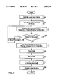
- FIG. 1 shows a flowchart of a method for hierarchical design of a VLSI circuit in accordance with the preferred embodiment of the present invention.
- FIG. 2, FIG. 3 and FIG. 4 are block diagrams which illustrate stages of the determination of placement of circuit logic upon a chip in accordance with the preferred embodiment of the present invention.
- FIG. 1 is a flowchart for the hierarchical design of a VLSI circuit and lay out of the VLSI circuit on a chip.
- a logic level netlist is generated.
- Stephen M. Trimberger An Introduction to CAD for VLSI, Kluwer Academic Publishers, Boston, 1987, pp. 7, 136.
- a step 11 the logic circuitry to be placed is apportioned into component blocks of logical components and an initial floor-plan is developed.
- an estimate is made of the size and shape of each component block.
- the size maybe estimated, for example, by using formulae which generate an estimated size of a component block based on the number of logical components within the component block.
- FIG. 2 The result of an initial floor-plan is shown in FIG. 2.
- a first component block 21, a second component block 22 and a third component block 23 are shown located within a chip 20.
- a step 12 after the initial floor-plan of the component blocks is made, the initial floor-plan is evaluated. During this evaluation additional information about the component blocks is determined and a global route of the major connection networks of the circuit is performed.
- the first step of the evaluation includes, for example, a re-estimate of component block size and shape. This is done, for example, by a quick placement and routing of standard logic cell blocks within the component block.
- a non-optimized placement algorithm such as a minimum cut algorithm may be used for the placement of logical components within the component blocks.
- a non-optimized routing algorithm such as a Steiner tree algorithm may be used for the routing within each component block.
- component block 21 is shown to be a hierarchical component block which has a first logic cell block 31, a second logic cell block 32 and a third logic cell block 33.
- Component block 22 is RAM.
- Component block 23 is composed of standard logic cells. The non-optimized placement and routing of the standard logic cells yields additional information about the component blocks that is used to locate connector areas of the major connection networks to the component blocks and to determine the approximate current which need to be supplied at the connector areas.
- Major connection networks are, for example, connection networks which are used for supplying power, for supplying ground and for supplying a clock signal.
- a non-optimized global route between the component blocks may be performed.
- the global routing connects the major connection networks to the appropriate connector areas.
- This global routing is performed with a non-optimized routing algorithm such as a Steiner Tree algorithm.
- the non-optimized global routing is performed, the locations of input/output pads for the chip may be determined.
- FIG. 4 shows the result of a global routing of the major connection networks.
- a power connection network 51 is shown connected to an input/output pad 41 and various connector locations within component block 21, component block 22 and component block 23.
- a ground connection network 52 is shown connected to an input/output pad 42, and input/output pad 62, an input/output pad 72 and various connector locations within component block 21, component block 22 and component block 23.
- a clock connection network 53 is shown connected to an input/output pad 43 and various connector locations within component block 21, component block 22 and component block 23.
- a step 13 after the global routing of the major connection networks is complete, the floor-plan is evaluated to see if the routing of the major connection networks will make the initial floor-plan unworkable. This can happen, for example, when the space between component blocks is not sufficiently large to accommodate one or more major connection networks routed between them. If necessary, the floor-plan is adjusted in a step 19. The adjusted floor-plan is then re-evaluated in step 12.
- the non-optimized global routing between the component blocks is used to generate routing guidance information for the major connection networks.
- This routing guidance information is essentially a reservation of area on the circuit for placement of the major connection networks. The width of a connection network at a particular location is calculated based on the current required to flow through the connection network at that location. Because the routing guidance information is a reservation of area on the circuit for placement of the major connection networks, the routing guidance may be readily evaluated and modified by a designer at the floor-plan level, before the final layout information is generated.
- a primary advantage of the present invention is the generation of routing guidance information for major connection networks at the floor-plan level.
- prior art systems such as those discussed, for example, by Carl Sechen in Chip-Planning, Placement, and Global Routing of Macro/Custom Cell Integrated Circuits Using Simulated Annealing, 25th ACM/IEEE Design Automation Conference, 1988, pp. 73-80, it is not until after optimized placement and optimized routing of logical circuits within each block has been completed that the floor-plan is evaluated to determine whether the global routing of major connection networks requires adjustments to the floor-plan.
- the global routing of major connection networks is performed before the optimized placement and optimized routing of logical circuits within each component block has been performed.
- the global routing guidance information generated from the global routing of major connection networks designates the routing locations of the major connection networks and thus allows adjustments to be made to the floor-plan at the floor-plan level in order to accommodate the location and size of the major connection networks.
Abstract
Description
Claims (13)
Priority Applications (1)
| Application Number | Priority Date | Filing Date | Title |
|---|---|---|---|
| US07/723,109 US5485396A (en) | 1991-06-28 | 1991-06-28 | Symbolic routing guidance for wire networks in VLSI circuits |
Applications Claiming Priority (1)
| Application Number | Priority Date | Filing Date | Title |
|---|---|---|---|
| US07/723,109 US5485396A (en) | 1991-06-28 | 1991-06-28 | Symbolic routing guidance for wire networks in VLSI circuits |
Publications (1)
| Publication Number | Publication Date |
|---|---|
| US5485396A true US5485396A (en) | 1996-01-16 |
Family
ID=24904886
Family Applications (1)
| Application Number | Title | Priority Date | Filing Date |
|---|---|---|---|
| US07/723,109 Expired - Lifetime US5485396A (en) | 1991-06-28 | 1991-06-28 | Symbolic routing guidance for wire networks in VLSI circuits |
Country Status (1)
| Country | Link |
|---|---|
| US (1) | US5485396A (en) |
Cited By (41)
| Publication number | Priority date | Publication date | Assignee | Title |
|---|---|---|---|---|
| US5638292A (en) * | 1992-01-09 | 1997-06-10 | Kabushiki Kaisha Toshiba | Method for automatically optimizing cell placement |
| US5802075A (en) * | 1997-01-16 | 1998-09-01 | Unisys Corporation | Distributed test pattern generation |
| US5808900A (en) * | 1996-04-30 | 1998-09-15 | Lsi Logic Corporation | Memory having direct strap connection to power supply |
| US5864487A (en) * | 1996-11-19 | 1999-01-26 | Unisys Corporation | Method and apparatus for identifying gated clocks within a circuit design using a standard optimization tool |
| US5870711A (en) * | 1995-12-11 | 1999-02-09 | Sabre Properties, Inc. | Method and system for management of cargo claims |
| US5912820A (en) * | 1997-01-22 | 1999-06-15 | Unisys Corporation | Method and apparatus for distributing a clock tree within a hierarchical circuit design |
| US5956256A (en) * | 1996-11-19 | 1999-09-21 | Unisys Corporation | Method and apparatus for optimizing a circuit design having multi-paths therein |
| US5960184A (en) * | 1996-11-19 | 1999-09-28 | Unisys Corporation | Method and apparatus for providing optimization parameters to a logic optimizer tool |
| US5980092A (en) * | 1996-11-19 | 1999-11-09 | Unisys Corporation | Method and apparatus for optimizing a gated clock structure using a standard optimization tool |
| US6002857A (en) * | 1996-11-14 | 1999-12-14 | Avant! Corporation | Symbolic constraint-based system for preroute reconstruction following floorplan incrementing |
| US6026220A (en) * | 1996-11-19 | 2000-02-15 | Unisys Corporation | Method and apparatus for incremntally optimizing a circuit design |
| US6212668B1 (en) | 1996-05-28 | 2001-04-03 | Altera Corporation | Gain matrix for hierarchical circuit partitioning |
| US6216252B1 (en) * | 1990-04-06 | 2001-04-10 | Lsi Logic Corporation | Method and system for creating, validating, and scaling structural description of electronic device |
| US6230304B1 (en) | 1997-12-24 | 2001-05-08 | Magma Design Automation, Inc. | Method of designing a constraint-driven integrated circuit layout |
| US6249902B1 (en) * | 1998-01-09 | 2001-06-19 | Silicon Perspective Corporation | Design hierarchy-based placement |
| US6301694B1 (en) | 1996-09-25 | 2001-10-09 | Altera Corporation | Hierarchical circuit partitioning using sliding windows |
| US6480997B1 (en) * | 2000-04-04 | 2002-11-12 | Mitsubishi Denki Kabushiki Kaisha | Automatic placement and routing device and method of automatic placement and routing |
| US6487706B1 (en) * | 2000-08-30 | 2002-11-26 | International Business Machines Corporation | Contract methodology for concurrent hierarchical design |
| US6516456B1 (en) | 1997-01-27 | 2003-02-04 | Unisys Corporation | Method and apparatus for selectively viewing nets within a database editor tool |
| US6543040B1 (en) * | 2000-03-15 | 2003-04-01 | International Business Machines Corporation | Macro design techniques to accommodate chip level wiring and circuit placement across the macro |
| US6546532B1 (en) | 2000-06-20 | 2003-04-08 | Unisys Corporation | Method and apparatus for traversing and placing cells using a placement tool |
| US6684376B1 (en) | 1997-01-27 | 2004-01-27 | Unisys Corporation | Method and apparatus for selecting components within a circuit design database |
| US6701289B1 (en) | 1997-01-27 | 2004-03-02 | Unisys Corporation | Method and apparatus for using a placement tool to manipulate cell substitution lists |
| US6708144B1 (en) | 1997-01-27 | 2004-03-16 | Unisys Corporation | Spreadsheet driven I/O buffer synthesis process |
| US6718520B1 (en) | 1997-01-27 | 2004-04-06 | Unisys Corporation | Method and apparatus for selectively providing hierarchy to a circuit design |
| US6754879B1 (en) | 1997-01-27 | 2004-06-22 | Unisys Corporation | Method and apparatus for providing modularity to a behavioral description of a circuit design |
| US20040128638A1 (en) * | 2000-06-20 | 2004-07-01 | Kerzman Joseph Peter | Method and apparatus for selecting and aligning cells using a placement tool |
| US6910200B1 (en) | 1997-01-27 | 2005-06-21 | Unisys Corporation | Method and apparatus for associating selected circuit instances and for performing a group operation thereon |
| US7076410B1 (en) | 1997-01-27 | 2006-07-11 | Unisys Corporation | Method and apparatus for efficiently viewing a number of selected components using a database editor tool |
| US20170357744A1 (en) * | 2016-06-14 | 2017-12-14 | International Business Machines Corporation | Global routing framework of integrated circuit based on localized routing optimization |
| US20180150593A1 (en) * | 2016-11-28 | 2018-05-31 | Fujitsu Limited | Via model generation method, information processing device, and non-transitory computer-readable recording medium storing via model generation program |
| US10719651B2 (en) * | 2017-12-30 | 2020-07-21 | Arteris, Inc. | Synthesizing topology for an interconnect network of a system-on-chip with intellectual property blocks |
| US11558259B2 (en) | 2019-12-27 | 2023-01-17 | Arteris, Inc. | System and method for generating and using physical roadmaps in network synthesis |
| US11601357B2 (en) | 2020-12-22 | 2023-03-07 | Arteris, Inc. | System and method for generation of quality metrics for optimization tasks in topology synthesis of a network |
| US11657203B2 (en) | 2019-12-27 | 2023-05-23 | Arteris, Inc. | Multi-phase topology synthesis of a network-on-chip (NoC) |
| US11665776B2 (en) | 2019-12-27 | 2023-05-30 | Arteris, Inc. | System and method for synthesis of a network-on-chip for deadlock-free transformation |
| US11675942B2 (en) | 2020-12-26 | 2023-06-13 | Arteris, Inc. | Optimization of parameters for synthesis of a topology using a discriminant function module |
| US11748535B2 (en) | 2019-12-27 | 2023-09-05 | Arteris, Inc. | System and method to generate a network-on-chip (NoC) description using incremental topology synthesis |
| US11838211B2 (en) | 2020-04-09 | 2023-12-05 | Arteris, Inc. | System and method to determine optimal path(s) and use load balancing in an interconnect |
| US11836427B2 (en) | 2020-12-30 | 2023-12-05 | Arteris, Inc. | Constraints and objectives used in synthesis of a network-on-chip (NoC) |
| US11956127B2 (en) | 2021-03-10 | 2024-04-09 | Arteris, Inc. | Incremental topology modification of a network-on-chip |
Citations (11)
| Publication number | Priority date | Publication date | Assignee | Title |
|---|---|---|---|---|
| US4580228A (en) * | 1983-06-06 | 1986-04-01 | The United States Of America As Represented By The Secretary Of The Army | Automated design program for LSI and VLSI circuits |
| US4630219A (en) * | 1983-11-23 | 1986-12-16 | International Business Machines Corporation | Element placement method |
| US4918614A (en) * | 1987-06-02 | 1990-04-17 | Lsi Logic Corporation | Hierarchical floorplanner |
| US4964057A (en) * | 1986-11-10 | 1990-10-16 | Nec Corporation | Block placement method |
| US5065355A (en) * | 1988-05-13 | 1991-11-12 | Hitachi, Ltd. | Automatic routing method for LSI |
| US5144563A (en) * | 1989-03-16 | 1992-09-01 | Hitachi, Ltd. | Method and apparatus for optimizing element placement and method and apparatus for deciding the optimal element placement |
| US5187668A (en) * | 1989-12-04 | 1993-02-16 | Matsushita Electric Industrial Co., Ltd. | Placement optimization system aided by cad |
| US5187864A (en) * | 1991-07-26 | 1993-02-23 | Vlsi Technology, Inc. | Adaptable topologies used in routing of ground and power networks on integrated circuits |
| US5191542A (en) * | 1989-06-23 | 1993-03-02 | Kabushiki Kaisha Toshiba | Automatic floorplan operation apparatus |
| US5208759A (en) * | 1990-12-13 | 1993-05-04 | Vlsi Technology, Inc. | Method for placement of circuit components in an integrated circuit |
| US5359538A (en) * | 1991-08-20 | 1994-10-25 | Vlsi Technology, Inc. | Method for regular placement of data path components in VLSI circuits |
-
1991
- 1991-06-28 US US07/723,109 patent/US5485396A/en not_active Expired - Lifetime
Patent Citations (11)
| Publication number | Priority date | Publication date | Assignee | Title |
|---|---|---|---|---|
| US4580228A (en) * | 1983-06-06 | 1986-04-01 | The United States Of America As Represented By The Secretary Of The Army | Automated design program for LSI and VLSI circuits |
| US4630219A (en) * | 1983-11-23 | 1986-12-16 | International Business Machines Corporation | Element placement method |
| US4964057A (en) * | 1986-11-10 | 1990-10-16 | Nec Corporation | Block placement method |
| US4918614A (en) * | 1987-06-02 | 1990-04-17 | Lsi Logic Corporation | Hierarchical floorplanner |
| US5065355A (en) * | 1988-05-13 | 1991-11-12 | Hitachi, Ltd. | Automatic routing method for LSI |
| US5144563A (en) * | 1989-03-16 | 1992-09-01 | Hitachi, Ltd. | Method and apparatus for optimizing element placement and method and apparatus for deciding the optimal element placement |
| US5191542A (en) * | 1989-06-23 | 1993-03-02 | Kabushiki Kaisha Toshiba | Automatic floorplan operation apparatus |
| US5187668A (en) * | 1989-12-04 | 1993-02-16 | Matsushita Electric Industrial Co., Ltd. | Placement optimization system aided by cad |
| US5208759A (en) * | 1990-12-13 | 1993-05-04 | Vlsi Technology, Inc. | Method for placement of circuit components in an integrated circuit |
| US5187864A (en) * | 1991-07-26 | 1993-02-23 | Vlsi Technology, Inc. | Adaptable topologies used in routing of ground and power networks on integrated circuits |
| US5359538A (en) * | 1991-08-20 | 1994-10-25 | Vlsi Technology, Inc. | Method for regular placement of data path components in VLSI circuits |
Non-Patent Citations (24)
| Title |
|---|
| "A Block Interconnection Algorithm for Hierarchical Layout System" by Fukui et al., IEEE Trans. on Computer-Aided Design, vol. CAD-6, No. 3, May 1987, pp. 383-390. |
| "A New Area-Efficient Power Routing Algorithm for VLSI Layout" by Haryama et al., IEEE 1987, pp. 38-41. |
| "An Antomatic Routing System for General Cell VLSI Circuits" by Dai et al., IEEE 1985 Custom Integrated Circuits Conf., 1985, pp. 68-71. |
| "Automatic Placement-A Review of Current Techniques" by Preas et al., IEEE 23rd Design Automation Cont., 1986, pp. 622-629. |
| "Computation of Power Supply Nets in VLSI Layout" by Rothermel et al., IEEE 18th Design Automation Conference, 1981, pp. 37-42. |
| "Philo-A VLSI Design System" by Donze et al., IEEE 19th Design Automation Conf., 1982, pp. 163-169. |
| "Single Layer Routing of Power and Ground Networks in Integrated Circuits" by Syed et al., Journal of Digital Systems, vol. VI, No. 1, pp. 53-63, 1987. |
| "The Scan Line Approach To Power and Ground Routing" by Xiong et al., IEEE 1986, pp. 6-9. |
| A Block Interconnection Algorithm for Hierarchical Layout System by Fukui et al., IEEE Trans. on Computer Aided Design, vol. CAD 6, No. 3, May 1987, pp. 383 390. * |
| A New Area Efficient Power Routing Algorithm for VLSI Layout by Haryama et al., IEEE 1987, pp. 38 41. * |
| An Antomatic Routing System for General Cell VLSI Circuits by Dai et al., IEEE 1985 Custom Integrated Circuits Conf., 1985, pp. 68 71. * |
| Andrew S. Moulton, Laying the Power and Ground Wires on a VLSI Chip, 20th Design Automation conference, IEEE, 1983, pp. 754 755. * |
| Andrew S. Moulton, Laying the Power and Ground Wires on a VLSI Chip, 20th Design Automation conference, IEEE, 1983, pp. 754-755. |
| Automatic Placement A Review of Current Techniques by Preas et al., IEEE 23rd Design Automation Cont., 1986, pp. 622 629. * |
| B. W. Kernighan and S. Lin; An Efficient Heuristic Procedure for Partitioning Graphs, Bell System Technical Journal; 49(2):291 307; Feb. 1970. * |
| B. W. Kernighan and S. Lin; An Efficient Heuristic Procedure for Partitioning Graphs, Bell System Technical Journal; 49(2):291-307; Feb. 1970. |
| Computation of Power Supply Nets in VLSI Layout by Rothermel et al., IEEE 18th Design Automation Conference, 1981, pp. 37 42. * |
| David W. Russell, Hierarchical Routing of Single Layer Metal Trees in Compiled VLSI, ICCAD, IEEE, 1985, pp. 270 272. * |
| David W. Russell, Hierarchical Routing of Single Layer Metal Trees in Compiled VLSI, ICCAD, IEEE, 1985, pp. 270-272. |
| H. Cho, G. Hachtel, M. Nach, and L. Setiono; Beat NP: A tool for Partitioning Boolean Networks; Proceedings of the ICCAD, pp. 10 13; Nov. 1988. * |
| H. Cho, G. Hachtel, M. Nach, and L. Setiono; Beat NP: A tool for Partitioning Boolean Networks; Proceedings of the ICCAD, pp. 10-13; Nov. 1988. |
| Philo A VLSI Design System by Donze et al., IEEE 19th Design Automation Conf., 1982, pp. 163 169. * |
| Single Layer Routing of Power and Ground Networks in Integrated Circuits by Syed et al., Journal of Digital Systems, vol. VI, No. 1, pp. 53 63, 1987. * |
| The Scan Line Approach To Power and Ground Routing by Xiong et al., IEEE 1986, pp. 6 9. * |
Cited By (48)
| Publication number | Priority date | Publication date | Assignee | Title |
|---|---|---|---|---|
| US6216252B1 (en) * | 1990-04-06 | 2001-04-10 | Lsi Logic Corporation | Method and system for creating, validating, and scaling structural description of electronic device |
| US5638292A (en) * | 1992-01-09 | 1997-06-10 | Kabushiki Kaisha Toshiba | Method for automatically optimizing cell placement |
| US5870711A (en) * | 1995-12-11 | 1999-02-09 | Sabre Properties, Inc. | Method and system for management of cargo claims |
| US5808900A (en) * | 1996-04-30 | 1998-09-15 | Lsi Logic Corporation | Memory having direct strap connection to power supply |
| US6212668B1 (en) | 1996-05-28 | 2001-04-03 | Altera Corporation | Gain matrix for hierarchical circuit partitioning |
| US6301694B1 (en) | 1996-09-25 | 2001-10-09 | Altera Corporation | Hierarchical circuit partitioning using sliding windows |
| US6002857A (en) * | 1996-11-14 | 1999-12-14 | Avant! Corporation | Symbolic constraint-based system for preroute reconstruction following floorplan incrementing |
| US5864487A (en) * | 1996-11-19 | 1999-01-26 | Unisys Corporation | Method and apparatus for identifying gated clocks within a circuit design using a standard optimization tool |
| US5980092A (en) * | 1996-11-19 | 1999-11-09 | Unisys Corporation | Method and apparatus for optimizing a gated clock structure using a standard optimization tool |
| US5960184A (en) * | 1996-11-19 | 1999-09-28 | Unisys Corporation | Method and apparatus for providing optimization parameters to a logic optimizer tool |
| US6026220A (en) * | 1996-11-19 | 2000-02-15 | Unisys Corporation | Method and apparatus for incremntally optimizing a circuit design |
| US5956256A (en) * | 1996-11-19 | 1999-09-21 | Unisys Corporation | Method and apparatus for optimizing a circuit design having multi-paths therein |
| US5802075A (en) * | 1997-01-16 | 1998-09-01 | Unisys Corporation | Distributed test pattern generation |
| US5912820A (en) * | 1997-01-22 | 1999-06-15 | Unisys Corporation | Method and apparatus for distributing a clock tree within a hierarchical circuit design |
| US6708144B1 (en) | 1997-01-27 | 2004-03-16 | Unisys Corporation | Spreadsheet driven I/O buffer synthesis process |
| US6910200B1 (en) | 1997-01-27 | 2005-06-21 | Unisys Corporation | Method and apparatus for associating selected circuit instances and for performing a group operation thereon |
| US7076410B1 (en) | 1997-01-27 | 2006-07-11 | Unisys Corporation | Method and apparatus for efficiently viewing a number of selected components using a database editor tool |
| US6754879B1 (en) | 1997-01-27 | 2004-06-22 | Unisys Corporation | Method and apparatus for providing modularity to a behavioral description of a circuit design |
| US6516456B1 (en) | 1997-01-27 | 2003-02-04 | Unisys Corporation | Method and apparatus for selectively viewing nets within a database editor tool |
| US6718520B1 (en) | 1997-01-27 | 2004-04-06 | Unisys Corporation | Method and apparatus for selectively providing hierarchy to a circuit design |
| US6701289B1 (en) | 1997-01-27 | 2004-03-02 | Unisys Corporation | Method and apparatus for using a placement tool to manipulate cell substitution lists |
| US6684376B1 (en) | 1997-01-27 | 2004-01-27 | Unisys Corporation | Method and apparatus for selecting components within a circuit design database |
| US6230304B1 (en) | 1997-12-24 | 2001-05-08 | Magma Design Automation, Inc. | Method of designing a constraint-driven integrated circuit layout |
| US6249902B1 (en) * | 1998-01-09 | 2001-06-19 | Silicon Perspective Corporation | Design hierarchy-based placement |
| US20030204829A1 (en) * | 2000-03-15 | 2003-10-30 | International Business Machines Corporation | Macro design techniques to accommodate chip level wiring and circuit placement across the macro |
| US6543040B1 (en) * | 2000-03-15 | 2003-04-01 | International Business Machines Corporation | Macro design techniques to accommodate chip level wiring and circuit placement across the macro |
| US20050039153A1 (en) * | 2000-03-15 | 2005-02-17 | International Business Machines Corporation | Macro design techniques to accommodate chip level wiring and circuit placement across the macro |
| US6883155B2 (en) * | 2000-03-15 | 2005-04-19 | International Business Machines Corporation | Macro design techniques to accommodate chip level wiring and circuit placement across the macro |
| US7096436B2 (en) | 2000-03-15 | 2006-08-22 | International Business Machines Corporation | Macro design techniques to accommodate chip level wiring and circuit placement across the macro |
| US6480997B1 (en) * | 2000-04-04 | 2002-11-12 | Mitsubishi Denki Kabushiki Kaisha | Automatic placement and routing device and method of automatic placement and routing |
| US6546532B1 (en) | 2000-06-20 | 2003-04-08 | Unisys Corporation | Method and apparatus for traversing and placing cells using a placement tool |
| US20040128638A1 (en) * | 2000-06-20 | 2004-07-01 | Kerzman Joseph Peter | Method and apparatus for selecting and aligning cells using a placement tool |
| US6889370B1 (en) | 2000-06-20 | 2005-05-03 | Unisys Corporation | Method and apparatus for selecting and aligning cells using a placement tool |
| US6487706B1 (en) * | 2000-08-30 | 2002-11-26 | International Business Machines Corporation | Contract methodology for concurrent hierarchical design |
| US20170357744A1 (en) * | 2016-06-14 | 2017-12-14 | International Business Machines Corporation | Global routing framework of integrated circuit based on localized routing optimization |
| US10120970B2 (en) * | 2016-06-14 | 2018-11-06 | International Business Machines Corporation | Global routing framework of integrated circuit based on localized routing optimization |
| US20180150593A1 (en) * | 2016-11-28 | 2018-05-31 | Fujitsu Limited | Via model generation method, information processing device, and non-transitory computer-readable recording medium storing via model generation program |
| US10719651B2 (en) * | 2017-12-30 | 2020-07-21 | Arteris, Inc. | Synthesizing topology for an interconnect network of a system-on-chip with intellectual property blocks |
| US11665776B2 (en) | 2019-12-27 | 2023-05-30 | Arteris, Inc. | System and method for synthesis of a network-on-chip for deadlock-free transformation |
| US11657203B2 (en) | 2019-12-27 | 2023-05-23 | Arteris, Inc. | Multi-phase topology synthesis of a network-on-chip (NoC) |
| US11558259B2 (en) | 2019-12-27 | 2023-01-17 | Arteris, Inc. | System and method for generating and using physical roadmaps in network synthesis |
| US11748535B2 (en) | 2019-12-27 | 2023-09-05 | Arteris, Inc. | System and method to generate a network-on-chip (NoC) description using incremental topology synthesis |
| US11838211B2 (en) | 2020-04-09 | 2023-12-05 | Arteris, Inc. | System and method to determine optimal path(s) and use load balancing in an interconnect |
| US11601357B2 (en) | 2020-12-22 | 2023-03-07 | Arteris, Inc. | System and method for generation of quality metrics for optimization tasks in topology synthesis of a network |
| US11784909B2 (en) | 2020-12-22 | 2023-10-10 | Arteris, Inc. | Quality metrics for optimization tasks in generation of a network |
| US11675942B2 (en) | 2020-12-26 | 2023-06-13 | Arteris, Inc. | Optimization of parameters for synthesis of a topology using a discriminant function module |
| US11836427B2 (en) | 2020-12-30 | 2023-12-05 | Arteris, Inc. | Constraints and objectives used in synthesis of a network-on-chip (NoC) |
| US11956127B2 (en) | 2021-03-10 | 2024-04-09 | Arteris, Inc. | Incremental topology modification of a network-on-chip |
Similar Documents
| Publication | Publication Date | Title |
|---|---|---|
| US5485396A (en) | Symbolic routing guidance for wire networks in VLSI circuits | |
| US6415422B1 (en) | Method and system for performing capacitance estimations on an integrated circuit design routed by a global routing tool | |
| US5349542A (en) | Method for sizing widths of power busses in integrated circuits | |
| US6543043B1 (en) | Inter-region constraint-based router for use in electronic design automation | |
| US5623420A (en) | Method and apparatus to distribute spare cells within a standard cell region of an integrated circuit | |
| US6002857A (en) | Symbolic constraint-based system for preroute reconstruction following floorplan incrementing | |
| US7228514B2 (en) | Method, system and computer program product for automatically estimating pin locations and interconnect parasitics of a circuit layout | |
| US6009248A (en) | Delay optimization system to conduct optimization for satisfying delay constraints on the circuit and method therefor | |
| US7346869B2 (en) | Power network analyzer for an integrated circuit design | |
| US6553338B1 (en) | Timing optimization in presence of interconnect delays | |
| US20030233628A1 (en) | Technology dependent transformations in CMOS and silicon-on-insulator during digital design synthesis | |
| US20030079192A1 (en) | Method for generating a partitioned ic layout | |
| US20090178013A1 (en) | System for implementing post-silicon ic design changes | |
| US7360190B1 (en) | Method and apparatus for performing retiming on field programmable gate arrays | |
| Poirier | Excellerator: Custom CMOS leaf cell layout generator | |
| US6684373B1 (en) | Optimize global net timing with repeater buffers | |
| Xu et al. | Layout-driven RTL binding techniques for high-level synthesis using accurate estimators | |
| US5978572A (en) | LSI wire length estimation and area estimation | |
| US7257800B1 (en) | Method and apparatus for performing logic replication in field programmable gate arrays | |
| Cong et al. | Buffer block planning for interconnect planning and prediction | |
| Balachandran et al. | A-priori wirelength and interconnect estimation based on circuit characteristics | |
| US6941532B2 (en) | Clock skew verification methodology for grid-based design | |
| CN101369294A (en) | Plane layout planning method for SoC layout | |
| US6557144B1 (en) | Netlist resynthesis program based on physical delay calculation | |
| Manohararajah et al. | Predicting interconnect delay for physical synthesis in a FPGA CAD flow |
Legal Events
| Date | Code | Title | Description |
|---|---|---|---|
| AS | Assignment |
Owner name: VLSI TECHNOLOGY, INC. A CORP. OF DELAWARE, CALIF Free format text: ASSIGNMENT OF ASSIGNORS INTEREST.;ASSIGNORS:BRASEN, DANIEL R.;ASHTAPUTRE, SUNIL;REEL/FRAME:005762/0480 Effective date: 19910626 |
|
| FPAY | Fee payment |
Year of fee payment: 4 |
|
| FEPP | Fee payment procedure |
Free format text: PAYOR NUMBER ASSIGNED (ORIGINAL EVENT CODE: ASPN); ENTITY STATUS OF PATENT OWNER: LARGE ENTITY |
|
| FPAY | Fee payment |
Year of fee payment: 8 |
|
| REMI | Maintenance fee reminder mailed | ||
| FEPP | Fee payment procedure |
Free format text: PETITION RELATED TO MAINTENANCE FEES GRANTED (ORIGINAL EVENT CODE: PMFG); ENTITY STATUS OF PATENT OWNER: LARGE ENTITY Free format text: PETITION RELATED TO MAINTENANCE FEES FILED (ORIGINAL EVENT CODE: PMFP); ENTITY STATUS OF PATENT OWNER: LARGE ENTITY |
|
| REIN | Reinstatement after maintenance fee payment confirmed | ||
| FP | Lapsed due to failure to pay maintenance fee |
Effective date: 20080116 |
|
| PRDP | Patent reinstated due to the acceptance of a late maintenance fee |
Effective date: 20081217 |
|
| FPAY | Fee payment |
Year of fee payment: 12 |
|
| STCF | Information on status: patent grant |
Free format text: PATENTED CASE |
|
| SULP | Surcharge for late payment | ||
| AS | Assignment |
Owner name: NXP B.V., NETHERLANDS Free format text: ASSIGNMENT OF ASSIGNORS INTEREST;ASSIGNOR:PHILIPS SEMICONDUCTORS INC.;REEL/FRAME:022973/0239 Effective date: 20090715 Owner name: PHILIPS SEMICONDUCTORS VLSI INC., NEW YORK Free format text: CHANGE OF NAME;ASSIGNOR:VLSI TECHNOLOGY, INC.;REEL/FRAME:022973/0248 Effective date: 19990702 Owner name: PHILIPS SEMICONDUCTORS INC., NEW YORK Free format text: CHANGE OF NAME;ASSIGNOR:PHILIPS SEMICONDUCTORS VLSI INC.;REEL/FRAME:022973/0254 Effective date: 19991229 |