US5491729A - Digital phase-locked data recovery circuit - Google Patents
Digital phase-locked data recovery circuit Download PDFInfo
- Publication number
- US5491729A US5491729A US08/337,965 US33796594A US5491729A US 5491729 A US5491729 A US 5491729A US 33796594 A US33796594 A US 33796594A US 5491729 A US5491729 A US 5491729A
- Authority
- US
- United States
- Prior art keywords
- phase
- clock
- signals
- boundary
- samples
- Prior art date
- Legal status (The legal status is an assumption and is not a legal conclusion. Google has not performed a legal analysis and makes no representation as to the accuracy of the status listed.)
- Expired - Lifetime
Links
Images


Classifications
-
- H—ELECTRICITY
- H04—ELECTRIC COMMUNICATION TECHNIQUE
- H04L—TRANSMISSION OF DIGITAL INFORMATION, e.g. TELEGRAPHIC COMMUNICATION
- H04L7/00—Arrangements for synchronising receiver with transmitter
- H04L7/02—Speed or phase control by the received code signals, the signals containing no special synchronisation information
- H04L7/033—Speed or phase control by the received code signals, the signals containing no special synchronisation information using the transitions of the received signal to control the phase of the synchronising-signal-generating means, e.g. using a phase-locked loop
- H04L7/0337—Selecting between two or more discretely delayed clocks or selecting between two or more discretely delayed received code signals
Definitions
- the present invention relates to the recovery of clock timing information from data transmitted within digital systems. More specifically, this invention relates to phase-locked methods of synchronizing the phase of a locally-generated receiver clock with that of the transmitted waveform.
- Local area networks facilitate economical data communication between computing systems clustered in a locality.
- Examples of such networks used widely in the art include token ring LAN's and Ethernet LAN's.
- a token ring LAN is a circular network having a plurality of stations (nodes) interconnected in a ring topology. Access to the network is controlled by the possession of a signal "token".
- the token is a packet of signals that is passed from node to node.
- the node that has the token has control of the network with respect to the transmission of data to other nodes and the receipt of data from the same. When the node has completed a transmission, the token is released for acquisition by another node.
- Errors in data transmission within the ring can generally be minimized by operating the ring in a synchronous mode. That is, in order to decode a baseband data waveform a clock signal giving the proper sampling time must be available. Pilot tones are sometimes transmitted along with the data waveform for this purpose. Alternatively, timing may be derived directly from the data waveform itself.
- One approach to such "self-timing" involves allowing the data to pass through a memoryless nonlinearity and then ring a tuned circuit with a resonant frequency close to the nominal data (bit) rate. Nonetheless, this approach is relatively imprecise in comparison with those which utilize phase-locked loops (PLL's).
- a Manchester encoded waveform may be synthesized by combining a binary data pattern with a transmitter clock operative at twice the transmitted bit frequency.
- a transition corresponding to a transmitter clock signal occurs at every midbit interval of a Manchester data bit irrespective of the specific data pattern.
- Clock synchronization within a receiver is initially effected by transmitting a preamble consisting of a Manchester encoded waveform having no steps at bit boundaries. This allows individually received data bits to be distinguished, thus obviating the need for a separately transmitted clock signal.
- the receiver decodes the Manchester data by sampling each received data bit at several time intervals.
- the receiver clock must remain sufficiently matched to the transmitter clock or samples may be taken on the "wrong" side of the midbit transition. For example, if sampling is to occur within one-fourth bit of the transmitted clock edges the receiver clock must be matched within twenty-five percent of the transmitted clock. Otherwise, samples will be taken from outside the bit boundaries or on the wrong side of the mid-bit steps.
- the phase of the receiver clock must be matched to within 25 nanoseconds of the phase of the transmitter clock in order to ensure accurate decoding.
- a conventional PLL receiver network remains in timing synchronization by adjusting its clock phase relative to transitions within the transmitted data.
- the transmitted and recovered clock signals are provided to a comparator.
- the comparator produces an error voltage in response to a phase difference between the clock signals.
- the error voltage is then filtered and applied to a voltage controlled oscillator (VCO) for synthesizing the recovered clock waveform.
- VCO voltage controlled oscillator
- analog PLL's offer potentially high resolution
- the need for precision circuit components may unacceptably increase costs.
- the susceptibility of analog circuits to signal noise tends to limit the resolution effectively obtained in practical applications.
- Digital PLL circuits do not require precision circuit elements. Nonetheless, the resolution of a digital PLL is constrained by the number of samples which may be taken during each bit period.
- Digital PLL's typically employ a counter which is incremented during each cycle of the recovered clock. Upon reaching a predetermined value, the counter issues a sample clock pulse to be compared with the received clock signals. In general, if the sample pulses lead the received clock a pulse is deleted from the pulse stream feeding the counter in order to delay the count. Alternatively, the limit of the counter may be incremented by one in order to obviate the need to delete a pulse as a means of delaying issuance of the next sample pulse. Similarly, if the sample clock signals lag the received clock an additional pulse is supplied by a driver clock to the counter pulse stream.
- this operational mode requires that the pulse stream provided to the counter be modified at a relatively high rate. For example, in order to extract 32 bits per sample from a 10 Mbps data signal the driver clock would need to operate at approximately 320 MHz. Because of the difficulty in generating a sampling clock signal of 320 MHz, digital PLL decoding techniques using a single driver clock are of limited utility in high frequency applications.
- At least one technique has been proposed which purports to overcome the constraints on sampling intervals imposed by the requirement of a high frequency clock driver.
- a multi-phase driver clock provides clock signals phase-offset from each other.
- One clock output signal is used as the driver clock to clock an input sampler.
- a pattern of bit samples before, nominally at, and after a predicted clock edge indicates whether a leading or lagging phase should be substituted for the present driver clock signal.
- the multiphase technique disclosed by Wong, et al. does not furnish information regarding the magnitude of the lead/lag error.
- the absence of such information may introduce, for example, jitter in the recovered clock signal.
- multi-phase techniques disposed to reflexively add or subtract from the counter pulse stream tend to unnecessarily introduce jitter into the recovered clock waveform. That is, corrections are made for transient phase deviations induced by spurious noise as well as for "true" drift of the recovered clock.
- conventional multi-phase sampling methods may be susceptible to signal noise.
- the encoded waveform is generally sampled uniformly throughout each bit period.
- Manchester waveforms there is the possibility that a transition at a bit boundary will be mistaken for a midbit transition resulting from a noise-induced phase shift of the data signal.
- the inventive data recovery circuit includes a multi-phase clock for supplying clock signals having a predetermined relative phase relationship.
- a snap shot sampling network takes samples of an input data signal in response to the multi-phase clock signals. The samples are collected during boundary sampling windows encompassing transitions in the input data signal.
- the invention further includes a network for comparing the received data samples with a sample pattern.
- a phase encoder then generates error signals in response to the phase comparisons.
- a phase decoder adjusts the phase of the boundary window in response to the error signal.
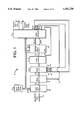
- FIG. 1 is a block diagram of a preferred embodiment of the digital phase-locked data recovery circuit of the present invention
- FIG. 2 shows the relative phase relationship of the eight clock phases 40, 41, 42, 43, 44, 45, 46, and 47 provided by a multi-phase clock.
- FIG. 3 shows a schematic representation of a snapshot sampler included within the inventive data recovery circuit.
- FIG. 4 is an illustrative block diagram of a phase rotator operatively connected to the snap shot sampler.
- FIG. 5 shows a schematic representation of a first multiplexer module included within the phase rotator.
- FIG. 6 shows a schematic representation of a phase latch network disposed to collect sets of sample data from the phase rotator.
- FIG. 7 is a timing diagram depicting the manner in which Manchester data impressed on an input line is latched by a set of flip-flops included within the phase latch.
- FIGS. 8a and 8b together yield a schematic representation of a phase encoder network operative to provide a stream of phase error signals.
- FIG. 9 is a block diagram of a programmable filter addressed by the phase encoder network.
- FIGS. 10a, 10b and 10c show a schematic representation of a phase decoder included within the inventive data recovery circuit.
- FIG. 1 is a block diagram of a preferred embodiment of the digital phase-locked data recovery circuit 10 of the present invention.
- the inventive circuit 10 receives Manchester encoded data at an input line 12, and operates to recover therefrom clock and data waveforms at output terminals 16 and 18.
- a multi-phase clock 22 provides a set of clock signals equally spaced in phase upon a set of clock driver lines 26.
- the multi-phase clock 22 generates eight 40 MHz clock signals frequency-locked to a 20 MHz crystal oscillator (not shown). More specifically, FIG. 2 shows the uniform relative phase relationship of the eight clock phases ⁇ 0 , ⁇ 1 , ⁇ 2 , ⁇ 3 , ⁇ 4 , ⁇ 5 , ⁇ 6 , ⁇ 7 .
- the clock 22 may be realized as described in copending U.S. patent application Ser. No.
- FIG. 3 shows a schematic representation of the snap-shot sampler 32.
- the clock phases ⁇ 0 , ⁇ 1 , ⁇ 2 , ⁇ 3 , ⁇ 4 , ⁇ 5 , ⁇ 6 , ⁇ 7 each drive the clock (CK) input of identical D-type flip-flops 40.
- the Manchester data is supplied to each of the flip-flops 40 via the input line 12.
- the Q outputs of the flip-flops 40 provide eight data samples S0, S1, S2, S3, S4, S5, S6 and S7 during each complete cycle through the phases of the clock generator 22.
- the data samples S0, S1, S2, S3, S4, S5, S6 and S7, stored by the snap-shot sampler 32, are transmitted to a phase rotator 44 over a set of eight sampler output lines 48.
- FIG. 4 is an illustrative block diagram of the phase rotator 44.
- the phase rotator 44 includes eight identical phase multiplexer modules 52, each of which are addressed by the sampler output lines 48.
- Each multiplexer module 52 is separately actuated by first, second, third, fourth, fifth, sixth, seventh and eighth separate boundary select driver lines 56, 58, 60, 62, 64, 66, 68 and 70.
- boundary select driver lines are shown as being incorporated within a boundary select driver bus 72 in communication with a phase decoder 74 (FIG. 1).
- FIG. 5 shows a schematic representation of the first multiplexer module 52, it being understood that the remaining multiplexer modules are substantially identical thereto.
- the module 52 includes eight transmission gates 80, each of which are addressed by the first boundary select line 56. Upon being enabled by the select line 56, each of the gates 80 passes one of the data samples S0, S1, S2, S3, S4, S5, S6 and S7, thereby creating a set of eight rotated data samples SR0, SR1, SR2, SR3, SR4, SR5, SR6 and SR7.
- the rotated data samples SR0, SR1, SR2, SR3, SR4, SR5, SR6 and SR7 are forwarded by the gates 80 to eight separate signal lines (not individually shown) included within a phase rotator bus 84.
- the bus 4 is similarly coupled to the eight transmission gates within each of the multiplexer modules. Data rotation is simply performed by enabling the appropriate boundary select line 56, 58, 60, 62, 64, 66, 68 or 70. Only a single boundary select line is enabled at any given time.
- the first multiplexer 52 maps the data samples S0, S1, S2, S3, S4, S5, S6 and S7 to rotated data samples SR0, SR1, SR2, SR3, SR4, SR5, SR6 and SR7.
- the second multiplexer 52 maps the data samples S1, S2, S3, S4, S5, S6, S7 and SO to rotated data samples SR0, SR1, SR2, SR3, SR4, SR5, SR6 and SR7.
- phase rotator bus 84 conducts the rotated data samples to a phase latch 88.
- the phase latch 88 is also addressed by first, second, third and fourth latch enable lines from the phase decoder 74.
- FIG. 6 shows a schematic representation of the phase latch 88.
- the first, second, third and fourth latch enable lines 92, 94, 96 and 98 are used to clock first, second, third and fourth sets 102, 104, 106 and 108 of D-type latch flip-flops, respectively.
- the rotated data samples SR0, SR1, SR2 and SR3 are supplied to the first and third sets of flip-flops 102 and 106.
- the rotated samples SR4, SR5, SR6 and SR7 are routed to the second and fourth sets of latch flip-flops 104 and 108.
- FIG. 6 shows a schematic representation of the phase latch 88.
- the first, second, third and fourth latch enable lines 92, 94, 96 and 98 are used to clock first, second, third and fourth sets 102, 104, 106 and 108 of D-type latch flip-flops, respectively.
- the rotated data samples SR0, SR1, SR2 and SR3 are supplied to
- reference symbols A0, A1, A2, A3, A4, A5, A6 and A7 serve to identify the Q output terminals of the first and second sets of latch flip-flops 102 and 104.
- reference symbols B0, B1, B2, B3, B4, B5, B6 and B7 are employed to label the Q output terminals of the third and fourth sets of latch flip flops 106 and 108.
- FIG. 7 is a timing diagram depicting the manner in which Manchester data impressed on the input line 12 is latched by the flip-flops included within the phase latch 88.
- FIG. 7 shows the interlaced transitions of the 40 MHz clock phases ⁇ 0 , ⁇ 1 , ⁇ 2 , ⁇ 3 , ⁇ 4 , ⁇ 5 , ⁇ 6 , and ⁇ 7 relative to 40 MHz, 20 MHz and 10 MHz square waves in synchrony with the clock phase ⁇ 0 .
- the inventive circuit 10 operates to sample the input Manchester waveform within boundary sampling windows confined to the vicinity surrounding each midbit data transition.
- the boundary window surrounding each midbit transition is defined by two periods of one of the eight clock phases ⁇ 0 , ⁇ 1 , ⁇ 2 , ⁇ 3 , ⁇ 4 , ⁇ 5 , ⁇ 6 , and ⁇ 7 , and in the particular example of FIG. 7 is defined by the logically high portion of a 90 degree phase-shifted (quadrature) version of the 10 MHz square wave denoted by V10Q.
- the particular clock phase selected to define the boundary window is that which includes a rising transition most closely aligned with the Manchester midbit transition. For example, in FIG.
- the transitions in clock phase ⁇ 5 at times t B1 and t B2 define a 50 nanosecond boundary window W centered approximately about the midbit Manchester transition occurring at time t M .
- a boundary window nominally remains centered over each midbit transition in the 10 Mbps Manchester waveform.
- the waveform defined by shifting the boundary window by one-quarter period corresponds to a recovered clock signal phase-locked with the input Manchester data.
- Boundary select line 72 determines at which particular clock transition within the boundary window that data will initially be read. Data samples are then accumulated by the sampler 32 synchronously with rising transitions in the sequential clock phases which follow the clock transition during which data is initially read. Again, since the boundary window W commences with clock phase ⁇ 5 the sixth boundary select line 66 is raised during transmission of the collected samples from the sampler 32 to the phase rotator 44. In this manner, the first sample accumulated by the sampler 32 is transformed into rotated data sample SR0 within the phase rotator 44, the second collected sample corresponds to the rotated sample SR1, and so on. The phase rotator 44 thus operates to order (i.e. rotate) the data samples S0, S1, S2, S3, S4, S5, S6 and S7 within the boundary window W. Again, the sequential arrangement of the data samples within the window W is determined by the particular boundary select driver line pulsed by the phase decoder 74.
- the first latch enable line 92 is raised by the phase decoder 74 in order to cause the first four rotated samples SR0, SR1, SR2 and SR3 to be latched by the first set of flip-flops 102 within the phase latch 88.
- the first latch enable line 92 is lowered and the second latch enable line 94 is raised in order to latch the rotated samples SR4, SR5, SR6 and SR7 within the second set of phase latch flip-flops 104.
- the second set of four accumulated data samples replace the first four accumulated samples within the multiplexer module 52.
- the third latch enable line 96 is raised by the phase decoder 74 in order to cause the first four rotated samples SR0, SR1, SR2 and SR3 to be latched by the third set of phase latch flip-flops 106.
- the third latch enable line 96 is then lowered and the fourth latch enable line 98 is contemporaneously raised.
- the rotated samples SR4, SR5, SR6 and SR7 of the are latched within the second set of phase latch flip-flops 104. This process continues until a total of sixteen data samples are stored in the phase latch 88.
- the phase latch 88 is operatively connected to a phase encoder 110.
- FIGS. 8a and 8b together depict the Boolean operations performed within the phase encoder 110.
- the phase encoder 110 includes a first Boolean network 110a driven by the Q output terminals of the latch identified by the indicated reference symbols (e.g. A0, A1, B0, B1) latch 88.
- the phase encoder 110 is disposed to estimate the phase differential between the midbit transition of the data signal and the corresponding transition within the recovered clock (FIG. 7).
- the logical output of the first Boolean network 110a maps the midbit data transition to any one of sixteen (i.e., PH0, PH1, . . . PH15) locations within the current boundary window.
- the latch 88 and phase encoder 110 are configured such that three consecutive data samples within the boundary window W forming the patterns "011" or "100” will cause one of the outputs of the network 110a to register a logical high.
- the outputs of the network 110a denoted by reference symbols PH0, PH1, PH2 PH3, PH4, PH5, PH6, PH7, PH8, PH9, PH10, PH11, PH12, PH13, PH14 and PH15 are indicative of the phase of the midbit transition relative to the boundary window W.
- the phase encoder 110 includes a second Boolean network 110b for generating an error signal based on the logical status of the outputs PH0 through PH15 from the first Boolean network 110a.
- the second Boolean network 110b is operative to generate a 4-bit two's complement representation (B3,B2,B1,B0) of the phase information inherent in the signals PH0 through PH15.
- the two's complement error signal is transmitted to a programmable filter 140 over a set of filter driver lines generally indicated by reference numeral 144.
- FIG. 9a shows a block diagrammatic representation of a programmable filter 140.
- the filter 140 includes a programmable gain module 148 addressed by the two's complement error signal (B3, B2, B1, B0).
- the gain module 148 is designed to transform the two's complement error signal to a scaled error signal B' by performing a bit shift operation in accordance with a two-bit digital gain control word (K1, K0).
- Table 1 is a truth table representing the logical operations performed within the gain module 148.
- the truth table may be implemented in a straightforward manner by using, for example, an appropriate arrangement of transmission gates. By appropriately scaling the two's complement error signal the loop gain of the circuit 10 can be adjusted.
- the scaled error signal is transmitted to a carry look ahead adder 152.
- the adder 152 combines the scaled error signal B' with an accumulated error E0 stored in error register 158.
- a FORWARD or REVERSE signal is transmitted by error register 158 to the phase decoder 74 via a boundary adjust line 164.
- the upper threshold may be set at +16 and the lower threshold at -16.
- a logical high corresponding to the FORWARD signal is impressed on boundary adjust line 164.
- the boundary adjust line 164 is driven low when E0 drops below -16. Subsequent to receiving a FORWARD or REVERSE signal the phase decoder resets the register 158 by pulsing reset line 168.
- the FORWARD and REVERSE signals instruct the phase decoder 74 to select a different clock phase to define the rising edge of the boundary window.
- the decoder implements this function by actuating the boundary select line associated with the clock phase which leads or lags the currently selected clock phase by a predefined number of phases. For example, assuming ⁇ 1 to be the currently selected clock phase the decoder 74 may be realized so as to change the selected clock phase from ⁇ 1 to ⁇ 0 upon receiving a FORWARD signal. Again, the decoder 74 would perform this function by raising boundary select line 56 and lowering select line 58.
- the filter 140 and decoder 74 operate to average the stream of error signals generated by the phase encoder 110 by performing a correction only after an accumulated phase deviation is detected.
- This feature of the present invention reduces sensitivity to spurious noise energy since uncorrelated phase deviations are not aggregated within the filter 140.
- FIGS. 10a, 10b and 10c show a schematic representation of the phase decoder 74.
- the decoder 74 includes an UP/DOWN counter 174 (FIG. 10a) addressed by boundary adjust line 164.
- the counter 174 decrements or increments the selected clock phase associated with the first bit of the boundary window in response to FORWARD or REVERSE signals, respectively, impressed on boundary adjust line 164.
- the numerical value of the selected clock phase i.e. 0, 1, 2, 3, 4, 5, 6, or 7 is furnished by the counter 174 to select line driver logic 178 in a 6-bit representation (B0, B0 * , B1, B1 * , B2, B2 * ).
- V40 corresponds to the 40 MHz clock signal from which the 10 MHz recovered clock signal generated by the inventive data recovery circuit 10 is derived.
- the phase of the clock signal V40 varies in accordance with the indicated combinations of the clock phase bits B0, B0 * , B1, B1 * , B2, B2 * provided by the UP/DOWN counter 174 and clock phases ⁇ 0 , ⁇ 1 , ⁇ 2 , ⁇ 3 , ⁇ 4 , ⁇ 5 , ⁇ 6 , ⁇ 7 .
- the phase decoder 74 includes an arrangement of inverters 230 addressed by B0, B0 * , B1, B1 * , B2, B2 * , and further includes transmission gates 240 responsive to the indicated clock phases.
- the phase of the clock V40 is adjusted by adding a delay between successive transitions in the waveform V40 in response to a FORWARD signal, and by decreasing the interval between successive transitions in the waveform V40 in response to a REVERSE signal.
- FIG. 10b also shows the manner in which four additional 40 MHz clock phases V40A, V40B, V40C and V40D (see also FIG. 7), as well as the boundary select signals impressed on lines 56, 58, 60, 62, 64, 66, 68 or 70, are synthesized from the arrangement of inverters 230 and transmission gates 240.
- the phase decoder 74 includes first, second and third decoder flip-flops 270, 280 and 290 for generating the 10 MHz recovered clock signal V10 and the quadrature (90 degree phase-shifted) version V10Q thereof.
- clock signal V40 addresses the first decoder flip-flop 270 while clock signal V20 addresses the second decoder flip 280.
- Signal V20 is inverted by a decoder inverter 300 and applied to the third decoder flip-flop 290.
- FIG. 7 indicates that the falling transitions of the 20 MHz clock are in phase with the edges of the boundary window, and hence also coincide with the currently selected clock phase (e.g., ⁇ 5 ).
- FIG. 7 indicates that the falling transitions of the 20 MHz clock are in phase with the edges of the boundary window, and hence also coincide with the currently selected clock phase (e.g., ⁇ 5 ).
- 10c also depicts the manner in which the latch enable signals impressed on lines 92, 94, 96 and 98 are derived from V10Q by a set of latch enable flip-flops 320 driven by the waveforms V40A and V40C.
- a LOAD (FIG. 7) signal is used to update the error register 158 (FIG. 9) at the conclusion of each bit cycle (i.e., every 100 nsec.).
- the value of the Manchester data sampled during the falling edge of V20 determines whether the recovered Manchester data is locked in phase with the recovered 10 MHz clock, or is shifted 180 degrees relative therefrom (FIG. 7).
- inventive data recovery circuit 10 may be initialized by a phase start module (not shown) in response to a preamble preceding each packet of input Manchester data.
- a preamble will include a predefined set of transitions which enable the recovery circuit 10 to ascertain the location of the leading edge of the input Manchester data.
- the clock phase closest to the midbit transition of the first bit of Manchester data is loaded into the UP/DOWN counter 174 as an initial phase estimate. This also allows appropriate initialization of the clocks V10, V10Q and V20.
- the phase start module is disabled subsequent to initialization of the phase decoder 74.
Abstract
Description
              TABLE 1
______________________________________
             TWO'S COMPLEMENT CLOCK
PHASE SIGNAL ERROR (B3, B2, B1, B0)
                              ERROR
______________________________________
PH0 =    1       0111              7
PH1 =    1       0110              6
PH2 =    1       0101              5
PH3 =    1       0100              4
PH4 =    1       0011              3
PH5 =    1       0010              2
PH6 =    1       0001              1
PH7 =    1       0000              0*
PH8 =    1       1111             -1
PH9 =    1       1110             -2
PH10 =   1       1101             -3
PH11 =   1       1100             -4
PH12 =   1       1011             -5
PH13 =   1       1010             -6
PH14 =   1       1001             -7
PH15 =   1       1000             -8
______________________________________
 *phase lock condition
Claims (13)
Priority Applications (1)
| Application Number | Priority Date | Filing Date | Title |
|---|---|---|---|
| US08/337,965 US5491729A (en) | 1992-07-06 | 1994-11-14 | Digital phase-locked data recovery circuit |
Applications Claiming Priority (2)
| Application Number | Priority Date | Filing Date | Title |
|---|---|---|---|
| US90956992A | 1992-07-06 | 1992-07-06 | |
| US08/337,965 US5491729A (en) | 1992-07-06 | 1994-11-14 | Digital phase-locked data recovery circuit |
Related Parent Applications (1)
| Application Number | Title | Priority Date | Filing Date |
|---|---|---|---|
| US90956992A Continuation | 1992-07-06 | 1992-07-06 |
Publications (1)
| Publication Number | Publication Date |
|---|---|
| US5491729A true US5491729A (en) | 1996-02-13 |
Family
ID=25427469
Family Applications (1)
| Application Number | Title | Priority Date | Filing Date |
|---|---|---|---|
| US08/337,965 Expired - Lifetime US5491729A (en) | 1992-07-06 | 1994-11-14 | Digital phase-locked data recovery circuit |
Country Status (1)
| Country | Link |
|---|---|
| US (1) | US5491729A (en) |
Cited By (21)
| Publication number | Priority date | Publication date | Assignee | Title |
|---|---|---|---|---|
| US5732109A (en) * | 1993-06-07 | 1998-03-24 | Kabushiki Kaisha Toshiba | Phase detector |
| US5850422A (en) * | 1995-07-21 | 1998-12-15 | Symbios, Inc. | Apparatus and method for recovering a clock signal which is embedded in an incoming data stream |
| US5905767A (en) * | 1995-11-07 | 1999-05-18 | Mitsubishi Denki Kabushiki Kaisha | Timing recovery apparatus and a diversity communication apparatus using the same |
| US5910742A (en) * | 1997-06-16 | 1999-06-08 | Cypress Semiconductor Corp. | Circuit and method for data recovery |
| US6044122A (en) * | 1997-01-23 | 2000-03-28 | Ericsson, Inc. | Digital phase acquisition with delay locked loop |
| US6205191B1 (en) * | 1997-07-21 | 2001-03-20 | Rambus Inc. | Method and apparatus for synchronizing a control signal |
| US6249159B1 (en) | 1999-12-30 | 2001-06-19 | Intel Corporation | Frequency control circuit having increased control bandwidth at lower device operating speed |
| US6249555B1 (en) | 1997-07-14 | 2001-06-19 | Grass Valley (Us) Inc. | Low jitter digital extraction of data from serial bitstreams |
| US6424684B1 (en) * | 1999-08-30 | 2002-07-23 | Micron Technology, Inc. | Method and apparatus for receiving synchronous data |
| US20030081712A1 (en) * | 2001-10-29 | 2003-05-01 | Shuichi Takada | Data extraction circuit used for serial transmission of data signals between communication devices having different clock signal sources |
| US20030123532A1 (en) * | 2002-01-03 | 2003-07-03 | Mauritz Karl H. | Network fabric physical layer |
| US20030123591A1 (en) * | 2001-11-27 | 2003-07-03 | Walker Richard C. | Multi-phase sampling |
| US6628212B1 (en) * | 2000-11-21 | 2003-09-30 | Nortel Networks Limited | State-driven over-sampling manchester decoder |
| US20040096016A1 (en) * | 2002-11-15 | 2004-05-20 | Choudhury Ashish K. | Fast locking clock and data recovery unit |
| US20040196939A1 (en) * | 2003-04-01 | 2004-10-07 | Co Ramon S. | All-Digital Phase Modulator/Demodulator Using Multi-Phase Clocks and Digital PLL |
| US6987825B1 (en) * | 1999-12-07 | 2006-01-17 | Mitsubishi Denki Kabushiki Kaisha | Digital synchronous circuit for stably generating output clock synchronized with input data |
| US20060222131A1 (en) * | 2005-03-29 | 2006-10-05 | Samsung Electronics Co., Ltd. | Method for sampling reverse data and a reverse data sampling circuit for performing the same |
| US20100246735A1 (en) * | 2009-03-27 | 2010-09-30 | Freescale Semiconductor, Inc. | Asynchronous data recovery methods and apparatus |
| US8483344B2 (en) | 2011-06-13 | 2013-07-09 | Stephen C. Dillinger | Fast lock serializer-deserializer (SERDES) architecture |
| CN112399663A (en) * | 2019-08-13 | 2021-02-23 | 联咏科技股份有限公司 | Light emitting diode driving apparatus and light emitting diode driver |
| CN114966345A (en) * | 2022-05-31 | 2022-08-30 | 北京泰岳天成科技有限公司 | High-frequency current partial discharge signal sampling device and method |
Citations (5)
| Publication number | Priority date | Publication date | Assignee | Title |
|---|---|---|---|---|
| US4584695A (en) * | 1983-11-09 | 1986-04-22 | National Semiconductor Corporation | Digital PLL decoder |
| US4821297A (en) * | 1987-11-19 | 1989-04-11 | American Telephone And Telegraph Company, At&T Bell Laboratories | Digital phase locked loop clock recovery scheme |
| US4821296A (en) * | 1987-08-26 | 1989-04-11 | Bell Communications Research, Inc. | Digital phase aligner with outrigger sampling |
| US4965884A (en) * | 1989-11-22 | 1990-10-23 | Northern Telecom Limited | Data alignment method and apparatus |
| US5073905A (en) * | 1989-08-22 | 1991-12-17 | Cincinnati Electronics Corporation | Apparatus for and method of synchronizing a local oscillator to a received digital bit stream |
-
1994
- 1994-11-14 US US08/337,965 patent/US5491729A/en not_active Expired - Lifetime
Patent Citations (5)
| Publication number | Priority date | Publication date | Assignee | Title |
|---|---|---|---|---|
| US4584695A (en) * | 1983-11-09 | 1986-04-22 | National Semiconductor Corporation | Digital PLL decoder |
| US4821296A (en) * | 1987-08-26 | 1989-04-11 | Bell Communications Research, Inc. | Digital phase aligner with outrigger sampling |
| US4821297A (en) * | 1987-11-19 | 1989-04-11 | American Telephone And Telegraph Company, At&T Bell Laboratories | Digital phase locked loop clock recovery scheme |
| US5073905A (en) * | 1989-08-22 | 1991-12-17 | Cincinnati Electronics Corporation | Apparatus for and method of synchronizing a local oscillator to a received digital bit stream |
| US4965884A (en) * | 1989-11-22 | 1990-10-23 | Northern Telecom Limited | Data alignment method and apparatus |
Cited By (33)
| Publication number | Priority date | Publication date | Assignee | Title |
|---|---|---|---|---|
| US5732109A (en) * | 1993-06-07 | 1998-03-24 | Kabushiki Kaisha Toshiba | Phase detector |
| US5850422A (en) * | 1995-07-21 | 1998-12-15 | Symbios, Inc. | Apparatus and method for recovering a clock signal which is embedded in an incoming data stream |
| US5905767A (en) * | 1995-11-07 | 1999-05-18 | Mitsubishi Denki Kabushiki Kaisha | Timing recovery apparatus and a diversity communication apparatus using the same |
| US6104762A (en) * | 1995-11-07 | 2000-08-15 | Mitsubishi Denki Kabushiki Kaisha | Timing recovery apparatus and a diversity communication apparatus using the same |
| US6044122A (en) * | 1997-01-23 | 2000-03-28 | Ericsson, Inc. | Digital phase acquisition with delay locked loop |
| US5910742A (en) * | 1997-06-16 | 1999-06-08 | Cypress Semiconductor Corp. | Circuit and method for data recovery |
| US6249555B1 (en) | 1997-07-14 | 2001-06-19 | Grass Valley (Us) Inc. | Low jitter digital extraction of data from serial bitstreams |
| US6205191B1 (en) * | 1997-07-21 | 2001-03-20 | Rambus Inc. | Method and apparatus for synchronizing a control signal |
| US6594326B1 (en) * | 1997-07-21 | 2003-07-15 | Rambus Inc. | Apparatus and method for synchronizing a control signal |
| US6424684B1 (en) * | 1999-08-30 | 2002-07-23 | Micron Technology, Inc. | Method and apparatus for receiving synchronous data |
| US6987825B1 (en) * | 1999-12-07 | 2006-01-17 | Mitsubishi Denki Kabushiki Kaisha | Digital synchronous circuit for stably generating output clock synchronized with input data |
| US6249159B1 (en) | 1999-12-30 | 2001-06-19 | Intel Corporation | Frequency control circuit having increased control bandwidth at lower device operating speed |
| US6496046B2 (en) * | 1999-12-30 | 2002-12-17 | Intel Corporation | Method for increasing the control bandwidth of a frequency control circuit |
| US6628212B1 (en) * | 2000-11-21 | 2003-09-30 | Nortel Networks Limited | State-driven over-sampling manchester decoder |
| EP1306999A2 (en) * | 2001-10-29 | 2003-05-02 | Kabushiki Kaisha Toshiba | Data extraction circuit used for serial transmission of data signals between communication devices having different clock signal sources |
| EP1306999A3 (en) * | 2001-10-29 | 2005-08-17 | Kabushiki Kaisha Toshiba | Data extraction circuit used for serial transmission of data signals between communication devices having different clock signal sources |
| US20030081712A1 (en) * | 2001-10-29 | 2003-05-01 | Shuichi Takada | Data extraction circuit used for serial transmission of data signals between communication devices having different clock signal sources |
| US7221723B2 (en) * | 2001-11-27 | 2007-05-22 | Agilent Technologies, Inc. | Multi-phase sampling |
| US20030123591A1 (en) * | 2001-11-27 | 2003-07-03 | Walker Richard C. | Multi-phase sampling |
| US20030123532A1 (en) * | 2002-01-03 | 2003-07-03 | Mauritz Karl H. | Network fabric physical layer |
| US7346099B2 (en) * | 2002-01-03 | 2008-03-18 | Intel Corporation | Network fabric physical layer |
| US20040096016A1 (en) * | 2002-11-15 | 2004-05-20 | Choudhury Ashish K. | Fast locking clock and data recovery unit |
| US7231008B2 (en) * | 2002-11-15 | 2007-06-12 | Vitesse Semiconductor Corporation | Fast locking clock and data recovery unit |
| US7221727B2 (en) | 2003-04-01 | 2007-05-22 | Kingston Technology Corp. | All-digital phase modulator/demodulator using multi-phase clocks and digital PLL |
| US20040196939A1 (en) * | 2003-04-01 | 2004-10-07 | Co Ramon S. | All-Digital Phase Modulator/Demodulator Using Multi-Phase Clocks and Digital PLL |
| US20060222131A1 (en) * | 2005-03-29 | 2006-10-05 | Samsung Electronics Co., Ltd. | Method for sampling reverse data and a reverse data sampling circuit for performing the same |
| US20100246735A1 (en) * | 2009-03-27 | 2010-09-30 | Freescale Semiconductor, Inc. | Asynchronous data recovery methods and apparatus |
| US8630382B2 (en) | 2009-03-27 | 2014-01-14 | Freescale Semiconductor, Inc. | Asynchronous data recovery methods and apparatus |
| US8483344B2 (en) | 2011-06-13 | 2013-07-09 | Stephen C. Dillinger | Fast lock serializer-deserializer (SERDES) architecture |
| CN112399663A (en) * | 2019-08-13 | 2021-02-23 | 联咏科技股份有限公司 | Light emitting diode driving apparatus and light emitting diode driver |
| CN112399663B (en) * | 2019-08-13 | 2023-06-06 | 联咏科技股份有限公司 | Light emitting diode driving apparatus and light emitting diode driver |
| CN114966345A (en) * | 2022-05-31 | 2022-08-30 | 北京泰岳天成科技有限公司 | High-frequency current partial discharge signal sampling device and method |
| CN114966345B (en) * | 2022-05-31 | 2023-07-21 | 北京泰岳天成科技有限公司 | High-frequency current partial discharge signal sampling device and method |
Similar Documents
| Publication | Publication Date | Title |
|---|---|---|
| US5491729A (en) | Digital phase-locked data recovery circuit | |
| US4821297A (en) | Digital phase locked loop clock recovery scheme | |
| US6683930B1 (en) | Digital phase/frequency detector, and clock generator and data recovery PLL containing the same | |
| US5812619A (en) | Digital phase lock loop and system for digital clock recovery | |
| US5689533A (en) | Refined timing recovery circuit | |
| US4527277A (en) | Timing extraction circuit | |
| US8315349B2 (en) | Bang-bang phase detector with sub-rate clock | |
| JPH0630490B2 (en) | Digital PLL circuit | |
| US4365210A (en) | Data and clock recovery system having a phase-locked-loop and which controls dynamic loop response of a data stream of unknown data format | |
| US7184512B2 (en) | Phase locked loop circuit and optical communications receiving apparatus | |
| US20020057118A1 (en) | Apparatus and method for counting high-speed early/late pulses from a high speed phase detector using a pulse accumulator | |
| US6915081B2 (en) | PLL circuit and optical communication reception apparatus | |
| US4288874A (en) | Timing data reproduction system | |
| US5754080A (en) | Single-edge triggered phase detector | |
| WO2002095947A1 (en) | Semiconductor integrated circuit | |
| US6249188B1 (en) | Error-suppressing phase comparator | |
| US5892797A (en) | System and method for recovering data encoded using manchester code and other bi-phase level codes | |
| WO2002014790A2 (en) | Cmi signal timing recovery | |
| US6868134B2 (en) | Method and apparatus for recovering a clock signal from an asynchronous data signal | |
| US6545546B2 (en) | PLL circuit and optical communication reception apparatus | |
| JPH0813034B2 (en) | Phase detector | |
| JPH08279747A (en) | Clock signal extraction circuit from high-speed data stream | |
| US6218907B1 (en) | Frequency comparator and PLL circuit using the same | |
| EP0499479B1 (en) | Clock regeneration circuit | |
| US4210776A (en) | Linear digital phase lock loop |
Legal Events
| Date | Code | Title | Description |
|---|---|---|---|
| STCF | Information on status: patent grant |
Free format text: PATENTED CASE |
|
| FPAY | Fee payment |
Year of fee payment: 4 |
|
| FPAY | Fee payment |
Year of fee payment: 8 |
|
| AS | Assignment |
Owner name: 3COM CORPORATION, CALIFORNIA Free format text: ASSIGNMENT OF ASSIGNORS INTEREST;ASSIGNOR:THE LAN GUYS, INC.;REEL/FRAME:016050/0101 Effective date: 19941107 Owner name: LAN GUYS, INC., CALIFORNIA Free format text: ASSIGNMENT OF ASSIGNORS INTEREST;ASSIGNOR:CHIPS AND TECHNOLOGIES, INC.;REEL/FRAME:016050/0095 Effective date: 19940104 Owner name: CHIPS AND TECHNOLOGIES, INC., CALIFORNIA Free format text: ASSIGNMENT OF ASSIGNORS INTEREST;ASSIGNORS:CO, RAMON S.;KAO, RON;REEL/FRAME:016050/0061;SIGNING DATES FROM 19920604 TO 19920617 |
|
| AS | Assignment |
Owner name: SPINEL EKTRONIX LLC, NEVADA Free format text: ASSIGNMENT OF ASSIGNORS INTEREST;ASSIGNOR:3COM CORP.;REEL/FRAME:018407/0616 Effective date: 20050608 |
|
| FPAY | Fee payment |
Year of fee payment: 12 |