US5530803A - Method and apparatus for programming memory devices - Google Patents
Method and apparatus for programming memory devices Download PDFInfo
- Publication number
- US5530803A US5530803A US08/227,755 US22775594A US5530803A US 5530803 A US5530803 A US 5530803A US 22775594 A US22775594 A US 22775594A US 5530803 A US5530803 A US 5530803A
- Authority
- US
- United States
- Prior art keywords
- memory cells
- logic level
- programmed
- program mode
- total number
- Prior art date
- Legal status (The legal status is an assumption and is not a legal conclusion. Google has not performed a legal analysis and makes no representation as to the accuracy of the status listed.)
- Expired - Lifetime
Links
- 238000000034 method Methods 0.000 title claims abstract description 33
- 230000015654 memory Effects 0.000 claims abstract description 314
- 230000004044 response Effects 0.000 claims description 15
- 239000011159 matrix material Substances 0.000 claims description 14
- 238000012795 verification Methods 0.000 description 15
- 238000010586 diagram Methods 0.000 description 3
- 238000007599 discharging Methods 0.000 description 2
- 230000006870 function Effects 0.000 description 2
- 239000011810 insulating material Substances 0.000 description 2
- 238000012986 modification Methods 0.000 description 2
- 230000004048 modification Effects 0.000 description 2
- 230000005689 Fowler Nordheim tunneling Effects 0.000 description 1
- 241001505100 Succisa pratensis Species 0.000 description 1
- 238000004883 computer application Methods 0.000 description 1
- 239000004020 conductor Substances 0.000 description 1
- 230000001419 dependent effect Effects 0.000 description 1
- 238000005516 engineering process Methods 0.000 description 1
- 239000002784 hot electron Substances 0.000 description 1
- 238000002347 injection Methods 0.000 description 1
- 239000007924 injection Substances 0.000 description 1
- 230000007246 mechanism Effects 0.000 description 1
- 229910021420 polycrystalline silicon Inorganic materials 0.000 description 1
- 229920005591 polysilicon Polymers 0.000 description 1
- 230000002250 progressing effect Effects 0.000 description 1
- 238000005549 size reduction Methods 0.000 description 1
- 239000000758 substrate Substances 0.000 description 1
Images


Classifications
-
- G—PHYSICS
- G06—COMPUTING; CALCULATING OR COUNTING
- G06F—ELECTRIC DIGITAL DATA PROCESSING
- G06F12/00—Accessing, addressing or allocating within memory systems or architectures
-
- G—PHYSICS
- G11—INFORMATION STORAGE
- G11C—STATIC STORES
- G11C16/00—Erasable programmable read-only memories
- G11C16/02—Erasable programmable read-only memories electrically programmable
- G11C16/06—Auxiliary circuits, e.g. for writing into memory
- G11C16/10—Programming or data input circuits
Definitions
- the present invention is generally related to an electrically programmable memory device and more specifically, to a method and apparatus for programming flash EPROMs.
- Flash EPROMs erasable programmable read only memories
- flash EPROMs have integrated memory cells which can be electrically erasable, programmable or readable. The entire array can be simultaneously erased electrically. The flash EPROM can also be randomly read or written.
- the cells themselves use only a single device per cell and are formed using so-called floating gate transistors in which the data is stored in a cell by charging or discharging the floating gate.
- the floating gate is a conductive material, typically made of polysilicon, which is insulated from the channel of the transistor by a thin layer of oxide or other insulating material, and insulated from the control gate word line of the transistor by a second layer of insulating material.
- the act of charging the floating gate is termed the "program" step for a flash EPROM. This is accomplished through a so-called hot-electron injection by establishing a large positive voltage between the gate and source, as much as 12 volts, and a positive voltage between the drain and source, for instance, 6 volts.
- a drain pump supplies the current needed to program the memory cells.
- the act of discharging the floating gate is called the "erase" function for a flash EPROM.
- This erasure function is typically carried out by a Fowler-Nordheim tunneling mechanism between the floating gate and the source of the transistor (source erase) or between the floating gate and the substrate (channel erase).
- source erase the source of the transistor
- channel erase the floating gate and the substrate
- a source erase operation is induced by establishing a large positive voltage from the source to gate, while floating the drain of the respective memory cell. This positive voltage may be as much as 12 volts.
- a problem encountered with the conventional way in which flash EPROM cells are programmed is the large amount of current required for programming a high density flash EPROM memory device.
- a typical flash EPROM memory device has 1 million bits (megabits or Mbit) of memory cells organized as 128 thousand (K) bytes of 8 bits each. Typically, all 8 bits are programmed at the same time.
- K the number of bits
- the voltage supplied to the integrated circuit is at 12 volts, it will be high enough to provide the current needed to program the memory cells.
- notebook and subnotebook computer applications become very popular. In these applications, power consumption is a concern since batteries are typically used to supply electrical power to notebook and subnotebook computers. It is known that an integrated circuit which uses a lower supply voltage consumes less power.
- 16 bits of memory cells may have to be programmed at one time thus doubling the current requirement as compared to the programming of only 8 bits of memory cells simultaneously in previous devices.
- the present invention is concerned with the provision of a method for programming a plurality of memory cells in response to an input data pattern having a plurality of bits of information. Each bit is either at a first logic level or a second logic level, and each of the memory cells is used for storing a bit of information.
- the method comprises the steps of providing a program mode for programming the memory cells in accordance with total number of memory cells that is required to be programmed and then programming the memory cells in accordance with the program mode.
- the step of providing the program mode includes the steps of determining the total number of memory cells that is required to be programmed; and providing a first program mode control signal if the total number of memory cells that is required to be programmed is greater than zero but is less than or equal to a threshold number N, providing a second program mode control signal if the total number of memory cells that is required to be programmed is more than the threshold number N, and providing a third program mode control signal if the total number of memory cells that is required to be programmed is equal to zero.
- the step of determining the total number of memory cells that is required to be programmed comprises the steps of comparing the logic level of each bit of the input data pattern with the logic level of each corresponding bit stored in the memory cells; and computing the total number of memory cells that is required to be programmed by summing the total number of bits of the input data patterns that are at the first logic level.
- the present invention is also concerned with the provision of an integrated memory circuit responsive to an input data pattern having a plurality of bits of information. Each bit is either at a first logic level or a second logic level.
- the integrated memory circuit has a plurality of memory cells and each of the memory cells is used for storing one bit of information.
- the integrated memory circuit comprises a program mode determining circuit for determining a program mode for programming the memory cells in accordance with total number of memory cells that is required to be programmed; and a programming circuit operatively coupled to the program mode determining circuit for programming the memory cells in accordance with the program mode.
- the program mode determining circuit comprises a memory cell determining circuit for determining the total number of memory cells that is required to be programmed; and a control circuit for providing a first program mode control signal if the total number of memory cells that is required to be programmed is greater than zero but is less than or equal to a threshold number N, providing a second program mode control signal if the total number of memory cells that is required to be programmed is more than the threshold number N, and providing a third program mode control signal if the total number of memory cells that is required to be programmed is equal to zero.
- a high density integrated memory circuit can be efficiently programmed without having to increase the number and/or the size of the drain pumps formed on the integrated circuit, thus maintaining the size of the integrated circuit to a minimum.
- This method or system adds minimal additional hardware and does not appreciably affect the programming time of the memory circuit.
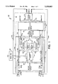
- FIG. 1 is a simplified block diagram of an integrated memory circuit constructed in accordance with the present invention.
- FIG. 2 is a schematic circuit diagram of an analog adding circuit used to implement the summing circuit of FIG. 1.
- FIG. 3 is a flow chart showing a preprogram verification operation in accordance with the present invention.
- FIG. 4A is a flow chart showing a two-cycle or low byte programming operation in accordance with the present invention as illustrated in FIG. 1 above.
- FIG. 4B is a flow chart showing one-cycle or word programming operation in accordance with the present invention as illustrated in FIG. 1 above.
- FIG. 5 is a flow chart showing a postprogram verification operation in accordance with the present invention as illustrated in FIG. 1 above.
- the present invention relates to a method and an integrated memory circuit for programming high density memory cells without undesirably increasing the number or the size of drain pumps formed on the integrated circuit.
- FIG. 1 illustrates an integrated memory circuit 100 constructed in accordance with the present invention.
- the integrated memory circuit 100 is responsive to an input data pattern DQ n (DQ 0 to DQ 15 ) which has 16 bits of information. Each bit is either at a first logic level or a second logic level. For the purpose of illustration, the first logic level is assumed to be a logic 0,while the second logic level is assumed to be a logic 1.
- the input data pattern DQ n is separated into two bytes, a low byte DQ na (DQ 0b to DQ 7a ) which represents the 0th to 7th bits and a high byte DQ nb (DQ 8b to DQ 15b ), which represents the 8th to 15thbits.
- the integrated memory circuit 100 includes a matrix of programmable memory cells.
- Each memory cell is used for storing 1 bit of information.
- the matrix of memory cells are organized into a plurality of blocks, and each block includes 2 groups of memory cells and each group includes 8 memory cells.
- each word is equivalent to one block; i.e., there are 256Kblocks.
- Each block is further divided into 2 groups of 8 bits each.
- Each bit is represented by 1 memory cell.
- FIG.1 only shows 1 block of memory cells 110.
- Memory cells block 110 includes 2 groups of memory cells 110a and 110b.
- Memory cells 110a and 110b each includes 8 memory cells.
- the integrated memory circuit 100 further includes a program mode determining circuit 112 for determining a program mode for programming block 110 in accordance with a number of the bits of the input data pattern DQ n and a programming circuit 113 operatively coupled to the program mode determining circuit 112 for programming block 110 according to its respective program mode.
- the number of the bitsof the input data pattern DQ n chosen for the purpose of program mode determination is 8, which is the number of memory cells a typical drain pump residing on the integrated memory circuit is able to supply simultaneously during programming.
- the program mode determining circuit 112 includes a memory cell determiningcircuit 114 for determining the total number of memory cells that is required to be programmed in block 110 and a control circuit 116 operatively coupled to the memory cell determining circuit 114 for providing a first program mode control signal if the total number of memory cells that is to be programmed in block 110 is greater than zero but is less than or equal to 8, a second program mode if the total number of memory cells that is required to be programmed in block 110 is more than 8, and a third program mode control signal if the total number of memory cells that is required to be programmed in block 110 is equal to zero.
- the memory cell determining circuit 114 includes a first comparator circuit118, a second comparator circuit 120 and a summing circuit 122.
- the first comparator circuit 118 is used for comparing the logic level of each bit of the input data pattern DQ n addressed to block 110 with the logic level of each of the memory cell in block 110.
- the second comparator circuit 120 is used for comparing the logic level of each bit of the input data pattern DQ n with the logic level of each corresponding bit stored in the memory cells, 110a and 110b, and providing a modified input data pattern DIM na (DIM Oa to DIM 7a ) and DIM nb (DIM 8b to DIM 15b ).
- Input data patterns DQ na and DQ nb are being applied to the secondcomparator 120.
- the second comparator 120 then generates data patterns DI na and DIM na .
- DI na is identical to DQ na and will be indicated as input data pattern in this embodiment.
- DIM na is a modified input data pattern as explained above.
- the second comparator 120 also provides data patterns DI nb and DIM nb .
- DI nb is identical to DQ nb and will be indicated as input data pattern in this embodiment.
- DIM nb is a modified input data pattern as explained above.
- DI na is coupled to the first comparator circuit 118 through line 124a.
- DI na or DIM na is selectively coupled to the summing circuit 122 through a selective switch 126a in the second comparator 120 across line 128a.
- DI nb is coupled to the first comparator circuit 118 through line 124b and DI nb or DIM nb is selectively coupled by switch 126b on line 128b to the summing circuit 122.
- Summing circuit 122 can be implemented by a digital adding circuit or an analog adding circuit.
- a typical digital adding circuit comprises a plurality of half and full digital adders to provide logical addition by summing the bits of the input data patterns DI na and DI nb or themodified input data patterns DIM na and DIM nb that are at logic 0.In this embodiment, 7 half digital adders and 19 full digital adders are used to accomplish the logic addition.
- a discussion on the implementation of digital adding circuit may be found in a book entitled "Circuit Design for CMOS VLSI," 1992, Pages 322-328, by John Uyemura.
- a typical analog adding circuit sums the current through a plurality of transistors.
- analog adding circuits are preferred because it is found that implementation of analog adding circuits here takes up less area on the integrated memory circuit than digital adding circuits.
- the summing circuit 122 computes the total number of bits of memory cells 110a and 110b that is required to be programmed by selectively summing thetotal number of bits of the input data patterns DQ na and DQ nb or the corresponding modified input data patterns DIM na and DIM na addressed to block 110 that are at logic 0 and then produces output signalX16PGM.
- the output signal X16PGM output signal will be at logic 1 when the number of memory cells that is required to be programmed is greater than zero but is less or equal to 8 and logic 0 when the total number of memorycells that is required to be programmed is greater than 8.
- Output signal X16PGM couples to control circuit 116 on line 130.
- the first comparator circuit 118 outputs signals LBMATCHP and HBMATCHP to control circuit 116 across lines 132a and 132b respectively.
- Control circuit 116 provides signal LBPGM and signal HBPGM to the second comparator circuit 120 across lines 134a and 134b respectively.
- Control circuit 116 provides a MATCH signal when the content of the memory cells 110a and 110b matches the contents of the input data pattern DQ n .
- the programming circuit 113 couples to drain pump 136. Drain pump 136 is coupled to a power supply VCC, typically at 5 volts.
- Memory cells 110a and110b couple to a plurality of decoders 138a and 138b respectively. Decoders138aand 138b couple to the programming circuit 113 via lines 140a and 140b respectively. Decoders 138acouple memory cells 110a through a first plurality of sense amplifiers 142a to the first comparator circuit 118. Similarly, decoders 138b couple memory cells 110b through a second plurality of sense amplifiers 142 b to the first comparator circuit 118. Sense amplifiers 142a and 142b provide data pattern DSI na and DSI nb respectively.
- Data pattern DSI na and DSI nb represent the contents of memory cells 110a and 110b respectively.
- Data pattern DSI na and DSI nb are being coupled to the second comparator circuit 120 on lines 144a and 144b respectively.
- the programming of integrated memory circuit 100 comprises three operations, namely a preprogram verification operation, a programming operation, and postprogramming verification operation. Immediately prior to the preprogram verification operation, memory cells 100a and 110b are assumed to have been fully erased, that is, they are all at logic 1.
- Summing circuit 122 uses the principle of a differential comparator circuits to provide for current summation.
- Summing circuit 122 comprises a plurality of transistors 210, 212, 214, 216, 218, 220, 222, 224, 226, 228, 230, 232, 234, 236, 238 and 240 coupled in parallel.
- the drain terminal of the plurality of transistors 210, 212, 214, 216, 218, 220, 222, 224, 226, 228,230, 232, 234, 236, 238 and 240 is coupled to a node 244 and a driver/buffer circuit 241.
- each of the plurality of transistors 210, 212, 214, 216, 218, 220, 222 and 224 is repsectively coupled to bit 0, 1, 2, 3, 4, 5, 6 and 7 of the input data patterns DI na or the modified input data pattern DIM na .
- the gate terminal of each of the plurality of transistors 226, 228, 230, 232, 234, 236, 238 and 240 is respectively coupled to bit 8, 9, 10, 11, 12, 13,14 and 15 of the input data pattern DI nb or the modified input data patterns DIM nb .
- each of the plurality of transistors 210, 212, 214, 216, 218, 220, 222, 224, 226, 228, 230, 232, 234, 236, 238 and 240 is coupled to the drain terminal of a current sourcetransistor 247.
- Current source transistor 247 has its gate terminal coupledto a voltage VBIAS and its source terminal coupled to power supply voltage VCC.
- Current source transistor 247 acts as a constant current source for the summing circuit 122.
- Each one of the plurality of transistors is turned on to allow current through the transistor when the corresponding bit coupled to the gate of that transistor is at logic 0.
- the total current through the plurality of transistors which is dependent on the total number of transistors being turned on, is then summed at point 244.
- the corresponding total voltage drop due to the total current is compared with a reference voltageV1 generated by a reference voltage generator 246 and an output signal X16PGM is provided via node 244 and driver/buffer circuit 241.
- the reference voltage V1 is selected such that the output signal X16PGM will be at logic 0 and logic 1 when the total number of logic 0 bits of the input data patterns DI na and DI nb (or the modified input data patterns DIM na and DIM nb ) is greater than 8 and less than or equal to 8 respectively.
- a program address and input data patterns DQ na and DQ nb are provided to the second comparator 120 via step 310.
- DQ na and DQ nb are being latched by second comparator circuit 120to provide signals DI na and DI nb respectively.
- the first comparator circuit 118 compares the input data patterns DI na and DI nb with the contents of the memory cells 110a and 110b respectively, and then output LBMATCHP signal and an HBMATCHP signal respectively via step 312.
- LBMATCHP will be at logic 0 whenever there is at least one bit in memory cells 110a that does not match with the corresponding bits of the input data pattern DQ na ; otherwise, LBMATCHP will be at logic 1.
- HBMATCHP will be at logic 0 whenever there is at least one bit in memory cells 110b that does not match with the corresponding bits of the input data pattern DQ nb ; otherwise, HBMATCHP will be at logic 1.
- step 314. it must be determined whether the contents of the memory cells 110a and 110b match the corresponding bit of the input data pattern DQ na and DQ nb via step 314. If each of the bits in the memory cells 110a and 110b matches with the corresponding bits of the input data pattern DQ na and DQ nb , the signals LBMATCHP and HBMATCHP will both be atlogic 1. In response, a MATCH signal which is at logic 1 will be provided by the control circuit 116 indicating that no programming is required via step 316. When the MATCH signal is at logic 1, it is also known as the third program mode control signal.
- the total number of bits that is required to be programmed must be determined via step 318.
- the summing circuit sums the number of bits of the input data patterns DQ na and DQ nb that are at logic 0 and generates output signal X16PGM.
- a bit of the input data patternDQ na or DQ nb is at logic 0, it indicates that programming of the corresponding bit in memory cells 110a or 110b is required, since all the bits in the memory cells 110a and 110b are presumed to have been erased, that is, they were all at logic 1, immediately prior to the preprogram verification operation.
- step 320 it must be determined whether the total number of bits required to beprogrammed is greater than 8 via step 320. If the total number of bits thatis required to be programmed is greater than 8, which is indicated by output signal X16PGM being at logic 0, a low byte or two-cycle programmingwill be performed via step 322. In case the total number of bits that is required to be programmed is greater than zero but is less than or equal to 8, then a word programming must be performed via step 324. In that case, both the high byte and the low byte will be programmed at the same time using one-cycle programming.
- FIG. 4A what is shown is a flow chart showing the operation of the two-cycle or low byte programming in accordance with the present invention as illustrated in FIG. 1 above.
- the control circuit 116 will provide an LBPGM signal which is at logic 1 and an HBPGM signal whichis at logic 0 via step 410.
- both the LBPGM signal and the HBPGM signal are being fed back to the second comparator circuit 120 across lines 134a and 134b respectively.
- the second comparator circuit 120 will trigger the programming circuit 113 so that it couples the drain pump 136 to memory cells 110a viastep 412.
- the second comparator 120 When the HBPGM signal is at logic 0, the second comparator 120 will not trigger the programming circuit 113 to couple the drain pump 136 to memory cells 110b. Accordingly, only memory cells 110a will be programmed.
- the drain pump 136 will be turned on for a fixed amount of time, for example, 15 microseconds, to allow for adequate programming of the memory cells 110a. The amount of time for programming is determinedthrough software or hardware (for example, by using a timer).
- the LBPGM signal will be switched from being at logic 1 to logic 0 after the amount of time set for programming has elapsed and programming can be stopped by allowing the programming circuit 113 to disconnect the drain pump 136 from the memory cells 110a via step 414. Thereafter, a postprogram verification operation will be performed via step 416 which will be further explained in FIG. 5.
- FIG. 4B what is shown is a flow chart for one-cycle or wordprogramming where all 16 bits are programmed simultaneously in accordance with the present invention as illustrated in FIG. 1 above.
- drain pump 136 When the numberof bits that are required to be programmed is less than 8, then drain pump 136 will be able to couple to all 16 bits simultaneously and provide the current needed since only those bits that require programming (bits that are at logic 0) draw current.
- the control circuit 116 will provide LBPGM and HBPGM signals which are at logic 1 via step 440.
- the second comparator circuit 120 triggers the programming circuit 113 to couple drain pump 136 to both memory cells 110a and 110b so that both memory cells 110a and 110b can be programmed at the same time via step 442.
- the programming of memory cells 110a and 110b will last for a certain amount of time, which can be determined through software or hardware (for example, by using a timer). After the desired time has elapsed, then LBPGM and HBPGM signals will be reset to logic 0 and programming can be stopped by allowing the programming circuit 113 to disconnect the drain pump 136 from the memory cells 110a and 110b via step444. Thereafter, a postprogram verification operation 416 will be performedwhich will be further explained in FIG. 5.
- FIG. 5 what is shown is a postprogram verification operation of the integrated memory circuit 100 as illustrated in FIG. 1.
- the second comparator 120 provides modified input data pattern DIM na and DIM nb via step 510.
- memory cells 110a and 110b are assumed to have been fully erased, that is, they are all at logic 1. After the preprogram verification and programming operations, the number of bits that is still required to be programmed must be determined. A comparison between each corresponding bit of the memory cells 110a (or 110b) and the input data patterns DQ na are made to provide DIM na (or DIM nb ).
- DIM na (or DIM nb ) has bits of information identical to the input pattern DQ na (or DQ nb ) except that if a bit in the input data pattern DQ na (or DQ nb ) and the corresponding bit in the memory cells 110a (or 110b), represented by DSI na (or DSI nb ) are both at logic 0, then the corresponding bitin the DIM na (or DIM nb ) will be at logic 1. When DIM na (or DIM nb ) is at logic 1, it indicates that no further programming is required for that bit.
- the number of memory cells that is required to be programmed after the preprogram verification and programming operation can be determined by summing the total number ofbits of the modified input data patterns DIM na and DIM nb that areat logic 0.
- step512 it must be determined whether all the bits in memory cells 110a and 110b matches with the input data patterns DQ na and DQ nb via step512. If they match, the control circuit 116 will output the third program mode control signal, represented by the MATCH signal which is at logic 1, via step 514. In this case, no further programming is required.
- step 512 determines that the contents of some of the memory cells, as represented by DSI na or DSI nb , do not match with the corresponding bits of the input data patterns DQ na or DQ nb , the total number of bits that is required to be programmed must be determined.
- the summing circuit 1 22 computes the number of bits that is still requiredto be programmed by summing the number of bits of the modified input data pattern DIM na and DIM nb that are at logic 0 via step 516. Thereafter, it must be determined whether the total number of bits to be programmed is greater than 8 via step 518.
- step 520 a low byte programming can be performed via step 520 which is similar to what is illustrated in the flow chart of FIG. 4A.
- a word programming can be performed via step 522 which issimilar to what is illustrated in the flow chart of FIG. 4B.
- the programming and postprogram verification operation can be repeated until it is determined that each of the bit in the memory cells 110a and 110b matches those in the input data pattern DQ na When that happens, the memory cells 110a and 110b are said to have been programmed according to the input data pattern DQ n .
- an integrated memory circuit which has a plurality of memory cells can be programmed effectively by providing a program mode for programming the memory cells in accordance with a number of bits of the input data pattern and then programming the memory cells in accordance with the program mode so provided. In so doing,it avoids the undesirable increase in the number or the current capacity ofdrain pumps formed on such memory circuits thus reducing the complexity of the design and minimizing the size of the memory circuit.
- the above described embodiment is merely illustrating the possible specific embodiment which can represent application of the principles of the present invention.
- the number of bits to be programmed in a one-cycle programming can be adjustedto other values, such as 4.
- the total number of cycles for the programming operation can be varied as required, for example, depending onthe density of the integrated memory circuit. For instance, a 32 Mbit flashEPROM organized as 1 million blocks of 32 bits each may be programmed using a one-cycle, two-cycle, three-cycle and four-cycle programming. In that case, a conventional drain pump with current capacity to program 8 bits simultaneously may be used.
Abstract
Description
Claims (30)
Priority Applications (7)
| Application Number | Priority Date | Filing Date | Title |
|---|---|---|---|
| US08/227,755 US5530803A (en) | 1994-04-14 | 1994-04-14 | Method and apparatus for programming memory devices |
| TW083106797A TW332292B (en) | 1994-04-14 | 1994-07-26 | Method and apparatus for programming memory devices |
| DE69520853T DE69520853T2 (en) | 1994-04-14 | 1995-03-23 | Method and device for programming memory arrangements |
| AT95301953T ATE201111T1 (en) | 1994-04-14 | 1995-03-23 | METHOD AND DEVICE FOR PROGRAMMING MEMORY ARRANGEMENTS |
| EP95301953A EP0677850B1 (en) | 1994-04-14 | 1995-03-23 | Method and apparatus for programming memory devices |
| KR1019950008213A KR100357443B1 (en) | 1994-04-14 | 1995-04-08 | Memory device programming method and device |
| JP08668595A JP3741744B2 (en) | 1994-04-14 | 1995-04-12 | Memory integrated circuit and memory cell programming method |
Applications Claiming Priority (1)
| Application Number | Priority Date | Filing Date | Title |
|---|---|---|---|
| US08/227,755 US5530803A (en) | 1994-04-14 | 1994-04-14 | Method and apparatus for programming memory devices |
Publications (1)
| Publication Number | Publication Date |
|---|---|
| US5530803A true US5530803A (en) | 1996-06-25 |
Family
ID=22854328
Family Applications (1)
| Application Number | Title | Priority Date | Filing Date |
|---|---|---|---|
| US08/227,755 Expired - Lifetime US5530803A (en) | 1994-04-14 | 1994-04-14 | Method and apparatus for programming memory devices |
Country Status (7)
| Country | Link |
|---|---|
| US (1) | US5530803A (en) |
| EP (1) | EP0677850B1 (en) |
| JP (1) | JP3741744B2 (en) |
| KR (1) | KR100357443B1 (en) |
| AT (1) | ATE201111T1 (en) |
| DE (1) | DE69520853T2 (en) |
| TW (1) | TW332292B (en) |
Cited By (25)
| Publication number | Priority date | Publication date | Assignee | Title |
|---|---|---|---|---|
| US20020194422A1 (en) * | 2001-04-05 | 2002-12-19 | Zeev Cohen | Method and apparatus for dynamically masking an N-bit memory array having individually programmable cells |
| KR100393595B1 (en) * | 2001-08-27 | 2003-08-02 | 엘지전자 주식회사 | Memory Programming System and Method for the Same |
| US20040153620A1 (en) * | 2003-01-30 | 2004-08-05 | Shai Eisen | Address scramble |
| US20040222437A1 (en) * | 2000-12-07 | 2004-11-11 | Dror Avni | Programming and erasing methods for an NROM array |
| US20050058005A1 (en) * | 2002-01-31 | 2005-03-17 | Assaf Shappir | Method for operating a memory device |
| US20050117395A1 (en) * | 2002-01-31 | 2005-06-02 | Saifun Semiconductors Ltd. | Method for operating a memory device |
| US6917544B2 (en) | 2002-07-10 | 2005-07-12 | Saifun Semiconductors Ltd. | Multiple use memory chip |
| US20050276118A1 (en) * | 2004-06-10 | 2005-12-15 | Eduardo Maayan | Reduced power programming of non-volatile cells |
| US7064983B2 (en) | 2001-04-05 | 2006-06-20 | Saifum Semiconductors Ltd. | Method for programming a reference cell |
| US7136304B2 (en) | 2002-10-29 | 2006-11-14 | Saifun Semiconductor Ltd | Method, system and circuit for programming a non-volatile memory array |
| US20070183205A1 (en) * | 2006-02-03 | 2007-08-09 | Samsung Electronics Co., Ltd. | Semiconductor memory device controlling program voltage according to the number of cells to be programmed and method of programming the same |
| US7590001B2 (en) | 2007-12-18 | 2009-09-15 | Saifun Semiconductors Ltd. | Flash memory with optimized write sector spares |
| US7652930B2 (en) | 2004-04-01 | 2010-01-26 | Saifun Semiconductors Ltd. | Method, circuit and system for erasing one or more non-volatile memory cells |
| US7668017B2 (en) | 2005-08-17 | 2010-02-23 | Saifun Semiconductors Ltd. | Method of erasing non-volatile memory cells |
| US7692961B2 (en) | 2006-02-21 | 2010-04-06 | Saifun Semiconductors Ltd. | Method, circuit and device for disturb-control of programming nonvolatile memory cells by hot-hole injection (HHI) and by channel hot-electron (CHE) injection |
| US7701779B2 (en) | 2006-04-27 | 2010-04-20 | Sajfun Semiconductors Ltd. | Method for programming a reference cell |
| US7743230B2 (en) | 2003-01-31 | 2010-06-22 | Saifun Semiconductors Ltd. | Memory array programming circuit and a method for using the circuit |
| US7760554B2 (en) | 2006-02-21 | 2010-07-20 | Saifun Semiconductors Ltd. | NROM non-volatile memory and mode of operation |
| US7786512B2 (en) | 2005-07-18 | 2010-08-31 | Saifun Semiconductors Ltd. | Dense non-volatile memory array and method of fabrication |
| US7808818B2 (en) | 2006-01-12 | 2010-10-05 | Saifun Semiconductors Ltd. | Secondary injection for NROM |
| US7964459B2 (en) | 2004-10-14 | 2011-06-21 | Spansion Israel Ltd. | Non-volatile memory structure and method of fabrication |
| US8053812B2 (en) | 2005-03-17 | 2011-11-08 | Spansion Israel Ltd | Contact in planar NROM technology |
| US8253452B2 (en) | 2006-02-21 | 2012-08-28 | Spansion Israel Ltd | Circuit and method for powering up an integrated circuit and an integrated circuit utilizing same |
| US8400841B2 (en) | 2005-06-15 | 2013-03-19 | Spansion Israel Ltd. | Device to program adjacent storage cells of different NROM cells |
| EP1927115B1 (en) * | 2005-09-20 | 2015-11-18 | Cypress Semiconductor Corporation | High performance flash memory device using a programming window for predetermination of bits to be programmed |
Families Citing this family (4)
| Publication number | Priority date | Publication date | Assignee | Title |
|---|---|---|---|---|
| US5787039A (en) * | 1997-03-06 | 1998-07-28 | Macronix International Co., Ltd. | Low current floating gate programming with bit-by-bit verification |
| JP3156636B2 (en) * | 1997-05-30 | 2001-04-16 | 日本電気株式会社 | Nonvolatile semiconductor memory device |
| TWI308692B (en) | 2005-10-26 | 2009-04-11 | Sunplus Technology Co Ltd | Programmable memory and accessing method of the same |
| US8570828B2 (en) * | 2010-04-12 | 2013-10-29 | Mosaid Technologies Incorporated | Memory programming using variable data width |
Citations (8)
| Publication number | Priority date | Publication date | Assignee | Title |
|---|---|---|---|---|
| US4701886A (en) * | 1984-08-22 | 1987-10-20 | Hitachi, Ltd. | Semiconductor integrated circuit device |
| US4729117A (en) * | 1985-03-20 | 1988-03-01 | Kabushiki Kaisha Toshiba | Semiconductor memory device |
| US4841233A (en) * | 1985-06-20 | 1989-06-20 | Fujitsu Limited | Semiconductor integrated circuit adapted to carry out operation test |
| US4862418A (en) * | 1986-01-20 | 1989-08-29 | U.S. Philips Corp. | Non-volatile, programmable semiconductor memory having reduced testing time |
| US4905191A (en) * | 1987-01-16 | 1990-02-27 | Hitachi Ltd. | Microcomputer with built-in EPROM and test mode |
| US5091910A (en) * | 1989-01-24 | 1992-02-25 | Ricoh Company, Ltd. | Information processing device |
| US5224103A (en) * | 1990-07-16 | 1993-06-29 | North American Philips Corporation | Processing device and method of programming such a processing device |
| US5228000A (en) * | 1990-08-02 | 1993-07-13 | Mitsubishi Denki Kabushiki Kaisha | Test circuit of semiconductor memory device |
Family Cites Families (4)
| Publication number | Priority date | Publication date | Assignee | Title |
|---|---|---|---|---|
| US4763305A (en) * | 1985-11-27 | 1988-08-09 | Motorola, Inc. | Intelligent write in an EEPROM with data and erase check |
| JP2900523B2 (en) * | 1990-05-31 | 1999-06-02 | 日本電気株式会社 | Write circuit for nonvolatile semiconductor memory device |
| KR960002006B1 (en) * | 1991-03-12 | 1996-02-09 | 가부시끼가이샤 도시바 | Eeprom with write/verify controller using two reference levels |
| JPH06267283A (en) * | 1993-03-16 | 1994-09-22 | Mitsubishi Electric Corp | Read-only memory writable data and method for writing/ reading data |
-
1994
- 1994-04-14 US US08/227,755 patent/US5530803A/en not_active Expired - Lifetime
- 1994-07-26 TW TW083106797A patent/TW332292B/en not_active IP Right Cessation
-
1995
- 1995-03-23 EP EP95301953A patent/EP0677850B1/en not_active Expired - Lifetime
- 1995-03-23 AT AT95301953T patent/ATE201111T1/en not_active IP Right Cessation
- 1995-03-23 DE DE69520853T patent/DE69520853T2/en not_active Expired - Lifetime
- 1995-04-08 KR KR1019950008213A patent/KR100357443B1/en not_active IP Right Cessation
- 1995-04-12 JP JP08668595A patent/JP3741744B2/en not_active Expired - Lifetime
Patent Citations (8)
| Publication number | Priority date | Publication date | Assignee | Title |
|---|---|---|---|---|
| US4701886A (en) * | 1984-08-22 | 1987-10-20 | Hitachi, Ltd. | Semiconductor integrated circuit device |
| US4729117A (en) * | 1985-03-20 | 1988-03-01 | Kabushiki Kaisha Toshiba | Semiconductor memory device |
| US4841233A (en) * | 1985-06-20 | 1989-06-20 | Fujitsu Limited | Semiconductor integrated circuit adapted to carry out operation test |
| US4862418A (en) * | 1986-01-20 | 1989-08-29 | U.S. Philips Corp. | Non-volatile, programmable semiconductor memory having reduced testing time |
| US4905191A (en) * | 1987-01-16 | 1990-02-27 | Hitachi Ltd. | Microcomputer with built-in EPROM and test mode |
| US5091910A (en) * | 1989-01-24 | 1992-02-25 | Ricoh Company, Ltd. | Information processing device |
| US5224103A (en) * | 1990-07-16 | 1993-06-29 | North American Philips Corporation | Processing device and method of programming such a processing device |
| US5228000A (en) * | 1990-08-02 | 1993-07-13 | Mitsubishi Denki Kabushiki Kaisha | Test circuit of semiconductor memory device |
Non-Patent Citations (4)
| Title |
|---|
| I. S. Hwang and A. L. Fisher, "Ultrafact Compact 32-bit CMOS in Multiple-Output Domino Logic", IEEE Journal of Solid State Circuits, vol. 24, No. 2, Apr. 1989, pp. 358-369. |
| I. S. Hwang and A. L. Fisher, Ultrafact Compact 32 bit CMOS in Multiple Output Domino Logic , IEEE Journal of Solid State Circuits, vol. 24, No. 2, Apr. 1989, pp. 358 369. * |
| John P. Uyemura, "Circuit Design for CMOS VLSI", 1992, pp. 322-328. |
| John P. Uyemura, Circuit Design for CMOS VLSI , 1992, pp. 322 328. * |
Cited By (35)
| Publication number | Priority date | Publication date | Assignee | Title |
|---|---|---|---|---|
| US6937521B2 (en) | 2000-05-04 | 2005-08-30 | Saifun Semiconductors Ltd. | Programming and erasing methods for a non-volatile memory cell |
| US6928001B2 (en) | 2000-12-07 | 2005-08-09 | Saifun Semiconductors Ltd. | Programming and erasing methods for a non-volatile memory cell |
| US20040222437A1 (en) * | 2000-12-07 | 2004-11-11 | Dror Avni | Programming and erasing methods for an NROM array |
| US6665769B2 (en) * | 2001-04-05 | 2003-12-16 | Saifun Semiconductors Ltd. | Method and apparatus for dynamically masking an N-bit memory array having individually programmable cells |
| US7064983B2 (en) | 2001-04-05 | 2006-06-20 | Saifum Semiconductors Ltd. | Method for programming a reference cell |
| US20020194422A1 (en) * | 2001-04-05 | 2002-12-19 | Zeev Cohen | Method and apparatus for dynamically masking an N-bit memory array having individually programmable cells |
| KR100393595B1 (en) * | 2001-08-27 | 2003-08-02 | 엘지전자 주식회사 | Memory Programming System and Method for the Same |
| US20050117395A1 (en) * | 2002-01-31 | 2005-06-02 | Saifun Semiconductors Ltd. | Method for operating a memory device |
| US7079420B2 (en) | 2002-01-31 | 2006-07-18 | Saifun Semiconductors Ltd. | Method for operating a memory device |
| US20050058005A1 (en) * | 2002-01-31 | 2005-03-17 | Assaf Shappir | Method for operating a memory device |
| US7190620B2 (en) | 2002-01-31 | 2007-03-13 | Saifun Semiconductors Ltd. | Method for operating a memory device |
| US6917544B2 (en) | 2002-07-10 | 2005-07-12 | Saifun Semiconductors Ltd. | Multiple use memory chip |
| US7738304B2 (en) | 2002-07-10 | 2010-06-15 | Saifun Semiconductors Ltd. | Multiple use memory chip |
| US7136304B2 (en) | 2002-10-29 | 2006-11-14 | Saifun Semiconductor Ltd | Method, system and circuit for programming a non-volatile memory array |
| US7675782B2 (en) | 2002-10-29 | 2010-03-09 | Saifun Semiconductors Ltd. | Method, system and circuit for programming a non-volatile memory array |
| US6967896B2 (en) | 2003-01-30 | 2005-11-22 | Saifun Semiconductors Ltd | Address scramble |
| US20040153620A1 (en) * | 2003-01-30 | 2004-08-05 | Shai Eisen | Address scramble |
| US7743230B2 (en) | 2003-01-31 | 2010-06-22 | Saifun Semiconductors Ltd. | Memory array programming circuit and a method for using the circuit |
| US7652930B2 (en) | 2004-04-01 | 2010-01-26 | Saifun Semiconductors Ltd. | Method, circuit and system for erasing one or more non-volatile memory cells |
| US20050276118A1 (en) * | 2004-06-10 | 2005-12-15 | Eduardo Maayan | Reduced power programming of non-volatile cells |
| US7366025B2 (en) | 2004-06-10 | 2008-04-29 | Saifun Semiconductors Ltd. | Reduced power programming of non-volatile cells |
| US7964459B2 (en) | 2004-10-14 | 2011-06-21 | Spansion Israel Ltd. | Non-volatile memory structure and method of fabrication |
| US8053812B2 (en) | 2005-03-17 | 2011-11-08 | Spansion Israel Ltd | Contact in planar NROM technology |
| US8400841B2 (en) | 2005-06-15 | 2013-03-19 | Spansion Israel Ltd. | Device to program adjacent storage cells of different NROM cells |
| US7786512B2 (en) | 2005-07-18 | 2010-08-31 | Saifun Semiconductors Ltd. | Dense non-volatile memory array and method of fabrication |
| US7668017B2 (en) | 2005-08-17 | 2010-02-23 | Saifun Semiconductors Ltd. | Method of erasing non-volatile memory cells |
| EP1927115B1 (en) * | 2005-09-20 | 2015-11-18 | Cypress Semiconductor Corporation | High performance flash memory device using a programming window for predetermination of bits to be programmed |
| US7808818B2 (en) | 2006-01-12 | 2010-10-05 | Saifun Semiconductors Ltd. | Secondary injection for NROM |
| US20070183205A1 (en) * | 2006-02-03 | 2007-08-09 | Samsung Electronics Co., Ltd. | Semiconductor memory device controlling program voltage according to the number of cells to be programmed and method of programming the same |
| US7679964B2 (en) | 2006-02-03 | 2010-03-16 | Samsung Electronics Co., Ltd. | Semiconductor memory device controlling program voltage according to the number of cells to be programmed and method of programming the same |
| US7760554B2 (en) | 2006-02-21 | 2010-07-20 | Saifun Semiconductors Ltd. | NROM non-volatile memory and mode of operation |
| US7692961B2 (en) | 2006-02-21 | 2010-04-06 | Saifun Semiconductors Ltd. | Method, circuit and device for disturb-control of programming nonvolatile memory cells by hot-hole injection (HHI) and by channel hot-electron (CHE) injection |
| US8253452B2 (en) | 2006-02-21 | 2012-08-28 | Spansion Israel Ltd | Circuit and method for powering up an integrated circuit and an integrated circuit utilizing same |
| US7701779B2 (en) | 2006-04-27 | 2010-04-20 | Sajfun Semiconductors Ltd. | Method for programming a reference cell |
| US7590001B2 (en) | 2007-12-18 | 2009-09-15 | Saifun Semiconductors Ltd. | Flash memory with optimized write sector spares |
Also Published As
| Publication number | Publication date |
|---|---|
| KR950033835A (en) | 1995-12-26 |
| ATE201111T1 (en) | 2001-05-15 |
| EP0677850B1 (en) | 2001-05-09 |
| KR100357443B1 (en) | 2002-12-12 |
| EP0677850A2 (en) | 1995-10-18 |
| JP3741744B2 (en) | 2006-02-01 |
| TW332292B (en) | 1998-05-21 |
| JPH0845290A (en) | 1996-02-16 |
| EP0677850A3 (en) | 1996-12-11 |
| DE69520853D1 (en) | 2001-06-13 |
| DE69520853T2 (en) | 2001-12-20 |
Similar Documents
| Publication | Publication Date | Title |
|---|---|---|
| US5530803A (en) | Method and apparatus for programming memory devices | |
| US5475634A (en) | Floating gate memory array with latches having improved immunity to write disturbance, and with storage latches | |
| KR100292661B1 (en) | Bitmap Addressing System for Flash Memory | |
| JP2648840B2 (en) | Semiconductor storage device | |
| US20140355342A1 (en) | Dynamically configurable mlc state assignment | |
| US7949823B2 (en) | Multilevel storage nonvolatile semiconductor memory device enabling high-speed data reading and high-speed data writing | |
| US20140149648A1 (en) | Memory system with user configurable density/performance option | |
| US6011720A (en) | Nonvolatile memory with reduced write time/write verify time and semiconductor device thereof | |
| KR20040067195A (en) | Page buffer for NAND flash memory | |
| JP2000251484A (en) | Non-volatile semiconductor memory | |
| US7248503B2 (en) | Semiconductor nonvolatile storage device | |
| US5293350A (en) | Nonvolatile semiconductor memory device | |
| WO1983001146A1 (en) | Eeprom with bulk zero program capability | |
| US6134149A (en) | Method and apparatus for reducing high current during chip erase in flash memories | |
| JP2000082293A (en) | Method and device for writing in erasable nonvolatile memory | |
| US5617350A (en) | Flash memory system having reduced disturb and method | |
| US7532510B2 (en) | Flash memory device with sector access | |
| US6185128B1 (en) | Reference cell four-way switch for a simultaneous operation flash memory device | |
| US6611456B2 (en) | Method and apparatus for reducing the number of programmed bits in a memory array | |
| EP0945874B1 (en) | Nonvolatile semiconductor memory device | |
| US6859391B1 (en) | EEPROM architecture and programming protocol | |
| US6587373B2 (en) | Multilevel cell memory architecture | |
| WO1997022971A9 (en) | A negative voltage switch architecture for a nonvolatile memory | |
| KR20030063186A (en) | Method for writing data bits to a memory array | |
| JP4294977B2 (en) | Nonvolatile storage device |
Legal Events
| Date | Code | Title | Description |
|---|---|---|---|
| AS | Assignment |
Owner name: ADVANCED MICRO DEVICES, INC., CALIFORNIA Free format text: ASSIGNMENT OF ASSIGNORS INTEREST;ASSIGNORS:CHANG, GEORGE;CHENG, PEARL;REEL/FRAME:006963/0597 Effective date: 19940413 |
|
| STCF | Information on status: patent grant |
Free format text: PATENTED CASE |
|
| FPAY | Fee payment |
Year of fee payment: 4 |
|
| FPAY | Fee payment |
Year of fee payment: 8 |
|
| AS | Assignment |
Owner name: SPANSION INC., CALIFORNIA Free format text: ASSIGNMENT OF ASSIGNORS INTEREST;ASSIGNOR:ADVANCED MICRO DEVICES, INC.;REEL/FRAME:019028/0599 Effective date: 20070131 |
|
| AS | Assignment |
Owner name: SPANSION LLC, CALIFORNIA Free format text: ASSIGNMENT OF ASSIGNORS INTEREST;ASSIGNOR:SPANSION INC.;REEL/FRAME:019063/0771 Effective date: 20070131 |
|
| FPAY | Fee payment |
Year of fee payment: 12 |
|
| AS | Assignment |
Owner name: BARCLAYS BANK PLC,NEW YORK Free format text: SECURITY AGREEMENT;ASSIGNORS:SPANSION LLC;SPANSION INC.;SPANSION TECHNOLOGY INC.;AND OTHERS;REEL/FRAME:024522/0338 Effective date: 20100510 Owner name: BARCLAYS BANK PLC, NEW YORK Free format text: SECURITY AGREEMENT;ASSIGNORS:SPANSION LLC;SPANSION INC.;SPANSION TECHNOLOGY INC.;AND OTHERS;REEL/FRAME:024522/0338 Effective date: 20100510 |
|
| AS | Assignment |
Owner name: SPANSION TECHNOLOGY LLC, CALIFORNIA Free format text: RELEASE BY SECURED PARTY;ASSIGNOR:BARCLAYS BANK PLC;REEL/FRAME:035201/0159 Effective date: 20150312 Owner name: SPANSION INC., CALIFORNIA Free format text: RELEASE BY SECURED PARTY;ASSIGNOR:BARCLAYS BANK PLC;REEL/FRAME:035201/0159 Effective date: 20150312 Owner name: SPANSION LLC, CALIFORNIA Free format text: RELEASE BY SECURED PARTY;ASSIGNOR:BARCLAYS BANK PLC;REEL/FRAME:035201/0159 Effective date: 20150312 |
|
| AS | Assignment |
Owner name: MORGAN STANLEY SENIOR FUNDING, INC., NEW YORK Free format text: SECURITY INTEREST;ASSIGNORS:CYPRESS SEMICONDUCTOR CORPORATION;SPANSION LLC;REEL/FRAME:035240/0429 Effective date: 20150312 |
|
| AS | Assignment |
Owner name: CYPRESS SEMICONDUCTOR CORPORATION, CALIFORNIA Free format text: ASSIGNMENT OF ASSIGNORS INTEREST;ASSIGNOR:SPANSION, LLC;REEL/FRAME:036018/0546 Effective date: 20150601 |
|
| AS | Assignment |
Owner name: MORGAN STANLEY SENIOR FUNDING, INC., NEW YORK Free format text: CORRECTIVE ASSIGNMENT TO CORRECT THE 8647899 PREVIOUSLY RECORDED ON REEL 035240 FRAME 0429. ASSIGNOR(S) HEREBY CONFIRMS THE SECURITY INTERST;ASSIGNORS:CYPRESS SEMICONDUCTOR CORPORATION;SPANSION LLC;REEL/FRAME:058002/0470 Effective date: 20150312 |