US5574668A - Apparatus and method for measuring ball grid arrays - Google Patents
Apparatus and method for measuring ball grid arrays Download PDFInfo
- Publication number
- US5574668A US5574668A US08/394,642 US39464295A US5574668A US 5574668 A US5574668 A US 5574668A US 39464295 A US39464295 A US 39464295A US 5574668 A US5574668 A US 5574668A
- Authority
- US
- United States
- Prior art keywords
- ball grid
- grid array
- touch sensor
- array
- contact
- Prior art date
- Legal status (The legal status is an assumption and is not a legal conclusion. Google has not performed a legal analysis and makes no representation as to the accuracy of the status listed.)
- Expired - Fee Related
Links
Images


Classifications
-
- G—PHYSICS
- G01—MEASURING; TESTING
- G01B—MEASURING LENGTH, THICKNESS OR SIMILAR LINEAR DIMENSIONS; MEASURING ANGLES; MEASURING AREAS; MEASURING IRREGULARITIES OF SURFACES OR CONTOURS
- G01B7/00—Measuring arrangements characterised by the use of electric or magnetic techniques
- G01B7/34—Measuring arrangements characterised by the use of electric or magnetic techniques for measuring roughness or irregularity of surfaces
- G01B7/345—Measuring arrangements characterised by the use of electric or magnetic techniques for measuring roughness or irregularity of surfaces for measuring evenness
-
- G—PHYSICS
- G01—MEASURING; TESTING
- G01B—MEASURING LENGTH, THICKNESS OR SIMILAR LINEAR DIMENSIONS; MEASURING ANGLES; MEASURING AREAS; MEASURING IRREGULARITIES OF SURFACES OR CONTOURS
- G01B21/00—Measuring arrangements or details thereof, where the measuring technique is not covered by the other groups of this subclass, unspecified or not relevant
- G01B21/02—Measuring arrangements or details thereof, where the measuring technique is not covered by the other groups of this subclass, unspecified or not relevant for measuring length, width, or thickness
- G01B21/04—Measuring arrangements or details thereof, where the measuring technique is not covered by the other groups of this subclass, unspecified or not relevant for measuring length, width, or thickness by measuring coordinates of points
Definitions
- This invention relates to an apparatus for inspecting ball grid arrays and, more particularly, to a computer controlled gas pressure-backed, touch sensor array apparatus.
- a ball grid array is an array of solderable balls placed on a chip carrier. The balls contact a printed circuit board in an array configuration where, after reheat, they connect the chip to the printed circuit board.
- BGAs are known with 40, 50 and 60 mil. spacings in regular and staggered array patterns.
- the prior art does not provide an automated means for measuring the height of the balls on top of the ball grid array, does not have a means for determining the flatness of the ball grid array, nor does it have a means for determining whether the balls have been properly formed or exist at all in their proper positions.
- the invention provides a linear motion actuator that precisely moves a stage. Attached to the stage is a sensor assembly comprising an array of touch sensors.
- the linear motion actuator moves the stage to contact the actuators on a ball grid array that has been moved under the stage.
- a rotary tray of ball grid arrays are loaded from a storage tray, inspected, and unloaded to a pass tray or a fail tray.
- the touch sensor is composed of a conductive disk having an insulated shaft through the center.
- the insulated shaft is aligned with an alignment plate and protrudes through the bottom of a sensor plate.
- the conductive disks are provided to open or close a circuit, depending upon the state of the touch sensor. If the touch sensor contacts a ball as it is descending toward the BGA, the ball will push the sensor and break an electrical connection.
- a computer scans the array to determine if any circuit has been broken, if it has the computer stores in a memory the particular location of the break and the position of the stage assembly at the time of the break.
- the sensors are impressed against the sensor plate by air pressure. The air is kept clean and dry to prevent dust or debris from entering the interior cavity of the sensor.
- FIG. 1A shows a schematic block diagram of the ball grid array inspection system of the invention.
- FIG. 1B shows a seating plane diagram
- FIG. 1C shows a ball center error chart.
- FIG. 1D shows a pitch diagram for the ball grid array.
- FIG. 1E shows a ball center error diagram
- FIG. 1F shows a board warpage diagram
- FIG. 1G shows a ball array of the ball grid array showing best fit reference coordinates.
- FIG. 2A shows a detailed drawing of a touch sensor of the invention.
- FIG. 2B shows a top down diagram of a tripod mount of the sensors of the invention.
- FIG. 2C shows a more detailed circuit diagram of one embodiment of a probe switch array of the invention.
- FIG. 3A shows a circular ridge contact configuration
- FIG. 3B shows a linear contact ridge configuration
- FIG. 4 shows a schematic block diagram of the scanning electronics of the invention.
- FIG. 5A shows a schematic diagram of a system employing multiple ball grid array inspection stations on a circular cart carriage.
- FIG. 5B shows a portion of a ball grid array.
- FIG. 6 shows an inspection system control screen.
- FIG. 7 shows the inspection system part definition screen.
- FIG. 8 shows a tray definition screen
- FIG. 9 shows a tolerance screen
- FIG. 10 shows a graph of the results of a single probe of the invention stepped and repeated across a ball grid array.
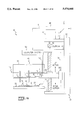
- FIG. 1A shows a schematic diagram of an apparatus to inspect ball grid arrays built in accordance with the teachings of the invention.
- Stage actuator 24 is comprised of a base 26 which holds a lower bearing 41 and an upper bearing 40 and rail 38.
- a linear slide 36 rides up and down rail 38.
- the screw 34 drives stage 32, connected to slide 36, on rail 38.
- the coupler 42 couples the screw 34 to motor 44 which, in one embodiment, may be a servo motor, and in an alternative embodiment may comprise a stepper motor.
- Position sensor 46 determines the rotational position of the screw 34 which may be converted into a linear position using conventional means.
- the linear position of the stage 32 can also be determined by a linear encoder positioned on the rail 38.
- the position of the stage is sent to the computer system 50 on line 51.
- Computer system 50 receives the signals from the touch sensors through cable 52.
- Computer system 50 is shown in more detail in FIG. 4.
- Attached to the stage 32 is a sensor assembly 54 comprising a housing 30 where air pressure inlet 48 provides positive air pressure to the interior of the housing 30.
- An alignment plate 11 provides guidance for touch sensors 12 which protrude through the base plate 28.
- the base plate 28 is a printed circuit board, the structure of which is shown in more detail in FIG. 2A.
- the ball grid array 14 is comprised of a ball 18 made of solderable material, a substrate 20 and an integrated circuit 21.
- the stage 32 is driven by screw 34 until the balls on the ball grid array have been touched. While the stage is moving down, touch sensors indicate that a ball has not been touched by providing a closed signal, and indicates that a ball has been touched by providing an open signal to the computer system 50. In this way as switches are opened by the presence of balls on the ball grid array, the computer notes the position of the encoder thus determining the position of each ball on the ball grid array.
- the BGA 14 may be moved in relation to the sensor assembly 54 to measure the surface of the substrate 20.
- a hydraulic or pneumatic lift can be provided where the stage 32 is lifted and then dropped. As the stage is dropped the touch sensor array is scanned as described above.
- FIG. 1B illustrates a method used to determined coplanarity of a ball grid array 14.
- the ball grid array 14 defines a seating plane 102 as a least squares plane or an ideal seating plane.
- the data of distance of the crown of each ball 18 from the entire ball grid array 14 above the substrate 20 defines the least squares plane.
- the distance of each individual crown of each ball 18 above or below the seating plane 102 determines a coplanarity 104 of that ball.
- FIG. 1C illustrates deviation of the center of a ball from ideal in the plane of the integrated circuit 21.
- a ball 18 has a ball center 106. Deviation along the X-axis 108 from an ideal center 116 defines X ball error 112. Deviation along the Y-axis 110 from an ideal center 116 defines Y ball error 114.
- FIG. 1D shows a pitch diagram for the ball grid array 14.
- the distance between the centers 106 of two adjacent balls 18 along the X axis 108 defines X PITCH (Xpitch) 118.
- the distance between the centers 106 of two adjacent balls 18 along the Y axis 110 defines Y PITCH (Ypitch) 120.
- the top edge of the ball grid array 14 is defined as -A- datum 122.
- the right edge of the ball grid array 14 is defined as -B- datum 124.
- the distance from the- A- datum 122 to the center of the center ball in the last row, or a center gap for an even number of rows of balls defines an -A- DATUM OFFSET 126.
- the distance from the -B- datum 124 to the center of the center ball in the last column, or a center gap for even number of columns of balls defines -B- DATUM OFFSET 128.
- FIG. 1E illustrates determination of radial error.
- the distance between the ideal center 116 and the actual center 106 of a ball 18 defines radial error (Rerr) 130.
- This measurement may be used to define the tolerance of the center location 106 of a ball 18 from the ideal center 116.
- a circle of radius "R" 132 centered on the ideal ball location 116 may define the tolerance for the location of the center 106 of a ball 18. If the center 106 of a measured ball 18 lies outside of the circle 132, the ball grid array 14 fails.
- FIG. 1F shows an illustration of board warpage.
- the deviation of the substrate from a plane may be determined.
- the deviation may be determined from the average of the five highest readings minus the minimum board reading as determined from the average of the five lowest readings defines board warpage 140.
- the board can have both positive curvature 142 and negative curvature 144.
- the X-axis 108 may be defined to be the best line fit to the centers of the middle column of balls 150, or to the centers of the gaps between the two middle columns of balls in the case of an even number of columns.
- the Y-axis 110 may be defined to be the best line fit to the centers of the middle row of balls 152, or to the centers of the gaps between the two middle rows of balls in the case of an even number of rows.
- the angle of intercept between the X-axis 108 and the Y-axis 110 is determined and subtracted from ninety degrees to produce an error angle.
- the error angle is divided in half and the X-axis 108 and the Y-axis 110 are rotated by the result to provide an orthogonal coordinate system.
- FIG. 2A shows a detailed drawing of the touch sensors 12 of the invention.
- the touch sensors 12 comprise a probe head 15 and a probe tip 11.
- the touch sensors 12 rests on first contact 73 and second contact 75, mounted on the substrate 20.
- a chip diode 70 and a wire 72 further provide an electrical connection between the first contact 73 to a third contact 71 mounted on the substrate 20.
- the probe tip 11 may pass through the probe head 15 and the alignment plate 16.
- the probe tip 11 may comprise an insulator, and the probe head 15 may comprise a conductor. When the BGA tester 10 is at rest, the probe head 15 provides an electrical connection between the first contact 73 and the second contact 75, completing an electrical circuit to third contact 71.
- the alignment plate 16 provides for precise movement of the touch sensor 12, allowing for easy movement upward and downward, but restricting side to side movement.
- the alignment plate 16 may comprise a precisely machineable material, such as aluminum or some plastics.
- FIG. 2B shows a top down diagram of a tripod mount on a printed circuit board of the touch sensor 12 of the invention.
- the touch sensor 12 may rest upon first mount 83, second mount 85 and third mount 90.
- the probe head 15 provides an electrical connection between first mount 83 and second mount 85.
- First mount 83 and second mount 85 are electrically conductive and are connected to the probe switch array.
- Third mount 90 provides for a stable tripod mount and may be nonconductive.
- a probe switch array 200 comprises a matrix of rows, Row1, Row2, et seq. and columns, COL1, COL2 et seq. It is to be understood that a simplified version of the invention comprising only 24 rows and 24 columns is shown in order to promote an easier understanding of the invention and that this is by way of illustration and not limitation.
- One embodiment of the invention as constructed by Scanner Technologies Corporation of Minneapolis, Minn. comprises probe switch assemblies having a 24 ⁇ 24 matrix of probes. Other probe switch arrays of varying dimensions may be constructed using the principles of the invention.
- Each row comprises a plurality of probes 12 and diodes 70 connected in series to a row output, such as a first row output 202 for ROW 1, a second row output 222 and a third row output 224.
- Each row output is respectively coupled to an output amplifier.
- the first row output 202 is coupled to a first output amplifier 230
- the second row output 222 is coupled to a second output amplifier 232
- the third row output 224 is coupled to a third output amplifier 234.
- Each column comprises an activation means for activating each of the columns 220 during scanning of the probe switch array by individually providing an activation signal to each of the columns in turn.
- the activation means comprises an amplifier coupled to a circuit path.
- column 1 COL1 includes a first amplifier 204 coupled to a first circuit path 206.
- Column 2 COL2 is similarly coupled to a second amplifier 208 and a second circuit path 210.
- Column 3 COL3 is similarly coupled to a third amplifier 212 and a third circuit path 214. As many columns and rows as needed may be constructed.
- the probe switch array 200 may be used to isolate each probe position at any time during a scan cycle by applying an activation signal to any specific column. While the activation signal is applied, the row outputs provide an indication as to whether or not the probe for the selected row and column is making contact or breaking contact with the circuit terminal contacts, for example, contacts 73 and 75. That is, when the head 12 is raised above the terminal contacts 73, 75, the circuit is broken and the row output will exhibit a signal representative of the broken circuit.
- the height of the solder ball defined as the distance from the substrate in the vicinity of the ball to the crown of the ball, may then be determined from reading the encoder or by knowing the position of the stepper motor in the case where a stepper motor may be used.
- circuits which may function in accordance with the teachings of this invention, such as circuits wherein polarities are rearranged, and the invention is not to be considered as limited to the example circuit described herein.
- FIG. 3A shows a touch sensor having a circular ridge contact configuration.
- the touch sensor 300 includes a probe head 302, a probe tip 304 and a contact ridge 306.
- the probe head 302 and the probe tip 304 may comprise nonconductive material.
- the contact ridge 306 may rest upon contacts to the probe switch array and may provide an electrical connection between the contacts to the probe switch array.
- FIG. 3B shows a touch sensor 310 having a linear contact ridge configuration.
- the touch sensor 310 includes a probe head 312, a probe tip 314, contact ridges 316 and a contact diode 318.
- the probe head 312 and the probe tip 314 may comprise nonconductive material.
- the contact ridges 316 may be electrically conductive and are connected by the diode 318.
- the contact ridges 316 may rest upon contacts to the probe switch array, and with diode 318, may provide an electrical connections between the contacts to the probe switch array.
- FIG. 4 a block diagram of one embodiment of the computer system 50 built in accordance with the principles of the invention is shown.
- a computer system 50 comprising a means for counting 402, a decoder 404, a plurality of drivers 406, a probe switch array 200, and voltage comparators 408. Further included are first through third microcontrollers 410, 412 and 414, first through third First In First Out (FIFO) memories 416, 418, and 420, a flash memory 430, a static Random Access Memory (RAM) 432, and a microprocessor 422.
- FIFO First In First Out
- RAM static Random Access Memory
- the components which comprise the computer system 50 may be comprised of commercially available integrated circuits.
- the counter circuit may advantageously comprise a divide-by-N circuit 438 coupled to a 5 BIT counter 440.
- the divide-by-N circuit 438 may be programmed by, for example a dual in line switch such as DIP switch 442.
- the 5 BIT counter is coupled to decoder 404 and each of the first through third FIFO memories 416, 418 and 420.
- the decoder 404 may advantageously comprise a 5 BIT to 24 line decoder.
- the decoder 404 outputs 24 BITs in parallel to the drivers 406. A selected one of the drivers 406 is coupled to each of the columns in the probe switch array 200 as discussed hereinabove.
- the row outputs from the probe switch array 200 may be coupled in parallel to a plurality of voltage comparators 408 or equivalently functioning interface devices.
- the voltage comparators 408 are then coupled to the first through third microcontrollers, where, in this example, each microcontroller receives output signals from eight of the 24 rows.
- the first through third microcontrollers are conventionally operated to control the flow of row output data into and out of the first through third FIFO memories 416, 418 and 420 respectively.
- the first through third FIFO memories 416, 418 and 420 each have data outputs 450, 452 and 454 coupled to bus 429.
- Also coupled to bus 429 are the flash memory 430, static RAM 432 and microprocessor 422.
- the microprocessor 422 may be clocked by a crystal oscillator which may advantageously operate at about 20 megahertz in one example embodiment.
- the microprocessor may be coupled to a host personal computer (PC not shown ) through a standard RS-232 interface 426 coupled to a PC serial channel 428.
- Reading information from a switched matrix has long been understood in the art.
- An analogous example of such apparatus is reading keystrokes from a computer keyboard terminal.
- the circuitry comprising the first through third microcontrollers 410, 412 and 414, first through third First In First Out (FIFO) memories 416, 418, and 420, flash memory 430, static Random Access Memory (RAM) 432, and microprocessor 422 may be configured using well known techniques to read the appropriate outputs from the probe switch array 200.
- FIFO First In First Out
- RAM static Random Access Memory
- Flash memory 430 and static Random Access Memory (RAM) 432 may advantageously contain on-board programs such as mathematical functions and programs for data manipulation so as to off load selected processing functions from the microprocessor 422 or host personal computer. Such functions and programs may be designed according to well known techniques depending upon the particular application.
- Restart signals for scanning and the step pulse which controls the screw drive may be generated externally by the host personal computer.
- the counter circuitry operates to run a scan of the entire probe switch array every 25 microseconds.
- Coplanarity is defined as the ideal seating plane or least squares plane.
- Standoff is defined as the ball height at the crown above the immediate substrate area.
- Ball diameter is defined as the maximum diameter.
- X position error is defined as the distance from the measured ball's centers deviation from the ideal position.
- Y position error is defined as the distance from the measured ball's centers deviation from the ideal position.
- Radial error is defined as the radial distance of the measured ball's centers deviation from the ideal position. This is used to perform calculates if the ball's center is outside a tolerance defined by a radius entered in the tolerances settings.
- Ball pitch is defined from the X and Y error measurements.
- Other data may be generated from the measurements provided by the probe switch array as desired.
- FIG. 5A shows a schematic diagram of a system employing multiple ball grid array inspection stations on a circular cart carriage.
- the system 500 includes an input tray 502, a carousel 504, a pass tray 506 and a fail tray 508.
- the input tray 502 may contain a plurality of ball grid arrays 14.
- a part handler 503 may transport a ball grid array 14 from the input tray 502 to the carousel 504. Typically the ball grid arrays are carried balls down on the input tray and are inverted for placement onto the carousel.
- a suitable mechanism for inverting the BGAs at both the input and output trays may be used. Such part handling mechanisms are well known.
- the part handler 503 may comprise a vacuum pick and place unit.
- the part handler may place the ball grid array 14 on the carousel 504 at location 510.
- the carousel 504 rotates to move the ball grid array 14 to a first BGA tester station 512.
- a first BGA tester at station 512 probes the substrate level 20 and provides a substrate level value.
- the carousel 504 then rotates to bring the ball grid array 14 to a second BGA tester station 514.
- a second BGA tester at station 514 may test all or a portion of the ball grid array 14.
- Third, fourth and fifth BGA tester stations 516, 518 and 520 may be used to completely test the ball grid array 14. As discussed in further detail in FIG. 5B, a plurality of BGA testers may be required to completely test the ball grid array 14.
- the carousel 504 rotates the ball grid array 14 to a CCD array station 522 for determination of X-axis and Y-axis coordinates by viewing through a CCD camera.
- a CCD camera may be used to determine the X,Y position of each ball in the ball grid array and array characteristics discussed above using standard image processing techniques.
- the carousel 504 then rotates the ball grid array 14 to location 524 where a second part handler 507 transfers the ball grid array 14 to either a pass tray 506 or a fail tray 508 as appropriate.
- FIG. 5B shows a portion of a ball grid array 14.
- Some dense ball grid arrays may have pitches of 40 mils center to center or less. In these cases a plurality of BGA testers may be used to test these dense ball grid arrays.
- a system such as described in conjunction with FIG. 5A may be used to test a ball grid array 14 in incremental steps.
- the second BGA tester may only test every other ball, for example balls 18A, 18C, 18I and 18K.
- the third BGA tester may test balls 18B, 18D, 18J and 18L.
- the fourth BGA tester then tests balls 18E, 18G, 18M and 180 and the fifth BGA tester tests balls 18F, 18H, 18N and 18P.
- four BGA testers are needed to completely test the ball grid array 14.
- FIG. 6 shows one example of a main inspection screen 600 for a user interface as it may appear on a host personal computer display as part of a BGA inspection system employing the probe switch array apparatus of the invention.
- the main inspection screen may be generated in accordance with standard software programming techniques and languages.
- at the top of FIG. 6 is a main menu selection bar 610 and on that are a number of options that the operator can choose including "Calibrate” 612, "Inspect” 614, “Settings” 616, "Maintenance” 618 and "Exit” 620.
- the option designated “Calibrate” 612 may be selected by an operator to perform a function of automatic calibration for the apparatus including, for example, the probe switch array and a CCD camera where the CCD camera performs other image measurement functions in the BGA inspection system. If the operator selects "Inspect” 614 from the menu bar, the operator may activate an automatic inspection cycle including part handling, part placement and all of the information that is required to measure the part as performed for that option.
- the next option called “Settings” 616 may be used for a setup option by which the operator may enter definitions for the type of part being inspected. Such definitions may include, for example, the pitch (i.e. center-to-center distance of the ball grid array) of the part and other parameters of the particular part being inspected.
- the "Settings” option may also be used to identify a tray for carrying the parts.
- tolerances may be defined.
- An operator may use selections within the "Maintenance” option 618 for exercising the ball grid array inspection system in a maintenance mode for trouble shooting the machine and using software diagnostics.
- the last option is "Exit”. Passwords for the ball grid array inspection system are selected through exit, including the password to exit the system.
- a live image of a view of the ball grid array under inspection may be presented to the operator on an "Images" section 622 of the display.
- Other information including "System Status” 624 "Inspection Results” 626 and “Part Statistics” 628 may also be displayed.
- a BGA part definition screen 700 is shown. There displayed are characteristics for ball grid array parts.
- FIG. 8 shows a tray definition screen 800 including, carrier tray statistics as, for example, notch height, stacking height, cell height, drop height and part pick-up offset.
- FIG. 9 shows tolerances that may be applied to ball grid array.
- "Rerr” defines the tolerance for the ball position. The radius of a circle from the ideal position can be defined on the tolerance screen. If the actual center of a ball is outside of this circle, it fails. Reports and data may also be similarly displayed including part measurements, lot statistics, single part statistics and a lot summary report.
- FIG. 10 shows a graphical display illustrating three dimensional (3D) charting of one example of a ball grid array inspected using one touch sensor apparatus of the present invention.
- the 3D charting allows easy viewing of complex data.
- Other graphical presentations such as, for example, histograms may also be generated using the data provided by the apparatus of the present invention.
Abstract
Description
Claims (20)
Priority Applications (1)
| Application Number | Priority Date | Filing Date | Title |
|---|---|---|---|
| US08/394,642 US5574668A (en) | 1995-02-22 | 1995-02-22 | Apparatus and method for measuring ball grid arrays |
Applications Claiming Priority (1)
| Application Number | Priority Date | Filing Date | Title |
|---|---|---|---|
| US08/394,642 US5574668A (en) | 1995-02-22 | 1995-02-22 | Apparatus and method for measuring ball grid arrays |
Publications (1)
| Publication Number | Publication Date |
|---|---|
| US5574668A true US5574668A (en) | 1996-11-12 |
Family
ID=23559813
Family Applications (1)
| Application Number | Title | Priority Date | Filing Date |
|---|---|---|---|
| US08/394,642 Expired - Fee Related US5574668A (en) | 1995-02-22 | 1995-02-22 | Apparatus and method for measuring ball grid arrays |
Country Status (1)
| Country | Link |
|---|---|
| US (1) | US5574668A (en) |
Cited By (67)
| Publication number | Priority date | Publication date | Assignee | Title |
|---|---|---|---|---|
| US5872870A (en) | 1996-02-16 | 1999-02-16 | Cognex Corporation | Machine vision methods for identifying extrema of objects in rotated reference frames |
| US5909285A (en) * | 1997-05-05 | 1999-06-01 | Beaty; Elwin M. | Three dimensional inspection system |
| US5909504A (en) | 1996-03-15 | 1999-06-01 | Cognex Corporation | Method of testing a machine vision inspection system |
| US5953130A (en) | 1997-01-06 | 1999-09-14 | Cognex Corporation | Machine vision methods and apparatus for machine vision illumination of an object |
| US5960125A (en) | 1996-11-21 | 1999-09-28 | Cognex Corporation | Nonfeedback-based machine vision method for determining a calibration relationship between a camera and a moveable object |
| US5974169A (en) | 1997-03-20 | 1999-10-26 | Cognex Corporation | Machine vision methods for determining characteristics of an object using boundary points and bounding regions |
| US5978502A (en) | 1996-04-01 | 1999-11-02 | Cognex Corporation | Machine vision methods for determining characteristics of three-dimensional objects |
| US5978080A (en) | 1997-09-25 | 1999-11-02 | Cognex Corporation | Machine vision methods using feedback to determine an orientation, pixel width and pixel height of a field of view |
| US6026176A (en) | 1995-07-25 | 2000-02-15 | Cognex Corporation | Machine vision methods and articles of manufacture for ball grid array inspection |
| US6025854A (en) | 1997-12-31 | 2000-02-15 | Cognex Corporation | Method and apparatus for high speed image acquisition |
| US6055328A (en) * | 1998-01-16 | 2000-04-25 | Cognex Corporation | Analyzing an acquired arrangement of object locations |
| US6055054A (en) * | 1997-05-05 | 2000-04-25 | Beaty; Elwin M. | Three dimensional inspection system |
| US6064756A (en) * | 1998-01-16 | 2000-05-16 | Elwin M. Beaty | Apparatus for three dimensional inspection of electronic components |
| US6067379A (en) | 1988-12-09 | 2000-05-23 | Cognex Corporation | Method and apparatus for locating patterns in an optical image |
| US6067376A (en) * | 1998-01-16 | 2000-05-23 | Cognex Corporation | Classifying pixels of an image |
| US6075881A (en) | 1997-03-18 | 2000-06-13 | Cognex Corporation | Machine vision methods for identifying collinear sets of points from an image |
| US6084397A (en) * | 1997-12-22 | 2000-07-04 | Emc Corporation | Verification gauge for an electronic package lead inspection apparatus |
| US6118893A (en) * | 1997-07-16 | 2000-09-12 | Cognex Corporation | Analysis of an image of a pattern of discrete objects |
| US6119918A (en) * | 1999-02-03 | 2000-09-19 | Industrial Technology Research Institute | Solder head control mechanism |
| US6130959A (en) * | 1997-07-16 | 2000-10-10 | Cognex Corporation | Analyzing an image of an arrangement of discrete objects |
| US6137893A (en) | 1996-10-07 | 2000-10-24 | Cognex Corporation | Machine vision calibration targets and methods of determining their location and orientation in an image |
| US6141033A (en) | 1997-05-15 | 2000-10-31 | Cognex Corporation | Bandwidth reduction of multichannel images for machine vision |
| US6151406A (en) * | 1997-10-09 | 2000-11-21 | Cognex Corporation | Method and apparatus for locating ball grid array packages from two-dimensional image data |
| US6150827A (en) * | 1997-04-22 | 2000-11-21 | Circuit Line Spa | Automatic adjustment method for elimination of the centering error during the electrical test on printed circuit boards |
| US6215915B1 (en) | 1998-02-20 | 2001-04-10 | Cognex Corporation | Image processing methods and apparatus for separable, general affine transformation of an image |
| US6234382B1 (en) * | 1997-06-20 | 2001-05-22 | Meco Equipment Engineers B.V. | Method and device for bonding solder balls to a substrate |
| US6236769B1 (en) | 1998-01-28 | 2001-05-22 | Cognex Corporation | Machine vision systems and methods for morphological transformation of an image with zero or other uniform offsets |
| US6259827B1 (en) | 1996-03-21 | 2001-07-10 | Cognex Corporation | Machine vision methods for enhancing the contrast between an object and its background using multiple on-axis images |
| US6282328B1 (en) | 1998-01-28 | 2001-08-28 | Cognex Corporation | Machine vision systems and methods for morphological transformation of an image with non-uniform offsets |
| US6298149B1 (en) | 1996-03-21 | 2001-10-02 | Cognex Corporation | Semiconductor device image inspection with contrast enhancement |
| US6381553B1 (en) * | 1999-05-12 | 2002-04-30 | Mitutoyo Corporation | Methods and systems for determining a ball-grid array seating plane |
| US6381375B1 (en) | 1998-02-20 | 2002-04-30 | Cognex Corporation | Methods and apparatus for generating a projection of an image |
| US6381366B1 (en) | 1998-12-18 | 2002-04-30 | Cognex Corporation | Machine vision methods and system for boundary point-based comparison of patterns and images |
| US6404212B1 (en) | 1999-02-18 | 2002-06-11 | St Assembly Test Services Pte Ltd | Testing of BGA and other CSP packages using probing techniques |
| US6522777B1 (en) | 1998-07-08 | 2003-02-18 | Ppt Vision, Inc. | Combined 3D- and 2D-scanning machine-vision system and method |
| US6525331B1 (en) | 1999-12-01 | 2003-02-25 | Nanyang Technological University | Ball grid array (BGA) package on-line non-contact inspection method and system |
| US20030052968A1 (en) * | 2001-09-17 | 2003-03-20 | Takehiko Murakami | Inspecting apparatus of printed state or the like in flexible printed circuit board |
| US6608647B1 (en) | 1997-06-24 | 2003-08-19 | Cognex Corporation | Methods and apparatus for charge coupled device image acquisition with independent integration and readout |
| US6657656B1 (en) * | 1998-11-25 | 2003-12-02 | Shibuya Kogyo Co., Ltd. | Mount inspection apparatus |
| US6684402B1 (en) | 1999-12-01 | 2004-01-27 | Cognex Technology And Investment Corporation | Control methods and apparatus for coupling multiple image acquisition devices to a digital data processor |
| US6687402B1 (en) | 1998-12-18 | 2004-02-03 | Cognex Corporation | Machine vision methods and systems for boundary feature comparison of patterns and images |
| US6748104B1 (en) | 2000-03-24 | 2004-06-08 | Cognex Corporation | Methods and apparatus for machine vision inspection using single and multiple templates or patterns |
| US6915007B2 (en) | 1998-01-16 | 2005-07-05 | Elwin M. Beaty | Method and apparatus for three dimensional inspection of electronic components |
| US20050190961A1 (en) * | 1998-01-16 | 2005-09-01 | Beaty Elwin M. | Method of manufacturing electronic components including a method for three dimensional inspection |
| US6956963B2 (en) | 1998-07-08 | 2005-10-18 | Ismeca Europe Semiconductor Sa | Imaging for a machine-vision system |
| US7142301B2 (en) | 1999-07-08 | 2006-11-28 | Ppt Vision | Method and apparatus for adjusting illumination angle |
| CN1306579C (en) * | 2003-06-14 | 2007-03-21 | 未来产业株式会社 | Device for seating semiconductor device in semiconductor test handler |
| US20070064243A1 (en) * | 2005-09-20 | 2007-03-22 | Yunus Yusri M | Method of characterizing substrate warpage |
| US20070170938A1 (en) * | 2006-01-26 | 2007-07-26 | Horng Terng Automation Co., Ltd | Test fixture and method for testing a semi-finished chip package |
| US20070271048A1 (en) * | 2006-02-10 | 2007-11-22 | David Feist | Systems using variable resistance zones and stops for generating inputs to an electronic device |
| US20070296402A1 (en) * | 2006-06-27 | 2007-12-27 | Suss Microtec Test Systems Gmbh | Adapter for positioning of contact tips |
| US7353954B1 (en) | 1998-07-08 | 2008-04-08 | Charles A. Lemaire | Tray flipper and method for parts inspection |
| US7400135B1 (en) * | 2007-02-23 | 2008-07-15 | Quality One Test Fixturing, Inc. | Test fixture and method for circuit board testing |
| US7423743B2 (en) | 2000-12-29 | 2008-09-09 | Icos Vision Systems Nv | Method and an apparatus for measuring positions of contact elements of an electronic component |
| US20090230977A1 (en) * | 2008-03-13 | 2009-09-17 | Sun Microsystems, Inc. | Apparatus and method for testing electrical interconnects with switches |
| US20100328435A1 (en) * | 2006-06-21 | 2010-12-30 | Yong Joo Puah | Method and apparatus for 3-dimensional vision and inspection of ball and like protrusions of electronic components |
| US8111904B2 (en) | 2005-10-07 | 2012-02-07 | Cognex Technology And Investment Corp. | Methods and apparatus for practical 3D vision system |
| US8162584B2 (en) | 2006-08-23 | 2012-04-24 | Cognex Corporation | Method and apparatus for semiconductor wafer alignment |
| US8558567B2 (en) | 2010-05-14 | 2013-10-15 | International Business Machines Corporation | Identifying a signal on a printed circuit board under test |
| US8558564B2 (en) | 2011-02-24 | 2013-10-15 | International Business Machines Corporation | Heat spreader flatness detection |
| US8901946B2 (en) | 2010-05-24 | 2014-12-02 | International Business Machines Corporation | Identifying a signal on a printed circuit board under test |
| CN104326246A (en) * | 2014-10-22 | 2015-02-04 | 湖州科尼物流设备有限公司 | Cargo height detection device |
| CN104864805A (en) * | 2014-02-26 | 2015-08-26 | 盛美半导体设备(上海)有限公司 | Levelness measuring device and method |
| CN104858769A (en) * | 2014-02-26 | 2015-08-26 | 盛美半导体设备(上海)有限公司 | Relative distance measurement device and method |
| CN106895809A (en) * | 2017-04-28 | 2017-06-27 | 厦门大学 | A kind of Medium Voltage Switchgear contact travel measuring method |
| WO2019104710A1 (en) * | 2017-12-01 | 2019-06-06 | 深圳市汇顶科技股份有限公司 | Chip test fixture, system, and method |
| CN110347291A (en) * | 2019-07-11 | 2019-10-18 | 业成科技(成都)有限公司 | Sense the sphere of pressure and position |
Citations (12)
| Publication number | Priority date | Publication date | Assignee | Title |
|---|---|---|---|---|
| US1894025A (en) * | 1927-12-15 | 1933-01-10 | Western Electric Co | Gauging apparatus |
| US3895446A (en) * | 1973-12-03 | 1975-07-22 | Petr Nikolaevich Orlov | Device for measuring surface profiles |
| US4084875A (en) * | 1975-01-10 | 1978-04-18 | International Telephone And Telegraph Corporation | Electrical connector |
| US4463310A (en) * | 1980-07-11 | 1984-07-31 | Rca Corporation | Apparatus for detecting the presence of components on a printed circuit board |
| US4603487A (en) * | 1985-11-22 | 1986-08-05 | Mitsubishi Jukogyo Kabushiki Kaisha | Method of compensating a profiling direction of a profiling machine |
| US4754555A (en) * | 1987-05-18 | 1988-07-05 | Adcotech Corporation | Apparatus for inspecting the coplanarity of leaded surface mounted electronic components |
| US4774768A (en) * | 1987-04-14 | 1988-10-04 | Allteq Industries | Coplanarity tester for surface mounted device |
| US4776103A (en) * | 1985-12-23 | 1988-10-11 | Videocolor | Device for automatic simultaneous controlling of the distance between cathodes and the second grid of a trichromatic cathode tube gun |
| US4776102A (en) * | 1987-08-14 | 1988-10-11 | Hughes Aircraft Company | Tool for measuring the height of a material buildup on a reference plane |
| US4849743A (en) * | 1987-08-10 | 1989-07-18 | Sumitomo Wiring Systems, Ltd. | Device for determining placement of electrical connector terminals |
| US4973948A (en) * | 1990-01-26 | 1990-11-27 | Micron Technology, Inc. | Reversed or missing lead frame detector |
| US5163232A (en) * | 1990-02-16 | 1992-11-17 | Texas Instruments Incorporated | Semiconductor lead planarity checker |
-
1995
- 1995-02-22 US US08/394,642 patent/US5574668A/en not_active Expired - Fee Related
Patent Citations (12)
| Publication number | Priority date | Publication date | Assignee | Title |
|---|---|---|---|---|
| US1894025A (en) * | 1927-12-15 | 1933-01-10 | Western Electric Co | Gauging apparatus |
| US3895446A (en) * | 1973-12-03 | 1975-07-22 | Petr Nikolaevich Orlov | Device for measuring surface profiles |
| US4084875A (en) * | 1975-01-10 | 1978-04-18 | International Telephone And Telegraph Corporation | Electrical connector |
| US4463310A (en) * | 1980-07-11 | 1984-07-31 | Rca Corporation | Apparatus for detecting the presence of components on a printed circuit board |
| US4603487A (en) * | 1985-11-22 | 1986-08-05 | Mitsubishi Jukogyo Kabushiki Kaisha | Method of compensating a profiling direction of a profiling machine |
| US4776103A (en) * | 1985-12-23 | 1988-10-11 | Videocolor | Device for automatic simultaneous controlling of the distance between cathodes and the second grid of a trichromatic cathode tube gun |
| US4774768A (en) * | 1987-04-14 | 1988-10-04 | Allteq Industries | Coplanarity tester for surface mounted device |
| US4754555A (en) * | 1987-05-18 | 1988-07-05 | Adcotech Corporation | Apparatus for inspecting the coplanarity of leaded surface mounted electronic components |
| US4849743A (en) * | 1987-08-10 | 1989-07-18 | Sumitomo Wiring Systems, Ltd. | Device for determining placement of electrical connector terminals |
| US4776102A (en) * | 1987-08-14 | 1988-10-11 | Hughes Aircraft Company | Tool for measuring the height of a material buildup on a reference plane |
| US4973948A (en) * | 1990-01-26 | 1990-11-27 | Micron Technology, Inc. | Reversed or missing lead frame detector |
| US5163232A (en) * | 1990-02-16 | 1992-11-17 | Texas Instruments Incorporated | Semiconductor lead planarity checker |
Cited By (105)
| Publication number | Priority date | Publication date | Assignee | Title |
|---|---|---|---|---|
| US6067379A (en) | 1988-12-09 | 2000-05-23 | Cognex Corporation | Method and apparatus for locating patterns in an optical image |
| US6026176A (en) | 1995-07-25 | 2000-02-15 | Cognex Corporation | Machine vision methods and articles of manufacture for ball grid array inspection |
| US5872870A (en) | 1996-02-16 | 1999-02-16 | Cognex Corporation | Machine vision methods for identifying extrema of objects in rotated reference frames |
| US5909504A (en) | 1996-03-15 | 1999-06-01 | Cognex Corporation | Method of testing a machine vision inspection system |
| US6587582B1 (en) | 1996-03-21 | 2003-07-01 | Cognex Corporation | Semiconductor device image inspection with contrast enhancement |
| US6396949B1 (en) | 1996-03-21 | 2002-05-28 | Cognex Corporation | Machine vision methods for image segmentation using multiple images |
| US6298149B1 (en) | 1996-03-21 | 2001-10-02 | Cognex Corporation | Semiconductor device image inspection with contrast enhancement |
| US6259827B1 (en) | 1996-03-21 | 2001-07-10 | Cognex Corporation | Machine vision methods for enhancing the contrast between an object and its background using multiple on-axis images |
| US5978502A (en) | 1996-04-01 | 1999-11-02 | Cognex Corporation | Machine vision methods for determining characteristics of three-dimensional objects |
| US6137893A (en) | 1996-10-07 | 2000-10-24 | Cognex Corporation | Machine vision calibration targets and methods of determining their location and orientation in an image |
| US5960125A (en) | 1996-11-21 | 1999-09-28 | Cognex Corporation | Nonfeedback-based machine vision method for determining a calibration relationship between a camera and a moveable object |
| US6301396B1 (en) | 1996-11-21 | 2001-10-09 | Cognex Corporation | Nonfeedback-based machine vision methods for determining a calibration relationship between a camera and a moveable object |
| US5953130A (en) | 1997-01-06 | 1999-09-14 | Cognex Corporation | Machine vision methods and apparatus for machine vision illumination of an object |
| US6075881A (en) | 1997-03-18 | 2000-06-13 | Cognex Corporation | Machine vision methods for identifying collinear sets of points from an image |
| US5974169A (en) | 1997-03-20 | 1999-10-26 | Cognex Corporation | Machine vision methods for determining characteristics of an object using boundary points and bounding regions |
| US6150827A (en) * | 1997-04-22 | 2000-11-21 | Circuit Line Spa | Automatic adjustment method for elimination of the centering error during the electrical test on printed circuit boards |
| US6055054A (en) * | 1997-05-05 | 2000-04-25 | Beaty; Elwin M. | Three dimensional inspection system |
| US5909285A (en) * | 1997-05-05 | 1999-06-01 | Beaty; Elwin M. | Three dimensional inspection system |
| US6141033A (en) | 1997-05-15 | 2000-10-31 | Cognex Corporation | Bandwidth reduction of multichannel images for machine vision |
| US6234382B1 (en) * | 1997-06-20 | 2001-05-22 | Meco Equipment Engineers B.V. | Method and device for bonding solder balls to a substrate |
| US6608647B1 (en) | 1997-06-24 | 2003-08-19 | Cognex Corporation | Methods and apparatus for charge coupled device image acquisition with independent integration and readout |
| US6130959A (en) * | 1997-07-16 | 2000-10-10 | Cognex Corporation | Analyzing an image of an arrangement of discrete objects |
| US6289117B1 (en) | 1997-07-16 | 2001-09-11 | Cognex Corporation | Analysis of an image of a pattern of discrete objects |
| US6118893A (en) * | 1997-07-16 | 2000-09-12 | Cognex Corporation | Analysis of an image of a pattern of discrete objects |
| US5978080A (en) | 1997-09-25 | 1999-11-02 | Cognex Corporation | Machine vision methods using feedback to determine an orientation, pixel width and pixel height of a field of view |
| US6396942B1 (en) | 1997-10-09 | 2002-05-28 | Cognex Corporation | Method and apparatus for locating ball grid array packages from two-dimensional image data |
| US6151406A (en) * | 1997-10-09 | 2000-11-21 | Cognex Corporation | Method and apparatus for locating ball grid array packages from two-dimensional image data |
| US6084397A (en) * | 1997-12-22 | 2000-07-04 | Emc Corporation | Verification gauge for an electronic package lead inspection apparatus |
| US6429645B1 (en) | 1997-12-22 | 2002-08-06 | Emc Corporation | Verification gauge for an electronic package lead inspection apparatus |
| US6025854A (en) | 1997-12-31 | 2000-02-15 | Cognex Corporation | Method and apparatus for high speed image acquisition |
| US6067376A (en) * | 1998-01-16 | 2000-05-23 | Cognex Corporation | Classifying pixels of an image |
| US6064756A (en) * | 1998-01-16 | 2000-05-16 | Elwin M. Beaty | Apparatus for three dimensional inspection of electronic components |
| US7085411B2 (en) | 1998-01-16 | 2006-08-01 | Scanner Technologies Corporation | Method of manufacturing electronic components including a method for three dimensional inspection |
| US7079678B2 (en) | 1998-01-16 | 2006-07-18 | Scanner Technologies Corporation | Electronic component products made according to a process that includes a method for three dimensional inspection |
| US6353676B1 (en) | 1998-01-16 | 2002-03-05 | Cognex Coporation | Analyzing an acquired arrangement of object locations |
| US7508974B2 (en) | 1998-01-16 | 2009-03-24 | Scanner Technologies Corporation | Electronic component products and method of manufacturing electronic component products |
| US20050189657A1 (en) * | 1998-01-16 | 2005-09-01 | Beaty Elwin M. | Electronic component products and method of manufacturing electronic component products |
| US20050190960A1 (en) * | 1998-01-16 | 2005-09-01 | Beaty Elwin M. | Electronic component products made according to a process that includes a method for three dimensional inspection |
| US20050190961A1 (en) * | 1998-01-16 | 2005-09-01 | Beaty Elwin M. | Method of manufacturing electronic components including a method for three dimensional inspection |
| US6072898A (en) * | 1998-01-16 | 2000-06-06 | Beaty; Elwin M. | Method and apparatus for three dimensional inspection of electronic components |
| US6915007B2 (en) | 1998-01-16 | 2005-07-05 | Elwin M. Beaty | Method and apparatus for three dimensional inspection of electronic components |
| US6862365B1 (en) | 1998-01-16 | 2005-03-01 | Elwin Beaty & Elaine Beaty | Method and apparatus for three dimensional inspection of electronic components |
| US6055328A (en) * | 1998-01-16 | 2000-04-25 | Cognex Corporation | Analyzing an acquired arrangement of object locations |
| US6064757A (en) * | 1998-01-16 | 2000-05-16 | Elwin M. Beaty | Process for three dimensional inspection of electronic components |
| US6236769B1 (en) | 1998-01-28 | 2001-05-22 | Cognex Corporation | Machine vision systems and methods for morphological transformation of an image with zero or other uniform offsets |
| US6282328B1 (en) | 1998-01-28 | 2001-08-28 | Cognex Corporation | Machine vision systems and methods for morphological transformation of an image with non-uniform offsets |
| US6381375B1 (en) | 1998-02-20 | 2002-04-30 | Cognex Corporation | Methods and apparatus for generating a projection of an image |
| US6215915B1 (en) | 1998-02-20 | 2001-04-10 | Cognex Corporation | Image processing methods and apparatus for separable, general affine transformation of an image |
| US20090073427A1 (en) * | 1998-07-08 | 2009-03-19 | Charles A. Lemaire | Parts manipulation, inspection, and replacement system and method |
| US20090180679A1 (en) * | 1998-07-08 | 2009-07-16 | Charles A. Lemaire | Method and apparatus for parts manipulation, inspection, and replacement |
| US6956963B2 (en) | 1998-07-08 | 2005-10-18 | Ismeca Europe Semiconductor Sa | Imaging for a machine-vision system |
| US20090078620A1 (en) * | 1998-07-08 | 2009-03-26 | Charles A. Lemaire | Tray flipper, tray, and method for parts inspection |
| US6522777B1 (en) | 1998-07-08 | 2003-02-18 | Ppt Vision, Inc. | Combined 3D- and 2D-scanning machine-vision system and method |
| US7353954B1 (en) | 1998-07-08 | 2008-04-08 | Charles A. Lemaire | Tray flipper and method for parts inspection |
| US8286780B2 (en) | 1998-07-08 | 2012-10-16 | Charles A. Lemaire | Parts manipulation, inspection, and replacement system and method |
| US7773209B2 (en) | 1998-07-08 | 2010-08-10 | Charles A. Lemaire | Method and apparatus for parts manipulation, inspection, and replacement |
| US8056700B2 (en) | 1998-07-08 | 2011-11-15 | Charles A. Lemaire | Tray flipper, tray, and method for parts inspection |
| US7719670B2 (en) | 1998-07-08 | 2010-05-18 | Charles A. Lemaire | Parts manipulation, inspection, and replacement system and method |
| US8408379B2 (en) | 1998-07-08 | 2013-04-02 | Charles A. Lemaire | Parts manipulation, inspection, and replacement |
| US6657656B1 (en) * | 1998-11-25 | 2003-12-02 | Shibuya Kogyo Co., Ltd. | Mount inspection apparatus |
| US6381366B1 (en) | 1998-12-18 | 2002-04-30 | Cognex Corporation | Machine vision methods and system for boundary point-based comparison of patterns and images |
| US6687402B1 (en) | 1998-12-18 | 2004-02-03 | Cognex Corporation | Machine vision methods and systems for boundary feature comparison of patterns and images |
| US6119918A (en) * | 1999-02-03 | 2000-09-19 | Industrial Technology Research Institute | Solder head control mechanism |
| US6791346B2 (en) | 1999-02-18 | 2004-09-14 | St. Assembly Test Services Pte Ltd | Testing of BGA and other CSP packages using probing techniques |
| US6404212B1 (en) | 1999-02-18 | 2002-06-11 | St Assembly Test Services Pte Ltd | Testing of BGA and other CSP packages using probing techniques |
| US6535004B2 (en) | 1999-02-18 | 2003-03-18 | St Assembly Test Service Ltd. | Testing of BGA and other CSP packages using probing techniques |
| US6381553B1 (en) * | 1999-05-12 | 2002-04-30 | Mitutoyo Corporation | Methods and systems for determining a ball-grid array seating plane |
| US7142301B2 (en) | 1999-07-08 | 2006-11-28 | Ppt Vision | Method and apparatus for adjusting illumination angle |
| US7557920B2 (en) | 1999-07-08 | 2009-07-07 | Lebens Gary A | Method and apparatus for auto-adjusting illumination |
| US6525331B1 (en) | 1999-12-01 | 2003-02-25 | Nanyang Technological University | Ball grid array (BGA) package on-line non-contact inspection method and system |
| US6684402B1 (en) | 1999-12-01 | 2004-01-27 | Cognex Technology And Investment Corporation | Control methods and apparatus for coupling multiple image acquisition devices to a digital data processor |
| US6748104B1 (en) | 2000-03-24 | 2004-06-08 | Cognex Corporation | Methods and apparatus for machine vision inspection using single and multiple templates or patterns |
| US7423743B2 (en) | 2000-12-29 | 2008-09-09 | Icos Vision Systems Nv | Method and an apparatus for measuring positions of contact elements of an electronic component |
| US6940537B2 (en) * | 2001-09-17 | 2005-09-06 | Minami Co., Ltd. | Inspecting apparatus of printed state or the like in flexible printed circuit board |
| US20030052968A1 (en) * | 2001-09-17 | 2003-03-20 | Takehiko Murakami | Inspecting apparatus of printed state or the like in flexible printed circuit board |
| CN1306579C (en) * | 2003-06-14 | 2007-03-21 | 未来产业株式会社 | Device for seating semiconductor device in semiconductor test handler |
| US20070064243A1 (en) * | 2005-09-20 | 2007-03-22 | Yunus Yusri M | Method of characterizing substrate warpage |
| US8111904B2 (en) | 2005-10-07 | 2012-02-07 | Cognex Technology And Investment Corp. | Methods and apparatus for practical 3D vision system |
| US20070170938A1 (en) * | 2006-01-26 | 2007-07-26 | Horng Terng Automation Co., Ltd | Test fixture and method for testing a semi-finished chip package |
| US7400158B2 (en) * | 2006-01-26 | 2008-07-15 | Horng Terng Automation Co., Ltd. | Test fixture and method for testing a semi-finished chip package |
| US7684953B2 (en) * | 2006-02-10 | 2010-03-23 | Authentec, Inc. | Systems using variable resistance zones and stops for generating inputs to an electronic device |
| US20070271048A1 (en) * | 2006-02-10 | 2007-11-22 | David Feist | Systems using variable resistance zones and stops for generating inputs to an electronic device |
| US8885040B2 (en) * | 2006-06-21 | 2014-11-11 | Generic Power Pte Ltd. | Method and apparatus for 3-dimensional vision and inspection of ball and like protrusions of electronic components |
| US20100328435A1 (en) * | 2006-06-21 | 2010-12-30 | Yong Joo Puah | Method and apparatus for 3-dimensional vision and inspection of ball and like protrusions of electronic components |
| US20070296402A1 (en) * | 2006-06-27 | 2007-12-27 | Suss Microtec Test Systems Gmbh | Adapter for positioning of contact tips |
| US7463044B2 (en) * | 2006-06-27 | 2008-12-09 | Suss Microtec Test Systems Gmbh | Adapter for positioning of contact tips |
| US8162584B2 (en) | 2006-08-23 | 2012-04-24 | Cognex Corporation | Method and apparatus for semiconductor wafer alignment |
| US7400135B1 (en) * | 2007-02-23 | 2008-07-15 | Quality One Test Fixturing, Inc. | Test fixture and method for circuit board testing |
| US7982468B2 (en) * | 2008-03-13 | 2011-07-19 | Oracle America, Inc. | Apparatus and method for testing electrical interconnects with switches |
| US20090230977A1 (en) * | 2008-03-13 | 2009-09-17 | Sun Microsystems, Inc. | Apparatus and method for testing electrical interconnects with switches |
| US8558567B2 (en) | 2010-05-14 | 2013-10-15 | International Business Machines Corporation | Identifying a signal on a printed circuit board under test |
| US9146271B2 (en) | 2010-05-24 | 2015-09-29 | Lenovo Enterprise Solutions (Singapore) Pte. Ltd. | Identifying a signal on a printed circuit board under test |
| US8901946B2 (en) | 2010-05-24 | 2014-12-02 | International Business Machines Corporation | Identifying a signal on a printed circuit board under test |
| US8941398B2 (en) | 2011-02-24 | 2015-01-27 | International Business Machines Corporation | Heat spreader flatness detection |
| US8558564B2 (en) | 2011-02-24 | 2013-10-15 | International Business Machines Corporation | Heat spreader flatness detection |
| CN104864805A (en) * | 2014-02-26 | 2015-08-26 | 盛美半导体设备(上海)有限公司 | Levelness measuring device and method |
| CN104858769A (en) * | 2014-02-26 | 2015-08-26 | 盛美半导体设备(上海)有限公司 | Relative distance measurement device and method |
| CN104864805B (en) * | 2014-02-26 | 2019-09-27 | 盛美半导体设备(上海)有限公司 | Levelness measuring device and method |
| CN104326246A (en) * | 2014-10-22 | 2015-02-04 | 湖州科尼物流设备有限公司 | Cargo height detection device |
| CN104326246B (en) * | 2014-10-22 | 2016-03-30 | 湖州科尼物流设备有限公司 | A kind of cargo height detecting device |
| CN106895809A (en) * | 2017-04-28 | 2017-06-27 | 厦门大学 | A kind of Medium Voltage Switchgear contact travel measuring method |
| CN106895809B (en) * | 2017-04-28 | 2019-02-01 | 厦门大学 | A kind of Medium Voltage Switchgear contact travel measurement method |
| WO2019104710A1 (en) * | 2017-12-01 | 2019-06-06 | 深圳市汇顶科技股份有限公司 | Chip test fixture, system, and method |
| CN110347291A (en) * | 2019-07-11 | 2019-10-18 | 业成科技(成都)有限公司 | Sense the sphere of pressure and position |
| CN110347291B (en) * | 2019-07-11 | 2023-04-11 | 业成科技(成都)有限公司 | Ball for sensing pressure and position |
Similar Documents
| Publication | Publication Date | Title |
|---|---|---|
| US5574668A (en) | Apparatus and method for measuring ball grid arrays | |
| US5777485A (en) | Probe method and apparatus with improved probe contact | |
| KR100283856B1 (en) | Probe Device and Probe Card | |
| US6445201B1 (en) | IC package testing device and method for testing IC package using the same | |
| US20070159194A1 (en) | Probing apparatus | |
| US6583614B2 (en) | Inspection stage and inspection apparatus having a plurality of Z axes | |
| WO1994029816A1 (en) | Integrated circuit probe card inspection system | |
| US6535004B2 (en) | Testing of BGA and other CSP packages using probing techniques | |
| KR0138753B1 (en) | Apparatus for testing ic elements | |
| JP6956030B2 (en) | Inspection system | |
| US5124931A (en) | Method of inspecting electric characteristics of wafers and apparatus therefor | |
| JP2001228212A (en) | Method for measuring needle load, method for setting needle load and inspection device | |
| JPH06118115A (en) | Double-sided board inspecting device | |
| US20050017744A1 (en) | Device and method for evaluating at least one electrical conducting structure of an electronic component | |
| US6252414B1 (en) | Method and apparatus for testing circuits having different configurations with a single test fixture | |
| US6774621B2 (en) | Inspection stage having a plurality of Z axes | |
| KR100341599B1 (en) | Apparatus and Method of Testing Module Devices | |
| JP2575013B2 (en) | Liquid crystal display inspection equipment | |
| JP3258607B2 (en) | Surface inspection equipment | |
| CN117054951B (en) | Probe performance test system and test method thereof | |
| JPH09326426A (en) | Apparatus and method for testing wafers | |
| JPH03141657A (en) | Inspecting apparatus | |
| JPS63151037A (en) | Inspection of semiconductor element | |
| JPH046475A (en) | Fixed state tester for electronic component | |
| JP2590329B2 (en) | Inspection device |
Legal Events
| Date | Code | Title | Description |
|---|---|---|---|
| FEPP | Fee payment procedure |
Free format text: PAYOR NUMBER ASSIGNED (ORIGINAL EVENT CODE: ASPN); ENTITY STATUS OF PATENT OWNER: SMALL ENTITY |
|
| FPAY | Fee payment |
Year of fee payment: 4 |
|
| FEPP | Fee payment procedure |
Free format text: PAYER NUMBER DE-ASSIGNED (ORIGINAL EVENT CODE: RMPN); ENTITY STATUS OF PATENT OWNER: SMALL ENTITY Free format text: PAYOR NUMBER ASSIGNED (ORIGINAL EVENT CODE: ASPN); ENTITY STATUS OF PATENT OWNER: SMALL ENTITY |
|
| FPAY | Fee payment |
Year of fee payment: 8 |
|
| AS | Assignment |
Owner name: SCANNER TECHNOLOGIES CORPORATION, MINNESOTA Free format text: ASSIGNMENT OF ASSIGNORS INTEREST;ASSIGNOR:BEATY, ELWIN M.;REEL/FRAME:017344/0751 Effective date: 20060303 |
|
| AS | Assignment |
Owner name: MORK, DAVID P., ARIZONA Free format text: SECURITY AGREEMENT;ASSIGNOR:SCANNER TECHNOLOGIES CORPORATION;REEL/FRAME:020031/0478 Effective date: 20071029 Owner name: BEATY, ELWIN M., MINNESOTA Free format text: SECURITY AGREEMENT;ASSIGNOR:SCANNER TECHNOLOGIES CORPORATION;REEL/FRAME:020031/0478 Effective date: 20071029 |
|
| REMI | Maintenance fee reminder mailed | ||
| LAPS | Lapse for failure to pay maintenance fees | ||
| STCH | Information on status: patent discontinuation |
Free format text: PATENT EXPIRED DUE TO NONPAYMENT OF MAINTENANCE FEES UNDER 37 CFR 1.362 |
|
| FP | Lapsed due to failure to pay maintenance fee |
Effective date: 20081112 |