US5615089A - BGA semiconductor device including a plurality of semiconductor chips located on upper and lower surfaces of a first substrate - Google Patents
BGA semiconductor device including a plurality of semiconductor chips located on upper and lower surfaces of a first substrate Download PDFInfo
- Publication number
- US5615089A US5615089A US08/505,888 US50588895A US5615089A US 5615089 A US5615089 A US 5615089A US 50588895 A US50588895 A US 50588895A US 5615089 A US5615089 A US 5615089A
- Authority
- US
- United States
- Prior art keywords
- substrate
- lower major
- major surface
- semiconductor device
- semiconductor
- Prior art date
- Legal status (The legal status is an assumption and is not a legal conclusion. Google has not performed a legal analysis and makes no representation as to the accuracy of the status listed.)
- Expired - Lifetime
Links
Images


Classifications
-
- H—ELECTRICITY
- H01—ELECTRIC ELEMENTS
- H01L—SEMICONDUCTOR DEVICES NOT COVERED BY CLASS H10
- H01L23/00—Details of semiconductor or other solid state devices
- H01L23/48—Arrangements for conducting electric current to or from the solid state body in operation, e.g. leads, terminal arrangements ; Selection of materials therefor
- H01L23/488—Arrangements for conducting electric current to or from the solid state body in operation, e.g. leads, terminal arrangements ; Selection of materials therefor consisting of soldered or bonded constructions
- H01L23/498—Leads, i.e. metallisations or lead-frames on insulating substrates, e.g. chip carriers
- H01L23/49811—Additional leads joined to the metallisation on the insulating substrate, e.g. pins, bumps, wires, flat leads
- H01L23/49816—Spherical bumps on the substrate for external connection, e.g. ball grid arrays [BGA]
-
- H—ELECTRICITY
- H01—ELECTRIC ELEMENTS
- H01L—SEMICONDUCTOR DEVICES NOT COVERED BY CLASS H10
- H01L23/00—Details of semiconductor or other solid state devices
- H01L23/28—Encapsulations, e.g. encapsulating layers, coatings, e.g. for protection
- H01L23/31—Encapsulations, e.g. encapsulating layers, coatings, e.g. for protection characterised by the arrangement or shape
- H01L23/3107—Encapsulations, e.g. encapsulating layers, coatings, e.g. for protection characterised by the arrangement or shape the device being completely enclosed
- H01L23/3121—Encapsulations, e.g. encapsulating layers, coatings, e.g. for protection characterised by the arrangement or shape the device being completely enclosed a substrate forming part of the encapsulation
- H01L23/3128—Encapsulations, e.g. encapsulating layers, coatings, e.g. for protection characterised by the arrangement or shape the device being completely enclosed a substrate forming part of the encapsulation the substrate having spherical bumps for external connection
-
- H—ELECTRICITY
- H01—ELECTRIC ELEMENTS
- H01L—SEMICONDUCTOR DEVICES NOT COVERED BY CLASS H10
- H01L24/00—Arrangements for connecting or disconnecting semiconductor or solid-state bodies; Methods or apparatus related thereto
- H01L24/73—Means for bonding being of different types provided for in two or more of groups H01L24/10, H01L24/18, H01L24/26, H01L24/34, H01L24/42, H01L24/50, H01L24/63, H01L24/71
-
- H—ELECTRICITY
- H01—ELECTRIC ELEMENTS
- H01L—SEMICONDUCTOR DEVICES NOT COVERED BY CLASS H10
- H01L25/00—Assemblies consisting of a plurality of individual semiconductor or other solid state devices ; Multistep manufacturing processes thereof
- H01L25/03—Assemblies consisting of a plurality of individual semiconductor or other solid state devices ; Multistep manufacturing processes thereof all the devices being of a type provided for in the same subgroup of groups H01L27/00 - H01L33/00, or in a single subclass of H10K, H10N, e.g. assemblies of rectifier diodes
- H01L25/04—Assemblies consisting of a plurality of individual semiconductor or other solid state devices ; Multistep manufacturing processes thereof all the devices being of a type provided for in the same subgroup of groups H01L27/00 - H01L33/00, or in a single subclass of H10K, H10N, e.g. assemblies of rectifier diodes the devices not having separate containers
- H01L25/065—Assemblies consisting of a plurality of individual semiconductor or other solid state devices ; Multistep manufacturing processes thereof all the devices being of a type provided for in the same subgroup of groups H01L27/00 - H01L33/00, or in a single subclass of H10K, H10N, e.g. assemblies of rectifier diodes the devices not having separate containers the devices being of a type provided for in group H01L27/00
- H01L25/0652—Assemblies consisting of a plurality of individual semiconductor or other solid state devices ; Multistep manufacturing processes thereof all the devices being of a type provided for in the same subgroup of groups H01L27/00 - H01L33/00, or in a single subclass of H10K, H10N, e.g. assemblies of rectifier diodes the devices not having separate containers the devices being of a type provided for in group H01L27/00 the devices being arranged next and on each other, i.e. mixed assemblies
-
- H—ELECTRICITY
- H01—ELECTRIC ELEMENTS
- H01L—SEMICONDUCTOR DEVICES NOT COVERED BY CLASS H10
- H01L2224/00—Indexing scheme for arrangements for connecting or disconnecting semiconductor or solid-state bodies and methods related thereto as covered by H01L24/00
- H01L2224/01—Means for bonding being attached to, or being formed on, the surface to be connected, e.g. chip-to-package, die-attach, "first-level" interconnects; Manufacturing methods related thereto
- H01L2224/42—Wire connectors; Manufacturing methods related thereto
- H01L2224/44—Structure, shape, material or disposition of the wire connectors prior to the connecting process
- H01L2224/45—Structure, shape, material or disposition of the wire connectors prior to the connecting process of an individual wire connector
- H01L2224/45001—Core members of the connector
- H01L2224/45099—Material
-
- H—ELECTRICITY
- H01—ELECTRIC ELEMENTS
- H01L—SEMICONDUCTOR DEVICES NOT COVERED BY CLASS H10
- H01L2224/00—Indexing scheme for arrangements for connecting or disconnecting semiconductor or solid-state bodies and methods related thereto as covered by H01L24/00
- H01L2224/01—Means for bonding being attached to, or being formed on, the surface to be connected, e.g. chip-to-package, die-attach, "first-level" interconnects; Manufacturing methods related thereto
- H01L2224/42—Wire connectors; Manufacturing methods related thereto
- H01L2224/47—Structure, shape, material or disposition of the wire connectors after the connecting process
- H01L2224/48—Structure, shape, material or disposition of the wire connectors after the connecting process of an individual wire connector
- H01L2224/4805—Shape
- H01L2224/4809—Loop shape
- H01L2224/48091—Arched
-
- H—ELECTRICITY
- H01—ELECTRIC ELEMENTS
- H01L—SEMICONDUCTOR DEVICES NOT COVERED BY CLASS H10
- H01L2224/00—Indexing scheme for arrangements for connecting or disconnecting semiconductor or solid-state bodies and methods related thereto as covered by H01L24/00
- H01L2224/01—Means for bonding being attached to, or being formed on, the surface to be connected, e.g. chip-to-package, die-attach, "first-level" interconnects; Manufacturing methods related thereto
- H01L2224/42—Wire connectors; Manufacturing methods related thereto
- H01L2224/47—Structure, shape, material or disposition of the wire connectors after the connecting process
- H01L2224/48—Structure, shape, material or disposition of the wire connectors after the connecting process of an individual wire connector
- H01L2224/481—Disposition
- H01L2224/48151—Connecting between a semiconductor or solid-state body and an item not being a semiconductor or solid-state body, e.g. chip-to-substrate, chip-to-passive
- H01L2224/48221—Connecting between a semiconductor or solid-state body and an item not being a semiconductor or solid-state body, e.g. chip-to-substrate, chip-to-passive the body and the item being stacked
- H01L2224/48225—Connecting between a semiconductor or solid-state body and an item not being a semiconductor or solid-state body, e.g. chip-to-substrate, chip-to-passive the body and the item being stacked the item being non-metallic, e.g. insulating substrate with or without metallisation
- H01L2224/48227—Connecting between a semiconductor or solid-state body and an item not being a semiconductor or solid-state body, e.g. chip-to-substrate, chip-to-passive the body and the item being stacked the item being non-metallic, e.g. insulating substrate with or without metallisation connecting the wire to a bond pad of the item
-
- H—ELECTRICITY
- H01—ELECTRIC ELEMENTS
- H01L—SEMICONDUCTOR DEVICES NOT COVERED BY CLASS H10
- H01L24/00—Arrangements for connecting or disconnecting semiconductor or solid-state bodies; Methods or apparatus related thereto
- H01L24/01—Means for bonding being attached to, or being formed on, the surface to be connected, e.g. chip-to-package, die-attach, "first-level" interconnects; Manufacturing methods related thereto
- H01L24/42—Wire connectors; Manufacturing methods related thereto
- H01L24/47—Structure, shape, material or disposition of the wire connectors after the connecting process
- H01L24/48—Structure, shape, material or disposition of the wire connectors after the connecting process of an individual wire connector
-
- H—ELECTRICITY
- H01—ELECTRIC ELEMENTS
- H01L—SEMICONDUCTOR DEVICES NOT COVERED BY CLASS H10
- H01L2924/00—Indexing scheme for arrangements or methods for connecting or disconnecting semiconductor or solid-state bodies as covered by H01L24/00
- H01L2924/0001—Technical content checked by a classifier
- H01L2924/00014—Technical content checked by a classifier the subject-matter covered by the group, the symbol of which is combined with the symbol of this group, being disclosed without further technical details
-
- H—ELECTRICITY
- H01—ELECTRIC ELEMENTS
- H01L—SEMICONDUCTOR DEVICES NOT COVERED BY CLASS H10
- H01L2924/00—Indexing scheme for arrangements or methods for connecting or disconnecting semiconductor or solid-state bodies as covered by H01L24/00
- H01L2924/01—Chemical elements
- H01L2924/01033—Arsenic [As]
-
- H—ELECTRICITY
- H01—ELECTRIC ELEMENTS
- H01L—SEMICONDUCTOR DEVICES NOT COVERED BY CLASS H10
- H01L2924/00—Indexing scheme for arrangements or methods for connecting or disconnecting semiconductor or solid-state bodies as covered by H01L24/00
- H01L2924/01—Chemical elements
- H01L2924/01047—Silver [Ag]
-
- H—ELECTRICITY
- H01—ELECTRIC ELEMENTS
- H01L—SEMICONDUCTOR DEVICES NOT COVERED BY CLASS H10
- H01L2924/00—Indexing scheme for arrangements or methods for connecting or disconnecting semiconductor or solid-state bodies as covered by H01L24/00
- H01L2924/01—Chemical elements
- H01L2924/01082—Lead [Pb]
-
- H—ELECTRICITY
- H01—ELECTRIC ELEMENTS
- H01L—SEMICONDUCTOR DEVICES NOT COVERED BY CLASS H10
- H01L2924/00—Indexing scheme for arrangements or methods for connecting or disconnecting semiconductor or solid-state bodies as covered by H01L24/00
- H01L2924/10—Details of semiconductor or other solid state devices to be connected
- H01L2924/11—Device type
- H01L2924/14—Integrated circuits
-
- H—ELECTRICITY
- H01—ELECTRIC ELEMENTS
- H01L—SEMICONDUCTOR DEVICES NOT COVERED BY CLASS H10
- H01L2924/00—Indexing scheme for arrangements or methods for connecting or disconnecting semiconductor or solid-state bodies as covered by H01L24/00
- H01L2924/15—Details of package parts other than the semiconductor or other solid state devices to be connected
- H01L2924/151—Die mounting substrate
- H01L2924/153—Connection portion
- H01L2924/1531—Connection portion the connection portion being formed only on the surface of the substrate opposite to the die mounting surface
- H01L2924/15311—Connection portion the connection portion being formed only on the surface of the substrate opposite to the die mounting surface being a ball array, e.g. BGA
-
- H—ELECTRICITY
- H01—ELECTRIC ELEMENTS
- H01L—SEMICONDUCTOR DEVICES NOT COVERED BY CLASS H10
- H01L2924/00—Indexing scheme for arrangements or methods for connecting or disconnecting semiconductor or solid-state bodies as covered by H01L24/00
- H01L2924/15—Details of package parts other than the semiconductor or other solid state devices to be connected
- H01L2924/151—Die mounting substrate
- H01L2924/156—Material
- H01L2924/15786—Material with a principal constituent of the material being a non metallic, non metalloid inorganic material
- H01L2924/15787—Ceramics, e.g. crystalline carbides, nitrides or oxides
-
- H—ELECTRICITY
- H01—ELECTRIC ELEMENTS
- H01L—SEMICONDUCTOR DEVICES NOT COVERED BY CLASS H10
- H01L2924/00—Indexing scheme for arrangements or methods for connecting or disconnecting semiconductor or solid-state bodies as covered by H01L24/00
- H01L2924/15—Details of package parts other than the semiconductor or other solid state devices to be connected
- H01L2924/181—Encapsulation
Definitions
- the present invention generally relates to semiconductor devices and more particularly to a semiconductor device that has a BGA (ball grid array) structure.
- BGA ball grid array
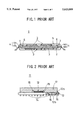
- FIG.1 shows the construction of a typical QFP device 1, wherein the device 1 includes a package substrate 2 carrying thereon a plurality of semiconductor chips 3 on upper and lower major surfaces 2a and 2b.
- the package substrate 2 may be formed of a ceramic, and is encapsulated in a flat resin package body 5, wherein a number of interconnection leads 4 are provided at the peripheral edge of the package body 5.
- Each of the interconnection leads 4 is formed of an inner lead part 4a held within the resin package body 5 and an outer lead part 4b projecting outside the package body 5.
- the inner lead part 4a is connected to a conductor pattern 6 provided on the package substrate 2 by means of a bonding wire 7.
- the bonding wire 7 is also encapsulated in the resin package body 5.
- the outer lead part 4b of the interconnection lead 4 is bent in the downward direction in the vicinity of the peripheral edge of the package body 5 to form a gull wing structure, wherein there is formed a part laterally bent at the distal end of the outer lead part 4b for contacting with a wiring pattern provided on a printed circuit board.
- the QFP device of FIG.1 is suitable for mounting using the art of SMT (surface mounting technology).
- the semiconductor device 1 it is possible to mount the semiconductor chips 3 on both the upper and lower major surfaces of the package substrate 2 as already noted.
- the device 1 is advantageous for increasing the density of mounting of the chips on a package substrate.
- such a construction of increased number of chips on a single chip substrate raises a problem in that the number of the leads 4 extending from the resin package body 5 increases significantly. With such an increase in the number of the leads 4, the pitch between the leads 4 has to be correspondingly reduced. Further, each lead has to have a reduced width. Thereby, the leads 4 become fragile and easily cause a short circuit when the device 1 is mounted upon a printed circuit board. In addition, high precision is required when mounting such a high density semiconductor device upon a printed circuit board.
- FIG. 2 shows the construction of a conventional BGA device 11 that overcomes the foregoing problem of QFP device, wherein the illustrated device 11 has a plastic package body as will be described later.
- the BGA device 11 includes a printed circuit board 12 of a multiple layer structure, wherein the printed circuit board 12 has an upper major surface 12a on which a single semiconductor chip 13 is mounted by a die bonding process, and the like. Further, the printed circuit board 12 has a lower major surface 12b on which a plurality of solder bumps 14 are formed for external connection. Corresponding to each of the solder bumps 14, there is provided a through hole 16 in the printed circuit board 12, wherein the through holes 16 are connected to a wiring pattern (not shown) provided on the upper major surface 12a of the printed circuit board 12.
- the printed circuit board 12 having a multiple layer construction as noted before, may include a plurality of such wiring patterns in a plurality of layers, each in electrical connection with a through hole 16.
- the wiring pattern or patterns on the surface 12a of the printed circuit board 12 are connected to the semiconductor chip 13 by way of bonding wires 15.
- the semiconductor chip 13, the bonding wires 15 and the wiring patterns are encapsulated in a resin package body 17.
- the BGA device 11 of FIG. 2 an increase in the number of external connections is easily accomplished by increasing the number of the solder bumps 14 that may be provided on the entire bottom surface 12b of the printed circuit board 12, without reducing the pitch between the solder bumps 14.
- the BGA device 11 has a disadvantage in that the side of the printed circuit board 12 that can carry the semiconductor chip 13 is limited to the surface 12a. It has not been possible to provide the semiconductor chip 13 on both the upper and lower major surfaces 12a and 12b of the printed circuit board 12.
- Another and more specific object of the present invention is to provide a semiconductor device having a package structure suitable for increasing the number of semiconductor chips mounted upon a common package substrate, without excessively reducing the pitch of the leads used for external connection.
- Another object of the present invention is to provide a semiconductor device, comprising:
- first substrate having upper and lower major surfaces, said first substrate carrying said semiconductor chips on both of said upper and lower major surfaces;
- said second substrate defining a space such that said semiconductor chip provided on said lower major surface of said first substrate is accommodated in said space.
- the present invention it is possible to mount a number of semiconductor chips on a package substrate while using the BGA package structure.
- the present invention can easily attend to the necessary increase in the number of leads even when the number of the semiconductor chips in the package is increased.
- the power conductor pattern on the foregoing support surface is electrically connected to one or more of the solder bumps via a conductor pattern or via-hole that penetrates through the second substrate.
- a support surface is generally formed so as to surround the space mentioned before, the power conductor pattern can have a very large surface area suitable for carrying large electric power for driving a number of semiconductor chips provided on the first substrate.
- the electrical interconnection for supplying electric power from the second substrate to the first substrate is achieved easily by providing a conductive adhesive such as a silver paste, such that the conductive adhesive connects the power conductor pattern on the support surface to a corresponding power conductor pattern provided on the lower major surface of the first substrate.
- the power conductor pattern thereby forms a part of the first interconnection means.
- the first substrate is fixed firmly upon the second substrate by the conductive adhesive.
- the conductor patterns on the upper major surface of the substrate, provided as a part of the first interconnection means for carrying signals, are easily connected to corresponding conductor patterns provided on the second substrate as the second interconnection means, by means of wire bonding process, as the number of the electrode pads on the upper major surface of the first substrate is reduced to about one-half due to the provision of the power electrode pads and the ground pads solely on the lower major surface of the first substrate.
- FIG. 1 is a diagram showing the construction of a conventional semiconductor device having the QFP structure
- FIG. 2 is a diagram showing the construction of a conventional semiconductor device having the BGA structure
- FIG. 3 is a diagram showing the construction of a semiconductor device according to a first embodiment of the present invention.
- FIG. 4 is a diagram showing the semiconductor device of FIG. 3 in an enlarged scale
- FIG. 5 is a diagram showing a modification of the semiconductor device of FIG. 3;
- FIG. 6 is a diagram showing another modification of the device of FIG. 3;
- FIG. 7 is a diagram showing a further modification of the device of FIG. 3;
- FIG. 8 is a diagram showing the construction of a semiconductor device according to a second embodiment of the present invention.
- FIG. 9 is a diagram showing a modification of the semiconductor device of FIG. 8.
- FIGS. 3 and 4 show a semiconductor device 20 according to a first embodiment of the present invention, wherein FIG. 3 shows the semiconductor device 20 in an elevational cross sectional view while FIG. 4 shows a part of the semiconductor device 20 in an enlarged scale.
- the semiconductor device 20 includes a first substrate 21 referred to hereinafter as “intermediate substrate” and a second substrate 22 referred to hereinafter as “mount substrate,” wherein the mount substrate 22 carries thereon the aforementioned intermediate substrate 21.
- the intermediate substrate 21, in turn, carries a plurality of semiconductor chips 23 on both of upper and lower major surfaces 21a and 21b thereof, while the mount substrate 22 carries, on a lower major surface 22b thereof, a plurality of solder bumps 25 that form a BGA structure.
- the intermediate substrate 21 may be formed of a multi-layer ceramic board, and carries, on the upper and lower major surfaces 21a and 22b as well as on an internal layer provided inside the substrate 21, wiring patterns (not illustrated) in a state that the wiring patterns are connected to the semiconductor chips 23 on the substrate 21. Further, the wiring patterns are connected, on the substrate 21, with each other by interconnection patterns 26 embedded in the substrate 21 including via holes. See FIG. 4
- the intermediate substrate 21 carries, on the upper and lower major surfaces 21a and 21b thereof, a number of terminal pads 27 and 28, such that the terminal pads 27 and 28 are disposed, respectively on the upper and lower major surfaces 21a and 21b, along an outer periphery of the substrate 21, wherein each of the terminal pads 27 and 28 are connected to one or more of the semiconductor chips 23, via the wiring patterns provided on the upper and lower major surfaces 21a and 21b of the substrate 21 as well as via the via-holes 26 penetrating through the substrate 21.
- the foregoing terminal pads 27 and 28 generally include signal terminal pads for carrying signals, power terminal pads for carrying electric power, and ground terminal pads used for connection to the ground. Generally, about 60% of the total terminal pads in an integrated circuit are used for the signal terminal pad, while about 40% are used either for the power terminal pad or for the ground pad.
- most or all of the power terminal pads and the ground pads are provided on the lower major surface 21b of the substrate 21 in the form of the terminal pads 28 as indicated in FIG. 4. Further, most or all of the signal terminal pads are provided on the upper major surface 21a in the form of the terminal pads 27.
- the terminal pads 27 on the upper major surface 21a of the intermediate substrate 21 are connected to respective, corresponding signal electrodes 31 that are provided on an upper major surface 22a of the mount substrate 22, by bonding wires 35.
- the mount substrate 22 is typically formed of a multiple-layer printed circuit board of an insulating material such as a BT resin, and the solder bumps 25 on the lower major surface 22b as already noted.
- the solder bumps 25 are connected, in the mount substrate 22, to the corresponding signal electrode pads 31 on the upper major surface 21a by respective via-holes 34 that penetrate through the substrate 22 from the upper major surface 22a to the lower major surface 22b.
- the mount substrate 22 forms a frame structure defined by an inner peripheral wall 22c, wherein the inner peripheral wall 22c defines a central space region 29 at the central part of the frame structure.
- the central space region 29 may be formed by a milling process, while the mount substrate 22 is further formed with a support surface 30 extending along the inner peripheral wall 22c as a recessed upper major surface.
- the support surface 30 supports thereon the intermediate substrate 21.
- the support surface 30 carries thereon an electrode pad 32 connected to one of the solder bumps 25 via a corresponding via-hole 34, and the power terminal pad 28 on the lower major surface 21b of the intermediate substrate 21 is connected to the corresponding electrode pad 32 on the support substrate 30 by means of a bonding layer 33 of a conductive resin such as silver paste, upon mounting of the intermediate substrate 21 on the mount substrate 22.
- the intermediate substrate 21 is held upon the mount substrate 22 firmly by the conductive resin layer 33 with the electric connection that supplied electric power.
- the semiconductor chips 23 on the upper major surface 21a of the intermediate substrate 21 as well as any terminal pads 27 and wires 35 are encapsulated in a resin package body 24a that forms an upper-half part of a resin package body 24 shown in FIG. 3.
- a similar resin package body 24b is provided on the lower major surface 21b of the substrate 21 as a lower-half part of the resin package body 24, such that the resin package body 24b fills the space region 29 and encapsulates the semiconductor chips 23 on the lower major surface 21b as well as the electrode terminals 28 thereon.
- the semiconductor chips 23 mounted upon the lower major surface 21b of the intermediate substrate 21 are accommodated in the space region 29 in the state where the top surface of the semiconductor chips 23 which is the surface opposite the surface of the chip 23 contacting to the lower major surface 21b, is located closer to the lower major surface 21b with respect to the lower major surface 22b of the mount substrate 22b. Thereby, the semiconductor chips 23 on the lower major surface 21b do not become an obstacle in the SMT process of the semiconductor device 20 on a printed circuit board.
- the solder bumps 25 on the lower major surface 22b of the mount substrate 22 form a BGA structure.
- the semiconductor device 20 facilitates the efficiency of mounting process substantially.
- the semiconductor device 20 having such a BGA structure is suitable for efficient surface mounting according to the SMT process.
- the resin package body 24 In fabricating the semiconductor device 20, it is preferable to form the resin package body 24 by a transfer molding process of a thermoplastic resin.
- the semiconductor chips 23 are provided on both the upper and lower major surfaces 21a and 21b of the intermediate substrate 21, the stress applied to the semiconductor chips 23 at the time of molding is equilibrated in the upper major surface 21a and in the lower major surface 21b. Thereby, a problem such a developing of cracks in the resin package body is successfully minimized, and the semiconductor device 20 has a preferable feature of improved reliability.
- Such a molding of the resin package body 24 is of course conducted after the intermediate substrate 21 is mounted upon the mount substrate 22.
- FIG. 5 shows the construction of a semiconductor device 40 as a modification of the semiconductor device 20.
- those parts described previously are designated by the same reference numerals and the description thereof will be omitted.
- the semiconductor device 40 includes a resin package body 41 formed of potting rather than transfer molding.
- the semiconductor device 40 uses a dam 42 on the upper major surface 22a of the mount substrate 22 such that the dam 42 surrounds laterally the area where an upper-half part of the resin package body 41 is to be formed.
- the upper-half part of the resin package body 41 is successfully formed on the upper major surface 21a of the mount substrate 21.
- a resin region is formed to fill the space region 29, defined by the inner peripheral wall 22c of the mount substrate 22, as a lower-half part of the resin package body 41.
- the inner peripheral wall 22c acts as the stopper of the molten resin.
- the potting for the formation of the resin package body, it is possible to eliminate the mold used in the transfer molding process. Thereby, the fabrication cost of the device is reduced. In the present embodiment, too, the problem of cracking of the resin package body 41 is minimized by providing the resin package body on the both sides of the intermediate substrate 21. Further, application of stress to the semiconductor chips 23 is substantially reduced.
- the fixing of the intermediate substrate 21 upon the support surface 30 of the mount substrate 22 is by no means limited to the conductive bonding layer 33 shown in FIG. 4. Instead, one may provide a solder bump in place of the terminal pad 28 and carry out a face-down mounting such that the solder bump fused upon the electrode pad 32 provided on the support surface 30. Further, electrical connection between the terminal pad 28 and the electrode pad 32 may be achieved also by wire bonding. Further, any of ceramic substrate and multiple-layer printed circuit board may be used for the substrates 21 and 22. Further, it is also possible to provide the power and ground terminals on the upper major surface of the substrate 21 and the signal terminals on the lower major surface of the substrate 21.
- FIGS. 6 and 7 show various modifications of the first embodiment of the present invention, wherein those parts described previously are designated by the same reference numerals and the description thereof will be omitted.
- solder bumps 25 are replaced by electrode pins 25' that extend downwardly from the lower major surface of the mount substrate 22.
- the modification of FIG. 7 replaces the solder bumps 25 by electrode lands 25". In any of these embodiments, the desirable effect of the present invention is achieved.
- FIG. 8 shows a second embodiment of the present invention, wherein a single semiconductor chip 41 is mounted upon an intermediate substrate 42 by means of bonding wires 46 or tape lead not illustrated, wherein the intermediate substrate 42 is mounted upon a mount substrate 43 by means of solder bumps 45.
- the mount substrate 43 in turn carries an array of solder bumps 44 on the lower major surface thereof for connection to a printed circuit board and further a resin package body 47 on an upper major surface thereof such that the resin package body 47 covers the semiconductor chip 41 and the intermediate substrate 42.
- a low viscosity resin is introduced into the gap between the intermediate substrate 43 and the mount substrate 43 from an opening 43a provided on the mount substrate 43 to form a second resin body 48.
- FIG. 9 shows a modification of the device of FIG. 8, wherein the semiconductor chip 41 is now provided on the lower major surface of the intermediate substrate 42. Thereby, the semiconductor chip 41 is accommodated in a space defined by the opening 43a of the mount substrate 43. By constructing the semiconductor device as such, it is possible to reduce the height or thickness of the device.
- the interconnection between the semiconductor chip 41 and the intermediate substrate 42 is achieved by a tape lead 46'.
Abstract
Description
Claims (14)
Applications Claiming Priority (2)
| Application Number | Priority Date | Filing Date | Title |
|---|---|---|---|
| JP6-174598 | 1994-07-26 | ||
| JP6174598A JPH0846136A (en) | 1994-07-26 | 1994-07-26 | Semiconductor device |
Publications (1)
| Publication Number | Publication Date |
|---|---|
| US5615089A true US5615089A (en) | 1997-03-25 |
Family
ID=15981375
Family Applications (1)
| Application Number | Title | Priority Date | Filing Date |
|---|---|---|---|
| US08/505,888 Expired - Lifetime US5615089A (en) | 1994-07-26 | 1995-07-24 | BGA semiconductor device including a plurality of semiconductor chips located on upper and lower surfaces of a first substrate |
Country Status (2)
| Country | Link |
|---|---|
| US (1) | US5615089A (en) |
| JP (1) | JPH0846136A (en) |
Cited By (50)
| Publication number | Priority date | Publication date | Assignee | Title |
|---|---|---|---|---|
| WO1998018303A1 (en) * | 1996-10-21 | 1998-04-30 | Alpine Microsystems, Llc | A system and method for packaging integrated circuits |
| US5774340A (en) * | 1996-08-28 | 1998-06-30 | International Business Machines Corporation | Planar redistribution structure and printed wiring device |
| US5790384A (en) * | 1997-06-26 | 1998-08-04 | International Business Machines Corporation | Bare die multiple dies for direct attach |
| US6028364A (en) * | 1994-09-20 | 2000-02-22 | Hitachi, Ltd. | Semiconductor device having a stress relieving mechanism |
| US6038122A (en) * | 1997-08-22 | 2000-03-14 | Telefonaktiebolaget Lm Ericsson | Decoupling capacitor |
| US6038135A (en) * | 1995-06-30 | 2000-03-14 | Fujitsu Limited | Wiring board and semiconductor device |
| US6043559A (en) * | 1996-09-09 | 2000-03-28 | Intel Corporation | Integrated circuit package which contains two in plane voltage busses and a wrap around conductive strip that connects a bond finger to one of the busses |
| US6049467A (en) * | 1998-08-31 | 2000-04-11 | Unisys Corporation | Stackable high density RAM modules |
| US6065980A (en) * | 1998-06-29 | 2000-05-23 | Cisco Technology, Inc. | Grounding a PCB to an enclosure sub-assembly using a grounding spring |
| US6081429A (en) * | 1999-01-20 | 2000-06-27 | Micron Technology, Inc. | Test interposer for use with ball grid array packages assemblies and ball grid array packages including same and methods |
| US6101100A (en) * | 1996-07-23 | 2000-08-08 | International Business Machines Corporation | Multi-electronic device package |
| US6118184A (en) * | 1997-07-18 | 2000-09-12 | Sharp Kabushiki Kaisha | Semiconductor device sealed with a sealing resin and including structure to balance sealing resin flow |
| US6117382A (en) * | 1998-02-05 | 2000-09-12 | Micron Technology, Inc. | Method for encasing array packages |
| US6154371A (en) * | 1998-09-30 | 2000-11-28 | Cisco Technology, Inc. | Printed circuit board assembly and method |
| US6219254B1 (en) * | 1999-04-05 | 2001-04-17 | Trw Inc. | Chip-to-board connection assembly and method therefor |
| US6255899B1 (en) | 1999-09-01 | 2001-07-03 | International Business Machines Corporation | Method and apparatus for increasing interchip communications rates |
| US6282100B1 (en) * | 1999-07-01 | 2001-08-28 | Agere Systems Guardian Corp. | Low cost ball grid array package |
| US6325552B1 (en) | 2000-02-14 | 2001-12-04 | Cisco Technology, Inc. | Solderless optical transceiver interconnect |
| US6329713B1 (en) * | 1998-10-21 | 2001-12-11 | International Business Machines Corporation | Integrated circuit chip carrier assembly comprising a stiffener attached to a dielectric substrate |
| US6329686B1 (en) | 1999-11-12 | 2001-12-11 | Micron Technology, Inc. | Method of fabricating conductive straps to interconnect contacts to corresponding digit lines by employing an angled sidewall implant and semiconductor devices fabricated thereby |
| KR100326822B1 (en) * | 1998-04-30 | 2002-03-04 | 가네꼬 히사시 | Semiconductor device with reduced thickness and manufacturing method thereof |
| US6400576B1 (en) * | 1999-04-05 | 2002-06-04 | Sun Microsystems, Inc. | Sub-package bypass capacitor mounting for an array packaged integrated circuit |
| US20020076854A1 (en) * | 2000-12-15 | 2002-06-20 | Pierce John L. | System, method and apparatus for constructing a semiconductor wafer-interposer using B-Stage laminates |
| US20020078401A1 (en) * | 2000-12-15 | 2002-06-20 | Fry Michael Andrew | Test coverage analysis system |
| US6423571B2 (en) | 1994-09-20 | 2002-07-23 | Hitachi, Ltd. | Method of making a semiconductor device having a stress relieving mechanism |
| US20020097063A1 (en) * | 1999-11-16 | 2002-07-25 | Kline Jerry D. | Wafer level interposer |
| US20020119600A1 (en) * | 2001-02-23 | 2002-08-29 | Micro-Asi, Inc. | Wafer-interposer using a ceramic substrate |
| US6475830B1 (en) | 2000-07-19 | 2002-11-05 | Cisco Technology, Inc. | Flip chip and packaged memory module |
| US6512303B2 (en) | 1995-12-19 | 2003-01-28 | Micron Technology, Inc. | Flip chip adaptor package for bare die |
| US20030128044A1 (en) * | 2000-12-15 | 2003-07-10 | Pierce John L. | Method for producing a wafer interposer for use in a wafer interposer assembly |
| US20030129775A1 (en) * | 2000-07-31 | 2003-07-10 | Kline Jerry D. | Matched set of integrated circuit chips selected from a multi wafer interposer |
| US6592269B1 (en) * | 2001-08-31 | 2003-07-15 | Cypress Semiconductor Corporation | Apparatus and method for integrating an optical transceiver with a surface mount package |
| US20030148108A1 (en) * | 2000-12-15 | 2003-08-07 | Pierce John L. | Wafer interposer assembly and system for building same |
| US6630737B2 (en) * | 1999-06-10 | 2003-10-07 | Koninklijke Philips Electronics N.V. | Integrated circuit package, ball-grid array integrated circuit package |
| US20040000707A1 (en) * | 2001-10-26 | 2004-01-01 | Staktek Group, L.P. | Modularized die stacking system and method |
| US6686657B1 (en) | 2000-11-07 | 2004-02-03 | Eaglestone Partners I, Llc | Interposer for improved handling of semiconductor wafers and method of use of same |
| US20040100778A1 (en) * | 2002-11-25 | 2004-05-27 | Patrizio Vinciarelli | Power converter package and thermal management |
| EP1429389A1 (en) * | 2002-12-12 | 2004-06-16 | Alps Electric Co., Ltd. | Compact circuit module having high mounting accuracy and method of manufacturing the same |
| US20040113281A1 (en) * | 2002-12-17 | 2004-06-17 | Brandenburg Scott D. | Multi-chip module and method of forming |
| US6759316B2 (en) * | 1998-08-18 | 2004-07-06 | Oki Electric Industry Co., Ltd. | Method of manufacturing a semiconductor chip |
| US20040155328A1 (en) * | 2000-07-31 | 2004-08-12 | Kline Jerry D. | Wafer-interposer assembly |
| US6815712B1 (en) | 2000-10-02 | 2004-11-09 | Eaglestone Partners I, Llc | Method for selecting components for a matched set from a wafer-interposer assembly |
| US6861290B1 (en) * | 1995-12-19 | 2005-03-01 | Micron Technology, Inc. | Flip-chip adaptor package for bare die |
| US20050231922A1 (en) * | 2004-04-16 | 2005-10-20 | Jung-Chien Chang | Functional printed circuit board module with an embedded chip |
| US6963142B2 (en) * | 2001-10-26 | 2005-11-08 | Micron Technology, Inc. | Flip chip integrated package mount support |
| US20060091543A1 (en) * | 2004-10-28 | 2006-05-04 | Samsung Electronics Co.; Ltd | Land grid array module |
| US20080284066A1 (en) * | 2007-05-16 | 2008-11-20 | Heap Hoe Kuan | Integrated circuit package system employing resilient member mold system technology |
| US20100314730A1 (en) * | 2009-06-16 | 2010-12-16 | Broadcom Corporation | Stacked hybrid interposer through silicon via (TSV) package |
| USRE43112E1 (en) | 1998-05-04 | 2012-01-17 | Round Rock Research, Llc | Stackable ball grid array package |
| US8772916B2 (en) | 2006-12-22 | 2014-07-08 | Stats Chippac Ltd. | Integrated circuit package system employing mold flash prevention technology |
Families Citing this family (1)
| Publication number | Priority date | Publication date | Assignee | Title |
|---|---|---|---|---|
| DE102007007503A1 (en) * | 2007-02-15 | 2008-08-21 | Robert Bosch Gmbh | component assembly |
Citations (9)
| Publication number | Priority date | Publication date | Assignee | Title |
|---|---|---|---|---|
| JPS60117763A (en) * | 1983-11-30 | 1985-06-25 | Fujitsu Ltd | Semiconductor device |
| US5060844A (en) * | 1990-07-18 | 1991-10-29 | International Business Machines Corporation | Interconnection structure and test method |
| JPH04219966A (en) * | 1990-12-20 | 1992-08-11 | Fujitsu Ltd | Semiconductor element |
| JPH0548000A (en) * | 1991-08-13 | 1993-02-26 | Fujitsu Ltd | Semiconductor device |
| US5216278A (en) * | 1990-12-04 | 1993-06-01 | Motorola, Inc. | Semiconductor device having a pad array carrier package |
| US5241133A (en) * | 1990-12-21 | 1993-08-31 | Motorola, Inc. | Leadless pad array chip carrier |
| JPH0629422A (en) * | 1992-07-13 | 1994-02-04 | Nec Corp | Hybrid integrated circuit device |
| US5473190A (en) * | 1993-12-14 | 1995-12-05 | Intel Corporation | Tab tape |
| US5519176A (en) * | 1993-04-05 | 1996-05-21 | Sony Corporation | Substrate and ceramic package |
-
1994
- 1994-07-26 JP JP6174598A patent/JPH0846136A/en not_active Withdrawn
-
1995
- 1995-07-24 US US08/505,888 patent/US5615089A/en not_active Expired - Lifetime
Patent Citations (10)
| Publication number | Priority date | Publication date | Assignee | Title |
|---|---|---|---|---|
| JPS60117763A (en) * | 1983-11-30 | 1985-06-25 | Fujitsu Ltd | Semiconductor device |
| US5060844A (en) * | 1990-07-18 | 1991-10-29 | International Business Machines Corporation | Interconnection structure and test method |
| US5216278A (en) * | 1990-12-04 | 1993-06-01 | Motorola, Inc. | Semiconductor device having a pad array carrier package |
| JPH04219966A (en) * | 1990-12-20 | 1992-08-11 | Fujitsu Ltd | Semiconductor element |
| US5241133A (en) * | 1990-12-21 | 1993-08-31 | Motorola, Inc. | Leadless pad array chip carrier |
| JPH0548000A (en) * | 1991-08-13 | 1993-02-26 | Fujitsu Ltd | Semiconductor device |
| US5297006A (en) * | 1991-08-13 | 1994-03-22 | Fujitsu Limited | Three-dimensional multi-chip module |
| JPH0629422A (en) * | 1992-07-13 | 1994-02-04 | Nec Corp | Hybrid integrated circuit device |
| US5519176A (en) * | 1993-04-05 | 1996-05-21 | Sony Corporation | Substrate and ceramic package |
| US5473190A (en) * | 1993-12-14 | 1995-12-05 | Intel Corporation | Tab tape |
Cited By (95)
| Publication number | Priority date | Publication date | Assignee | Title |
|---|---|---|---|---|
| US6028364A (en) * | 1994-09-20 | 2000-02-22 | Hitachi, Ltd. | Semiconductor device having a stress relieving mechanism |
| US6423571B2 (en) | 1994-09-20 | 2002-07-23 | Hitachi, Ltd. | Method of making a semiconductor device having a stress relieving mechanism |
| US6038135A (en) * | 1995-06-30 | 2000-03-14 | Fujitsu Limited | Wiring board and semiconductor device |
| US20060211174A1 (en) * | 1995-12-19 | 2006-09-21 | Moden Walter L | Flip-chip adaptor package for bare die |
| US20100155930A1 (en) * | 1995-12-19 | 2010-06-24 | Micron Technology, Inc. | Stackable semiconductor device assemblies |
| US8049317B2 (en) | 1995-12-19 | 2011-11-01 | Round Rock Research, Llc | Grid array packages |
| US20050167850A1 (en) * | 1995-12-19 | 2005-08-04 | Moden Walter L. | Flip-chip adaptor package for bare die |
| US7381591B2 (en) | 1995-12-19 | 2008-06-03 | Micron Technology, Inc. | Flip-chip adaptor package for bare die |
| US20100155966A1 (en) * | 1995-12-19 | 2010-06-24 | Micron Technology, Inc. | Grid array packages |
| US8164175B2 (en) | 1995-12-19 | 2012-04-24 | Round Rock Research, Llc | Stackable semiconductor device assemblies |
| US8299598B2 (en) | 1995-12-19 | 2012-10-30 | Round Rock Research, Llc | Grid array packages and assemblies including the same |
| US6667556B2 (en) | 1995-12-19 | 2003-12-23 | Micron Technology, Inc. | Flip chip adaptor package for bare die |
| US20100148352A1 (en) * | 1995-12-19 | 2010-06-17 | Micron Technology, Inc. | Grid array packages and assemblies including the same |
| US8198138B2 (en) | 1995-12-19 | 2012-06-12 | Round Rock Research, Llc | Methods for providing and using grid array packages |
| US7329945B2 (en) | 1995-12-19 | 2008-02-12 | Micron Technology, Inc. | Flip-chip adaptor package for bare die |
| US6512303B2 (en) | 1995-12-19 | 2003-01-28 | Micron Technology, Inc. | Flip chip adaptor package for bare die |
| US6861290B1 (en) * | 1995-12-19 | 2005-03-01 | Micron Technology, Inc. | Flip-chip adaptor package for bare die |
| US6101100A (en) * | 1996-07-23 | 2000-08-08 | International Business Machines Corporation | Multi-electronic device package |
| US6000130A (en) * | 1996-08-28 | 1999-12-14 | International Business Machines Corporation | Process for making planar redistribution structure |
| US5774340A (en) * | 1996-08-28 | 1998-06-30 | International Business Machines Corporation | Planar redistribution structure and printed wiring device |
| US6440770B1 (en) | 1996-09-09 | 2002-08-27 | Intel Corporation | Integrated circuit package |
| US6043559A (en) * | 1996-09-09 | 2000-03-28 | Intel Corporation | Integrated circuit package which contains two in plane voltage busses and a wrap around conductive strip that connects a bond finger to one of the busses |
| US6075711A (en) * | 1996-10-21 | 2000-06-13 | Alpine Microsystems, Inc. | System and method for routing connections of integrated circuits |
| WO1998018303A1 (en) * | 1996-10-21 | 1998-04-30 | Alpine Microsystems, Llc | A system and method for packaging integrated circuits |
| US5790384A (en) * | 1997-06-26 | 1998-08-04 | International Business Machines Corporation | Bare die multiple dies for direct attach |
| US6118184A (en) * | 1997-07-18 | 2000-09-12 | Sharp Kabushiki Kaisha | Semiconductor device sealed with a sealing resin and including structure to balance sealing resin flow |
| US6038122A (en) * | 1997-08-22 | 2000-03-14 | Telefonaktiebolaget Lm Ericsson | Decoupling capacitor |
| US6616880B2 (en) | 1998-02-05 | 2003-09-09 | Micron Technology, Inc. | Method for encasing array packages |
| US6332766B1 (en) | 1998-02-05 | 2001-12-25 | Micron Technology, Inc. | Apparatus for encasing array packages |
| US6893244B2 (en) | 1998-02-05 | 2005-05-17 | Micron Technology, Inc. | Apparatus for encasing array packages |
| US20040033283A1 (en) * | 1998-02-05 | 2004-02-19 | Thummel Steven G. | Apparatus for encasing array packages |
| US6989121B2 (en) | 1998-02-05 | 2006-01-24 | Micron Technology, Inc. | Method for encasing plastic array packages |
| US6287503B1 (en) | 1998-02-05 | 2001-09-11 | Micron Technology, Inc. | Method for encasing array packages |
| US20040026823A1 (en) * | 1998-02-05 | 2004-02-12 | Thummel Steven G. | Method for encasing plastic array packages |
| US6626656B2 (en) | 1998-02-05 | 2003-09-30 | Micron Technology, Inc. | Apparatus for encasing array packages |
| US6117382A (en) * | 1998-02-05 | 2000-09-12 | Micron Technology, Inc. | Method for encasing array packages |
| KR100326822B1 (en) * | 1998-04-30 | 2002-03-04 | 가네꼬 히사시 | Semiconductor device with reduced thickness and manufacturing method thereof |
| USRE43112E1 (en) | 1998-05-04 | 2012-01-17 | Round Rock Research, Llc | Stackable ball grid array package |
| US6065980A (en) * | 1998-06-29 | 2000-05-23 | Cisco Technology, Inc. | Grounding a PCB to an enclosure sub-assembly using a grounding spring |
| US6759316B2 (en) * | 1998-08-18 | 2004-07-06 | Oki Electric Industry Co., Ltd. | Method of manufacturing a semiconductor chip |
| US6049467A (en) * | 1998-08-31 | 2000-04-11 | Unisys Corporation | Stackable high density RAM modules |
| US6154371A (en) * | 1998-09-30 | 2000-11-28 | Cisco Technology, Inc. | Printed circuit board assembly and method |
| US6329713B1 (en) * | 1998-10-21 | 2001-12-11 | International Business Machines Corporation | Integrated circuit chip carrier assembly comprising a stiffener attached to a dielectric substrate |
| US6081429A (en) * | 1999-01-20 | 2000-06-27 | Micron Technology, Inc. | Test interposer for use with ball grid array packages assemblies and ball grid array packages including same and methods |
| US6452807B1 (en) * | 1999-01-20 | 2002-09-17 | Micron Technology, Inc. | Test interposer for use with ball grid array packages, assemblies and ball grid array packages including same, and methods |
| US6400576B1 (en) * | 1999-04-05 | 2002-06-04 | Sun Microsystems, Inc. | Sub-package bypass capacitor mounting for an array packaged integrated circuit |
| US6219254B1 (en) * | 1999-04-05 | 2001-04-17 | Trw Inc. | Chip-to-board connection assembly and method therefor |
| USRE42332E1 (en) * | 1999-06-10 | 2011-05-10 | Taiwan Semiconductor Manufacturing Company, Ltd. | Integrated circuit package, ball-grid array integrated circuit package |
| USRE42457E1 (en) | 1999-06-10 | 2011-06-14 | Taiwan Semiconductor Manufacturing Company, Ltd. | Methods of packaging an integrated circuit and methods of forming an integrated circuit package |
| US6630737B2 (en) * | 1999-06-10 | 2003-10-07 | Koninklijke Philips Electronics N.V. | Integrated circuit package, ball-grid array integrated circuit package |
| US6282100B1 (en) * | 1999-07-01 | 2001-08-28 | Agere Systems Guardian Corp. | Low cost ball grid array package |
| US6255899B1 (en) | 1999-09-01 | 2001-07-03 | International Business Machines Corporation | Method and apparatus for increasing interchip communications rates |
| US6329686B1 (en) | 1999-11-12 | 2001-12-11 | Micron Technology, Inc. | Method of fabricating conductive straps to interconnect contacts to corresponding digit lines by employing an angled sidewall implant and semiconductor devices fabricated thereby |
| US6600191B2 (en) | 1999-11-12 | 2003-07-29 | Micron Technology, Inc. | Method of fabricating conductive straps to interconnect contacts to corresponding digit lines by employing an angled sidewall implant and semiconductor devices fabricated thereby |
| US6426528B2 (en) | 1999-11-12 | 2002-07-30 | Micron Technology, Inc. | Method of fabricating conductive straps to interconnect contacts to corresponding digit lines by employing an angled sidewall implant and semiconductor devices fabricated thereby |
| US20020097063A1 (en) * | 1999-11-16 | 2002-07-25 | Kline Jerry D. | Wafer level interposer |
| US6825678B2 (en) | 1999-11-16 | 2004-11-30 | Eaglestone Partners I, Llc | Wafer level interposer |
| US6325552B1 (en) | 2000-02-14 | 2001-12-04 | Cisco Technology, Inc. | Solderless optical transceiver interconnect |
| US6475830B1 (en) | 2000-07-19 | 2002-11-05 | Cisco Technology, Inc. | Flip chip and packaged memory module |
| US6812048B1 (en) | 2000-07-31 | 2004-11-02 | Eaglestone Partners I, Llc | Method for manufacturing a wafer-interposer assembly |
| US20040155328A1 (en) * | 2000-07-31 | 2004-08-12 | Kline Jerry D. | Wafer-interposer assembly |
| US6967494B2 (en) | 2000-07-31 | 2005-11-22 | Eaglestone Partners I, Llc | Wafer-interposer assembly |
| US6759741B2 (en) | 2000-07-31 | 2004-07-06 | Eaglestone Partners I, Llc | Matched set of integrated circuit chips selected from a multi wafer-interposer |
| US20030129775A1 (en) * | 2000-07-31 | 2003-07-10 | Kline Jerry D. | Matched set of integrated circuit chips selected from a multi wafer interposer |
| US6815712B1 (en) | 2000-10-02 | 2004-11-09 | Eaglestone Partners I, Llc | Method for selecting components for a matched set from a wafer-interposer assembly |
| US6927083B2 (en) | 2000-11-07 | 2005-08-09 | Eaglestone Partners I, Llc | Method for constructing a wafer-interposer assembly |
| US6686657B1 (en) | 2000-11-07 | 2004-02-03 | Eaglestone Partners I, Llc | Interposer for improved handling of semiconductor wafers and method of use of same |
| US20040166663A1 (en) * | 2000-11-07 | 2004-08-26 | Kline Jerry D. | Method for constructing a wafer-interposer assembly |
| US6933617B2 (en) | 2000-12-15 | 2005-08-23 | Eaglestone Partners I, Llc | Wafer interposer assembly |
| US20020076854A1 (en) * | 2000-12-15 | 2002-06-20 | Pierce John L. | System, method and apparatus for constructing a semiconductor wafer-interposer using B-Stage laminates |
| US20020078401A1 (en) * | 2000-12-15 | 2002-06-20 | Fry Michael Andrew | Test coverage analysis system |
| US20030128044A1 (en) * | 2000-12-15 | 2003-07-10 | Pierce John L. | Method for producing a wafer interposer for use in a wafer interposer assembly |
| US7036218B2 (en) | 2000-12-15 | 2006-05-02 | Eaglestone Partners I, Llc | Method for producing a wafer interposer for use in a wafer interposer assembly |
| US20030148108A1 (en) * | 2000-12-15 | 2003-08-07 | Pierce John L. | Wafer interposer assembly and system for building same |
| US6673653B2 (en) | 2001-02-23 | 2004-01-06 | Eaglestone Partners I, Llc | Wafer-interposer using a ceramic substrate |
| US20020119600A1 (en) * | 2001-02-23 | 2002-08-29 | Micro-Asi, Inc. | Wafer-interposer using a ceramic substrate |
| US6592269B1 (en) * | 2001-08-31 | 2003-07-15 | Cypress Semiconductor Corporation | Apparatus and method for integrating an optical transceiver with a surface mount package |
| US6963142B2 (en) * | 2001-10-26 | 2005-11-08 | Micron Technology, Inc. | Flip chip integrated package mount support |
| US20040000707A1 (en) * | 2001-10-26 | 2004-01-01 | Staktek Group, L.P. | Modularized die stacking system and method |
| US7799615B2 (en) | 2002-11-25 | 2010-09-21 | Vlt, Inc. | Power converter package and thermal management |
| US7361844B2 (en) * | 2002-11-25 | 2008-04-22 | Vlt, Inc. | Power converter package and thermal management |
| US20080112139A1 (en) * | 2002-11-25 | 2008-05-15 | Vlt, Inc. | Power converter package and thermal management |
| US20040100778A1 (en) * | 2002-11-25 | 2004-05-27 | Patrizio Vinciarelli | Power converter package and thermal management |
| EP1429389A1 (en) * | 2002-12-12 | 2004-06-16 | Alps Electric Co., Ltd. | Compact circuit module having high mounting accuracy and method of manufacturing the same |
| US6833628B2 (en) * | 2002-12-17 | 2004-12-21 | Delphi Technologies, Inc. | Mutli-chip module |
| EP1432033A1 (en) * | 2002-12-17 | 2004-06-23 | Delphi Technologies, Inc. | Multi-chip module and method of forming |
| US20040113281A1 (en) * | 2002-12-17 | 2004-06-17 | Brandenburg Scott D. | Multi-chip module and method of forming |
| US20050093144A1 (en) * | 2002-12-17 | 2005-05-05 | Delphi Technologies, Inc. | Multi-chip module |
| US20050231922A1 (en) * | 2004-04-16 | 2005-10-20 | Jung-Chien Chang | Functional printed circuit board module with an embedded chip |
| US7208824B2 (en) * | 2004-10-28 | 2007-04-24 | Samsung Electronics Co., Ltd. | Land grid array module |
| US20060091543A1 (en) * | 2004-10-28 | 2006-05-04 | Samsung Electronics Co.; Ltd | Land grid array module |
| US8772916B2 (en) | 2006-12-22 | 2014-07-08 | Stats Chippac Ltd. | Integrated circuit package system employing mold flash prevention technology |
| US20080284066A1 (en) * | 2007-05-16 | 2008-11-20 | Heap Hoe Kuan | Integrated circuit package system employing resilient member mold system technology |
| US8852986B2 (en) * | 2007-05-16 | 2014-10-07 | Stats Chippac Ltd. | Integrated circuit package system employing resilient member mold system technology |
| US20100314730A1 (en) * | 2009-06-16 | 2010-12-16 | Broadcom Corporation | Stacked hybrid interposer through silicon via (TSV) package |
Also Published As
| Publication number | Publication date |
|---|---|
| JPH0846136A (en) | 1996-02-16 |
Similar Documents
| Publication | Publication Date | Title |
|---|---|---|
| US5615089A (en) | BGA semiconductor device including a plurality of semiconductor chips located on upper and lower surfaces of a first substrate | |
| US6468834B1 (en) | Method of fabricating a BGA package using PCB and tape in a die-up configuration | |
| US6803254B2 (en) | Wire bonding method for a semiconductor package | |
| US5508556A (en) | Leaded semiconductor device having accessible power supply pad terminals | |
| US6563217B2 (en) | Module assembly for stacked BGA packages | |
| US5854512A (en) | High density leaded ball-grid array package | |
| US5739588A (en) | Semiconductor device | |
| US6201302B1 (en) | Semiconductor package having multi-dies | |
| US6455928B2 (en) | Stackable ball grid array package | |
| US6088233A (en) | Semiconductor device and assembly board having through-holes filled with filling core | |
| US6781242B1 (en) | Thin ball grid array package | |
| JP2000133767A (en) | Laminated semiconductor package and its manufacture | |
| US6448110B1 (en) | Method for fabricating a dual-chip package and package formed | |
| US6340839B1 (en) | Hybrid integrated circuit | |
| JP2001156251A (en) | Semiconductor device | |
| US6819565B2 (en) | Cavity-down ball grid array semiconductor package with heat spreader | |
| US7173341B2 (en) | High performance thermally enhanced package and method of fabricating the same | |
| KR100444170B1 (en) | semiconductor package | |
| KR100456482B1 (en) | Bga package using patterned leadframe to reduce fabricating cost as compared with bga package using substrate having stacked multilayered interconnection pattern layer | |
| KR100247641B1 (en) | Package and method of manufacturing the same | |
| JP2990120B2 (en) | Semiconductor device | |
| KR100473336B1 (en) | semiconductor package | |
| KR100708050B1 (en) | semiconductor package | |
| KR19990056764A (en) | Ball grid array package | |
| KR0161117B1 (en) | Semiconductor package device |
Legal Events
| Date | Code | Title | Description |
|---|---|---|---|
| AS | Assignment |
Owner name: FUJITSU LIMITED, JAPAN Free format text: ASSIGNMENT OF ASSIGNORS INTEREST;ASSIGNORS:YONEDA, YOSHIHIRO;OZAWA, TAKASHI;REEL/FRAME:007599/0733 Effective date: 19950608 |
|
| STCF | Information on status: patent grant |
Free format text: PATENTED CASE |
|
| FEPP | Fee payment procedure |
Free format text: PAYOR NUMBER ASSIGNED (ORIGINAL EVENT CODE: ASPN); ENTITY STATUS OF PATENT OWNER: LARGE ENTITY |
|
| FPAY | Fee payment |
Year of fee payment: 4 |
|
| FPAY | Fee payment |
Year of fee payment: 8 |
|
| FPAY | Fee payment |
Year of fee payment: 12 |
|
| AS | Assignment |
Owner name: FUJITSU MICROELECTRONICS LIMITED, JAPAN Free format text: ASSIGNMENT OF ASSIGNORS INTEREST;ASSIGNOR:FUJITSU LIMITED;REEL/FRAME:021976/0876 Effective date: 20081104 Owner name: FUJITSU MICROELECTRONICS LIMITED,JAPAN Free format text: ASSIGNMENT OF ASSIGNORS INTEREST;ASSIGNOR:FUJITSU LIMITED;REEL/FRAME:021976/0876 Effective date: 20081104 |
|
| AS | Assignment |
Owner name: FUJITSU SEMICONDUCTOR LIMITED, JAPAN Free format text: CHANGE OF NAME;ASSIGNOR:FUJITSU MICROELECTRONICS LIMITED;REEL/FRAME:024804/0269 Effective date: 20100401 |
|
| AS | Assignment |
Owner name: SOCIONEXT INC., JAPAN Free format text: ASSIGNMENT OF ASSIGNORS INTEREST;ASSIGNOR:FUJITSU SEMICONDUCTOR LIMITED;REEL/FRAME:035508/0637 Effective date: 20150302 |