US5625563A - Method and system for reducing the number of connections between a plurality of semiconductor devices - Google Patents
Method and system for reducing the number of connections between a plurality of semiconductor devices Download PDFInfo
- Publication number
- US5625563A US5625563A US08/370,210 US37021095A US5625563A US 5625563 A US5625563 A US 5625563A US 37021095 A US37021095 A US 37021095A US 5625563 A US5625563 A US 5625563A
- Authority
- US
- United States
- Prior art keywords
- signal
- integrated circuit
- semiconductor device
- serial
- high speed
- Prior art date
- Legal status (The legal status is an assumption and is not a legal conclusion. Google has not performed a legal analysis and makes no representation as to the accuracy of the status listed.)
- Expired - Lifetime
Links
Images


Classifications
-
- G—PHYSICS
- G11—INFORMATION STORAGE
- G11C—STATIC STORES
- G11C5/00—Details of stores covered by group G11C11/00
- G11C5/06—Arrangements for interconnecting storage elements electrically, e.g. by wiring
- G11C5/066—Means for reducing external access-lines for a semiconductor memory clip, e.g. by multiplexing at least address and data signals
-
- H—ELECTRICITY
- H04—ELECTRIC COMMUNICATION TECHNIQUE
- H04L—TRANSMISSION OF DIGITAL INFORMATION, e.g. TELEGRAPHIC COMMUNICATION
- H04L12/00—Data switching networks
- H04L12/28—Data switching networks characterised by path configuration, e.g. LAN [Local Area Networks] or WAN [Wide Area Networks]
Definitions
- This invention relates to interconnection of digital integrated circuits and, more particularly, to reducing the number of input/output pins needed for communications and control between a plurality of digital integrated circuits.
- An integrated circuit die may comprise, on a small silicon chip, many thousand or even a million or more transistors interconnected together to form complex electronic functions.
- the complex electronic functions of the integrated circuit chip may require hundreds of external connections to a related electronic system.
- VLSI very large scale integration
- ULSI ultra large scale integration
- IC integrated circuits
- IC packaging industry has therefore developed more sophisticated IC packages to accommodate the increased number of external connections required to be made to the associated electronic system.
- These IC packages are expensive, difficult to fabricate, may require expensive sockets and take up a lot of valuable electronic system circuit board area.
- IC packaging technology has not been able to keep up with the rapidly increasing complexity and sophistication of integrated circuit technologies. This lag in IC packaging technology has limited the ability of the electronic circuit designer to utilize the full capabilities of present and future IC technologies in an easy to implement and cost effective way.
- parallel data signals may be digital words having 32, 64, 128 or more bits, and be connected to a parallel data bus having an equal number of conductive lands or wires such as a computer back plane or the like.
- the close proximity of many parallel signals having to drive a capacitive bus that may not be impedance matched creates signal crosstalk.
- Signal crosstalk further restricts the effective data rate and number of digital devices that may be effectively interconnected in an electronic system.
- semiconductor device refers to a silicon chip or die containing electronic circuitry and is more commonly referred to as a "semiconductor integrated circuit” or “integrated circuit.”
- semiconductor device assembly or “integrated circuit assembly” refers to the silicon die and associated packaging containing the die, including conductive leads, such as ball bump, pins, surface mount gull wing and J leads, conductive tabs or balls at the periphery of a package and/or on the interior of a surface or the like, for connecting to a system circuit board, and internal connections of the die to the conductive leads such as bond wires or tape automated bonding ("TAB").
- TAB tape automated bonding
- semiconductor device assembly or "integrated circuit assembly” may also refer to the silicon die and associated leadframe such as a tape carrier or package-less silicon die on a leadframe which may be encapsulated or not.
- the leadframe is connected to the package-less silicon die as is well known to those skilled in the art of semiconductor devices.
- Yet another object is to implement a digital serial interface in an integrated circuit.
- Still another object is to implement a scalable digital serial interface in a semiconductor integrated circuit.
- Yet another object is to implement a dormant digital serial interface in a semiconductor integrated circuit for activation by a hardware enable signal or software program command.
- a further object is to implement a simple serial interface in a semiconductor integrated circuit.
- Another object is a scalable digital serial interface having reserve data transmission capacity for future increases in the mount of data transferred.
- a semiconductor integrated circuit incorporates a high speed digital serial communications and control interface.
- This serial interface transmits and receives digital information and control signals on a serial digital communications link that may be communicated over, for example, coaxial cable, twisted pair, glass fiber optic light conduit, wireless such as cellular, VHF and UHF radio, microwave or focused infrared.
- the present invention eliminates the need for complex multi-wire digital buses presently needed to interconnect high speed digital information between integrated circuit devices containing the various complex and high speed semiconductor devices.
- the heretofore parallel data buses have created the requirement for high pin count packages in order to transmit in parallel (simultaneous data transmission) the digital information.
- routing of these parallel data buses on the system printed circuit board is difficult and requires a significant amount of circuit board area.
- serial high speed interconnect devices may be implemented from any number of existing technologies that are being presently utilized for sending and receiving high speed digital computer data.
- Typical digital protocols are well known to those skilled in the art of digital communication systems as may be utilized for data modems, local area networks ("LAN”), wide area networks (“WAN”), and the like (both “wired” and “wireless” configurations).
- the Marbot Patents teach a method and system for digital data transmission that also includes a means of creating all necessary clock and synchronization information for the data so as to constitute the transmission signal and determine the transmission speed, clock rate, and synchronization lock from the revived transmission signal.
- the circuits disclosed in the Marbot Patents may be integrated onto the semiconductor device or on another semiconductor device proximate to the IC device in the same semiconductor device assembly.
- Use of serial transmission and reception digital logic circuits requiring no analog phase lock loop subsystems helps make the present invention economically practical.
- a minimum of digital protocol overhead is required and digital communication between the various semiconductor devices is rapid and reliable.
- circuits of the Marbot Patents, and other similar types of circuits, in the present invention is well known to those skilled in the art of digital communications systems and integrated circuit design.
- Integrated circuits utilizing the Marbot Patents or similar technologies are easily designed and preferably may be combined with the other digital circuits on the semiconductor integrated circuit.
- a serial digital transmission technology that may be utilized is SeriaLinkTM (SERIALINK is a trademark of LSI Logic Corporation) circuits.
- SERIALINK is owned by LSI Logic Corporation. This SERIALINK technology is more fully described in "SeriaLink SL300 High-Speed Serializer/Deserializer Technical Manual," LSI Logic Document DB04-000042-00, First Edition.
- SHSID serial high speed interconnect devices
- SCI Scalable Coherent Interface
- ATM Asynchronous Transfer Mode
- Fiber Channel SerialBus
- SCSI SerialBus
- SSA QuickRing
- HIPPI High-speed interconnection technologies
- a feature of the present invention is the simplicity in which the various semiconductor devices may be connected (bused) together.
- the serial link(s) of the present invention multiplex and serially transmit the various digital I/O signals so that a smaller number of interconnections are needed for transmission thereof.
- the multiplexed signals may be serially transmitted at a very high data rate, for example, greater than one GigaHertz. This very high multiplexed data rate has sufficient information bandwidth to handle the majority of computational and data transfer intensive applications presently implemented in digital electronic systems. Where a higher data throughput is desired, the present invention is easily scalable up to the higher data throughput required by utilizing multiple serial links.
- Each serial link is capable of data rates of, for example, greater than one Gigabit per second ("GBS"). It is also a feature of the present invention that the serial link may be run at a slower data rate and "speeded up" for future applications by increasing the data transfer rate of the serial link by hardware and/or software control.
- Physical serial link interconnections between the semiconductor devices may be made with constant impedance strip line, coaxial cable, twisted wire pair or the like.
- the semiconductor devices may be on one substrate or printed circuit beard or on a plurality of printed circuit beards.
- wireless interconnections may be accomplished between the semiconductor devices by using microwave, focused infrared, spread spectrum or other wireless data transmission systems.
- cables, wires, twisted pairs and the like also include non-physical, i.e., wireless connections as is well known to those skilled in the art.
- the wireless communications medium may also be part of the semiconductor device assembly or fabricated onto the semiconductor integrated circuit.
- a feature of the present invention is implementation of at least one high speed serial link in each semiconductor device.
- This serial link may initially remain dormant and not utilized until it is required in the electronic system.
- the electrical designer may choose to interconnect but not utilize the high speed data serial link until required in the system, i.e., future system upgrade or expansion.
- serial link(s) remain dormant until needed allows using ICs in existing parallel bus systems and then being able to easily upgrade system performance by simply enabling the serial link(s) which already exist in the ICs of the present invention.
- existing equipment designs need not be made obsolete.
- new designs utilizing the serial link(s) of the present invention may be integrated into normal product design updates and will be ready for full implementation of the serial link(s) when appropriate. This also facilitates reduction in manufacturing costs by allowing the use of lower cost IC packages and interconnecting these reduced cost IC packages with serial link(s) of the present invention.
- the selection, combination and interplay between the semiconductor devices and their relative locations is greatly expanded because, with the present invention, the designer is not required to rely on a plurality of individual signal wires in a parallel bus configuration that has to be correctly interconnected between the semiconductor devices.
- the semiconductor devices no longer must be in close proximity to one another on the same system printed circuit board, or closely coupled system and daughter boards.
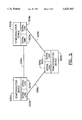
- FIG. 1 is a schematic block diagram of a prior art interconnection of two integrated circuit assemblies
- FIG. 2 is a schematic block diagram of a preferred embodiment of the present invention.
- FIG. 3 is a schematic block diagram of an embodiment of the present invention having a plurality of serial high speed interconnect devices
- FIG. 4 is a schematic block diagram of the present invention interconnected in a star configuration
- FIG. 5 is a schematic block diagram of the present invention interconnected in a ring configuration
- FIG. 6 is a schematic block diagram of a fiber optic interconnection of the present invention.
- FIG. 7 is a schematic block diagram of an infrared interconnection of the present invention.
- FIG. 8 is a schematic block diagram of a radio frequency spread spectrum interconnection of the present invention.
- FIG. 1 illustrates two integrated circuit assemblies connected together by a parallel bus comprising a plurality of wires, or conductive traces on a substrate or printed circuit board.
- Integrated circuit assemblies 110 and 112 contain semiconductor devices 118 and 120, respectively.
- a parallel bus 116 consists of a plurality of bus conductors 116a-116z. Bus/conductors 116a-116z each carry one signal bit of information between the integrated circuit assemblies 110 and 112. The bus/conductors 116a-116z connect to the integrated circuit assemblies 110 and 112 at external connections 114.
- the interconnection of the two integrated circuit assemblies 110 and 112 illustrated in FIG. 1 is representative of present technology digital logic systems that must process large mounts of digital data.
- the system of FIG. 1 handles the digital data as parallel digital words. These words may be 8, 16, 24, 32, 64, 128, 256, etc. bits wide.
- parallel signal connections require integrated circuit assemblies having a large number of external connections such as, for example, 500 pins or solder balls (pin grid array or ball grid array).
- a large number of connections on an integrated circuit assembly requires complex and expensive packaging techniques.
- semiconductor devices are continually being designed to operate at increasingly faster speeds.
- the large number of conductors and fast data rates creates the problem of signal crosstalk which limits the information transfer rate between integrated circuit assemblies and the number of assemblies that may be connected together.
- Integrated circuit assemblies 210 and 212 contain semiconductor devices 218 and 220, and serial links 222 and 224, respectively.
- Serial link 224 and semiconductor device 220 are individual semiconductor devices in the assembly 212.
- Serial link 224 and device 220 may be connected together by interconnections 228 such as, for example, bond wires, TAB, or other means well known to those skilled in the art of interconnecting semiconductor devices.
- Serial link 222 and semiconductor device 218 may be fabricated on the same semiconductor die and interconnection therebetween may consist of conductive metal patterns as is well known to those skilled in the art of semiconductor integrated circuit fabrication.
- Bus 216 may connect the integrated circuit assemblies 210 and 212 together and to other circuits in an electronic system.
- the bus 216 consists of a plurality of conductors 216a-216d, each of which conducts a single bit of data.
- present day semiconductor devices require a large number of conductors, and thus require a large number of connections associated with the semiconductor device package (integrated circuit assembly).
- the present invention utilizes high speed serial interconnects such as SHSIDs between integrated circuit assemblies.
- SHSID may be the aforementioned Marbot Patent or SeriaLink technologies, or any SHSID that is inexpensive and easy to implement in an integrated circuit assembly or on a semiconductor device.
- a serial high speed interconnect 226 is utilized to interconnect the serial links 222 and 224, effectively allowing high speed serial data transfer between the semiconductor devices 218 and 220 without requiring a large number of bus/conductors 216.
- the system illustrated in FIG. 2 may utilize both SHSID and parallel bus technologies.
- the bus/conductors 216 is available for interconnection with electronic devices not having an SHSID.
- integrated circuit assemblies 210 and 212 may be fabricated with built-in SHSIDs that are internally connected to the semiconductor devices 218 and 220, respectively.
- Serial link enables 230 and 232 may be used to enable or disable the serial links 222 and 224, respectively. This allows an integrated circuit assembly to be fabricated with an SHSID, then to be integrated into a electronic system, and when appropriate, to have the SHSID activated thus enabling high speed data transfer. The activation of the SHSID may also be by software control.
- a mixture of data transfers by both the parallel bus/conductors 216 and serial high speed link interconnect 226 are anticipated. It is anticipated that utilizing at least one SHSID integrated with complex digital semiconductor devices such as, for example, random access memory (“RAM”), central processing unit (“CPU”), arithmetic logic unit (“ALU”), disk controller, video controller, digital signal processing (“DSP”), and the like, will enable these complex devices to be packaged in low cost and simple to fabricate integrated circuits. The savings in semiconductor device packaging and electronic system fabrication costs will be significant. In addition, the area required on a system substrate (printed circuit board) will be reduced because the integrated circuit assemblies will be much smaller than present technology integrated circuit assemblies.
- RAM random access memory
- CPU central processing unit
- ALU arithmetic logic unit
- DSP digital signal processing
- SHSIDs may be effectively utilized with high speed digital circuits because the SHSID is capable of one GBS or greater data rates. When greater data throughput rates are desired, a plurality of SHSIDs may be utilized.
- FIG. 3 a schematic block diagram of an embodiment of the present invention having a plurality of SHSIDs is illustrated.
- Semiconductor devices 318 and 320 may have serial links 322a-322d and 324a-324d, respectively, integrated on the semiconductor device die. Interconnection of all data and control signals between the digital circuits of the semiconductor device and the serial link may be accomplished with conductive layers of deposited metal as is well known to those skilled in the art of semiconductor integrated circuit fabrication.
- serial high speed interconnect 326a-326d may carry a portion of the data needed to be transferred between integrated circuit assemblies 310 and 312. It is contemplated that more than one serial high speed interconnect 326 may be so utilized. The number of serial high speed interconnects 326 is only limited by the size and complexity of the integrated circuit assembly and semiconductor device.
- serial links 322a-322d and 324a-324d having a dormant mode wherein the interconnects 326a-326d may be initially parallel data lines each carrying one bit of information in a parallel data bus.
- Serial link enables 330 and 332 are used to enable and disable the serial links 322a-322d and 324a-324d, respectively.
- each interconnect 326a-326d carries only one bit of information.
- the present invention may use one or more of the interconnects 326a-326d to transfer data at a high speed serial rate.
- a central or master semiconductor device 418 has a plurality of serial links 422a-422h.
- the serial links 422a-422h connect the master semiconductor device 418 to a plurality of semiconductor devices 420a-420h each having a serial link 424a-424h, respectively.
- a serial link and semiconductor device may be fabricated on the same semiconductor integrated circuit die or may be fabricated on separate dice and interconnected inside an integrated circuit assembly (see FIGS. 2 and 3).
- the electronic system illustrated in FIG. 4 may be a computer system wherein the master semiconductor device 418 may be the computer CPU and the semiconductor devices 420a-420h may be, for example, RAM, video RAM, disk controller, optical disk controller, speech synthesis, speech recognition, telecommunications, digital video processor, arithmetic logic co-processor, built-in test equipment ("BITE") and the like.
- the master semiconductor device 418 may be the computer CPU
- the semiconductor devices 420a-420h may be, for example, RAM, video RAM, disk controller, optical disk controller, speech synthesis, speech recognition, telecommunications, digital video processor, arithmetic logic co-processor, built-in test equipment ("BITE”) and the like.
- the integrated circuit assembly packaging (not illustrated in FIG. 4) required for the master semiconductor device 418 and semiconductor devices 420a-420h would be of minimal size and pin out, just large enough to encapsulate the semiconductor devices 418 and 420, and serial link devices 422 and 424.
- the external connection pins required would be minimal.
- the only pins necessary are power and ground (not illustrated), connections for serial high speed interconnections 426a-426h and, optionally, control and test functions (not illustrated).
- a great deal of electronic system substrate or printed circuit board space is saved by the reduced size of the integrated circuit assemblies, and the reduction in printed circuit board area presently required for running large multiple conductor parallel data and address buses.
- serial high speed interconnect may be designed using microwave techniques such as utilization of constant impedance strip lines and improved shielding to minimize crosstalk. Also, because the integrated circuits of the present invention may be located closer together, propagation delays of the high speed serial data signals may be reduced.
- FIG. 5 illustrates a schematic block diagram of another embodiment of the present invention wherein the serial links are connected in a ring configuration.
- Semiconductor devices 520a-520c are connected to serial links 522a-522c and 524a-524c, respectively.
- Serial links 524a and 522b, serial links 524b and 522c, and serial links 524c and 522a connect together over serial high speed interconnects 526a, 526b and 526c, respectively.
- Digital data may pass through each serial link and/or be processed in the respective semiconductor device.
- An advantage of the present invention is the simplicity in configuration and ease in connection of the integrated circuits in an electronic system. No special layout is required and minimum propagation delay is achieved because of the close proximity of the assemblies. Terminated and matched high speed serial interconnects may be easily implemented on the system substrate to reduce signal crosstalk and noise that degrades system performance and limits maximum data throughput.
- Integrated circuit assembly 610 comprises a semiconductor device 618, a serial link 622, an optical transmitter/receiver 630 and a fiber optic connection 634a for a fiber optic interconnection 634.
- Integrated circuit assembly 612 comprises a semiconductor device 620, a serial link 624, an optical transmitter/receiver 632 and a fiber optic connection 634b for the fiber optic interconnection 634.
- the fiber optic interconnection 634 conveys light signals between the optical transmitters/receivers 630 and 632.
- the optical transmitters/receivers 630 and 632 are connected to the serial links 622 and 624, respectively, and convert the high speed digital signals into photo optic light pulses. These photo optic light pulses are highly immune to electrical noise and may be transmitted over great distances as is well known to those skilled in the digital communications arts.
- the fiber optic interconnection 634 allows the assemblies 610 and 612 to be located on the same system substrate, on different system substrates, or in different systems.
- Integrated circuit assembly 710 comprises a semiconductor device 718, a serial link 722, an infrared transmitter/receiver 730, a focused infrared light emitting diode 740 and an infrared sensitive photocell 744.
- Integrated circuit assembly 712 comprises a semiconductor device 720, a serial link 724, an infrared transmitter/receiver 732, a focused infrared light emitting diode 742 and an infrared sensitive photocell 746.
- Focused infrared light pulses are emitted from the focused infrared light emitting diodes 740 and 742, and detected by the infrared sensitive photocells 744 and 746, respectively.
- the infrared transmitter drives the light emitting diode and the infrared detector receives signal pulses from the photocell.
- the assemblies 710 and 712 may be located on the same system substrate, on different system substrates, or in different systems so long as they are both in optical sight of one another.
- FIG. 8 illustrates a schematic block diagram of an embodiment of the present invention utilizing spread spectrum radio waves for transferring the high speed serial data between the integrated circuit assemblies.
- Integrated circuit assembly 810 comprises a semiconductor device 818, a serial link 822, a spread spectrum transmitter/receiver ("transceiver") 830, and an antenna 840.
- Integrated circuit assembly 812 comprises a semiconductor device 820, a serial link 824, a spread spectrum transceiver 832, and an antenna 842.
- Spread spectrum radio waves 844 convey the high speed serial digital information between the transceivers 830 and 832.
- the assemblies 810 and 812 may be located on the same system substrate, on different system substrates, or in different systems so long as they are both within radio signal range of one another.
- FIGS. 7 and 8 utilize "wireless" communications for the transfer of high speed serial data between assemblies.
- the number of methods for wireless transmission are only limited by the required bandwidth of the serial link. Any form of wireless communication may be utilized that has the necessary bandwidth for at least one GPS of digital data transmission, preferably in the microwave region. When bandwidth is limited, a plurality of serial links may be utilized (see FIG. 3) between assemblies.
- the present invention introduces a new system and method of reducing the number of interconnections required between semiconductor integrated circuit assemblies, reduces the size and complexity of system substrates previously needed for highly parallel buses, and reduces the size and cost of packaging the semiconductor integrated circuit assembly.
Abstract
Description
Claims (5)
Priority Applications (1)
| Application Number | Priority Date | Filing Date | Title |
|---|---|---|---|
| US08/370,210 US5625563A (en) | 1995-01-09 | 1995-01-09 | Method and system for reducing the number of connections between a plurality of semiconductor devices |
Applications Claiming Priority (1)
| Application Number | Priority Date | Filing Date | Title |
|---|---|---|---|
| US08/370,210 US5625563A (en) | 1995-01-09 | 1995-01-09 | Method and system for reducing the number of connections between a plurality of semiconductor devices |
Publications (1)
| Publication Number | Publication Date |
|---|---|
| US5625563A true US5625563A (en) | 1997-04-29 |
Family
ID=23458708
Family Applications (1)
| Application Number | Title | Priority Date | Filing Date |
|---|---|---|---|
| US08/370,210 Expired - Lifetime US5625563A (en) | 1995-01-09 | 1995-01-09 | Method and system for reducing the number of connections between a plurality of semiconductor devices |
Country Status (1)
| Country | Link |
|---|---|
| US (1) | US5625563A (en) |
Cited By (22)
| Publication number | Priority date | Publication date | Assignee | Title |
|---|---|---|---|---|
| US5898677A (en) * | 1994-08-24 | 1999-04-27 | Lsi Logic Corporation | Integrated circuit device having a switched routing network |
| US6185620B1 (en) * | 1998-04-03 | 2001-02-06 | Lsi Logic Corporation | Single chip protocol engine and data formatter apparatus for off chip host memory to local memory transfer and conversion |
| US6186676B1 (en) * | 1997-08-06 | 2001-02-13 | Lsi Logic Corporation | Method and apparatus for determining wire routing |
| US6247091B1 (en) * | 1997-04-28 | 2001-06-12 | International Business Machines Corporation | Method and system for communicating interrupts between nodes of a multinode computer system |
| US6345310B1 (en) | 1998-07-28 | 2002-02-05 | International Business Machines Corporation | Architecture for a multiple port adapter having a single media access control (MAC) with a single I/O port |
| US6373848B1 (en) | 1998-07-28 | 2002-04-16 | International Business Machines Corporation | Architecture for a multi-port adapter with a single media access control (MAC) |
| US6510549B1 (en) * | 1999-02-17 | 2003-01-21 | Nec Corporation | Method of designing a semiconductor integrated circuit device in a short time |
| US20030076047A1 (en) * | 2000-05-26 | 2003-04-24 | Victor Michel N. | Semi-conductor interconnect using free space electron switch |
| US20030140188A1 (en) * | 2001-12-20 | 2003-07-24 | Norman Richard S. | Communications bus for a parallel processing system |
| US20030217213A1 (en) * | 2002-05-16 | 2003-11-20 | International Business Machines Corporation | Method and apparatus for implementing chip-to-chip interconnect bus initialization |
| US20030217214A1 (en) * | 2002-05-16 | 2003-11-20 | International Business Machines Corporation | Method and apparatus for implementing multiple configurable sub-busses of a point-to-point bus |
| US20030217347A1 (en) * | 2002-05-15 | 2003-11-20 | Sonics, Inc. | Method and apparatus for optimizing distributed multiplexed bus interconnects |
| US20030236939A1 (en) * | 2002-06-04 | 2003-12-25 | Bendik Kleveland | High-speed chip-to-chip communication interface |
| US6671868B1 (en) * | 2001-12-03 | 2003-12-30 | Cypress Semiconductor Corp. | Method of creating MCM pinouts |
| US20040088469A1 (en) * | 2002-10-30 | 2004-05-06 | Levy Paul S. | Links having flexible lane allocation |
| US6912601B1 (en) * | 2000-06-28 | 2005-06-28 | Cypress Semiconductor Corp. | Method of programming PLDs using a wireless link |
| US6956852B1 (en) | 1999-06-25 | 2005-10-18 | Cisco Technology Inc. | Multi-function high-speed network interface |
| US20060029095A1 (en) * | 2000-04-13 | 2006-02-09 | International Business Machines Corporation | Method and system for fast Ethernet serial port multiplexing to reduce I/O pin count |
| US20070083836A1 (en) * | 2005-09-22 | 2007-04-12 | Samsung Electronics Co., Ltd. | Method of wiring data transmission lines and printed circuit board assembly wired using the method |
| US7884672B1 (en) | 2006-11-01 | 2011-02-08 | Cypress Semiconductor Corporation | Operational amplifier and method for amplifying a signal with shared compensation components |
| US8509908B2 (en) | 2011-04-20 | 2013-08-13 | Cochlear Limited | Inter-chip communications for implantable stimulating devices |
| US11088719B1 (en) | 2020-04-10 | 2021-08-10 | Samsung Electronics Co., Ltd. | Serdes with pin sharing |
Citations (13)
| Publication number | Priority date | Publication date | Assignee | Title |
|---|---|---|---|---|
| US4276656A (en) * | 1979-03-19 | 1981-06-30 | Honeywell Information Systems Inc. | Apparatus and method for replacement of a parallel, computer-to-peripheral wire link with a serial optical link |
| US4509121A (en) * | 1982-09-30 | 1985-04-02 | Honeywell Information Systems Inc. | Apparatus for synchronizing a stream of data bits received over a single coaxial conductor |
| US4717914A (en) * | 1985-12-18 | 1988-01-05 | Advanced Micro Devices, Inc. | Methods for receiving and converting high speed serial data pattern input signals to parallel data pattern outputs |
| US4739323A (en) * | 1986-05-22 | 1988-04-19 | Chrysler Motors Corporation | Serial data bus for serial communication interface (SCI), serial peripheral interface (SPI) and buffered SPI modes of operation |
| US4885538A (en) * | 1988-08-19 | 1989-12-05 | The Regents Of The University Of California | Low data rate low noise serial digital communication link for magnetic resonance imaging systems |
| US5039194A (en) * | 1990-01-09 | 1991-08-13 | International Business Machines Corporation | Optical fiber link card |
| US5060303A (en) * | 1988-09-06 | 1991-10-22 | Wilmoth Thomas E | Optical data link system, and methods of constructing and utilizing same |
| US5069522A (en) * | 1990-01-09 | 1991-12-03 | International Business Machines Corporation | Optical fiber link card |
| US5079770A (en) * | 1985-12-18 | 1992-01-07 | Advanced Micro Devices, Inc. | Apparatus and associated methods for converting serial data pattern signals transmitted or suitable for transmission over a high speed synchronous serial transmission media, to parallel pattern output signals |
| US5124980A (en) * | 1989-03-20 | 1992-06-23 | Maki Gerald G | Synchronous multiport digital 2-way communications network using T1 PCM on a CATV cable |
| US5222062A (en) * | 1991-10-03 | 1993-06-22 | Compaq Computer Corporation | Expandable communication system with automatic data concentrator detection |
| US5353334A (en) * | 1990-06-01 | 1994-10-04 | Spectrum Information Technologies, Inc. | Interface for connecting computers to radio telephone networks |
| US5452419A (en) * | 1992-03-06 | 1995-09-19 | Pitney Bowes Inc. | Serial communication control system between nodes having predetermined intervals for synchronous communications and mediating asynchronous communications for unused time in the predetermined intervals |
-
1995
- 1995-01-09 US US08/370,210 patent/US5625563A/en not_active Expired - Lifetime
Patent Citations (13)
| Publication number | Priority date | Publication date | Assignee | Title |
|---|---|---|---|---|
| US4276656A (en) * | 1979-03-19 | 1981-06-30 | Honeywell Information Systems Inc. | Apparatus and method for replacement of a parallel, computer-to-peripheral wire link with a serial optical link |
| US4509121A (en) * | 1982-09-30 | 1985-04-02 | Honeywell Information Systems Inc. | Apparatus for synchronizing a stream of data bits received over a single coaxial conductor |
| US4717914A (en) * | 1985-12-18 | 1988-01-05 | Advanced Micro Devices, Inc. | Methods for receiving and converting high speed serial data pattern input signals to parallel data pattern outputs |
| US5079770A (en) * | 1985-12-18 | 1992-01-07 | Advanced Micro Devices, Inc. | Apparatus and associated methods for converting serial data pattern signals transmitted or suitable for transmission over a high speed synchronous serial transmission media, to parallel pattern output signals |
| US4739323A (en) * | 1986-05-22 | 1988-04-19 | Chrysler Motors Corporation | Serial data bus for serial communication interface (SCI), serial peripheral interface (SPI) and buffered SPI modes of operation |
| US4885538A (en) * | 1988-08-19 | 1989-12-05 | The Regents Of The University Of California | Low data rate low noise serial digital communication link for magnetic resonance imaging systems |
| US5060303A (en) * | 1988-09-06 | 1991-10-22 | Wilmoth Thomas E | Optical data link system, and methods of constructing and utilizing same |
| US5124980A (en) * | 1989-03-20 | 1992-06-23 | Maki Gerald G | Synchronous multiport digital 2-way communications network using T1 PCM on a CATV cable |
| US5069522A (en) * | 1990-01-09 | 1991-12-03 | International Business Machines Corporation | Optical fiber link card |
| US5039194A (en) * | 1990-01-09 | 1991-08-13 | International Business Machines Corporation | Optical fiber link card |
| US5353334A (en) * | 1990-06-01 | 1994-10-04 | Spectrum Information Technologies, Inc. | Interface for connecting computers to radio telephone networks |
| US5222062A (en) * | 1991-10-03 | 1993-06-22 | Compaq Computer Corporation | Expandable communication system with automatic data concentrator detection |
| US5452419A (en) * | 1992-03-06 | 1995-09-19 | Pitney Bowes Inc. | Serial communication control system between nodes having predetermined intervals for synchronous communications and mediating asynchronous communications for unused time in the predetermined intervals |
Non-Patent Citations (6)
| Title |
|---|
| "A General-Purpose Link Interface Chipset for Gigabit Rate Data Communication", by Yen et al., Globecom '92: IEEE Global Telecommunications Conference, 1992, pp. 197-200. |
| "Design and Simulation of a Serial-Link Interconnection Network for a Massively Parallel Computer System", by Sharif et al., IEEE, MASCOTS '94: Modeling, Analysis, and Simulation Int'l. Workshop, Jun. 1994, pp. 115-119. |
| "Distributed Multiplexers for an ROV Control and Data System", by Mellinger et al., IEEE, Oceans '94, 1994, pp. I-584--I-589. |
| A General Purpose Link Interface Chipset for Gigabit Rate Data Communication , by Yen et al., Globecom 92: IEEE Global Telecommunications Conference, 1992, pp. 197 200. * |
| Design and Simulation of a Serial Link Interconnection Network for a Massively Parallel Computer System , by Sharif et al., IEEE, MASCOTS 94: Modeling, Analysis, and Simulation Int l. Workshop, Jun. 1994, pp. 115 119. * |
| Distributed Multiplexers for an ROV Control and Data System , by Mellinger et al., IEEE, Oceans 94, 1994, pp. I 584 I 589. * |
Cited By (37)
| Publication number | Priority date | Publication date | Assignee | Title |
|---|---|---|---|---|
| US5898677A (en) * | 1994-08-24 | 1999-04-27 | Lsi Logic Corporation | Integrated circuit device having a switched routing network |
| US6247091B1 (en) * | 1997-04-28 | 2001-06-12 | International Business Machines Corporation | Method and system for communicating interrupts between nodes of a multinode computer system |
| US6186676B1 (en) * | 1997-08-06 | 2001-02-13 | Lsi Logic Corporation | Method and apparatus for determining wire routing |
| US6185620B1 (en) * | 1998-04-03 | 2001-02-06 | Lsi Logic Corporation | Single chip protocol engine and data formatter apparatus for off chip host memory to local memory transfer and conversion |
| US6345310B1 (en) | 1998-07-28 | 2002-02-05 | International Business Machines Corporation | Architecture for a multiple port adapter having a single media access control (MAC) with a single I/O port |
| US6373848B1 (en) | 1998-07-28 | 2002-04-16 | International Business Machines Corporation | Architecture for a multi-port adapter with a single media access control (MAC) |
| US6510549B1 (en) * | 1999-02-17 | 2003-01-21 | Nec Corporation | Method of designing a semiconductor integrated circuit device in a short time |
| US7573916B1 (en) | 1999-06-25 | 2009-08-11 | Cisco Technology, Inc. | Multi-function high-speed network interface |
| US6956852B1 (en) | 1999-06-25 | 2005-10-18 | Cisco Technology Inc. | Multi-function high-speed network interface |
| US20060029095A1 (en) * | 2000-04-13 | 2006-02-09 | International Business Machines Corporation | Method and system for fast Ethernet serial port multiplexing to reduce I/O pin count |
| US20030076047A1 (en) * | 2000-05-26 | 2003-04-24 | Victor Michel N. | Semi-conductor interconnect using free space electron switch |
| US6800877B2 (en) * | 2000-05-26 | 2004-10-05 | Exaconnect Corp. | Semi-conductor interconnect using free space electron switch |
| US6912601B1 (en) * | 2000-06-28 | 2005-06-28 | Cypress Semiconductor Corp. | Method of programming PLDs using a wireless link |
| US6671868B1 (en) * | 2001-12-03 | 2003-12-30 | Cypress Semiconductor Corp. | Method of creating MCM pinouts |
| US20030140188A1 (en) * | 2001-12-20 | 2003-07-24 | Norman Richard S. | Communications bus for a parallel processing system |
| US7546570B2 (en) * | 2001-12-20 | 2009-06-09 | Hyperchip Inc. | Communications bus for a parallel processing system |
| US20050172244A1 (en) * | 2002-05-15 | 2005-08-04 | Meyer Michael J. | Method and apparatus for optimizing distributed multiplexed bus interconnects |
| US20030217347A1 (en) * | 2002-05-15 | 2003-11-20 | Sonics, Inc. | Method and apparatus for optimizing distributed multiplexed bus interconnects |
| US7412670B2 (en) | 2002-05-15 | 2008-08-12 | Sonics, Inc. | Method and apparatus for optimizing distributed multiplexed bus interconnects |
| US6880133B2 (en) * | 2002-05-15 | 2005-04-12 | Sonics, Inc. | Method and apparatus for optimizing distributed multiplexed bus interconnects |
| US20030217213A1 (en) * | 2002-05-16 | 2003-11-20 | International Business Machines Corporation | Method and apparatus for implementing chip-to-chip interconnect bus initialization |
| US6880026B2 (en) | 2002-05-16 | 2005-04-12 | International Business Machines Corporation | Method and apparatus for implementing chip-to-chip interconnect bus initialization |
| US6996650B2 (en) * | 2002-05-16 | 2006-02-07 | International Business Machines Corporation | Method and apparatus for implementing multiple configurable sub-busses of a point-to-point bus |
| US20030217214A1 (en) * | 2002-05-16 | 2003-11-20 | International Business Machines Corporation | Method and apparatus for implementing multiple configurable sub-busses of a point-to-point bus |
| US7180949B2 (en) | 2002-06-04 | 2007-02-20 | Lucent Technologies Inc. | High-speed chip-to-chip communication interface |
| US7134056B2 (en) * | 2002-06-04 | 2006-11-07 | Lucent Technologies Inc. | High-speed chip-to-chip communication interface with signal trace routing and phase offset detection |
| US20040003163A1 (en) * | 2002-06-04 | 2004-01-01 | Bendik Kleveland | High-speed chip-to-chip communication interface with signal trace routing and phase offset detection |
| US20030236939A1 (en) * | 2002-06-04 | 2003-12-25 | Bendik Kleveland | High-speed chip-to-chip communication interface |
| US20040088469A1 (en) * | 2002-10-30 | 2004-05-06 | Levy Paul S. | Links having flexible lane allocation |
| US7802049B2 (en) * | 2002-10-30 | 2010-09-21 | Intel Corporation | Links having flexible lane allocation |
| US20070083836A1 (en) * | 2005-09-22 | 2007-04-12 | Samsung Electronics Co., Ltd. | Method of wiring data transmission lines and printed circuit board assembly wired using the method |
| US7694263B2 (en) * | 2005-09-22 | 2010-04-06 | Samsung Electronics Co., Ltd. | Method of wiring data transmission lines and printed circuit board assembly wired using the method |
| US7884672B1 (en) | 2006-11-01 | 2011-02-08 | Cypress Semiconductor Corporation | Operational amplifier and method for amplifying a signal with shared compensation components |
| US8509908B2 (en) | 2011-04-20 | 2013-08-13 | Cochlear Limited | Inter-chip communications for implantable stimulating devices |
| US9141576B2 (en) | 2011-04-20 | 2015-09-22 | Cochlear Limited | Inter-chip communications for implantable stimulating devices |
| US11088719B1 (en) | 2020-04-10 | 2021-08-10 | Samsung Electronics Co., Ltd. | Serdes with pin sharing |
| US11575403B2 (en) | 2020-04-10 | 2023-02-07 | Samsung Electronics Co., Ltd. | Serdes with pin sharing |
Similar Documents
| Publication | Publication Date | Title |
|---|---|---|
| US5715274A (en) | Method and system for communicating between a plurality of semiconductor devices | |
| US5625563A (en) | Method and system for reducing the number of connections between a plurality of semiconductor devices | |
| US5754948A (en) | Millimeter-wave wireless interconnection of electronic components | |
| US5832279A (en) | Advanced programmable interrupt controller (APIC) with high speed serial data bus | |
| US20220244477A1 (en) | Integrated circuit package with electro-optical interconnect circuitry | |
| US5432630A (en) | Optical bus with optical transceiver modules and method of manufacture | |
| EP3144967B1 (en) | Integrated circuit package including an interposer carrying a transmission line | |
| US5334962A (en) | High-speed data supply pathway systems | |
| US7044658B1 (en) | High speed serial I/O technology using an optical link | |
| US6111859A (en) | Data transfer network on a computer chip utilizing combined bus and ring topologies | |
| US8898365B2 (en) | Micro-link high-bandwidth chip-to-chip bus | |
| US20220158736A1 (en) | Optical Module and Method of Fabrication | |
| US9519609B2 (en) | On-package input/output architecture | |
| JPS6367845A (en) | Bus structure with certain electrical characteristics | |
| WO2015057878A1 (en) | Receiver architecture for memory reads | |
| Widmer et al. | Single-chip 4/spl times/500-MBd CMOS transceiver | |
| US7890688B2 (en) | Method and apparatus for providing a high-speed communications link between a portable device and a docking station | |
| US20040150092A1 (en) | Integrated VCSELs on ASIC module using flexible electrical connections | |
| US7038319B2 (en) | Apparatus and method to reduce signal cross-talk | |
| US7550839B2 (en) | Integrated circuit package and system interface | |
| US8023893B2 (en) | Method and system for wireless communication among integrated circuits within an enclosure | |
| JP2009545904A (en) | Bus interconnect device and data processing apparatus including said bus interconnect device | |
| US6975514B2 (en) | Integrated VCSELs on traditional VLSI packaging | |
| Walton et al. | A 1GBit/s Optical/Electrical Input Monolithic GaAs Transmitter IC | |
| JP4023203B2 (en) | Signal transmission system |
Legal Events
| Date | Code | Title | Description |
|---|---|---|---|
| AS | Assignment |
Owner name: LSI LOGIC CORPORATION, CALIFORNIA Free format text: ASSIGNMENT OF ASSIGNORS INTEREST;ASSIGNORS:ROSTOKER, MICHAEL D.;MACOMBER, SCOTT A.;REEL/FRAME:007853/0625;SIGNING DATES FROM 19950505 TO 19950516 |
|
| STCF | Information on status: patent grant |
Free format text: PATENTED CASE |
|
| FPAY | Fee payment |
Year of fee payment: 4 |
|
| FPAY | Fee payment |
Year of fee payment: 8 |
|
| FEPP | Fee payment procedure |
Free format text: PAYOR NUMBER ASSIGNED (ORIGINAL EVENT CODE: ASPN); ENTITY STATUS OF PATENT OWNER: LARGE ENTITY Free format text: PAYER NUMBER DE-ASSIGNED (ORIGINAL EVENT CODE: RMPN); ENTITY STATUS OF PATENT OWNER: LARGE ENTITY |
|
| FPAY | Fee payment |
Year of fee payment: 12 |
|
| AS | Assignment |
Owner name: DEUTSCHE BANK AG NEW YORK BRANCH, AS COLLATERAL AG Free format text: PATENT SECURITY AGREEMENT;ASSIGNORS:LSI CORPORATION;AGERE SYSTEMS LLC;REEL/FRAME:032856/0031 Effective date: 20140506 |
|
| AS | Assignment |
Owner name: LSI CORPORATION, CALIFORNIA Free format text: CHANGE OF NAME;ASSIGNOR:LSI LOGIC CORPORATION;REEL/FRAME:033102/0270 Effective date: 20070406 |
|
| AS | Assignment |
Owner name: AVAGO TECHNOLOGIES GENERAL IP (SINGAPORE) PTE. LTD Free format text: ASSIGNMENT OF ASSIGNORS INTEREST;ASSIGNOR:LSI CORPORATION;REEL/FRAME:035390/0388 Effective date: 20140814 |
|
| AS | Assignment |
Owner name: LSI CORPORATION, CALIFORNIA Free format text: TERMINATION AND RELEASE OF SECURITY INTEREST IN PATENT RIGHTS (RELEASES RF 032856-0031);ASSIGNOR:DEUTSCHE BANK AG NEW YORK BRANCH, AS COLLATERAL AGENT;REEL/FRAME:037684/0039 Effective date: 20160201 Owner name: AGERE SYSTEMS LLC, PENNSYLVANIA Free format text: TERMINATION AND RELEASE OF SECURITY INTEREST IN PATENT RIGHTS (RELEASES RF 032856-0031);ASSIGNOR:DEUTSCHE BANK AG NEW YORK BRANCH, AS COLLATERAL AGENT;REEL/FRAME:037684/0039 Effective date: 20160201 |