US5627112A - Method of making suspended microstructures - Google Patents
Method of making suspended microstructures Download PDFInfo
- Publication number
- US5627112A US5627112A US08/555,668 US55566895A US5627112A US 5627112 A US5627112 A US 5627112A US 55566895 A US55566895 A US 55566895A US 5627112 A US5627112 A US 5627112A
- Authority
- US
- United States
- Prior art keywords
- microstructure
- assembly
- microstructures
- bonding medium
- suspended
- Prior art date
- Legal status (The legal status is an assumption and is not a legal conclusion. Google has not performed a legal analysis and makes no representation as to the accuracy of the status listed.)
- Expired - Lifetime
Links
- 238000004519 manufacturing process Methods 0.000 title claims description 16
- 239000000758 substrate Substances 0.000 claims abstract description 37
- 238000000034 method Methods 0.000 claims abstract description 36
- 238000000926 separation method Methods 0.000 claims abstract description 12
- 238000005304 joining Methods 0.000 claims abstract description 5
- 125000006850 spacer group Chemical group 0.000 claims abstract description 5
- 239000000463 material Substances 0.000 claims description 12
- QVGXLLKOCUKJST-UHFFFAOYSA-N atomic oxygen Chemical compound [O] QVGXLLKOCUKJST-UHFFFAOYSA-N 0.000 claims description 7
- 239000001301 oxygen Substances 0.000 claims description 7
- 229910052760 oxygen Inorganic materials 0.000 claims description 7
- 238000001312 dry etching Methods 0.000 claims description 6
- 229910001152 Bi alloy Inorganic materials 0.000 claims description 2
- 229910000807 Ga alloy Inorganic materials 0.000 claims description 2
- GYHNNYVSQQEPJS-UHFFFAOYSA-N Gallium Chemical compound [Ga] GYHNNYVSQQEPJS-UHFFFAOYSA-N 0.000 claims description 2
- 229910000846 In alloy Inorganic materials 0.000 claims description 2
- 229910000978 Pb alloy Inorganic materials 0.000 claims description 2
- 229910001128 Sn alloy Inorganic materials 0.000 claims description 2
- ATJFFYVFTNAWJD-UHFFFAOYSA-N Tin Chemical compound [Sn] ATJFFYVFTNAWJD-UHFFFAOYSA-N 0.000 claims description 2
- JCXGWMGPZLAOME-UHFFFAOYSA-N bismuth atom Chemical compound [Bi] JCXGWMGPZLAOME-UHFFFAOYSA-N 0.000 claims description 2
- 230000008569 process Effects 0.000 abstract description 18
- 235000012431 wafers Nutrition 0.000 description 42
- 229910052751 metal Inorganic materials 0.000 description 25
- 239000002184 metal Substances 0.000 description 25
- 239000010408 film Substances 0.000 description 24
- VYPSYNLAJGMNEJ-UHFFFAOYSA-N Silicium dioxide Chemical compound O=[Si]=O VYPSYNLAJGMNEJ-UHFFFAOYSA-N 0.000 description 22
- 229910052710 silicon Inorganic materials 0.000 description 21
- 239000010703 silicon Substances 0.000 description 21
- XUIMIQQOPSSXEZ-UHFFFAOYSA-N Silicon Chemical compound [Si] XUIMIQQOPSSXEZ-UHFFFAOYSA-N 0.000 description 20
- 239000004593 Epoxy Substances 0.000 description 17
- 238000000151 deposition Methods 0.000 description 15
- 150000004767 nitrides Chemical class 0.000 description 14
- 230000008021 deposition Effects 0.000 description 13
- 229910052738 indium Inorganic materials 0.000 description 13
- 238000003491 array Methods 0.000 description 12
- APFVFJFRJDLVQX-UHFFFAOYSA-N indium atom Chemical compound [In] APFVFJFRJDLVQX-UHFFFAOYSA-N 0.000 description 12
- 229910007277 Si3 N4 Inorganic materials 0.000 description 11
- 229910052681 coesite Inorganic materials 0.000 description 11
- 229910052906 cristobalite Inorganic materials 0.000 description 11
- 239000000377 silicon dioxide Substances 0.000 description 11
- 229910052682 stishovite Inorganic materials 0.000 description 11
- 239000010409 thin film Substances 0.000 description 11
- 229910052905 tridymite Inorganic materials 0.000 description 11
- 238000001020 plasma etching Methods 0.000 description 7
- 238000002955 isolation Methods 0.000 description 6
- 239000003990 capacitor Substances 0.000 description 5
- 239000004642 Polyimide Substances 0.000 description 4
- 238000005530 etching Methods 0.000 description 4
- 229920001721 polyimide Polymers 0.000 description 4
- 238000013459 approach Methods 0.000 description 3
- 230000008901 benefit Effects 0.000 description 3
- 238000010586 diagram Methods 0.000 description 3
- 238000009396 hybridization Methods 0.000 description 3
- 239000004065 semiconductor Substances 0.000 description 3
- 239000000126 substance Substances 0.000 description 3
- 229910052782 aluminium Inorganic materials 0.000 description 2
- 230000000712 assembly Effects 0.000 description 2
- 238000000429 assembly Methods 0.000 description 2
- 230000006835 compression Effects 0.000 description 2
- 238000007906 compression Methods 0.000 description 2
- 230000000694 effects Effects 0.000 description 2
- 229920006332 epoxy adhesive Polymers 0.000 description 2
- 229910001120 nichrome Inorganic materials 0.000 description 2
- 238000000059 patterning Methods 0.000 description 2
- 230000035945 sensitivity Effects 0.000 description 2
- 238000012876 topography Methods 0.000 description 2
- XAGFODPZIPBFFR-UHFFFAOYSA-N aluminium Chemical compound [Al] XAGFODPZIPBFFR-UHFFFAOYSA-N 0.000 description 1
- 230000008859 change Effects 0.000 description 1
- 238000001311 chemical methods and process Methods 0.000 description 1
- 239000007795 chemical reaction product Substances 0.000 description 1
- 238000011109 contamination Methods 0.000 description 1
- 230000001419 dependent effect Effects 0.000 description 1
- 238000004090 dissolution Methods 0.000 description 1
- 230000005684 electric field Effects 0.000 description 1
- 230000001747 exhibiting effect Effects 0.000 description 1
- 238000011049 filling Methods 0.000 description 1
- 239000007789 gas Substances 0.000 description 1
- 239000011521 glass Substances 0.000 description 1
- 238000000227 grinding Methods 0.000 description 1
- 238000010438 heat treatment Methods 0.000 description 1
- 230000006872 improvement Effects 0.000 description 1
- 238000002347 injection Methods 0.000 description 1
- 239000007924 injection Substances 0.000 description 1
- 239000012212 insulator Substances 0.000 description 1
- 238000010849 ion bombardment Methods 0.000 description 1
- 238000010884 ion-beam technique Methods 0.000 description 1
- 238000010297 mechanical methods and process Methods 0.000 description 1
- 230000005226 mechanical processes and functions Effects 0.000 description 1
- 238000001465 metallisation Methods 0.000 description 1
- 150000002739 metals Chemical class 0.000 description 1
- 238000004377 microelectronic Methods 0.000 description 1
- 238000005459 micromachining Methods 0.000 description 1
- 238000003801 milling Methods 0.000 description 1
- 238000012986 modification Methods 0.000 description 1
- 230000004048 modification Effects 0.000 description 1
- 229910021421 monocrystalline silicon Inorganic materials 0.000 description 1
- 229910052759 nickel Inorganic materials 0.000 description 1
- 239000011368 organic material Substances 0.000 description 1
- 229920002120 photoresistant polymer Polymers 0.000 description 1
- 229920006254 polymer film Polymers 0.000 description 1
- 230000001681 protective effect Effects 0.000 description 1
- 150000003376 silicon Chemical class 0.000 description 1
- 229910000679 solder Inorganic materials 0.000 description 1
- 239000007787 solid Substances 0.000 description 1
- 239000000243 solution Substances 0.000 description 1
- 238000004544 sputter deposition Methods 0.000 description 1
- 238000000992 sputter etching Methods 0.000 description 1
- 230000007704 transition Effects 0.000 description 1
- XLYOFNOQVPJJNP-UHFFFAOYSA-N water Substances O XLYOFNOQVPJJNP-UHFFFAOYSA-N 0.000 description 1
- 238000003466 welding Methods 0.000 description 1
Images


Classifications
-
- G—PHYSICS
- G01—MEASURING; TESTING
- G01J—MEASUREMENT OF INTENSITY, VELOCITY, SPECTRAL CONTENT, POLARISATION, PHASE OR PULSE CHARACTERISTICS OF INFRARED, VISIBLE OR ULTRAVIOLET LIGHT; COLORIMETRY; RADIATION PYROMETRY
- G01J5/00—Radiation pyrometry, e.g. infrared or optical thermometry
- G01J5/10—Radiation pyrometry, e.g. infrared or optical thermometry using electric radiation detectors
- G01J5/20—Radiation pyrometry, e.g. infrared or optical thermometry using electric radiation detectors using resistors, thermistors or semiconductors sensitive to radiation, e.g. photoconductive devices
-
- G—PHYSICS
- G03—PHOTOGRAPHY; CINEMATOGRAPHY; ANALOGOUS TECHNIQUES USING WAVES OTHER THAN OPTICAL WAVES; ELECTROGRAPHY; HOLOGRAPHY
- G03F—PHOTOMECHANICAL PRODUCTION OF TEXTURED OR PATTERNED SURFACES, e.g. FOR PRINTING, FOR PROCESSING OF SEMICONDUCTOR DEVICES; MATERIALS THEREFOR; ORIGINALS THEREFOR; APPARATUS SPECIALLY ADAPTED THEREFOR
- G03F7/00—Photomechanical, e.g. photolithographic, production of textured or patterned surfaces, e.g. printing surfaces; Materials therefor, e.g. comprising photoresists; Apparatus specially adapted therefor
-
- H—ELECTRICITY
- H01—ELECTRIC ELEMENTS
- H01L—SEMICONDUCTOR DEVICES NOT COVERED BY CLASS H10
- H01L2224/00—Indexing scheme for arrangements for connecting or disconnecting semiconductor or solid-state bodies and methods related thereto as covered by H01L24/00
- H01L2224/01—Means for bonding being attached to, or being formed on, the surface to be connected, e.g. chip-to-package, die-attach, "first-level" interconnects; Manufacturing methods related thereto
- H01L2224/10—Bump connectors; Manufacturing methods related thereto
- H01L2224/11—Manufacturing methods
Definitions
- This invention is concerned with the fabrication of microstructures composed of multiple substructures which must be prepared using incompatible processing steps but which must be integrated in close physical association in the ultimate microstructure end product.
- microbolometer uses an array of small thermal sensors which is suspended above a multiplexing integrated circuit using conventional surface micro machining techniques.
- the category of devices suspended for mechanical isolation includes many micromechanical applications. Numerous discrete devices, such as accelerometers, gyroscopes, microphones, pressure sensors, and moving mirror displays, have been made using both surface and bulk processing techniques.
- infrared bolometer arrays The current state of the art for infrared bolometer arrays is best represented by the Honeywell process, which involves the deposition, etching, and patterning of various materials directly on top of a silicon integrated circuit. Because of the sensitivity of the integrated circuit to such conditions as high temperature, ion bombardment, or chemical environment, these additional processing steps are severely restricted. Compromises are required in the processing, the selection of materials, and the resulting device quality.
- the invention involves a method of making a suspended microstructure which includes the steps of:
- the step of attaching at least one connecting element may further involve attaching at least one electrically conductive contact to establish an electrical connection between the first and second microstructures.
- the step of attaching at least one connecting element may be accomplished by attaching at least one electrically nonconductive spacer between the first and second microstructure assemblies.
- a more particular embodiment of the method includes, after the step of removing the temporary substrate, forming at least one electrically conductive contact to the first microstructure from a back side of the first microstructure assembly.
- the step of fabricating a first microstructure may include the fabrication of a removable layer to enable multiple level suspended structures.
- the step of introducing a removable bonding medium may be carried out by injecting an organic bonding medium between the first and second microstructures, in which case the step of removing the bonding medium involves removing the organic bonding medium by dry etching with an oxygen plasma.
- a suspended microstructure process assembly fabricated according to the invention includes a first microstructure assembly, with a temporary substrate having a first surface and a first microstructure fabricated on the first surface; a second microstructure assembly, including a final substrate having a second surface and a second microstructure fabricated on the second surface; connecting elements for joining the first microstructure assembly to the second microstructure assembly with a predetermined separation and alignment; and a removable bond temporarily securing the first microstructure assembly to the second microstructure assembly until the temporary substrate is removed.
- the connecting elements may be electrically conductive contacts, or electrically nonconductive spacers. Electrically conductive contacts may be supplied to the first microstructure from a back side of the first microstructure assembly.
- the first microstructure fabricated on the first surface may incorporate a removable layer to enable multiple level suspended structures.
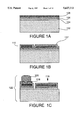
- FIGS. 1A-1E are cross sectional schematic diagrams depicting the steps in fabricating a suspended microstructure according to the invention.
- FIG. 2 is a plan view which illustrates the suspended detectors achieved by the fabrication process of FIGS. 1A-E.
- FIG. 3 is a plan view illustrating how the individual detectors of FIG. 2 can be combined to form a two dimensional detector array.
- FIGS. 4A-4E are similar to FIGS. 1A-E, but depict an embodiment of the invention suitable for fabricating pyroelectric detectors.
- FIGS. 5A-5E also are cross sectional schematic diagrams depicting the steps in fabricating a suspended microstructure, but directed toward an embodiment in which a bolometer array is constructed.
- FIGS. 6A-6E are cross sectional schematic diagrams depicting suspended microstructure fabrication, illustrating an embodiment in which the suspend microstructures are made nonplanar by sculpturing the surface of the wafer on which the structures are deposited.
- FIGS. 7A-7E depict a variation of the suspended microstructure fabrication process in which a removable layer is deposited to allow stacked levels of suspended structures.
- This invention is concerned with the fabrication of suspended thin film microstructure elements, or arrays of elements, on semiconductor integrated circuits.
- the fabrication is accomplished by forming the microstructures on a temporary substrate, then transferring this intermediate assemblage onto a silicon wafer and removing the temporary substrate.
- the invention may be illustrated by describing several examples of one preferred implementation, which involves thermal infrared focal plane arrays (IR FPAs) with microstructures made from temperature sensitive devices, such as resistors, semiconductor diodes, pyroelectric capacitors, or thermoelectric junctions.
- IR FPAs thermal infrared focal plane arrays
- the suspended microstructures because they are made with thin films, have very low thermal capacity and are designed to have high thermal isolation from the substrate, both important attributes for thermal detectors. Two approaches are contemplated for fabricating the thermal array microstructures.
- the electrical interconnections between the structures and the silicon integrated circuits also provide mechanical support for the suspended thin film structures.
- the interconnections are accomplished with pairs of indium or solder bumps formed separately on the detector array wafers and on the multiplexer wafers, then joined on a one-to-one basis.
- the interconnections are made with metal thin films which are deposited after the removal of the temporary substrate to join the microstructures to the silicon integrated circuits.
- the process begins, as depicted in the cross-sectional drawing of FIG. 1A, with obtaining a temporary silicon wafer substrate 102 of good crystalline quality (suitable for semiconductor circuit processing) such as is readily obtainable from numerous vendors.
- a layer 104 of SiO 2 100-200 nanometers thick is deposited on the working surface by any of several techniques-typically a thermal process is used to produce the oxide. This oxide layer provides an adhering surface for subsequent depositions, but is thin enough to avoid causing undue stress in the subsequent structures which are formed over it.
- a first Si 3 N 4 layer 106 is deposited over the SiO 2 layer, again by any of several techniques which will be readily apparent to a person of ordinary skill in the art. Although a stress free film is not essential for this embodiment, low stress in this layer is highly desirable, since it will allow a minimal amount of curvature in the final free-standing structure and will thereby afford the greatest freedom in the choice of device architecture.
- a layer 108 of VO 2 is then deposited on the Si 3 N 4 layer at a temperature selected to yield the best thermal and electrical properties (typically about 550° C.). Note that this step illustrates one of the most valuable aspects of this invention-namely the ability to select an optimal process (in this case high deposition temperature) for the fabrication of a first microstructure (in this case thermal detector arrays) even though that process is incompatible with a second microstructure (in this case a silicon-based multiplexer integrated circuit readout) on which the suspended microstructures are eventually attached.
- a temperature selected to yield the best thermal and electrical properties typically about 550° C.
- the VO 2 layer 108 is patterned into detectors (several formats are known to those skilled in the art) by standard photolithographic techniques--typically using a dry etch procedure.
- contact metal layers typically Ti and Ni
- contact metal layers are deposited and patterned photolithographically, leaving contact layers such as the contact layer 110.
- the patterned detectors and contact metals are overcoated with a second layer 112 of Si 3 N 4 .
- the overcoated wafer is then photolithographically patterned with a mask containing contact hole patterns and via holes are etched in the overcoat nitride by reactive ion etching (RIE), stopping at the contact metal surface.
- RIE reactive ion etching
- the free standing structures can now be delineated before attaching them to the Si-based multiplexer as detailed here, or they can be delineated at a later stage of device fabrication as described in Embodiment 2. Either procedure is applicable to all embodiments described in this application.
- Another photolithographic mask, containing patterns for the free standing detector structures, such as shown generally at the location 116, is applied and the patterns are delineated, also using reactive ion etching through the nitride and SiO 2 films.
- the bump is selected from the group consisting of alloys of indium, tin, lead, bismuth, and gallium.
- the processed silicon substrate 1522 contains microstructures ready for attaching to a second silicon wafer containing a second set of microstructures through a "hybridization" process, which is well known to those versed in the art.
- a multiplexer wafer 124 containing corresponding microstructure arrays of circuits (typically designed to suit the particular thermal detector application intended) and similarly prepared for hybridization is obtained.
- the wafer 122 with the microcircuit arrays of thermal detectors is hybridized to the water 124 with the microcircuit multiplexer arrays--typically by use of a micropositioning aligner which applies force and heat to form compression welds between corresponding In columns, such as the column 120 and an indium column 126 on the multiplexer wafer, which function as connecting elements between the wafers.
- the final height of the welded In bumps essentially determines the spacing between the two wafers, which ultimately establishes the separation of the suspended microstructures from the multiplexer.
- the hybrid structure is filled with epoxy 128, typically by vacuum injection into the spaces between the wafers and around the indium bumps. The epoxy is cured, typically with some heating, depending on the requirements of the specific epoxy.
- FIG. 2 is a plan view toward the detector side of FIG. 1E.
- FIG. 3 illustrates how the individual detectors can be combined to form a two dimensional detector array 130.
- a first variant of the above embodiment may be used where the fabrication is designed for a thermal detector device based on the variation in electrical properties with temperature of a thermally isolated piece of silicon, silicon diode, silicon transistor or other junction device readily obtained in wafer form from a commercial foundry.
- the devices are fabricated on a SOI (silicon on insulator) wafer which consists of a single crystal Si film on a thin SiO 2 film deposited on a bulk Si wafer.
- the temperature sensitive devices (diode, transistor, etc.) are made from the top Si thin film using standard Si microelectronic fabrication processes adapted to SOI devices.
- the buried oxide layer provides an etch stop during the removal of the Si substrate..
- SOI wafers are now commercially available from several sources. The simplest array (and, for some applications, one of the best) consists of silicon diodes.
- thermal detectors based on the pyroelectric effect in ferroelectric materials are also feasible, with the device taking the form of a capacitor prepared with a thin film ferroelectric material as the dielectric.
- pyroelectric refers to either a pyroelectric of a ferroelectric film.
- the example described here utilizes a transverse capacitor in which the polar axis of the material is in the plane of the film and the electrodes are placed on the: same side of the dielectric.
- Certain polycrystalline ferroelectric materials, whose crystalline structure in the paraelectric phase is cubic can be poled in any particular direction with application of an appropriate electric field at temperatures close to their ferroelectric/paraelectric phase transition.
- the transverse configuration is most suitable with ferroelectric materials exhibiting high dielectric constants and offers several advantages over conventional capacitor detectors, including: higher voltage output, simpler fabrication processing, and lower sensitivity to pin holes in the ferroelectric thin film.
- SiO 2 and nitride layers 404 and 406 are first deposited on a Si substrate 402.
- a pyroelectric film 408 is deposited using one of the methods known in the art, such as sputter deposition or sol-gel. Proceeding to FIG. 4B, the pyroelectric film is first delineated into individual detectors using, for example, ion beam milling to remove the material outside the detector pattern and stopping on the underlying nitride layer. Electrodes made with a thin metal film of high thermal resistance and compatible with the pyroelectric material, such as Pt, are deposited and lithographically delineated, as shown at 410.
- the electrodes extend beyond the edges of the capacitor along the suspended structure to where the indium bumps will be deposited.
- a thicker metal film 413 such as Al, is sputter deposited to ensure adequate electrical continuity across the edges of the pyroelectric film.
- the Pt film may not be continuous in these areas since it is typically much thinner than the pyroelectric film.
- the Al film is delineated lithographically and reactive ion etched to form narrow strips which span the edge regions but will not add significantly to the thermal mass or thermal conductance of the detector.
- a second nitride film 412 may be deposited to balance stresses in the suspended structure. Via holes and indium bumps are then prepared as detailed above and the process proceeds as described in the first example of Embodiment 1.
- the overcoated wafer is then photolithographically processed, followed by the deposition of metal contact pads, such as the pad 418, and indium bumps, such as the bump 420.
- FIG. 4D a multiplexer wafer 424 is hybridized to the wafer 422 and the hybrid structure is filled with epoxy 428.
- FIG. 4E depicts the final assembly after the substrate and the epoxy have been removed.
- FIGS. 5A through 5E The fabrication of bolometer arrays, depicted in FIGS. 5A through 5E, proceeds similar to the process for Embodiment 1, including, as in FIG. 5A, depositions on a silicon wafer substrate 502 of an SiO 2 layer 504, an Si 3 N 4 layer 506, and a VO 2 layer 508, followed by contact metal pads, such as the contact pad 510.
- the pads are made annular in shape, for reasons explained below, rather than as solid rectangles. This is followed by the deposition of a nitride overcoat 512 as in Embodiment 1.
- spacer posts such as the post 532, are deposited on the multiplexer wafer 524.
- the posts can be made of SiO 2 , glass or a metal such as aluminum.
- a suitable metal film 533 such as Al is deposited and delineated to form caps on the top surfaces of the posts and also to connect electrically to the input leads of the Si integrated circuit.
- the detector wafer 522 with the suspended microstructures is bonded to the multiplexer wafer 524 using an epoxy adhesive 528.
- the bonding is accomplished in a fixture similar to the hybridization fixture used in Embodiment 1.
- the two wafers are positioned so that the contact metal pads of the detectors and multiplexer cells are aligned.
- the bonding apparatus applies a uniform pressure normal to the wafers so that the tops of the posts, on either the detector or multiplexer wafer, come into intimate contact with the other wafer. While the apparatus holds the two wafers together in a registered manner, epoxy is injected between the layers and cured to solidify the attachment.
- the silicon substrate is then removed from the detectors, as in Embodiment 1, with a combination of mechanical thinning and reactive ion etching.
- the microstructure pattern is lithographically defined and delineated using dry etching methods.
- Vias, such as the contact hole 534, are then opened in the transferred thin film structures through the oxide and first nitride layers, going through the second nitride film 512 in the holes within the annular contact pads and stopping on the detector contact metal 518. This is followed by dry etching in an oxygen plasma to remove any thin epoxy layer that may exist in the vias between the bolometer and the multiplexer contact pads.
- the interconnections are made by depositing a relatively thick (1-1.5 microns) film 536, using a malleable metal such as Al or In, applying a lithographic mask defining the interconnect areas, and etching the metal outside the interconnect area with a suitable etchant.
- the metal thus deposited joins both the detector and the multiplexer metal pads.
- These interconnections serve the same purpose as the indium bump welds in Embodiment 1; namely, to make electrical contacts between the multiplexer cells and the detectors, as well as providing mechanical connections to the suspended detector structures once the epoxy is removed.
- the wafers are then diced into individual devices and the epoxy is removed using oxygen plasma as in Embodiment 1, leaving the completed detector as shown in FIG. 5E.
- An advantage of this process is that it avoids the use of the large force needed for compression welding of indium bumps.
- the suspended microstructures are made nonplanar by sculpturing the surface of the Si wafer on which the thin film microstructures are deposited.
- the starting Si wafer 602 is first etched, after applying the appropriate lithographic mask, so that the suspended parts of the microstructures will be located on a lower level than the parts of the structures that are to be attached to the multiplexer chip.
- An anisotropic etch,. or an orientation-dependent etching is used to produce a sloped etch profile so that the Si surface topography does not change abruptly.
- the Si topography consists of posts, such as the post 638, whose top surfaces are the original surface of the Si wafer and whose height is the amount of Si etched, which is typically 2-5 microns.
- depositions are made on a silicon wafer substrate 602 of an SiO 2 layer 604, an Si 3 N 4 layer 606, and a VO 2 layer 608, followed by contact metal pads, such as the contact pad 610.
- This is followed by the deposition of a nitride overcoat 612.
- a suitable metal film 633 such as Al is deposited and delineated to form caps on the top surfaces of the posts and also to connect electrically to the input leads of the Si integrated circuit.
- the detector wafer 622 with the suspended microstructures is bonded to the multiplexer wafer 624 using an epoxy adhesive 628.
- the silicon substrate is then removed from the detectors, as shown in FIG. 6C, and vias, such as the contact hole 634, are opened in the transferred thin film structures through the oxide and first nitride layers, going through the second nitride film 612 in the holes within the annular contact pads and stopping on the detector contact 633. This is followed by dry etching in an oxygen plasma to remove any thin epoxy layer that may exist in the vias between the bolometer and the multiplexer contact pads.
- the interconnections are made by depositing a relatively thick film 636 to join both the detector and the multiplexer metal pads.
- the wafers are then diced into individual devices and the epoxy is removed using oxygen plasma, leaving the completed detector shown in FIG. 6E.
- the basic scheme of embodiment 1 or 2 is enhanced by the additional deposition of a removable layer to allow stacked levels of suspended structures.
- This enhanced structure provides a number of advantages for some applications. When used with thermal detectors, for example, it allows nearly all of the pixel area to be filled with detector material and at the same time permits extended lead length for better thermal isolation.
- This embodiment is illustrated as a derivative of Embodiment 1, but note that those versed in the art will be readily able to derive a similar structure from variants of Embodiment 1 or from Embodiment 2 or its variants.
- Embodiment 3 begins similar to Embodiment 1, as shown in FIG. 7A, with a temporary substrate 702 on which are deposited a layer 704 of SiO 2 , a layer 706 of Si 3 N 4 , and a layer 708 of VO 2 .
- the VO 2 or other material is patterned into detectors, receives contact metalization 710, and is overcoated with another layer 712 of Si 3 N 4 (in the case of VO 2 ).
- the shape of the detector patterns is different, however, due to the absence of the need for narrow thermal isolation leads at the detector level of the structure.
- the detectors are isolated from each other by reactive ion etching or ion milling through both Si 3 N 4 and SiO 2 down to the silicon substrate, as shown at the location 740.
- the patterned detectors are overcoated with a few microns of a polymer film 742, such as photosensitive polyimide or another organic material which can be photolithographically patterned and which is resilient to subsequent processing, including moderate deposition temperatures and deposition and removal of conventional photoresist.
- a polymer film 742 such as photosensitive polyimide or another organic material which can be photolithographically patterned and which is resilient to subsequent processing, including moderate deposition temperatures and deposition and removal of conventional photoresist.
- the polyimide is photolithographically patterned to open contact holes, such as the hole 744, to the contact pads on the detectors (two per detector). If necessary, the protective Si 3 N 4 layer is removed in the contact area by reactive ion etching or another chemical or mechanical process.
- Two thin, meandering contact metal lines (typically of nichrome) for each detector, such as the line 718, are deposited and delineated on the polyimide so that one end of each line contacts a detector pad and the other end of the line terminates in a metal pad suitable for an indium column. If necessary for structural strength, this meandering contact is overcoated with Si 3 N 4 deposited at a temperature compatible with polyimide (typically ⁇ 300 C).
- the nitride is subsequently patterned photolithographically and reactive ion etched into a similar meandering pattern to open contact holes to the metal pads for indium columns.
- indium bumps such as the bump 720, are deposited on the nichrome film through the contact holes in the nitride layer.
- a multiplexer wafer 724 containing corresponding microstructure arrays of circuits is hybridized to the wafer 722 by joining corresponding In columns, such as the columns 720 and 726, then filling with epoxy 728.
- the substrate 702 is then removed and the epoxy is removed, leaving suspended structures.
Abstract
Description
Claims (10)
Priority Applications (5)
| Application Number | Priority Date | Filing Date | Title |
|---|---|---|---|
| US08/555,668 US5627112A (en) | 1995-11-13 | 1995-11-13 | Method of making suspended microstructures |
| EP96116591A EP0773436A3 (en) | 1995-11-13 | 1996-10-16 | Suspended microstructures |
| AU70565/96A AU715673B2 (en) | 1995-11-13 | 1996-11-01 | Suspended microstructures |
| JP30034496A JP3605487B2 (en) | 1995-11-13 | 1996-11-12 | Method for manufacturing a floating microstructure and a floating microstructure processing assembly |
| CA002190077A CA2190077C (en) | 1995-11-13 | 1996-11-12 | Suspended microstructures |
Applications Claiming Priority (1)
| Application Number | Priority Date | Filing Date | Title |
|---|---|---|---|
| US08/555,668 US5627112A (en) | 1995-11-13 | 1995-11-13 | Method of making suspended microstructures |
Publications (1)
| Publication Number | Publication Date |
|---|---|
| US5627112A true US5627112A (en) | 1997-05-06 |
Family
ID=24218165
Family Applications (1)
| Application Number | Title | Priority Date | Filing Date |
|---|---|---|---|
| US08/555,668 Expired - Lifetime US5627112A (en) | 1995-11-13 | 1995-11-13 | Method of making suspended microstructures |
Country Status (5)
| Country | Link |
|---|---|
| US (1) | US5627112A (en) |
| EP (1) | EP0773436A3 (en) |
| JP (1) | JP3605487B2 (en) |
| AU (1) | AU715673B2 (en) |
| CA (1) | CA2190077C (en) |
Cited By (31)
| Publication number | Priority date | Publication date | Assignee | Title |
|---|---|---|---|---|
| US5688699A (en) * | 1996-01-16 | 1997-11-18 | Raytheon Company | Microbolometer |
| US6144030A (en) * | 1997-10-28 | 2000-11-07 | Raytheon Company | Advanced small pixel high fill factor uncooled focal plane array |
| US6214733B1 (en) * | 1999-11-17 | 2001-04-10 | Elo Technologies, Inc. | Process for lift off and handling of thin film materials |
| US6252229B1 (en) | 1998-07-10 | 2001-06-26 | Boeing North American, Inc. | Sealed-cavity microstructure and microbolometer and associated fabrication methods |
| WO2001063232A1 (en) * | 2000-02-24 | 2001-08-30 | University Of Virginia Patent Foundation | High sensitivity infrared sensing apparatus and related method thereof |
| US6287940B1 (en) | 1999-08-02 | 2001-09-11 | Honeywell International Inc. | Dual wafer attachment process |
| US6313463B1 (en) | 1996-12-31 | 2001-11-06 | Honeywell International Inc. | Flexible high performance microbolometer detector material fabricated via controlled ion beam sputter deposition process |
| US6476374B1 (en) | 2000-04-25 | 2002-11-05 | Innovative Technology Licensing, Llc | Room temperature, low-light-level visible imager |
| US6483116B1 (en) | 2000-04-25 | 2002-11-19 | Innovative Technology Licensing, Llc | High performance ultraviolet imager for operation at room temperature |
| US20020175284A1 (en) * | 2001-03-21 | 2002-11-28 | Michel Vilain | Radition detectors and methods for manufacturing them |
| US6504141B1 (en) | 2000-09-29 | 2003-01-07 | Rockwell Science Center, Llc | Adaptive amplifier circuit with enhanced dynamic range |
| US6538245B1 (en) | 2000-10-26 | 2003-03-25 | Rockwell Science Center, Llc. | Amplified CMOS transducer for single photon read-out of photodetectors |
| US20030057564A1 (en) * | 1997-04-04 | 2003-03-27 | Elm Technology Corporation | Three dimensional structure memory |
| US20030183945A1 (en) * | 1999-06-28 | 2003-10-02 | Park Sang Wook | Chip size stack package and method of fabricating the same |
| US20030218182A1 (en) * | 1992-04-08 | 2003-11-27 | Leedy Glenn J. | Strees-controlled dielectric integrated circuit |
| US20030223535A1 (en) * | 1992-04-08 | 2003-12-04 | Leedy Glenn Joseph | Lithography device for semiconductor circuit pattern generator |
| US20040097008A1 (en) * | 1997-04-04 | 2004-05-20 | Elm Technology Corporation | Three dimensional structure integrated circuit |
| US20040108071A1 (en) * | 2001-04-11 | 2004-06-10 | Thomas Wien | Label applicator and system |
| US20040118129A1 (en) * | 2002-12-20 | 2004-06-24 | Chrysler Gregory M. | Thermoelectric cooling for microelectronic packages and dice |
| US20040261830A1 (en) * | 2001-06-01 | 2004-12-30 | Marlow Industries, Inc. | Thermoelectric device having P-type and N-type materials |
| US20050023656A1 (en) * | 2002-08-08 | 2005-02-03 | Leedy Glenn J. | Vertical system integration |
| US6873359B1 (en) | 2000-09-29 | 2005-03-29 | Rockwell Science Center, Llc. | Self-adjusting, adaptive, minimal noise input amplifier circuit |
| US6888572B1 (en) | 2000-10-26 | 2005-05-03 | Rockwell Science Center, Llc | Compact active pixel with low-noise image formation |
| US6900839B1 (en) | 2000-09-29 | 2005-05-31 | Rockwell Science Center, Llc | High gain detector amplifier with enhanced dynamic range for single photon read-out of photodetectors |
| US20050133479A1 (en) * | 2003-12-19 | 2005-06-23 | Youngner Dan W. | Equipment and process for creating a custom sloped etch in a substrate |
| US6965707B1 (en) | 2000-09-29 | 2005-11-15 | Rockwell Science Center, Llc | Compact active pixel with low-noise snapshot image formation |
| US20060131579A1 (en) * | 2004-12-17 | 2006-06-22 | Commissariat A L'energie Atomique | Semiconductor photodetector, device for multispectrum detection of electromagnetic radiation using such a photodetector and method for using such a device |
| US20070164417A1 (en) * | 2004-02-27 | 2007-07-19 | Todd Michael A | Design and fabrication method for microsensor |
| US20080117322A1 (en) * | 2006-11-17 | 2008-05-22 | Shimadzu Corporation | Image pickup device and imaging apparatus using the same |
| US20090302468A1 (en) * | 2008-06-05 | 2009-12-10 | Samsung Electro-Mechanics Co., Ltd. | Printed circuit board comprising semiconductor chip and method of manufacturing the same |
| US11231326B2 (en) | 2017-05-22 | 2022-01-25 | Mitsubishi Electric Corporation | Infrared imaging element, infrared imaging array, and method for manufacturing infrared imaging element |
Families Citing this family (9)
| Publication number | Priority date | Publication date | Assignee | Title |
|---|---|---|---|---|
| US5904495A (en) * | 1997-06-11 | 1999-05-18 | Massachusetts Institute Of Technology | Interconnection technique for hybrid integrated devices |
| SE0000148D0 (en) * | 2000-01-17 | 2000-01-17 | Forskarpatent I Syd Ab | Manufacturing method for IR detector matrices |
| US6569754B2 (en) * | 2000-08-24 | 2003-05-27 | The Regents Of The University Of Michigan | Method for making a module including a microplatform |
| EP1296374B1 (en) | 2001-09-14 | 2012-09-05 | STMicroelectronics Srl | Process for bonding and electrically connecting microsystems integrated in several distinct substrates |
| AU2003206552A1 (en) | 2002-02-14 | 2003-09-04 | Silex Microsystems Ab | Deflectable microstructure and method of manufacturing the same through bonding of wafers |
| US20070065968A1 (en) * | 2003-05-26 | 2007-03-22 | Kit-Wai Kok | Fabrication of silicon microphone |
| EP2363888A1 (en) * | 2010-03-02 | 2011-09-07 | SensoNor Technologies AS | Focal plane array and method for manufacturing the same |
| EP2363887A1 (en) | 2010-03-02 | 2011-09-07 | SensoNor Technologies AS | Focal plane array and method for manufacturing the same |
| DE102012217154A1 (en) * | 2012-09-24 | 2014-03-27 | Robert Bosch Gmbh | Semiconductor device and method of manufacturing a semiconductor device |
Citations (15)
| Publication number | Priority date | Publication date | Assignee | Title |
|---|---|---|---|---|
| US4426758A (en) * | 1982-08-23 | 1984-01-24 | Castoe John H | Seal puller |
| US4847500A (en) * | 1985-09-12 | 1989-07-11 | Plessey Overseas Limited | Thermal detector |
| US4859629A (en) * | 1986-04-18 | 1989-08-22 | M/A-Com, Inc. | Method of fabricating a semiconductor beam lead device |
| US5018256A (en) * | 1990-06-29 | 1991-05-28 | Texas Instruments Incorporated | Architecture and process for integrating DMD with control circuit substrates |
| US5037779A (en) * | 1989-05-19 | 1991-08-06 | Whalley Peter D | Method of encapsulating a sensor device using capillary action and the device so encapsulated |
| US5045503A (en) * | 1987-12-14 | 1991-09-03 | Mitsubishi Denki Kabushiki Kaisha | Microwave monolithic integrated circuit with heat radiating electrode |
| US5059556A (en) * | 1988-09-28 | 1991-10-22 | Siemens-Bendix Automotive Electronics, L.P. | Low stress polysilicon microstructures |
| US5090819A (en) * | 1990-08-20 | 1992-02-25 | Conductus, Inc. | Superconducting bolometer |
| US5099120A (en) * | 1989-06-20 | 1992-03-24 | U.S. Philips Corporation | Thermal-radiation detectors, detection systems and their manufacture |
| GB2265754A (en) * | 1992-03-30 | 1993-10-06 | Awa Microelectronics | Beam structure in silicon devices |
| US5258325A (en) * | 1990-12-31 | 1993-11-02 | Kopin Corporation | Method for manufacturing a semiconductor device using a circuit transfer film |
| WO1993025878A1 (en) * | 1992-06-11 | 1993-12-23 | Honeywell, Inc. | Thermal isolation microstructure |
| WO1993025877A1 (en) * | 1992-06-11 | 1993-12-23 | Honeywell, Inc. | Use of vanadium oxide in microbolometer sensors |
| US5438875A (en) * | 1991-03-28 | 1995-08-08 | The Foxboro Company | Removing sacrificial material through temporary channels as a method of making an overpressure-protected differential pressure sensor |
| US5508231A (en) * | 1994-03-07 | 1996-04-16 | National Semiconductor Corporation | Apparatus and method for achieving mechanical and thermal isolation of portions of integrated monolithic circuits |
Family Cites Families (3)
| Publication number | Priority date | Publication date | Assignee | Title |
|---|---|---|---|---|
| DE3067381D1 (en) * | 1979-11-15 | 1984-05-10 | Secr Defence Brit | Series-connected combination of two-terminal semiconductor devices and their fabrication |
| JPS5843554A (en) * | 1981-09-08 | 1983-03-14 | Mitsubishi Electric Corp | Semiconductor device |
| JPS5948950A (en) * | 1982-09-13 | 1984-03-21 | Agency Of Ind Science & Technol | Manufacture of three-dimensional integrated circuit structure |
-
1995
- 1995-11-13 US US08/555,668 patent/US5627112A/en not_active Expired - Lifetime
-
1996
- 1996-10-16 EP EP96116591A patent/EP0773436A3/en not_active Withdrawn
- 1996-11-01 AU AU70565/96A patent/AU715673B2/en not_active Expired
- 1996-11-12 CA CA002190077A patent/CA2190077C/en not_active Expired - Lifetime
- 1996-11-12 JP JP30034496A patent/JP3605487B2/en not_active Expired - Lifetime
Patent Citations (15)
| Publication number | Priority date | Publication date | Assignee | Title |
|---|---|---|---|---|
| US4426758A (en) * | 1982-08-23 | 1984-01-24 | Castoe John H | Seal puller |
| US4847500A (en) * | 1985-09-12 | 1989-07-11 | Plessey Overseas Limited | Thermal detector |
| US4859629A (en) * | 1986-04-18 | 1989-08-22 | M/A-Com, Inc. | Method of fabricating a semiconductor beam lead device |
| US5045503A (en) * | 1987-12-14 | 1991-09-03 | Mitsubishi Denki Kabushiki Kaisha | Microwave monolithic integrated circuit with heat radiating electrode |
| US5059556A (en) * | 1988-09-28 | 1991-10-22 | Siemens-Bendix Automotive Electronics, L.P. | Low stress polysilicon microstructures |
| US5037779A (en) * | 1989-05-19 | 1991-08-06 | Whalley Peter D | Method of encapsulating a sensor device using capillary action and the device so encapsulated |
| US5099120A (en) * | 1989-06-20 | 1992-03-24 | U.S. Philips Corporation | Thermal-radiation detectors, detection systems and their manufacture |
| US5018256A (en) * | 1990-06-29 | 1991-05-28 | Texas Instruments Incorporated | Architecture and process for integrating DMD with control circuit substrates |
| US5090819A (en) * | 1990-08-20 | 1992-02-25 | Conductus, Inc. | Superconducting bolometer |
| US5258325A (en) * | 1990-12-31 | 1993-11-02 | Kopin Corporation | Method for manufacturing a semiconductor device using a circuit transfer film |
| US5438875A (en) * | 1991-03-28 | 1995-08-08 | The Foxboro Company | Removing sacrificial material through temporary channels as a method of making an overpressure-protected differential pressure sensor |
| GB2265754A (en) * | 1992-03-30 | 1993-10-06 | Awa Microelectronics | Beam structure in silicon devices |
| WO1993025878A1 (en) * | 1992-06-11 | 1993-12-23 | Honeywell, Inc. | Thermal isolation microstructure |
| WO1993025877A1 (en) * | 1992-06-11 | 1993-12-23 | Honeywell, Inc. | Use of vanadium oxide in microbolometer sensors |
| US5508231A (en) * | 1994-03-07 | 1996-04-16 | National Semiconductor Corporation | Apparatus and method for achieving mechanical and thermal isolation of portions of integrated monolithic circuits |
Cited By (77)
| Publication number | Priority date | Publication date | Assignee | Title |
|---|---|---|---|---|
| US20050176174A1 (en) * | 1992-04-08 | 2005-08-11 | Elm Technology Corporation | Methodof making an integrated circuit |
| US20040197951A1 (en) * | 1992-04-08 | 2004-10-07 | Leedy Glenn Joseph | Membrane IC fabrication |
| US20030218182A1 (en) * | 1992-04-08 | 2003-11-27 | Leedy Glenn J. | Strees-controlled dielectric integrated circuit |
| US7763948B2 (en) | 1992-04-08 | 2010-07-27 | Taiwan Semiconductor Manufacturing Co., Ltd. | Flexible and elastic dielectric integrated circuit |
| US7670893B2 (en) | 1992-04-08 | 2010-03-02 | Taiwan Semiconductor Manufacturing Co., Ltd. | Membrane IC fabrication |
| US20080302559A1 (en) * | 1992-04-08 | 2008-12-11 | Elm Technology Corporation | Flexible and elastic dielectric integrated circuit |
| US20050130351A1 (en) * | 1992-04-08 | 2005-06-16 | Elm Technology Corporation | Methods for maskless lithography |
| US20030223535A1 (en) * | 1992-04-08 | 2003-12-04 | Leedy Glenn Joseph | Lithography device for semiconductor circuit pattern generator |
| US7820469B2 (en) | 1992-04-08 | 2010-10-26 | Taiwan Semiconductor Manufacturing Co., Ltd. | Stress-controlled dielectric integrated circuit |
| US20040132303A1 (en) * | 1992-04-08 | 2004-07-08 | Elm Technology Corporation | Membrane 3D IC fabrication |
| US20040150068A1 (en) * | 1992-04-08 | 2004-08-05 | Elm Technology Corporation | Membrane 3D IC fabrication |
| US20050082626A1 (en) * | 1992-04-08 | 2005-04-21 | Elm Technology Corporation | Membrane 3D IC fabrication |
| US20050082641A1 (en) * | 1992-04-08 | 2005-04-21 | Elm Technology Corporation | Flexible and elastic dielectric integrated circuit |
| US7911012B2 (en) | 1992-04-08 | 2011-03-22 | Taiwan Semiconductor Manufacturing Co., Ltd. | Flexible and elastic dielectric integrated circuit |
| US20040192045A1 (en) * | 1992-04-08 | 2004-09-30 | Elm Technology Corporation. | Apparatus and methods for maskless pattern generation |
| US5688699A (en) * | 1996-01-16 | 1997-11-18 | Raytheon Company | Microbolometer |
| US6495070B1 (en) | 1996-12-31 | 2002-12-17 | Honeywell International Inc. | Flexible high performance microbolometer detector material fabricated via controlled ion beam sputter deposition process |
| US6322670B2 (en) * | 1996-12-31 | 2001-11-27 | Honeywell International Inc. | Flexible high performance microbolometer detector material fabricated via controlled ion beam sputter deposition process |
| US6313463B1 (en) | 1996-12-31 | 2001-11-06 | Honeywell International Inc. | Flexible high performance microbolometer detector material fabricated via controlled ion beam sputter deposition process |
| US20030173608A1 (en) * | 1997-04-04 | 2003-09-18 | Elm Technology Corporation | Three dimensional structure integrated circuit |
| US8796862B2 (en) | 1997-04-04 | 2014-08-05 | Glenn J Leedy | Three dimensional memory structure |
| US8318538B2 (en) | 1997-04-04 | 2012-11-27 | Elm Technology Corp. | Three dimensional structure memory |
| US20040070063A1 (en) * | 1997-04-04 | 2004-04-15 | Elm Technology Corporation | Three dimensional structure integrated circuit |
| US20040097008A1 (en) * | 1997-04-04 | 2004-05-20 | Elm Technology Corporation | Three dimensional structure integrated circuit |
| US8410617B2 (en) | 1997-04-04 | 2013-04-02 | Elm Technology | Three dimensional structure memory |
| US8035233B2 (en) * | 1997-04-04 | 2011-10-11 | Elm Technology Corporation | Adjacent substantially flexible substrates having integrated circuits that are bonded together by non-polymeric layer |
| US9401183B2 (en) | 1997-04-04 | 2016-07-26 | Glenn J. Leedy | Stacked integrated memory device |
| US7705466B2 (en) | 1997-04-04 | 2010-04-27 | Elm Technology Corporation | Three dimensional multi layer memory and control logic integrated circuit structure |
| US8629542B2 (en) | 1997-04-04 | 2014-01-14 | Glenn J. Leedy | Three dimensional structure memory |
| US20040151043A1 (en) * | 1997-04-04 | 2004-08-05 | Elm Technology Corporation | Three dimensional structure memory |
| US20030057564A1 (en) * | 1997-04-04 | 2003-03-27 | Elm Technology Corporation | Three dimensional structure memory |
| US8791581B2 (en) | 1997-04-04 | 2014-07-29 | Glenn J Leedy | Three dimensional structure memory |
| US8288206B2 (en) | 1997-04-04 | 2012-10-16 | Elm Technology Corp | Three dimensional structure memory |
| US8824159B2 (en) | 1997-04-04 | 2014-09-02 | Glenn J. Leedy | Three dimensional structure memory |
| US9087556B2 (en) | 1997-04-04 | 2015-07-21 | Glenn J Leedy | Three dimension structure memory |
| US8841778B2 (en) | 1997-04-04 | 2014-09-23 | Glenn J Leedy | Three dimensional memory structure |
| US8907499B2 (en) | 1997-04-04 | 2014-12-09 | Glenn J Leedy | Three dimensional structure memory |
| US8928119B2 (en) | 1997-04-04 | 2015-01-06 | Glenn J. Leedy | Three dimensional structure memory |
| US8933570B2 (en) | 1997-04-04 | 2015-01-13 | Elm Technology Corp. | Three dimensional structure memory |
| US6144030A (en) * | 1997-10-28 | 2000-11-07 | Raytheon Company | Advanced small pixel high fill factor uncooled focal plane array |
| US6252229B1 (en) | 1998-07-10 | 2001-06-26 | Boeing North American, Inc. | Sealed-cavity microstructure and microbolometer and associated fabrication methods |
| US6596117B2 (en) | 1998-07-10 | 2003-07-22 | Drs Sensors & Targeting Systems, Inc. | Method for fabricating a sealed-cavity microstructure |
| US20030183945A1 (en) * | 1999-06-28 | 2003-10-02 | Park Sang Wook | Chip size stack package and method of fabricating the same |
| US6828686B2 (en) * | 1999-06-28 | 2004-12-07 | Hyundai Electronics Industries Co., Ltd. | Chip size stack package and method of fabricating the same |
| US6287940B1 (en) | 1999-08-02 | 2001-09-11 | Honeywell International Inc. | Dual wafer attachment process |
| US6214733B1 (en) * | 1999-11-17 | 2001-04-10 | Elo Technologies, Inc. | Process for lift off and handling of thin film materials |
| WO2001063232A1 (en) * | 2000-02-24 | 2001-08-30 | University Of Virginia Patent Foundation | High sensitivity infrared sensing apparatus and related method thereof |
| US20030141453A1 (en) * | 2000-02-24 | 2003-07-31 | Reed Michael L. | High sensitivity infrared sensing apparatus and related method thereof |
| US6900440B2 (en) * | 2000-02-24 | 2005-05-31 | University Of Virginia Patent Foundation | High sensitivity infrared sensing apparatus and related method thereof |
| US6483116B1 (en) | 2000-04-25 | 2002-11-19 | Innovative Technology Licensing, Llc | High performance ultraviolet imager for operation at room temperature |
| US6476374B1 (en) | 2000-04-25 | 2002-11-05 | Innovative Technology Licensing, Llc | Room temperature, low-light-level visible imager |
| EP1323193A2 (en) * | 2000-09-25 | 2003-07-02 | Innovative Technology Licensing, LLC | High performance ultraviolet imager for operation at room temperature |
| US6504141B1 (en) | 2000-09-29 | 2003-01-07 | Rockwell Science Center, Llc | Adaptive amplifier circuit with enhanced dynamic range |
| US6873359B1 (en) | 2000-09-29 | 2005-03-29 | Rockwell Science Center, Llc. | Self-adjusting, adaptive, minimal noise input amplifier circuit |
| US6900839B1 (en) | 2000-09-29 | 2005-05-31 | Rockwell Science Center, Llc | High gain detector amplifier with enhanced dynamic range for single photon read-out of photodetectors |
| US6965707B1 (en) | 2000-09-29 | 2005-11-15 | Rockwell Science Center, Llc | Compact active pixel with low-noise snapshot image formation |
| US6538245B1 (en) | 2000-10-26 | 2003-03-25 | Rockwell Science Center, Llc. | Amplified CMOS transducer for single photon read-out of photodetectors |
| US6888572B1 (en) | 2000-10-26 | 2005-05-03 | Rockwell Science Center, Llc | Compact active pixel with low-noise image formation |
| USRE43314E1 (en) | 2000-10-26 | 2012-04-17 | Altasens, Inc. | Compact active pixel with low-noise image formation |
| US20020175284A1 (en) * | 2001-03-21 | 2002-11-28 | Michel Vilain | Radition detectors and methods for manufacturing them |
| US6753526B2 (en) * | 2001-03-21 | 2004-06-22 | Commissariat A L'energie Atomique | Radiation detectors and methods for manufacturing them |
| US20040108071A1 (en) * | 2001-04-11 | 2004-06-10 | Thomas Wien | Label applicator and system |
| US20040261830A1 (en) * | 2001-06-01 | 2004-12-30 | Marlow Industries, Inc. | Thermoelectric device having P-type and N-type materials |
| US7619158B2 (en) * | 2001-06-01 | 2009-11-17 | Marlow Industries, Inc. | Thermoelectric device having P-type and N-type materials |
| US20050023656A1 (en) * | 2002-08-08 | 2005-02-03 | Leedy Glenn J. | Vertical system integration |
| US8080442B2 (en) | 2002-08-08 | 2011-12-20 | Elm Technology Corporation | Vertical system integration |
| US8587102B2 (en) | 2002-08-08 | 2013-11-19 | Glenn J Leedy | Vertical system integration |
| US8269327B2 (en) | 2002-08-08 | 2012-09-18 | Glenn J Leedy | Vertical system integration |
| US20040118129A1 (en) * | 2002-12-20 | 2004-06-24 | Chrysler Gregory M. | Thermoelectric cooling for microelectronic packages and dice |
| US6981380B2 (en) * | 2002-12-20 | 2006-01-03 | Intel Corporation | Thermoelectric cooling for microelectronic packages and dice |
| US20050133479A1 (en) * | 2003-12-19 | 2005-06-23 | Youngner Dan W. | Equipment and process for creating a custom sloped etch in a substrate |
| US20070164417A1 (en) * | 2004-02-27 | 2007-07-19 | Todd Michael A | Design and fabrication method for microsensor |
| US7619240B2 (en) * | 2004-12-17 | 2009-11-17 | Commissariat A L'energie Atomique | Semiconductor photodetector, device for multispectrum detection of electromagnetic radiation using such a photodetector and method for using such a device |
| US20060131579A1 (en) * | 2004-12-17 | 2006-06-22 | Commissariat A L'energie Atomique | Semiconductor photodetector, device for multispectrum detection of electromagnetic radiation using such a photodetector and method for using such a device |
| US20080117322A1 (en) * | 2006-11-17 | 2008-05-22 | Shimadzu Corporation | Image pickup device and imaging apparatus using the same |
| US20090302468A1 (en) * | 2008-06-05 | 2009-12-10 | Samsung Electro-Mechanics Co., Ltd. | Printed circuit board comprising semiconductor chip and method of manufacturing the same |
| US11231326B2 (en) | 2017-05-22 | 2022-01-25 | Mitsubishi Electric Corporation | Infrared imaging element, infrared imaging array, and method for manufacturing infrared imaging element |
Also Published As
| Publication number | Publication date |
|---|---|
| CA2190077C (en) | 2002-11-05 |
| EP0773436A2 (en) | 1997-05-14 |
| AU7056596A (en) | 1997-05-22 |
| JP3605487B2 (en) | 2004-12-22 |
| JPH09210769A (en) | 1997-08-15 |
| AU715673B2 (en) | 2000-02-10 |
| EP0773436A3 (en) | 2000-05-31 |
| CA2190077A1 (en) | 1997-05-14 |
Similar Documents
| Publication | Publication Date | Title |
|---|---|---|
| US5627112A (en) | Method of making suspended microstructures | |
| EP1198835B1 (en) | Dual wafer attachment process | |
| US8809135B2 (en) | MEMS device and interposer and method for integrating MEMS device and interposer | |
| EP1275146B1 (en) | Method of joining components | |
| US5489554A (en) | Method of making a 3-dimensional circuit assembly having electrical contacts that extend through the IC layer | |
| EP0985137B1 (en) | A thermal detector array | |
| US5587090A (en) | Multiple level mask for patterning of ceramic materials | |
| JPH02132866A (en) | Mechanical sensor for high-temperature environment | |
| US6868733B2 (en) | Sensor having membrane and method for manufacturing the same | |
| US5679267A (en) | Dual etching of ceramic materials with an elevated thin film | |
| EP3095755B1 (en) | Monolithic fabrication of thermally isolated microelectromechanical system (mems) devices | |
| EP0635885B1 (en) | High density circuit assembly | |
| Hata et al. | Uncooled IRFPA with chip scale vacuum package | |
| US5631467A (en) | Etching of ceramic materials with an elevated thin film | |
| WO2007089204A1 (en) | Mems components and method for manufacturing same | |
| JPH10116997A (en) | Composite device | |
| JPH08116071A (en) | Manufacture of semiconductor dynamics sensor | |
| JPH0758285A (en) | Highly dense circuit device and its formation |
Legal Events
| Date | Code | Title | Description |
|---|---|---|---|
| AS | Assignment |
Owner name: ROCKWELL INTERNATIONAL CORPORATION, CALIFORNIA Free format text: ASSIGNMENT OF ASSIGNORS INTEREST;ASSIGNORS:TENNANT, WILLIAM E.;GERGIS, ISORIS S.;SEABURY, CHARLES W.;REEL/FRAME:007765/0588 Effective date: 19951113 |
|
| STCF | Information on status: patent grant |
Free format text: PATENTED CASE |
|
| AS | Assignment |
Owner name: CREDIT SUISSE FIRST BOSTON, NEW YORK Free format text: SECURITY INTEREST;ASSIGNORS:CONEXANT SYSTEMS, INC.;BROOKTREE CORPORATION;BROOKTREE WORLDWIDE SALES CORPORATION;AND OTHERS;REEL/FRAME:009719/0537 Effective date: 19981221 |
|
| AS | Assignment |
Owner name: CONEXANT SYSTEMS, INC., CALIFORNIA Free format text: ASSIGNMENT OF ASSIGNORS INTEREST;ASSIGNOR:ROCKWELL SCIENCE CENTER, LLC;REEL/FRAME:010415/0761 Effective date: 19981210 |
|
| AS | Assignment |
Owner name: BOEING COMPANY, THE, CALIFORNIA Free format text: MERGER;ASSIGNORS:ROCKWELL INTERNATIONAL CORPORATION;BOEING NORTH AMERICAN, INC.;REEL/FRAME:011164/0426;SIGNING DATES FROM 19961206 TO 19991230 |
|
| REMI | Maintenance fee reminder mailed | ||
| FEPP | Fee payment procedure |
Free format text: PAYOR NUMBER ASSIGNED (ORIGINAL EVENT CODE: ASPN); ENTITY STATUS OF PATENT OWNER: LARGE ENTITY |
|
| FPAY | Fee payment |
Year of fee payment: 4 |
|
| SULP | Surcharge for late payment | ||
| AS | Assignment |
Owner name: DRS SENSORS & TARGETING SYSTEMS, INC., CALIFORNIA Free format text: CHANGE OF NAME;ASSIGNOR:BOEING COMPANY, THE;REEL/FRAME:012333/0280 Effective date: 20010926 |
|
| AS | Assignment |
Owner name: CONEXANT SYSTEMS, INC., CALIFORNIA Free format text: RELEASE OF SECURITY INTEREST;ASSIGNOR:CREDIT SUISSE FIRST BOSTON;REEL/FRAME:012252/0413 Effective date: 20011018 Owner name: BROOKTREE CORPORATION, CALIFORNIA Free format text: RELEASE OF SECURITY INTEREST;ASSIGNOR:CREDIT SUISSE FIRST BOSTON;REEL/FRAME:012252/0413 Effective date: 20011018 Owner name: BROOKTREE WORLDWIDE SALES CORPORATION, CALIFORNIA Free format text: RELEASE OF SECURITY INTEREST;ASSIGNOR:CREDIT SUISSE FIRST BOSTON;REEL/FRAME:012252/0413 Effective date: 20011018 Owner name: CONEXANT SYSTEMS WORLDWIDE, INC., CALIFORNIA Free format text: RELEASE OF SECURITY INTEREST;ASSIGNOR:CREDIT SUISSE FIRST BOSTON;REEL/FRAME:012252/0413 Effective date: 20011018 |
|
| AS | Assignment |
Owner name: BOEING COMPANY, THE, CALIFORNIA Free format text: MERGER/CHANGE OF NAME;ASSIGNOR:BOEING NORTH AMERICAN, INC.;REEL/FRAME:012983/0674 Effective date: 19991230 Owner name: BOEING NORTH AMERICAN, INC., CALIFORNIA Free format text: MERGER AND CHANGE OF NAME;ASSIGNOR:ROCKWELL INTERNATIONAL CORPORATION;REEL/FRAME:012983/0837 Effective date: 19961206 |
|
| AS | Assignment |
Owner name: FIRST UNION NATIONAL BANK, NORTH CAROLINA Free format text: SECURITY INTEREST;ASSIGNOR:DRS SENSORS & TARGETING SYSTEMS, INC.;REEL/FRAME:013463/0211 Effective date: 20010928 |
|
| FPAY | Fee payment |
Year of fee payment: 8 |
|
| AS | Assignment |
Owner name: WACHOVIA BANK, NATIONAL ASSOCIATION, NORTH CAROLIN Free format text: PATENT SECURITY AGREEMENT;ASSIGNOR:DRS SENSORS & TARGETING SYSTEMS, INC.;REEL/FRAME:017286/0579 Effective date: 20060131 |
|
| AS | Assignment |
Owner name: WACHOVIA BANK, NATIONAL ASSOCIATION, NORTH CAROLIN Free format text: PATENT SECURITY AGREEMENT;ASSIGNOR:DRS SENSORS & TARGETING SYSTEMS, INC.;REEL/FRAME:019580/0785 Effective date: 20060615 |
|
| FPAY | Fee payment |
Year of fee payment: 12 |
|
| AS | Assignment |
Owner name: DRS RSTA, INC.,TEXAS Free format text: CHANGE OF NAME;ASSIGNOR:DRS SENSORS & TARGETING SYSTEMS, INC.;REEL/FRAME:023905/0520 Effective date: 20090512 Owner name: DRS RSTA, INC., TEXAS Free format text: CHANGE OF NAME;ASSIGNOR:DRS SENSORS & TARGETING SYSTEMS, INC.;REEL/FRAME:023905/0520 Effective date: 20090512 |
|
| AS | Assignment |
Owner name: DRS SENSORS & TARGETING SYSTEMS, INC.,TEXAS Free format text: RELEASE BY SECURED PARTY;ASSIGNOR:WELLS FARGO BANK, N.A.;REEL/FRAME:024588/0493 Effective date: 20100607 Owner name: DRS SENSORS & TARGETING SYSTEMS, INC.,TEXAS Free format text: RELEASE BY SECURED PARTY;ASSIGNOR:WELLS FARGO BANK, N.A.;REEL/FRAME:024588/0510 Effective date: 20100607 |
|
| AS | Assignment |
Owner name: DRS SENSORS & TARGETING SYSTEMS, INC.,TEXAS Free format text: RELEASE BY SECURED PARTY;ASSIGNOR:WELLS FARGO BANK, N.A.;REEL/FRAME:024611/0597 Effective date: 20100607 |
|
| AS | Assignment |
Owner name: DRS NETWORK & IMAGING SYSTEMS, LLC, FLORIDA Free format text: CHANGE OF NAME;ASSIGNOR:DRS RSTA, INC.;REEL/FRAME:035349/0060 Effective date: 20140722 |