US5650593A - Thermally enhanced chip carrier package - Google Patents
Thermally enhanced chip carrier package Download PDFInfo
- Publication number
- US5650593A US5650593A US08/383,966 US38396695A US5650593A US 5650593 A US5650593 A US 5650593A US 38396695 A US38396695 A US 38396695A US 5650593 A US5650593 A US 5650593A
- Authority
- US
- United States
- Prior art keywords
- package
- circuit substrate
- casing
- heat sink
- chip
- Prior art date
- Legal status (The legal status is an assumption and is not a legal conclusion. Google has not performed a legal analysis and makes no representation as to the accuracy of the status listed.)
- Expired - Lifetime
Links
Images


Classifications
-
- H—ELECTRICITY
- H01—ELECTRIC ELEMENTS
- H01L—SEMICONDUCTOR DEVICES NOT COVERED BY CLASS H10
- H01L23/00—Details of semiconductor or other solid state devices
- H01L23/34—Arrangements for cooling, heating, ventilating or temperature compensation ; Temperature sensing arrangements
- H01L23/36—Selection of materials, or shaping, to facilitate cooling or heating, e.g. heatsinks
-
- H—ELECTRICITY
- H01—ELECTRIC ELEMENTS
- H01L—SEMICONDUCTOR DEVICES NOT COVERED BY CLASS H10
- H01L23/00—Details of semiconductor or other solid state devices
- H01L23/02—Containers; Seals
- H01L23/04—Containers; Seals characterised by the shape of the container or parts, e.g. caps, walls
-
- H—ELECTRICITY
- H01—ELECTRIC ELEMENTS
- H01L—SEMICONDUCTOR DEVICES NOT COVERED BY CLASS H10
- H01L23/00—Details of semiconductor or other solid state devices
- H01L23/02—Containers; Seals
- H01L23/04—Containers; Seals characterised by the shape of the container or parts, e.g. caps, walls
- H01L23/053—Containers; Seals characterised by the shape of the container or parts, e.g. caps, walls the container being a hollow construction and having an insulating or insulated base as a mounting for the semiconductor body
- H01L23/057—Containers; Seals characterised by the shape of the container or parts, e.g. caps, walls the container being a hollow construction and having an insulating or insulated base as a mounting for the semiconductor body the leads being parallel to the base
-
- H—ELECTRICITY
- H01—ELECTRIC ELEMENTS
- H01L—SEMICONDUCTOR DEVICES NOT COVERED BY CLASS H10
- H01L23/00—Details of semiconductor or other solid state devices
- H01L23/02—Containers; Seals
- H01L23/06—Containers; Seals characterised by the material of the container or its electrical properties
- H01L23/08—Containers; Seals characterised by the material of the container or its electrical properties the material being an electrical insulator, e.g. glass
-
- H—ELECTRICITY
- H01—ELECTRIC ELEMENTS
- H01L—SEMICONDUCTOR DEVICES NOT COVERED BY CLASS H10
- H01L23/00—Details of semiconductor or other solid state devices
- H01L23/16—Fillings or auxiliary members in containers or encapsulations, e.g. centering rings
- H01L23/18—Fillings characterised by the material, its physical or chemical properties, or its arrangement within the complete device
- H01L23/24—Fillings characterised by the material, its physical or chemical properties, or its arrangement within the complete device solid or gel at the normal operating temperature of the device
-
- H—ELECTRICITY
- H01—ELECTRIC ELEMENTS
- H01L—SEMICONDUCTOR DEVICES NOT COVERED BY CLASS H10
- H01L23/00—Details of semiconductor or other solid state devices
- H01L23/48—Arrangements for conducting electric current to or from the solid state body in operation, e.g. leads, terminal arrangements ; Selection of materials therefor
- H01L23/488—Arrangements for conducting electric current to or from the solid state body in operation, e.g. leads, terminal arrangements ; Selection of materials therefor consisting of soldered or bonded constructions
- H01L23/498—Leads, i.e. metallisations or lead-frames on insulating substrates, e.g. chip carriers
- H01L23/49811—Additional leads joined to the metallisation on the insulating substrate, e.g. pins, bumps, wires, flat leads
- H01L23/49816—Spherical bumps on the substrate for external connection, e.g. ball grid arrays [BGA]
-
- H—ELECTRICITY
- H01—ELECTRIC ELEMENTS
- H01L—SEMICONDUCTOR DEVICES NOT COVERED BY CLASS H10
- H01L23/00—Details of semiconductor or other solid state devices
- H01L23/48—Arrangements for conducting electric current to or from the solid state body in operation, e.g. leads, terminal arrangements ; Selection of materials therefor
- H01L23/488—Arrangements for conducting electric current to or from the solid state body in operation, e.g. leads, terminal arrangements ; Selection of materials therefor consisting of soldered or bonded constructions
- H01L23/498—Leads, i.e. metallisations or lead-frames on insulating substrates, e.g. chip carriers
- H01L23/49827—Via connections through the substrates, e.g. pins going through the substrate, coaxial cables
-
- H—ELECTRICITY
- H01—ELECTRIC ELEMENTS
- H01L—SEMICONDUCTOR DEVICES NOT COVERED BY CLASS H10
- H01L2224/00—Indexing scheme for arrangements for connecting or disconnecting semiconductor or solid-state bodies and methods related thereto as covered by H01L24/00
- H01L2224/01—Means for bonding being attached to, or being formed on, the surface to be connected, e.g. chip-to-package, die-attach, "first-level" interconnects; Manufacturing methods related thereto
- H01L2224/42—Wire connectors; Manufacturing methods related thereto
- H01L2224/47—Structure, shape, material or disposition of the wire connectors after the connecting process
- H01L2224/48—Structure, shape, material or disposition of the wire connectors after the connecting process of an individual wire connector
- H01L2224/4805—Shape
- H01L2224/4809—Loop shape
- H01L2224/48091—Arched
-
- H—ELECTRICITY
- H01—ELECTRIC ELEMENTS
- H01L—SEMICONDUCTOR DEVICES NOT COVERED BY CLASS H10
- H01L2224/00—Indexing scheme for arrangements for connecting or disconnecting semiconductor or solid-state bodies and methods related thereto as covered by H01L24/00
- H01L2224/01—Means for bonding being attached to, or being formed on, the surface to be connected, e.g. chip-to-package, die-attach, "first-level" interconnects; Manufacturing methods related thereto
- H01L2224/42—Wire connectors; Manufacturing methods related thereto
- H01L2224/47—Structure, shape, material or disposition of the wire connectors after the connecting process
- H01L2224/48—Structure, shape, material or disposition of the wire connectors after the connecting process of an individual wire connector
- H01L2224/481—Disposition
- H01L2224/48151—Connecting between a semiconductor or solid-state body and an item not being a semiconductor or solid-state body, e.g. chip-to-substrate, chip-to-passive
- H01L2224/48221—Connecting between a semiconductor or solid-state body and an item not being a semiconductor or solid-state body, e.g. chip-to-substrate, chip-to-passive the body and the item being stacked
- H01L2224/48225—Connecting between a semiconductor or solid-state body and an item not being a semiconductor or solid-state body, e.g. chip-to-substrate, chip-to-passive the body and the item being stacked the item being non-metallic, e.g. insulating substrate with or without metallisation
- H01L2224/48227—Connecting between a semiconductor or solid-state body and an item not being a semiconductor or solid-state body, e.g. chip-to-substrate, chip-to-passive the body and the item being stacked the item being non-metallic, e.g. insulating substrate with or without metallisation connecting the wire to a bond pad of the item
-
- H—ELECTRICITY
- H01—ELECTRIC ELEMENTS
- H01L—SEMICONDUCTOR DEVICES NOT COVERED BY CLASS H10
- H01L2224/00—Indexing scheme for arrangements for connecting or disconnecting semiconductor or solid-state bodies and methods related thereto as covered by H01L24/00
- H01L2224/01—Means for bonding being attached to, or being formed on, the surface to be connected, e.g. chip-to-package, die-attach, "first-level" interconnects; Manufacturing methods related thereto
- H01L2224/42—Wire connectors; Manufacturing methods related thereto
- H01L2224/47—Structure, shape, material or disposition of the wire connectors after the connecting process
- H01L2224/49—Structure, shape, material or disposition of the wire connectors after the connecting process of a plurality of wire connectors
- H01L2224/491—Disposition
- H01L2224/4912—Layout
- H01L2224/49171—Fan-out arrangements
-
- H—ELECTRICITY
- H01—ELECTRIC ELEMENTS
- H01L—SEMICONDUCTOR DEVICES NOT COVERED BY CLASS H10
- H01L24/00—Arrangements for connecting or disconnecting semiconductor or solid-state bodies; Methods or apparatus related thereto
- H01L24/01—Means for bonding being attached to, or being formed on, the surface to be connected, e.g. chip-to-package, die-attach, "first-level" interconnects; Manufacturing methods related thereto
- H01L24/42—Wire connectors; Manufacturing methods related thereto
- H01L24/47—Structure, shape, material or disposition of the wire connectors after the connecting process
- H01L24/48—Structure, shape, material or disposition of the wire connectors after the connecting process of an individual wire connector
-
- H—ELECTRICITY
- H01—ELECTRIC ELEMENTS
- H01L—SEMICONDUCTOR DEVICES NOT COVERED BY CLASS H10
- H01L24/00—Arrangements for connecting or disconnecting semiconductor or solid-state bodies; Methods or apparatus related thereto
- H01L24/01—Means for bonding being attached to, or being formed on, the surface to be connected, e.g. chip-to-package, die-attach, "first-level" interconnects; Manufacturing methods related thereto
- H01L24/42—Wire connectors; Manufacturing methods related thereto
- H01L24/47—Structure, shape, material or disposition of the wire connectors after the connecting process
- H01L24/49—Structure, shape, material or disposition of the wire connectors after the connecting process of a plurality of wire connectors
-
- H—ELECTRICITY
- H01—ELECTRIC ELEMENTS
- H01L—SEMICONDUCTOR DEVICES NOT COVERED BY CLASS H10
- H01L2924/00—Indexing scheme for arrangements or methods for connecting or disconnecting semiconductor or solid-state bodies as covered by H01L24/00
- H01L2924/0001—Technical content checked by a classifier
- H01L2924/00014—Technical content checked by a classifier the subject-matter covered by the group, the symbol of which is combined with the symbol of this group, being disclosed without further technical details
-
- H—ELECTRICITY
- H01—ELECTRIC ELEMENTS
- H01L—SEMICONDUCTOR DEVICES NOT COVERED BY CLASS H10
- H01L2924/00—Indexing scheme for arrangements or methods for connecting or disconnecting semiconductor or solid-state bodies as covered by H01L24/00
- H01L2924/10—Details of semiconductor or other solid state devices to be connected
- H01L2924/11—Device type
- H01L2924/14—Integrated circuits
-
- H—ELECTRICITY
- H01—ELECTRIC ELEMENTS
- H01L—SEMICONDUCTOR DEVICES NOT COVERED BY CLASS H10
- H01L2924/00—Indexing scheme for arrangements or methods for connecting or disconnecting semiconductor or solid-state bodies as covered by H01L24/00
- H01L2924/15—Details of package parts other than the semiconductor or other solid state devices to be connected
- H01L2924/151—Die mounting substrate
- H01L2924/1515—Shape
- H01L2924/15153—Shape the die mounting substrate comprising a recess for hosting the device
-
- H—ELECTRICITY
- H01—ELECTRIC ELEMENTS
- H01L—SEMICONDUCTOR DEVICES NOT COVERED BY CLASS H10
- H01L2924/00—Indexing scheme for arrangements or methods for connecting or disconnecting semiconductor or solid-state bodies as covered by H01L24/00
- H01L2924/15—Details of package parts other than the semiconductor or other solid state devices to be connected
- H01L2924/151—Die mounting substrate
- H01L2924/1517—Multilayer substrate
-
- H—ELECTRICITY
- H01—ELECTRIC ELEMENTS
- H01L—SEMICONDUCTOR DEVICES NOT COVERED BY CLASS H10
- H01L2924/00—Indexing scheme for arrangements or methods for connecting or disconnecting semiconductor or solid-state bodies as covered by H01L24/00
- H01L2924/15—Details of package parts other than the semiconductor or other solid state devices to be connected
- H01L2924/151—Die mounting substrate
- H01L2924/153—Connection portion
- H01L2924/1531—Connection portion the connection portion being formed only on the surface of the substrate opposite to the die mounting surface
- H01L2924/15311—Connection portion the connection portion being formed only on the surface of the substrate opposite to the die mounting surface being a ball array, e.g. BGA
-
- H—ELECTRICITY
- H01—ELECTRIC ELEMENTS
- H01L—SEMICONDUCTOR DEVICES NOT COVERED BY CLASS H10
- H01L2924/00—Indexing scheme for arrangements or methods for connecting or disconnecting semiconductor or solid-state bodies as covered by H01L24/00
- H01L2924/15—Details of package parts other than the semiconductor or other solid state devices to be connected
- H01L2924/151—Die mounting substrate
- H01L2924/153—Connection portion
- H01L2924/1532—Connection portion the connection portion being formed on the die mounting surface of the substrate
-
- H—ELECTRICITY
- H01—ELECTRIC ELEMENTS
- H01L—SEMICONDUCTOR DEVICES NOT COVERED BY CLASS H10
- H01L2924/00—Indexing scheme for arrangements or methods for connecting or disconnecting semiconductor or solid-state bodies as covered by H01L24/00
- H01L2924/15—Details of package parts other than the semiconductor or other solid state devices to be connected
- H01L2924/161—Cap
- H01L2924/1615—Shape
- H01L2924/16152—Cap comprising a cavity for hosting the device, e.g. U-shaped cap
-
- H—ELECTRICITY
- H01—ELECTRIC ELEMENTS
- H01L—SEMICONDUCTOR DEVICES NOT COVERED BY CLASS H10
- H01L2924/00—Indexing scheme for arrangements or methods for connecting or disconnecting semiconductor or solid-state bodies as covered by H01L24/00
- H01L2924/15—Details of package parts other than the semiconductor or other solid state devices to be connected
- H01L2924/161—Cap
- H01L2924/1615—Shape
- H01L2924/16195—Flat cap [not enclosing an internal cavity]
-
- H—ELECTRICITY
- H01—ELECTRIC ELEMENTS
- H01L—SEMICONDUCTOR DEVICES NOT COVERED BY CLASS H10
- H01L2924/00—Indexing scheme for arrangements or methods for connecting or disconnecting semiconductor or solid-state bodies as covered by H01L24/00
- H01L2924/15—Details of package parts other than the semiconductor or other solid state devices to be connected
- H01L2924/181—Encapsulation
Definitions
- the present invention relates generally to chip carrier packages for semi-conductor integrated circuit chips and, more particularly, to a thermally enhanced homogeneous chip carrier package for integrated circuit chips.
- Chip carrier packages usually seal a chip or chips within insulative plastics or resins. This protects the chip from environmental hazards as well as providing a means for electrically and mechanically attaching the chip to an intended device.
- a primary focus in the design of such a chip carrier package where heat dissipation is a concern is to provide the chip with adequate protection from the external environment and to provide an adequate heat conduction conduit to carry heat away from the chip during operation.
- the first area is the provision for adequate protection from the external environment.
- the second area is the provision of a heat sink or other heat dissipation means for the chip.
- These areas may both be seen in designs for total encasement chip carrier packages (TE package).
- the TE package generally includes a lead frame having a chip mounting pad, an integrated circuit chip which is attached to the chip mounting pad, a plurality of fragile wires which connect the chip to the lead frame, and a thermoset plastic which totally encases the lead frame, the chip and the plurality of fragile wires. It may also include a heat sink (HS) or similar heat dissipation means.
- HS heat sink
- thermoset plastic alone has several problems which arise from the thermoset plastic's direct contact with the chip and the plurality of fragile wires.
- the thermoset plastic is in direct contact with the plurality of fragile wires, which connect the chip to the lead frame.
- the molding process may cause a disruption of the planarity or spacing of the fragile wires, which can produce electrical shorting of the plurality of fragile wires, thus resulting in chip failure or damage.
- different coefficients of thermal expansion exist for the chip, the lead frame, the plurality of fragile wires and the thermoset plastic. Materials having different coefficients of thermal expansion expand and contract at different rates during temperature variations.
- Temperature variations are produced during the molding process of the TE package, during final solder attachment of the TE package to the intended device board and during the operation of the chip within the TE package.
- the temperature variations provide the possibility for disassociation of the thermoset plastic from the chip and the plurality of fragile wires. Disassociation of the thermoset plastic from the chip and the plurality of fragile wires produces chip failure and/or damage resulting from wire stress failure or wire bond connection failure.
- the temperature variations further provide the possibility for the formation of voids.
- the thermoset plastic utilized in the manufacture of the TE package exhibits hygroscopic properties.
- the hygroscopic properties of the TE package allow moisture to enter and accumulate in the formed voids.
- High temperatures are required during the final solder attachment of the TE package to the intended device. The high temperatures can convert the moisture, located within the formed voids, into steam, thereby expanding and cracking the TE package or the chip.
- the cavity package generally includes a lead frame having a plurality of lead members and a chip mounting pad, an integrated circuit chip attached to the chip mounting pad, a plurality of fragile wires which connect the chip to the plurality of lead members, a thermoset plastic which is formed around the lead frame and the chip mounting pad in such a manner as to provide a cavity, and a thermoset molded lid which is attached to the cavity by a thermoset adhesive.
- the cavity package has several problems associated with its manufacture. First, some of the plurality of lead members have their planarity compromised during the process of molding or injecting the thermoset plastic around the lead frame and the chip mounting pad.
- thermoset plastic material which is utilized in the manufacture of the cavity package exhibits hygroscopic properties. The hygroscopic properties of the thermoset plastic allow moisture to enter the cavity. Chemical leaching is produced from the contact of the moisture with the thermoset plastic within the cavity.
- Leached chemicals, within the cavity can be in contact with the plurality of fragile wires and/or chip.
- the leached chemicals can result in the shorting of the plurality of fragile wires, thus producing chip failure.
- High temperatures are generated within the cavity during the process of attaching the cavity package to an intended device and during the operation of the chip. The generated high temperatures convert moisture within the cavity to steam, thereby expanding and cracking the thermoset molded lid and/or damage to the chip.
- a prior approach for a leadless chip carrier package which does not specifically address chip heat dissipation is set forth in as shown in U.S. Pat. No. 5,241,133 assigned to Motorola Inc.
- This patent teaches a leadless pad array chip carrier package wherein a protective plastic cover is transfer molded about the semiconductor device covering substantially all the top side of a printed circuit board with the bottom side having an array of solder pads which may include solder balls.
- the leadless pad array chip carrier package comprises a leadless circuit carrying insulating substrate being adapted for the mounting of a semiconductor device on one side thereof.
- the underside includes a plurality of surface mount solder pads electrically connected to the semiconductor device by means of plated through holes extending through the leadless circuit carrying substrate. The holes are positioned away from the solder pads.
- the assembly further includes a protective cover consisting of a resin transfer molded about the semiconductor device.
- Chip carrier packages having the advantages of certain prior art devices, such as integral heat sink assemblies, but constructed of a single homogenous material would therefore be a marked advantage over the prior art.
- HC-HS package heat sink assembly
- LGA lead frame and land grid array
- BGA ball grid array
- the present invention provides such a package with a chip mounting cavity, heat sink and electrical contact points disposed on a circuit substrate in LGA and BGA assemblies which utilize the same heat sink for the various integral attachments of the HC package. Since the various integral attachments such as a cavity lid may all be comprised of the same thermoplastic as the HC-HS package, chemical bonding or fusing of the integral attachments to the HC-HS package may be utilized to provide protection of the chip from the external environment.
- the HC-HS package of the present invention eliminates many of the prior art problems associated with semiconductor heat sink assemblies and chip packages having different coefficients of thermal expansion therein.
- the present design also reduces the possibility of moisture entering the vicinity of the chip either through the package material or around the heat sink.
- the present invention relates to a thermally enhanced homogeneous chip carrier package for semiconductor integrated circuit chips. More particularly, one aspect of the present invention includes a circuit substrate formed of a suitable thermoplastic with a center opening and a metal ring upon which solder is placed for attaching a heat sink thereto for exposure therethrough.
- the heat sink may be constructed with at least one chip mounting pad.
- the substrate may also be formed with a plurality of lead traces, each of which being located so as to provide electrical isolation from each other. Electrical contact points are disposed on the top or bottom of the circuit substrate and means are provided for connecting the lead traces to the contact points.
- a casing is further provided which is comprised of the suitable thermoplastic, and covers a portion of the circuit substrate and the connecting means so that a cavity is formed. The casing is chemically fused to a portion of the circuit substrate.
- the above described invention includes a lid which may be comprised of a variety of materials including metal, the suitable thermoplastic or the like, and secured to the casing.
- the present invention includes a method of manufacturing a thermally enhanced chip carrier cavity package and heat sink assembly which includes the steps of forming a circuit substrate with a suitable thermoplastic and etching a defined circuit pattern on the circuit substrate. The method further includes the steps of forming the substrate with a center cut-out for exposing the heat sink and providing a metal ring upon which solder is placed for attaching the heat sink thereto.
- a casing is formed of the suitable thermoplastic and is molded to cover outer portions of the circuit substrate. The casing is chemically bonded to a portion of the circuit substrate blocking moisture passage therethrough.
- the above-described method also includes the step of securing one or more chips to the heat sink in the cut-out of the circuit substrate.
- FIG. 1A is a cross-sectional, perspective view of the top side of one embodiment of a thermally enhanced chip carrier package constructed in accordance with the principles of the present invention
- FIG. 1B is a cross-sectional, perspective view of the bottom side of another embodiment of the package of FIG. 1A;
- FIG. 2 is a fragmentary, perspective view of a method of and apparatus for molding the thermally enhanced chip carrier package of the present invention
- FIG. 3 is an enlarged, fragmentary perspective view of an alternative embodiment of the thermally enhanced chip carrier package of the present invention.
- FIG. 4 is a fragmentary, cut-away perspective view of an alternative embodiment of the package of FIG. 3;
- FIG. 5 is a fragmentary, cut-away perspective view of an alternative embodiment of the package of FIG. 3;
- FIG. 6 is a fragmentary, perspective view of an alternative embodiment of the package of FIG. 3;
- FIG. 7 is a side-elevational, cross-sectional diagrammatic view of an alternative embodiment of the package of FIG. 1A;
- FIG. 8 is a side-elevational, cross-sectional diagrammatic view of an alternative embodiment of the package of FIG. 1A;
- FIG. 9 is an enlarged, fragmentary, side-elevational, cross-sectional view of a portion of the package of FIG. 1A;
- FIG. 10 is an alternative embodiment of the package of FIG. 9;
- FIG. 11 is an enlarged, fragmentary, side-elevational, cross-sectional view of a portion of an alternative embodiment of the package of FIG. 7;
- FIG. 12 is an enlarged, fragmentary, side-elevational, cross-sectional view of a portion of the package of FIG. 5;
- FIG. 13 is an enlarged, fragmentary, side-elevational, cross-sectional view of a portion of the package of FIG. 3;
- FIG. 14 is an alternative embodiment of the package of FIG. 13;
- FIG. 15A is an enlarged, exploded, perspective view of the bottom of the package of FIG. 1A illustrating a solder ring and heat sink secured to the substrate thereof;
- FIG. 15B is a perspective view of the bottom of the substrate of the package of FIG. 1A with the heat sink removed and illustrating the solder ring thereon;
- FIG. 16A is a side-elevational, cross-sectional view of the package assembly of FIG. 1B;
- FIG. 16B is a side-elevational, cross-sectional view of the package assembly of FIG. 16A with encapsulant injected thereon;
- FIG. 17A is a side-elevational, cross-sectional view of an alternative embodiment of the present invention illustrating a multi-layer configuration of the assembly of FIG. 16A;
- FIG. 17B is a side-elevational, cross-sectional view of an alternative embodiment illustrating a multi-layer configuration of the assembly of FIG. 16B.
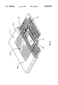
- the thermally enhanced chip carrier package 10 is shown in a cross-sectional, perspective view of the top thereof and is constructed for receipt of one or more suitable semiconductor devices, herein referred to as a chip or die.
- the chip carrier package 10 includes a circuit substrate or board 12 formed of a suitable thermoplastic 14 having a casing 17 formed therearound and a center section cut-out 18A which exposes a heat sink 16 therethrough.
- the substrate 12 is fabricated with a plurality of lead traces 22 extending from the region around a cut-out 18A. Each of the lead traces 22 is located so as to provide electrical isolation from each other and the heat sink 16.
- a secured heat sink and substrate adapted for sealing one or more chips 34 secured thereon from moisture in a reliable and efficient package.
- the assembly described herein has these features and is economical to fabricate.
- a plurality of fragile wires 26 are, in one embodiment, connected between the plurality of inner lead traces 22 and a plurality of electrical connection pads 38 of the chip 34.
- the manufacture of the chip carrier package 10 is accomplished by first producing a circuit substrate 12.
- the circuit substrate 12 may comprise a resinous printed circuit board made of suitable thermoplastic such as polyphenylene sulfate (PPS) or liquid crystal polymer (LCP).
- PPS polyphenylene sulfate
- LCP liquid crystal polymer
- the fabrication of such printed circuit boards is a well established technology and may include multilayer boards having multiple metal layers therein (as discussed below).
- Conventional printed circuit boards have metal patterns on at least one side and often on opposite sides thereof. Some have plated through holes extending between the metal patterns on opposite sides of the board.
- the present invention utilizes metal patterns formed on one or both sides of the board and sometimes within the board through a process of either subtractive or additive etching. Plated through holes may also be formed.
- FIG. 1A shows a pattern 19 on the top side 19A of substrate 12.
- the pattern 19 includes electrical conductive lead traces 22.
- Each one of the plurality of lead traces 22 on top side 19A includes an inner lead trace finger 24, an intermediate trace finger 25 and a plated through hole 28 which extends to a portion of the metal pattern 30 formed on the bottom side 30A of board 12.
- the lead traces 22 are formed during the etching process so that electrical isolation is provided between each one of the plurality of lead traces 22 and portions of pattern 30 (to be discussed below).
- a heat sink mounting ring 20 formed of metal and adapted for solder coating is also formed on the bottom side 30A of substrate 12 in a completely enclosing shape around cut-out 18A so that the heat sink 16 can be solder mounted thereto in sealed engagement therewith.
- FIG. 1B there is shown a perspective view of the bottom side of an alternative embodiment of a thermally enhanced chip carrier cavity package 10A constructed in accordance with the principles of the present invention.
- Package 10A includes a circuit substrate, or board, 12A formed of a suitable thermoplastic 14 having a segmented casing 17A in the form of a resin dam formed around a center cut-out 18A which exposes a heat sink 16 therethrough.
- the substrate 12A is fabricated with a plurality of lead traces 22 extending from the board region around cut-out 18A. Each of the lead traces 22 is located so as to provide electrical isolation from each other and the heat sink 16.
- an advancement over the prior art is provided with regard to the attachment of heat sink 16.
- the heat sink 16 is assembled to the top 19A of the substrate 12A rather than the bottom.
- the heat sink 16 is secured to the top 19A of substrate 12A by a heat sink mounting ring 20 as described above.
- the heat sink mounting ring 20 is formed on the top side 19A of substrate 12A in a generally rectangular shape which surrounds cut-out 18A so that the heat sink 16 can be solder-mounted thereto in a sealed engagement therewith.
- the ring 20 may comprise a metal layer which has been etched thereon.
- the chip 34 is then secured to the heat sink 16 with adhesive, or the like, while fragile wires 26 extend outwardly from connection pads 38 of the chip to inner lead trace fingers 24 of lead traces 22. Unlike FIG.
- the circuit pattern 19 appears only on the bottom side 30A of the substrate 12A with all lead traces 22 extending beneath the segmented casing 17A to electrically connect solder balls 305 to the appropriate connection pad 38.
- Other chip designs such as flip chips, and chip configurations, such as multiple chips in a single board 12A, may be utilized in the package 10A.
- Such chip designs and configurations are more fully set forth in co-pending patent application Ser. No. 08/339,329. It may be seen that in this particular embodiment, the chip 34 and fragile wires 26 are configured for securement within an encapsulant retained by the segmented casing 17A, as will be described in more detail below. As described in FIG.
- this particular configuration also positions the heat sink 16 for the mounting of, and heat dissipation for, the chip 34. Unlike the arrangement of FIG. 1A, however, the chip 34 will be inverted relative to the mounting as the substrate 12A to the appropriate mother board, or the like (not shown).
- FIG. 2 there is shown a method of molding the casing 17 of FIG. 1A over the substrate 12.
- a similar procedure could be used for the casing 17A of FIG. 1B, although other casing forming techniques, such as transfer molding, may also be used.
- the substrate 12 is placed within a molding apparatus 100 adapted for forming the casing 17 thereon.
- the molding apparatus 100 includes a mold housing 102 specifically designed to form casing 17 as shown and for receiving the injection of the suitable thermoplastic 14 onto the circuit substrate 12.
- the casing 17 is molded in a manner which covers a designated region of the circuit substrate 12, often over a plurality of inner lead trace fingers 24, as well as a portion of each one of the plurality of intermediate lead trace portions 25 (see FIG. 1A).
- the suitable thermoplastic 14 is injected so that the casing 17 is formed to define a cavity 18 including, in part, cut-out 18A (see FIGS. 1A, 1B) of substrate 12.
- Cavity 18 then includes a plurality of substantially vertical walls 32 upstanding from the substrate 12. The vertical walls 32 may then function, in part, as a resin dam for encapsulant injected into cavity 18, as described below.
- thermoplastic 14 is in a molten state and is forced through injection ports 104 into mold cavity 105.
- the mold cavity 105 is defined between fixed mold base 107 and moveable platen 109 which together comprise housing 102.
- a venting port 106 is also shown in this particular view.
- the molten state of thermoplastic 14 provides a substantial remelting of the adjacent portion of the top surface 19A of the circuit substrate 12.
- the remelting of the top surface 19A (see FIGS. 1A, 1B) of circuit substrate 12 provides a chemical fusing or bonding of portions of the circuit substrate 12 to the casing 17.
- the fusion then provides a moisture and chemical barrier, substantially equal to that of the suitable thermoplastic 14 itself.
- heat sink 16 may be secured to the substrate 12 and one or more chips 34 may be attached to the heat sink.
- the chip(s) 34 is attached to the heat sink 16 with an adhesive material 35.
- a curing process (as required) is applied to the adhesive material 35 which results in an adhesive mechanical attachment of the chip 34 to the heat sink 16.
- a plurality of fragile wires 26 are connected between the plurality of inner lead trace fingers 22 and a plurality of electrical connection pads 38 of the chip 34.
- the heat sink chip carrier packages 10 and 10A of the present invention may be seen to provide an improved assembly for the mounting of a heat sink to a substrate and the reliable protection of semiconductor devices mounted thereto from the environment.
- What is not shown in FIGS. 1A and 1B is the preferable use of a lid or encapsulant around the semiconductor devices and upon the heat sinks.
- FIG. 3 is a fragmentary perspective of the package of FIG. 1A with an encapsulant 120 filling cavity 18. Portions of the casing 17, substrate 12 and encapsulant 120 are removed (as shown by section lines) for purposes of clarity.
- the casing 17 is disposed upon the substrate 12 around the underlying heat sink 16.
- a mounting ring 20 is utilized for heat sink 16 as described above.
- the casing 17 forms a dam for the encapsulant 120 which is dispensed therein covering the chip 34, heat sink 16, wires 26 and metal pattern 19.
- a lid 122 is disposed over the encapsulant 120 and sealed to the casing 17 as will be described below.
- the following alternative embodiments are also presented for illustrating a variety of packaging approaches in accordance with the principles of the present invention.
- FIG. 4 there is shown the heat sink chip carrier package 10 of FIG. 1A in a fragmentary perspective view thereof with chip 34 secured therein and encapsulated in a liquid encapsulant 52, which may be the same as encapsulant 120 of FIG. 3.
- Mounting ring 20 is also shown securing heat sink 16.
- the liquid encapsulants may vary in type and include RTV, epoxy and silicone, which encapsulants are commonly used today as overcoatings and liquid fills. Because of the presence of casing 17 about the circuit substrate 12, a variety of encapsulation techniques may be utilized for protecting the chip 34, wires 26 and pattern 19 in comparison to other prior art chip carrier cavity packages.
- a lid 130 is recessed within the cavity 18 (formed in part by the casing 17) upon the encapsulant 52 to provide a flush top 132.
- the lid 130 may be separately formed for placement on the encapsulant 52 and securement thereto by a suitable adhesive, including the encapsulant itself.
- the lid 130 may also be formed by injection molding the thermoplastic material directly over the encapsulant 52. This molded lid 130 will then fuse to the casing 17 forming a homogenous surface. Dotted lines 134 are provided to diagrammatically illustrate the intersection between the lid 130 and casing 17. The method of bonding is discussed below.
- FIG. 5 there is shown an alternative embodiment of the liquid encapsulation assembly of FIG. 3 wherein no lid is utilized upon the encapsulant 120.
- a package 299 is thus provided with a variety of advantageous features.
- the chip 34 is protected from the environment by the encapsulant 120 filling the cavity 18 within the casing 17 and further bonded to the substrate 12 and the heat sink 16 over wires 26.
- a variety of combinations of material and/or bonding techniques may be utilized in accordance with the principles of the present invention as described below.
- FIG. 6 there is shown an alternative embodiment of portions of a heat sink carrier package constructed in accordance with the principles of the present invention.
- a segmented casing 217 in the form of the segmented casing 17A of FIG. 1B is shown and secured to the top side 19A of circuit substrate 12 of a heat sink chip carrier package 220.
- the segmented casing 217 is much smaller, and particularly narrower than the casing 17 of FIG. 1A and covers a lesser portion of the metal pattern 19.
- the inside walls 222 of casing 217 are positioned in approximately the same location as the inside walls of casing 17 of FIG. 1A relative to the substrate 12.
- the outside walls 224 are recessed inwardly from the perimeter 226 of substrate 12.
- outer portions 228 of pattern 19 are exposed after assembly of a heat sink, a chip and an encapsulant (none of which being shown for purposes of clarity) to the substrate 12.
- the encapsutant may, as described above, be dispensed into the cavity 18 and contained by the inside walls 222.
- One advantage of this particular embodiment is the fact that the casing 217 of package 220 may be strip molded, which technique is conventional in the industry. Another advantage is that the casing 217 requires less material volume and the associated expense of the thermoplastic material used to form said casing. If a thermoplastic material such as PPS or LCP is used for the substrate 12 and casing 217, said casing may be chemically fused to the substrate 12 during the injection molding process.
- FIG. 7 there is shown a diagrammatic, side-elevational, cross-sectional view of an alternative embodiment of a heat sink carrier package constructed in accordance with the principles of the present invention.
- a conventional chip 34 is secured to a heat sink 16 secured to the bottomside 30A of substrate 12 (as shown in FIG. 1A) to form gas tight lid seal package 300.
- lid 54 is secured atop the casing 17 in a "gas tight" configuration without the presence of a liquid encapsulant therein.
- the gas tight lid seal may be provided by a variety of techniques as described below.
- One of the techniques, in accordance with the principles of the present invention, is to fabricate the lid 54 from the same thermoplastic from which the casing 17 is formed whereby the lid 54 may be chemically fused to the casing 17 by utilizing heat or the like.
- FIG. 8 there is shown yet an alternative embodiment of the securement of a chip 34 to a substrate 12 in accordance with the principles of the present invention.
- a cup seal lid 60 is provided having side walls 62 of a width substantially equivalent to the width of the side walls of the casing 17 as shown in FIG. 7.
- the bonding of the cup seal lid 60 to the top surface of the substrate 12 may be affected by heat or the like to form a chemical fusion therebetween and provide the advantageous results described above for protecting the chip 34 therein.
- FIG. 9 there is shown an enlarged, side-elevational, cross sectional view of a portion of the casing 17 and substrate 12 of the heat sink chip carrier cavity package 10 of FIG. 1A.
- the plated through holes 28 establish the electrical connection between the circuit pattern 19 on the top side 19A and the circuit pattern 30 on the bottom side 30A of substrate 12. Plated through holes may not be required with the embodiment of FIG. 1B. It may be seen that by utilizing a common thermoplastic material in both embodiments, the adherence of the casing 17 to the substrate 12 effectively eliminates any possibility of moisture infiltration into a chip mounted on the heat sink 16.
- substrate 12 is fabricated with metal patterns 19 and 30, first portions of which being electrically connected by plated through holes 28 and second portions of which being covered with a mask 301.
- a series of land areas 303 are provided for electrical interconnection to the carrier package 10.
- the heat sink 16 is shown to be mounted to the underside 30A of substrate 12 through mounting ring 20, which is part of metal surface pattern 302 that permits the heat sink 16 to be directly soldered to the substrate 12.
- the use of a separate surface pattern 302 (of which mounting ring 20 is a part) enables the heat sink 16 to be secured to the substrate 12 without the use of adhesives or the like.
- This securement technique also provides enhanced moisture resistance to the assembly, because adhesives, such as epoxy, absorb moisture and allow quicker penetration of moisture into the cavity 18.
- adhesives such as epoxy
- adhesives absorb moisture and allow quicker penetration of moisture into the cavity 18.
- adhesives which could otherwise be used to bond the heat sink. For example, adhesives often bleed into unwanted areas during application. Additionally, adhesives have limited temperature capacity and may not meet the temperature requirements of further processing such as soldering.
- FIG. 10 there is shown an alternative embodiment of the assembly of FIG. 9.
- the casing 17 surrounding cavity 18 with chip 34 secured therein on heat sink 16 is further enhanced by a series of solder balls 305 secured to the land areas 303 of substrate 12. Electrical connection to the solder balls 305 is provided from the wires 26 connected to pattern 19 of top side 19A, through the plated through hole 28 and across the pattern 30 of side 30A.
- the land areas 303 are part of pattern 30 and afford a useful electrical connection system.
- Mounting ring 20 is again shown securing heat sink 16 to the substrate 12.
- FIG. 11 there is shown an enlarged, side-elevational, cross sectional view of an alternative embodiment of the package 300 of FIG. 7.
- heat sink 16 is secured to substrate 12 by mounting ring 20.
- Solder balls 305 have been attached to the land areas 303 described in FIGS. 9 and 10.
- Lid 54 has been secured to the casing 17 to create a gas tight seal.
- a preferable method of securement is fabricating both the casing 17 and lid 54 of the same thermoplastic material and applying sufficient heat for chemical fusion. The use of other adhesives could also be included.
- FIG. 12 there is shown an enlarged, side-elevational, cross sectional view of the package 299 of FIG. 5 with solder balls 305 depending from surface 30A.
- Encapsulant 120 is shown filling the cavity 18 to the top of casing 17.
- the wires 26 are protected from the environment by the encapsulant 120.
- the manner of filling cavities with encapsulants is conventional in the art and further description is not deemed necessary.
- FIG. 13 there is shown an enlarged side-elevational, cross sectional view of the package 10 of FIG. 3 with solder balls 305 depending from surface 30A.
- the lid 122 extends over encapsulant 120 and is bonded to the top of casing 17.
- the lid 122 may be bonded as described above in FIG. 12. It may be seen in this view and FIG. 12 that the solder balls 305 are not disposed over the plated through hole 28.
- solder balls 305 are formed over and attached to the bottom side of plated through holes 28. All solder balls 305 of this particular illustration are deployed inwardly of casing 17, although this may not always be preferable.
- FIG. 15A there is shown a perspective view of the bottom 30A of the substrate 12 of FIG. 1A illustrating the securement of the heat sink 16 thereto.
- the heat sink 16 is secured to the bottom 30A of substrate 12 by mounting ring 20.
- the mounting ring 20 is formed of metal on substrate 12 outwardly of cavity 18 and provides means for securing said heat sink 16 thereto.
- solder preform 20A above amounting ring 20.
- the solder preform 20A is shown in position for application to the metal mounting ring 20 and comprises but one of a variety of techniques for applying solder for securement of the heat sink 16 to the substrate 12.
- the utilization of solder preforms 20A may, in certain applications, be preferable because the preform shape can be specifically created, aligned and placed upon the mounting ring 20 with appropriate alignment fixtures (not shown).
- Other solder application techniques also exist in accordance with existing industry standards. For example, solder may be dispensed upon the mounting ring 20 in a paste form by a syringe or the like. Solder may also be applied through a silk screen onto the mounting ring 20.
- FIG. 15B there is shown the substrate 12 of FIG. 15A before the heat sink 16 is applied.
- the mounting ring 20 is more completely shown and may be seen to comprise an enlarged region surrounding the cut-out 18A.
- the mounting ring 20 As discussed above, only the mounting ring 20, solder, and standard soldering procedures are required for attachment of heat sink 16 to the substrate. In this view, the solder 20B has been applied to the ring 20.
- the assembly is now ready for positioning of the heat sink 16 (shown in FIG. 15A).
- the outer periphery of mounting ring 20 is shown around the solder 20B.
- FIG. 16A there is shown an enlarged, side-elevational, cross-sectional view of the package 10A of FIG. 1B.
- the top 19A of substrate 12A has secured thereon the heat sink 16 while the bottom 30A has depending therefrom solder balls 305.
- the mounting ring 20 is clearly shown securing said heat sink 16 to said substrate 12A.
- the chip 34 is downwardly oriented from the heat sink 16 and fragile wires 26 extend from the chip 34 to the circuit pattern 19 formed on side 30A.
- Segmented casing 17A likewise extends from substrate 12A around the wires 26.
- the circuit pattern 19 provides interconnection between the fragile wires 26 extending from chip 34 to the select solder ball 305 providing appropriate electrical interconnection therewith.
- FIG. 16B there is shown a side-elevational, cross-sectional view of the package 10A of FIG. 16A illustrating one encapsulation configuration thereof.
- an encapsulant 120A has been applied within the segmented casing 17A for protection and sealing of the chip 34 and fragile wires 26 extending therefrom.
- This particular encapsulation configuration is but one illustration of the principles of the present invention as utilized in a downwardly oriented chip configuration. A variety of lids, encapsulants and sealing techniques can be used, and these are described above for the package 10.
- FIG. 17A there is shown a side-elevational, cross-sectional view of a chip carrier package 410 comprising an alternative embodiment of the package 10 of FIG. 16A.
- Package 410 comprises a multilayer substrate 412 formed with multiple metal layers, a top loaded heat sink 16, and a downwardly extending casing 417 surrounding around a chip 34.
- Multilayer substrate 412 as shown in this view thus includes metal layers 414 and 416 disposed between the top and bottom surfaces 418 and 420, respectively, of the substrate 412. Layers of the substrate 412 separate each of the aforesaid metal layers.
- the substrate layers include the suitable thermoplastic such as PPS or LCP in combination with the appropriate reinforcing mat such as glass fibers.
- Plated-through holes such as plated-through holes 422 and 424 are shown to interconnect select ones of the metal layers 414 and 416.
- the fabrication of a multilayer board is conventional in the art.
- the present invention is directed to the utilization of a mounting technique for a heat sink 16 in association with such a substrate assembly.
- FIG. 17B there is shown a side-elevational, cross-sectional view of the package 410 comprising an alternative embodiment of the package 10A of FIG. 16B with encapsulant 430 molded over chip 34.
- Casing 417 depends from the bottom surface 420 of the substrate 412 while providing a means for containing the encapsulant 430 therein.
- lids and other sealant configurations are contemplated by the present invention in accordance with the discussions set forth above.
- the present invention utilizes a heat sink 16 to form a thermally enhanced chip carrier package in a variety of configurations.
- a wide assortment of encapsulants and lid assemblies may be utilized in accordance with the principles of the present invention. It is preferable in one embodiment to use a common homogeneous material for the fabrication of casings 17 and 17A and substrates 12 and 12A as well as the lid 54. Other combinations of materials may be used.
- Lid 54 may, for example, be metal and a specific adhesive may be utilized for bonding the casings 17 and 17A to the lid 54.
Abstract
Description
Claims (31)
Priority Applications (1)
| Application Number | Priority Date | Filing Date | Title |
|---|---|---|---|
| US08/383,966 US5650593A (en) | 1994-05-26 | 1995-02-06 | Thermally enhanced chip carrier package |
Applications Claiming Priority (3)
| Application Number | Priority Date | Filing Date | Title |
|---|---|---|---|
| US08/250,153 US5471011A (en) | 1994-05-26 | 1994-05-26 | Homogeneous thermoplastic semi-conductor chip carrier package |
| US08/339,329 US5827999A (en) | 1994-05-26 | 1994-11-14 | Homogeneous chip carrier package |
| US08/383,966 US5650593A (en) | 1994-05-26 | 1995-02-06 | Thermally enhanced chip carrier package |
Related Parent Applications (1)
| Application Number | Title | Priority Date | Filing Date |
|---|---|---|---|
| US08/339,329 Continuation-In-Part US5827999A (en) | 1994-05-26 | 1994-11-14 | Homogeneous chip carrier package |
Publications (1)
| Publication Number | Publication Date |
|---|---|
| US5650593A true US5650593A (en) | 1997-07-22 |
Family
ID=26940637
Family Applications (1)
| Application Number | Title | Priority Date | Filing Date |
|---|---|---|---|
| US08/383,966 Expired - Lifetime US5650593A (en) | 1994-05-26 | 1995-02-06 | Thermally enhanced chip carrier package |
Country Status (1)
| Country | Link |
|---|---|
| US (1) | US5650593A (en) |
Cited By (68)
| Publication number | Priority date | Publication date | Assignee | Title |
|---|---|---|---|---|
| US5784260A (en) * | 1996-05-29 | 1998-07-21 | International Business Machines Corporation | Structure for constraining the flow of encapsulant applied to an I/C chip on a substrate |
| GB2321339A (en) * | 1997-01-16 | 1998-07-22 | Nec Corp | External connections for semiconductor chips |
| US5814894A (en) * | 1995-04-07 | 1998-09-29 | Nitto Denko Corporation | Semiconductor device, production method thereof, and tape carrier for semiconductor device used for producing the semiconductor device |
| US5847445A (en) * | 1996-11-04 | 1998-12-08 | Micron Technology, Inc. | Die assemblies using suspended bond wires, carrier substrates and dice having wire suspension structures, and methods of fabricating same |
| WO1998059368A1 (en) * | 1997-06-20 | 1998-12-30 | Substrate Technologies, Inc. | Sequentially built integrated circuit package |
| US5994773A (en) * | 1996-03-06 | 1999-11-30 | Hirakawa; Tadashi | Ball grid array semiconductor package |
| US6084298A (en) * | 1995-03-10 | 2000-07-04 | Nec Corporation | Manufacturing of semiconductor device |
| US6120301A (en) * | 1995-08-17 | 2000-09-19 | Hitachi, Ltd. | Semiconductor device and method of manufacturing the same |
| US6121553A (en) * | 1997-03-03 | 2000-09-19 | Hitachi Chemical Company, Ltd. | Circuit boards using heat resistant resin for adhesive layers |
| US6127194A (en) * | 1998-12-09 | 2000-10-03 | Advanced Micro Devices, Inc. | Package removal for FBGA devices |
| US6129260A (en) * | 1998-08-19 | 2000-10-10 | Fravillig Technologies Company | Solderable structures |
| US6140707A (en) * | 1998-05-07 | 2000-10-31 | 3M Innovative Properties Co. | Laminated integrated circuit package |
| US6214650B1 (en) | 2000-02-01 | 2001-04-10 | Lockheed Martin Corporation | Method and apparatus for sealing a ball grid array package and circuit card interconnection |
| US6252298B1 (en) * | 1997-06-18 | 2001-06-26 | Samsung Electronics Co., Ltd. | Semiconductor chip package using flexible circuit board with central opening |
| US6278178B1 (en) * | 1998-02-10 | 2001-08-21 | Hyundai Electronics Industries Co., Ltd. | Integrated device package and fabrication methods thereof |
| US6281580B1 (en) * | 1998-08-11 | 2001-08-28 | Fujitsu Limited | LSI package and inner lead wiring method for same |
| US6291263B1 (en) * | 2000-06-13 | 2001-09-18 | Siliconware Precision Industries Co., Ltd. | Method of fabricating an integrated circuit package having a core-hollowed encapsulation body |
| US6329220B1 (en) * | 1999-11-23 | 2001-12-11 | Micron Technology, Inc. | Packages for semiconductor die |
| US6337228B1 (en) | 1999-05-12 | 2002-01-08 | Amkor Technology, Inc. | Low-cost printed circuit board with integral heat sink for semiconductor package |
| US6372540B1 (en) * | 2000-04-27 | 2002-04-16 | Amkor Technology, Inc. | Moisture-resistant integrated circuit chip package and method |
| US6407458B1 (en) | 2000-05-04 | 2002-06-18 | Amkor Technology, Inc. | Moisture-resistant integrated circuit chip package and method |
| US6414396B1 (en) | 2000-01-24 | 2002-07-02 | Amkor Technology, Inc. | Package for stacked integrated circuits |
| US6429513B1 (en) | 2001-05-25 | 2002-08-06 | Amkor Technology, Inc. | Active heat sink for cooling a semiconductor chip |
| US6448509B1 (en) | 2000-02-16 | 2002-09-10 | Amkor Technology, Inc. | Printed circuit board with heat spreader and method of making |
| US6462274B1 (en) | 1998-10-31 | 2002-10-08 | Amkor Technology, Inc. | Chip-scale semiconductor package of the fan-out type and method of manufacturing such packages |
| US6476331B1 (en) | 2000-06-19 | 2002-11-05 | Amkor Technology, Inc. | Printed circuit board for semiconductor package and method for manufacturing the same |
| US20020187590A1 (en) * | 2000-08-31 | 2002-12-12 | Micron Technology, Inc. | Ball grid array packages with thermally conductive containers |
| US6509642B1 (en) * | 2000-07-28 | 2003-01-21 | Agere Systems Inc. | Integrated circuit package |
| US6518088B1 (en) * | 1994-09-23 | 2003-02-11 | Siemens N.V. And Interuniversitair Micro-Electronica Centrum Vzw | Polymer stud grid array |
| US20030064542A1 (en) * | 2001-10-02 | 2003-04-03 | Corisis David J. | Methods of packaging an integrated circuit |
| US20030068840A1 (en) * | 2000-04-28 | 2003-04-10 | Grigg Ford B. | Interposers including upwardly protruding dams, semiconductor device assemblies including the interposers, and methods |
| US20030155636A1 (en) * | 2002-02-15 | 2003-08-21 | Cobbley Chad A. | Molded stiffener for thin substrates |
| US20030178719A1 (en) * | 2002-03-22 | 2003-09-25 | Combs Edward G. | Enhanced thermal dissipation integrated circuit package and method of manufacturing enhanced thermal dissipation integrated circuit package |
| US20040012083A1 (en) * | 2002-06-19 | 2004-01-22 | Brian Farrell | Electronic and optoelectronic component packaging technique |
| US6683386B2 (en) * | 2000-10-11 | 2004-01-27 | United Test Center, Inc. | Low profile optically-sensitive semiconductor package |
| US6686226B1 (en) * | 1994-02-10 | 2004-02-03 | Hitachi, Ltd. | Method of manufacturing a semiconductor device a ball grid array package structure using a supporting frame |
| US20040045158A1 (en) * | 2000-02-08 | 2004-03-11 | Cardiac Pacemakers, Inc. | Thin film deposition as an active conductor and method therefor |
| US6713856B2 (en) * | 2002-09-03 | 2004-03-30 | Ultratera Corporation | Stacked chip package with enhanced thermal conductivity |
| US6734552B2 (en) | 2001-07-11 | 2004-05-11 | Asat Limited | Enhanced thermal dissipation integrated circuit package |
| US20040120129A1 (en) * | 2002-12-24 | 2004-06-24 | Louis Soto | Multi-layer laminated structures for mounting electrical devices and method for fabricating such structures |
| US20040120120A1 (en) * | 2002-12-24 | 2004-06-24 | Louis Soto | Multi-layer laminated structures, method for fabricating such structures, and power supply including such structures |
| US20040125568A1 (en) * | 2002-12-30 | 2004-07-01 | Advanced Semiconductor Engineering, Inc. | Thermal enhance package and manufacturing method thereof |
| US20040155360A1 (en) * | 1999-09-02 | 2004-08-12 | Salman Akram | Board-on-chip packages |
| US20040164411A1 (en) * | 1999-05-07 | 2004-08-26 | Amkor Technology, Inc. | Semiconductor package and method for fabricating the same |
| US20040175916A1 (en) * | 1999-05-20 | 2004-09-09 | Amkor Technology, Inc. | Stackable semiconductor package having semiconductor chip within central through hole of substrate |
| US20040207060A1 (en) * | 1999-02-19 | 2004-10-21 | Corisis David J. | Integrated circuit packages, ball-grid array integrated circuit packages and methods of packaging an integrated circuit |
| US20050047106A1 (en) * | 2003-08-29 | 2005-03-03 | Martino Peter Miguel | Substrate reinforcing in an LGA package |
| US6919631B1 (en) | 2001-12-07 | 2005-07-19 | Amkor Technology, Inc. | Structures for improving heat dissipation in stacked semiconductor packages |
| US20050212122A1 (en) * | 2004-03-25 | 2005-09-29 | Duggan Michael R | Multi-layer fet array and method of fabricating |
| US20050275081A1 (en) * | 2004-06-12 | 2005-12-15 | Roger Chang | Embedded chip semiconductor having dual electronic connection faces |
| US7015072B2 (en) | 2001-07-11 | 2006-03-21 | Asat Limited | Method of manufacturing an enhanced thermal dissipation integrated circuit package |
| US20060068527A1 (en) * | 2004-09-02 | 2006-03-30 | Micron Technology Inc. | Molded stiffener for thin substrates |
| US20060268645A1 (en) * | 2005-05-27 | 2006-11-30 | Alfons Graf | Protection Circuit |
| US20070107932A1 (en) * | 2005-11-09 | 2007-05-17 | Jauniskis Linas A | Moisture resistant chip package |
| US20070145548A1 (en) * | 2003-12-22 | 2007-06-28 | Amkor Technology, Inc. | Stack-type semiconductor package and manufacturing method thereof |
| US20070159803A1 (en) * | 2006-01-09 | 2007-07-12 | Honeywell International, Inc. | MEMS device seal using liquid crystal polymer |
| US20070246841A1 (en) * | 2006-04-19 | 2007-10-25 | Nichia Corporation | Semiconductor device |
| USRE40112E1 (en) | 1999-05-20 | 2008-02-26 | Amkor Technology, Inc. | Semiconductor package and method for fabricating the same |
| US20100012354A1 (en) * | 2008-07-14 | 2010-01-21 | Logan Brook Hedin | Thermally conductive polymer based printed circuit board |
| USRE41722E1 (en) * | 1994-12-20 | 2010-09-21 | Renesas Electronics Corp. | Semiconductor device having an improved connection arrangement between a semiconductor pellet and base substrate electrodes and a method of manufacture thereof |
| US20130269183A1 (en) * | 2012-03-28 | 2013-10-17 | Ttm Technologies, Inc. | Printed circuit board interconnect assembly and method |
| WO2016030067A1 (en) * | 2014-08-29 | 2016-03-03 | Robert Bosch Gmbh | Module assembly and transmission control module |
| US20160081197A1 (en) * | 2014-09-12 | 2016-03-17 | International Business Machines Corporation | Compute intensive module packaging |
| US20160157359A1 (en) * | 2014-11-07 | 2016-06-02 | International Business Machines Corporation | Customized module lid |
| US9466545B1 (en) | 2007-02-21 | 2016-10-11 | Amkor Technology, Inc. | Semiconductor package in package |
| CN111696927A (en) * | 2020-05-18 | 2020-09-22 | 马鞍山芯海科技有限公司 | Chip packaging frame and chip packaging method |
| WO2021208322A1 (en) * | 2020-04-13 | 2021-10-21 | 烽火通信科技股份有限公司 | Multi-chip heat-dissipating packaging structure and packaging method |
| US11587839B2 (en) * | 2019-06-27 | 2023-02-21 | Analog Devices, Inc. | Device with chemical reaction chamber |
Citations (48)
| Publication number | Priority date | Publication date | Assignee | Title |
|---|---|---|---|---|
| US3644798A (en) * | 1969-06-16 | 1972-02-22 | Hitachi Ltd | High-power integrated circuit ceramic package with metallic heat-conducting body |
| US3790859A (en) * | 1970-02-19 | 1974-02-05 | Texas Instruments Inc | Electronic package header system having omni-directional heat dissipation characteristic |
| US3867759A (en) * | 1973-06-13 | 1975-02-25 | Us Air Force | Method of manufacturing a multi-layered strip transmission line printed circuit board integrated package |
| USRE29325E (en) * | 1971-01-26 | 1977-07-26 | Minnesota Mining And Manufacturing Company | Hermetic power package |
| US4195193A (en) * | 1979-02-23 | 1980-03-25 | Amp Incorporated | Lead frame and chip carrier housing |
| JPS57194556A (en) * | 1981-05-26 | 1982-11-30 | Toshiba Corp | Heat radiating package |
| JPS59188948A (en) * | 1983-04-11 | 1984-10-26 | Nec Corp | Chip carrier |
| US4480262A (en) * | 1982-07-15 | 1984-10-30 | Olin Corporation | Semiconductor casing |
| US4507907A (en) * | 1981-09-02 | 1985-04-02 | Burr-Brown Corporation | Expendable heater sealing process |
| US4509096A (en) * | 1983-02-22 | 1985-04-02 | Smiths Industries Public Limited Company | Chip-carrier substrates |
| US4521801A (en) * | 1981-10-09 | 1985-06-04 | Tokyo Shibaura Denki Kabushiki Kaisha | Semiconductor device with composite lead wire |
| JPS60127747A (en) * | 1983-12-15 | 1985-07-08 | Matsushita Electric Ind Co Ltd | Resin-sealed semiconductor device |
| JPS60198818A (en) * | 1984-03-23 | 1985-10-08 | Nec Corp | Photoresist developing device |
| JPS61114563A (en) * | 1984-11-09 | 1986-06-02 | Nec Corp | Integrated circuit package |
| US4630172A (en) * | 1983-03-09 | 1986-12-16 | Printed Circuits International | Semiconductor chip carrier package with a heat sink |
| JPS6281735A (en) * | 1985-10-04 | 1987-04-15 | Sumitomo Electric Ind Ltd | Package integral with radiator fin |
| US4700276A (en) * | 1986-01-03 | 1987-10-13 | Motorola Inc. | Ultra high density pad array chip carrier |
| US4823234A (en) * | 1985-08-16 | 1989-04-18 | Dai-Ichi Seiko Co., Ltd. | Semiconductor device and its manufacture |
| US4843695A (en) * | 1987-07-16 | 1989-07-04 | Digital Equipment Corporation | Method of assembling tab bonded semiconductor chip package |
| US4868349A (en) * | 1988-05-09 | 1989-09-19 | National Semiconductor Corporation | Plastic molded pin-grid-array power package |
| US4876588A (en) * | 1987-09-16 | 1989-10-24 | Nec Corporation | Semiconductor device having ceramic package incorporated with a heat-radiator |
| US4878108A (en) * | 1987-06-15 | 1989-10-31 | International Business Machines Corporation | Heat dissipation package for integrated circuits |
| US4887149A (en) * | 1986-07-17 | 1989-12-12 | Sgs Microelectronica S.P.A. | Semiconductor device mounted in a highly flexible, segmented package, provided with heat sink |
| US4890152A (en) * | 1986-02-14 | 1989-12-26 | Matsushita Electric Works, Ltd. | Plastic molded chip carrier package and method of fabricating the same |
| JPH027545A (en) * | 1988-06-27 | 1990-01-11 | Nec Corp | Container for semiconductor device |
| US4894709A (en) * | 1988-03-09 | 1990-01-16 | Massachusetts Institute Of Technology | Forced-convection, liquid-cooled, microchannel heat sinks |
| US4910583A (en) * | 1987-06-04 | 1990-03-20 | Licentia Patent-Verwaltungs Gmbh | Semiconductor body with heat sink |
| US4940181A (en) * | 1989-04-06 | 1990-07-10 | Motorola, Inc. | Pad grid array for receiving a solder bumped chip carrier |
| US4965660A (en) * | 1983-09-22 | 1990-10-23 | Hitachi, Ltd. | Integrated circuit package having heat sink bonded with resinous adhesive |
| US4978638A (en) * | 1989-12-21 | 1990-12-18 | International Business Machines Corporation | Method for attaching heat sink to plastic packaged electronic component |
| US5006673A (en) * | 1989-12-07 | 1991-04-09 | Motorola, Inc. | Fabrication of pad array carriers from a universal interconnect structure |
| US5027191A (en) * | 1989-05-11 | 1991-06-25 | Westinghouse Electric Corp. | Cavity-down chip carrier with pad grid array |
| JPH03261165A (en) * | 1990-03-12 | 1991-11-21 | Hitachi Ltd | Semiconductor device |
| JPH04142068A (en) * | 1990-10-01 | 1992-05-15 | Ibiden Co Ltd | Electronical component mounting board and manufacture thereof |
| US5152057A (en) * | 1987-11-17 | 1992-10-06 | Mold-Pac Corporation | Molded integrated circuit package |
| US5155579A (en) * | 1991-02-05 | 1992-10-13 | Advanced Micro Devices | Molded heat sink for integrated circuit package |
| US5194695A (en) * | 1990-11-02 | 1993-03-16 | Ak Technology, Inc. | Thermoplastic semiconductor package |
| US5241133A (en) * | 1990-12-21 | 1993-08-31 | Motorola, Inc. | Leadless pad array chip carrier |
| US5254500A (en) * | 1991-02-05 | 1993-10-19 | Advanced Micro Devices, Inc. | Method for making an integrally molded semiconductor device heat sink |
| US5278446A (en) * | 1992-07-06 | 1994-01-11 | Motorola, Inc. | Reduced stress plastic package |
| US5293301A (en) * | 1990-11-30 | 1994-03-08 | Shinko Electric Industries Co., Ltd. | Semiconductor device and lead frame used therein |
| JPH06148950A (en) * | 1992-11-09 | 1994-05-27 | Mitsubishi Kasei Corp | Carrier and developer for electrostatic charge image developing |
| US5328870A (en) * | 1992-01-17 | 1994-07-12 | Amkor Electronics, Inc. | Method for forming plastic molded package with heat sink for integrated circuit devices |
| US5345106A (en) * | 1990-06-01 | 1994-09-06 | Robert Bosch Gmbh | Electronic circuit component with heat sink mounted on a lead frame |
| US5355283A (en) * | 1993-04-14 | 1994-10-11 | Amkor Electronics, Inc. | Ball grid array with via interconnection |
| US5357673A (en) * | 1991-08-26 | 1994-10-25 | Motorola, Inc. | Semiconductor device encapsulation method |
| US5371404A (en) * | 1993-02-04 | 1994-12-06 | Motorola, Inc. | Thermally conductive integrated circuit package with radio frequency shielding |
| US5378869A (en) * | 1992-06-02 | 1995-01-03 | Amkor Electronics, Inc. | Method for forming an integrated circuit package with via interconnection |
-
1995
- 1995-02-06 US US08/383,966 patent/US5650593A/en not_active Expired - Lifetime
Patent Citations (48)
| Publication number | Priority date | Publication date | Assignee | Title |
|---|---|---|---|---|
| US3644798A (en) * | 1969-06-16 | 1972-02-22 | Hitachi Ltd | High-power integrated circuit ceramic package with metallic heat-conducting body |
| US3790859A (en) * | 1970-02-19 | 1974-02-05 | Texas Instruments Inc | Electronic package header system having omni-directional heat dissipation characteristic |
| USRE29325E (en) * | 1971-01-26 | 1977-07-26 | Minnesota Mining And Manufacturing Company | Hermetic power package |
| US3867759A (en) * | 1973-06-13 | 1975-02-25 | Us Air Force | Method of manufacturing a multi-layered strip transmission line printed circuit board integrated package |
| US4195193A (en) * | 1979-02-23 | 1980-03-25 | Amp Incorporated | Lead frame and chip carrier housing |
| JPS57194556A (en) * | 1981-05-26 | 1982-11-30 | Toshiba Corp | Heat radiating package |
| US4507907A (en) * | 1981-09-02 | 1985-04-02 | Burr-Brown Corporation | Expendable heater sealing process |
| US4521801A (en) * | 1981-10-09 | 1985-06-04 | Tokyo Shibaura Denki Kabushiki Kaisha | Semiconductor device with composite lead wire |
| US4480262A (en) * | 1982-07-15 | 1984-10-30 | Olin Corporation | Semiconductor casing |
| US4509096A (en) * | 1983-02-22 | 1985-04-02 | Smiths Industries Public Limited Company | Chip-carrier substrates |
| US4630172A (en) * | 1983-03-09 | 1986-12-16 | Printed Circuits International | Semiconductor chip carrier package with a heat sink |
| JPS59188948A (en) * | 1983-04-11 | 1984-10-26 | Nec Corp | Chip carrier |
| US4965660A (en) * | 1983-09-22 | 1990-10-23 | Hitachi, Ltd. | Integrated circuit package having heat sink bonded with resinous adhesive |
| JPS60127747A (en) * | 1983-12-15 | 1985-07-08 | Matsushita Electric Ind Co Ltd | Resin-sealed semiconductor device |
| JPS60198818A (en) * | 1984-03-23 | 1985-10-08 | Nec Corp | Photoresist developing device |
| JPS61114563A (en) * | 1984-11-09 | 1986-06-02 | Nec Corp | Integrated circuit package |
| US4823234A (en) * | 1985-08-16 | 1989-04-18 | Dai-Ichi Seiko Co., Ltd. | Semiconductor device and its manufacture |
| JPS6281735A (en) * | 1985-10-04 | 1987-04-15 | Sumitomo Electric Ind Ltd | Package integral with radiator fin |
| US4700276A (en) * | 1986-01-03 | 1987-10-13 | Motorola Inc. | Ultra high density pad array chip carrier |
| US4890152A (en) * | 1986-02-14 | 1989-12-26 | Matsushita Electric Works, Ltd. | Plastic molded chip carrier package and method of fabricating the same |
| US4887149A (en) * | 1986-07-17 | 1989-12-12 | Sgs Microelectronica S.P.A. | Semiconductor device mounted in a highly flexible, segmented package, provided with heat sink |
| US4910583A (en) * | 1987-06-04 | 1990-03-20 | Licentia Patent-Verwaltungs Gmbh | Semiconductor body with heat sink |
| US4878108A (en) * | 1987-06-15 | 1989-10-31 | International Business Machines Corporation | Heat dissipation package for integrated circuits |
| US4843695A (en) * | 1987-07-16 | 1989-07-04 | Digital Equipment Corporation | Method of assembling tab bonded semiconductor chip package |
| US4876588A (en) * | 1987-09-16 | 1989-10-24 | Nec Corporation | Semiconductor device having ceramic package incorporated with a heat-radiator |
| US5152057A (en) * | 1987-11-17 | 1992-10-06 | Mold-Pac Corporation | Molded integrated circuit package |
| US4894709A (en) * | 1988-03-09 | 1990-01-16 | Massachusetts Institute Of Technology | Forced-convection, liquid-cooled, microchannel heat sinks |
| US4868349A (en) * | 1988-05-09 | 1989-09-19 | National Semiconductor Corporation | Plastic molded pin-grid-array power package |
| JPH027545A (en) * | 1988-06-27 | 1990-01-11 | Nec Corp | Container for semiconductor device |
| US4940181A (en) * | 1989-04-06 | 1990-07-10 | Motorola, Inc. | Pad grid array for receiving a solder bumped chip carrier |
| US5027191A (en) * | 1989-05-11 | 1991-06-25 | Westinghouse Electric Corp. | Cavity-down chip carrier with pad grid array |
| US5006673A (en) * | 1989-12-07 | 1991-04-09 | Motorola, Inc. | Fabrication of pad array carriers from a universal interconnect structure |
| US4978638A (en) * | 1989-12-21 | 1990-12-18 | International Business Machines Corporation | Method for attaching heat sink to plastic packaged electronic component |
| JPH03261165A (en) * | 1990-03-12 | 1991-11-21 | Hitachi Ltd | Semiconductor device |
| US5345106A (en) * | 1990-06-01 | 1994-09-06 | Robert Bosch Gmbh | Electronic circuit component with heat sink mounted on a lead frame |
| JPH04142068A (en) * | 1990-10-01 | 1992-05-15 | Ibiden Co Ltd | Electronical component mounting board and manufacture thereof |
| US5194695A (en) * | 1990-11-02 | 1993-03-16 | Ak Technology, Inc. | Thermoplastic semiconductor package |
| US5293301A (en) * | 1990-11-30 | 1994-03-08 | Shinko Electric Industries Co., Ltd. | Semiconductor device and lead frame used therein |
| US5241133A (en) * | 1990-12-21 | 1993-08-31 | Motorola, Inc. | Leadless pad array chip carrier |
| US5254500A (en) * | 1991-02-05 | 1993-10-19 | Advanced Micro Devices, Inc. | Method for making an integrally molded semiconductor device heat sink |
| US5155579A (en) * | 1991-02-05 | 1992-10-13 | Advanced Micro Devices | Molded heat sink for integrated circuit package |
| US5357673A (en) * | 1991-08-26 | 1994-10-25 | Motorola, Inc. | Semiconductor device encapsulation method |
| US5328870A (en) * | 1992-01-17 | 1994-07-12 | Amkor Electronics, Inc. | Method for forming plastic molded package with heat sink for integrated circuit devices |
| US5378869A (en) * | 1992-06-02 | 1995-01-03 | Amkor Electronics, Inc. | Method for forming an integrated circuit package with via interconnection |
| US5278446A (en) * | 1992-07-06 | 1994-01-11 | Motorola, Inc. | Reduced stress plastic package |
| JPH06148950A (en) * | 1992-11-09 | 1994-05-27 | Mitsubishi Kasei Corp | Carrier and developer for electrostatic charge image developing |
| US5371404A (en) * | 1993-02-04 | 1994-12-06 | Motorola, Inc. | Thermally conductive integrated circuit package with radio frequency shielding |
| US5355283A (en) * | 1993-04-14 | 1994-10-11 | Amkor Electronics, Inc. | Ball grid array with via interconnection |
Non-Patent Citations (4)
| Title |
|---|
| E. Berndlmaier & J.A. Dorler / Semiconductor Package with Improved Cooling / IBM Corporation / Feb. 1978 / vol. 20, No. 2. * |
| E. Berndlmaier & J.A. Dorler / Semiconductor Package with Improved Cooling/ IBM Corporation / Feb. 1978 / vol. 20, No. 2. |
| Q.K. Kerjilian & G.C. Phillips, Jr./ Thermally Enhanced Multi layer Ceramic Substrate Structure / IBM Corporation/Jul. 1975/ vol. 18, No. 2. * |
| Q.K. Kerjilian & G.C. Phillips, Jr./ Thermally Enhanced Multi layer Ceramic Substrate Structure/ IBM Corporation/Jul. 1975/ vol. 18, No. 2. |
Cited By (126)
| Publication number | Priority date | Publication date | Assignee | Title |
|---|---|---|---|---|
| US6861294B2 (en) | 1994-02-10 | 2005-03-01 | Renesas Technology Corp. | Semiconductor devices and methods of making the devices |
| US6686226B1 (en) * | 1994-02-10 | 2004-02-03 | Hitachi, Ltd. | Method of manufacturing a semiconductor device a ball grid array package structure using a supporting frame |
| US6518088B1 (en) * | 1994-09-23 | 2003-02-11 | Siemens N.V. And Interuniversitair Micro-Electronica Centrum Vzw | Polymer stud grid array |
| USRE44148E1 (en) * | 1994-12-20 | 2013-04-16 | Renesas Electronics Corporation | Semiconductor device having an improved connection arrangement between a semiconductor pellet and base substrate electrodes and a method of manufacture thereof |
| USRE41722E1 (en) * | 1994-12-20 | 2010-09-21 | Renesas Electronics Corp. | Semiconductor device having an improved connection arrangement between a semiconductor pellet and base substrate electrodes and a method of manufacture thereof |
| USRE42972E1 (en) * | 1994-12-20 | 2011-11-29 | Renesas Electronics Corporation | Semiconductor device having an improved connection arrangement between a semiconductor pellet and base substrate electrodes and a method of manufacture thereof |
| USRE43444E1 (en) * | 1994-12-20 | 2012-06-05 | Renesas Electronics Corporation | Semiconductor device having an improved connection arrangement between a semiconductor pellet and base substrate electrodes |
| USRE41721E1 (en) * | 1994-12-20 | 2010-09-21 | Renesas Electronics Corporation | Semiconductor device having an improved connected arrangement between a semiconductor pellet and base substrate electrodes |
| US6084298A (en) * | 1995-03-10 | 2000-07-04 | Nec Corporation | Manufacturing of semiconductor device |
| US5814894A (en) * | 1995-04-07 | 1998-09-29 | Nitto Denko Corporation | Semiconductor device, production method thereof, and tape carrier for semiconductor device used for producing the semiconductor device |
| US6120301A (en) * | 1995-08-17 | 2000-09-19 | Hitachi, Ltd. | Semiconductor device and method of manufacturing the same |
| US5994773A (en) * | 1996-03-06 | 1999-11-30 | Hirakawa; Tadashi | Ball grid array semiconductor package |
| US5784260A (en) * | 1996-05-29 | 1998-07-21 | International Business Machines Corporation | Structure for constraining the flow of encapsulant applied to an I/C chip on a substrate |
| US5847445A (en) * | 1996-11-04 | 1998-12-08 | Micron Technology, Inc. | Die assemblies using suspended bond wires, carrier substrates and dice having wire suspension structures, and methods of fabricating same |
| GB2321339A (en) * | 1997-01-16 | 1998-07-22 | Nec Corp | External connections for semiconductor chips |
| US6013953A (en) * | 1997-01-16 | 2000-01-11 | Nec Corporation | Semiconductor device with improved connection reliability |
| GB2321339B (en) * | 1997-01-16 | 2002-01-09 | Nec Corp | Semiconductor device with improved connection reliability |
| US6121553A (en) * | 1997-03-03 | 2000-09-19 | Hitachi Chemical Company, Ltd. | Circuit boards using heat resistant resin for adhesive layers |
| US6252298B1 (en) * | 1997-06-18 | 2001-06-26 | Samsung Electronics Co., Ltd. | Semiconductor chip package using flexible circuit board with central opening |
| WO1998059368A1 (en) * | 1997-06-20 | 1998-12-30 | Substrate Technologies, Inc. | Sequentially built integrated circuit package |
| US6107683A (en) * | 1997-06-20 | 2000-08-22 | Substrate Technologies Incorporated | Sequentially built integrated circuit package |
| US20010041390A1 (en) * | 1998-02-10 | 2001-11-15 | Hyundai Electronics Industries Co., Ltd. | Integrated device package and fabrication methods thereof |
| US6278178B1 (en) * | 1998-02-10 | 2001-08-21 | Hyundai Electronics Industries Co., Ltd. | Integrated device package and fabrication methods thereof |
| US6803251B2 (en) | 1998-02-10 | 2004-10-12 | Hyundai Electronics Industries Co., Ltd. | Integrated device package and fabrication methods thereof |
| US6140707A (en) * | 1998-05-07 | 2000-10-31 | 3M Innovative Properties Co. | Laminated integrated circuit package |
| US6281580B1 (en) * | 1998-08-11 | 2001-08-28 | Fujitsu Limited | LSI package and inner lead wiring method for same |
| US6129260A (en) * | 1998-08-19 | 2000-10-10 | Fravillig Technologies Company | Solderable structures |
| US6462274B1 (en) | 1998-10-31 | 2002-10-08 | Amkor Technology, Inc. | Chip-scale semiconductor package of the fan-out type and method of manufacturing such packages |
| US6127194A (en) * | 1998-12-09 | 2000-10-03 | Advanced Micro Devices, Inc. | Package removal for FBGA devices |
| US20040207060A1 (en) * | 1999-02-19 | 2004-10-21 | Corisis David J. | Integrated circuit packages, ball-grid array integrated circuit packages and methods of packaging an integrated circuit |
| US6856013B1 (en) * | 1999-02-19 | 2005-02-15 | Micron Technology, Inc. | Integrated circuit packages, ball-grid array integrated circuit packages and methods of packaging an integrated circuit |
| US6939739B2 (en) | 1999-02-19 | 2005-09-06 | Micron Technology, Inc. | Integrated circuit packages, ball-grid array integrated circuit packages and methods of packaging an integrated circuit |
| US20040164411A1 (en) * | 1999-05-07 | 2004-08-26 | Amkor Technology, Inc. | Semiconductor package and method for fabricating the same |
| US7190071B2 (en) | 1999-05-07 | 2007-03-13 | Amkor Technology, Inc. | Semiconductor package and method for fabricating the same |
| US6337228B1 (en) | 1999-05-12 | 2002-01-08 | Amkor Technology, Inc. | Low-cost printed circuit board with integral heat sink for semiconductor package |
| US6507102B2 (en) | 1999-05-12 | 2003-01-14 | Amkor Technology, Inc. | Printed circuit board with integral heat sink for semiconductor package |
| US7061120B2 (en) | 1999-05-20 | 2006-06-13 | Amkor Technology, Inc. | Stackable semiconductor package having semiconductor chip within central through hole of substrate |
| US20040175916A1 (en) * | 1999-05-20 | 2004-09-09 | Amkor Technology, Inc. | Stackable semiconductor package having semiconductor chip within central through hole of substrate |
| USRE40112E1 (en) | 1999-05-20 | 2008-02-26 | Amkor Technology, Inc. | Semiconductor package and method for fabricating the same |
| US6900077B2 (en) | 1999-09-02 | 2005-05-31 | Micron Technology, Inc. | Methods of forming board-on-chip packages |
| US6917107B2 (en) | 1999-09-02 | 2005-07-12 | Micron Technology, Inc. | Board-on-chip packages |
| US20040155360A1 (en) * | 1999-09-02 | 2004-08-12 | Salman Akram | Board-on-chip packages |
| US7443022B2 (en) | 1999-09-02 | 2008-10-28 | Micron Technology, Inc. | Board-on-chip packages |
| US6825550B2 (en) | 1999-09-02 | 2004-11-30 | Micron Technology, Inc. | Board-on-chip packages with conductive foil on the chip surface |
| US6329220B1 (en) * | 1999-11-23 | 2001-12-11 | Micron Technology, Inc. | Packages for semiconductor die |
| US7239029B2 (en) | 1999-11-23 | 2007-07-03 | Micron Technology, Inc. | Packages for semiconductor die |
| US6518654B1 (en) | 1999-11-23 | 2003-02-11 | Micron Technology, Inc. | Packages for semiconductor die |
| US20030201526A1 (en) * | 1999-11-23 | 2003-10-30 | Bolken Todd O. | Packages for semiconductor die |
| US20040119173A1 (en) * | 1999-11-23 | 2004-06-24 | Bolken Todd O | Packages for semiconductor die |
| US7144245B2 (en) | 1999-11-23 | 2006-12-05 | Micron Technology, Inc. | Packages for semiconductor die |
| US7091060B2 (en) | 1999-11-23 | 2006-08-15 | Micron Technology, Inc. | Circuit and substrate encapsulation methods |
| US6414396B1 (en) | 2000-01-24 | 2002-07-02 | Amkor Technology, Inc. | Package for stacked integrated circuits |
| US6214650B1 (en) | 2000-02-01 | 2001-04-10 | Lockheed Martin Corporation | Method and apparatus for sealing a ball grid array package and circuit card interconnection |
| US6459164B2 (en) | 2000-02-01 | 2002-10-01 | Lockheed Martin Corporation | Apparatus for sealing a ball grid array package and circuit card interconnection |
| US7375982B2 (en) * | 2000-02-08 | 2008-05-20 | Cardiac Pacemakers, Inc. | Thin film deposition as an active conductor and method therefor |
| US7646614B2 (en) | 2000-02-08 | 2010-01-12 | Cardiac Pacemakers, Inc. | Thin film deposition as an active conductor and method therefor |
| US20040045158A1 (en) * | 2000-02-08 | 2004-03-11 | Cardiac Pacemakers, Inc. | Thin film deposition as an active conductor and method therefor |
| US20080218989A1 (en) * | 2000-02-08 | 2008-09-11 | Cardiac Pacemakers, Inc. | Thin film deposition as an active conductor and method therfor |
| US6448509B1 (en) | 2000-02-16 | 2002-09-10 | Amkor Technology, Inc. | Printed circuit board with heat spreader and method of making |
| US6372540B1 (en) * | 2000-04-27 | 2002-04-16 | Amkor Technology, Inc. | Moisture-resistant integrated circuit chip package and method |
| US7041532B2 (en) | 2000-04-28 | 2006-05-09 | Micron Technology, Inc. | Methods for fabricating interposers including upwardly protruding dams |
| US7115981B2 (en) * | 2000-04-28 | 2006-10-03 | Micron Technology, Inc. | Semiconductor device assemblies including interposers with dams protruding therefrom |
| US20040070061A1 (en) * | 2000-04-28 | 2004-04-15 | Grigg Ford B. | Semiconductor device assemblies including interposers with dams protruding therefrom |
| US20040166607A1 (en) * | 2000-04-28 | 2004-08-26 | Grigg Ford B. | Methods for fabricating interposers including upwardly protruding DAMS |
| US20030068840A1 (en) * | 2000-04-28 | 2003-04-10 | Grigg Ford B. | Interposers including upwardly protruding dams, semiconductor device assemblies including the interposers, and methods |
| US6407458B1 (en) | 2000-05-04 | 2002-06-18 | Amkor Technology, Inc. | Moisture-resistant integrated circuit chip package and method |
| US6291263B1 (en) * | 2000-06-13 | 2001-09-18 | Siliconware Precision Industries Co., Ltd. | Method of fabricating an integrated circuit package having a core-hollowed encapsulation body |
| US6476331B1 (en) | 2000-06-19 | 2002-11-05 | Amkor Technology, Inc. | Printed circuit board for semiconductor package and method for manufacturing the same |
| US6509642B1 (en) * | 2000-07-28 | 2003-01-21 | Agere Systems Inc. | Integrated circuit package |
| US7399657B2 (en) | 2000-08-31 | 2008-07-15 | Micron Technology, Inc. | Ball grid array packages with thermally conductive containers |
| US20020187590A1 (en) * | 2000-08-31 | 2002-12-12 | Micron Technology, Inc. | Ball grid array packages with thermally conductive containers |
| US6683386B2 (en) * | 2000-10-11 | 2004-01-27 | United Test Center, Inc. | Low profile optically-sensitive semiconductor package |
| US6429513B1 (en) | 2001-05-25 | 2002-08-06 | Amkor Technology, Inc. | Active heat sink for cooling a semiconductor chip |
| US6734552B2 (en) | 2001-07-11 | 2004-05-11 | Asat Limited | Enhanced thermal dissipation integrated circuit package |
| US7015072B2 (en) | 2001-07-11 | 2006-03-21 | Asat Limited | Method of manufacturing an enhanced thermal dissipation integrated circuit package |
| US20030064542A1 (en) * | 2001-10-02 | 2003-04-03 | Corisis David J. | Methods of packaging an integrated circuit |
| US6919631B1 (en) | 2001-12-07 | 2005-07-19 | Amkor Technology, Inc. | Structures for improving heat dissipation in stacked semiconductor packages |
| US7423331B2 (en) | 2002-02-15 | 2008-09-09 | Micron Technology, Inc. | Molded stiffener for thin substrates |
| US20050029549A1 (en) * | 2002-02-15 | 2005-02-10 | Micron Technology Inc. | Molded stiffener for thin substrates |
| US8148803B2 (en) * | 2002-02-15 | 2012-04-03 | Micron Technology, Inc. | Molded stiffener for thin substrates |
| US20030155636A1 (en) * | 2002-02-15 | 2003-08-21 | Cobbley Chad A. | Molded stiffener for thin substrates |
| US20060290011A1 (en) * | 2002-02-15 | 2006-12-28 | Micro Technology Inc. | Molded stiffener for thin substrates |
| US8716849B2 (en) | 2002-02-15 | 2014-05-06 | Micron Technology, Inc. | Semiconductor device including one or more stiffening elements |
| US20040046241A1 (en) * | 2002-03-22 | 2004-03-11 | Combs Edward G. | Method of manufacturing enhanced thermal dissipation integrated circuit package |
| US20030178719A1 (en) * | 2002-03-22 | 2003-09-25 | Combs Edward G. | Enhanced thermal dissipation integrated circuit package and method of manufacturing enhanced thermal dissipation integrated circuit package |
| US6977187B2 (en) | 2002-06-19 | 2005-12-20 | Foster-Miller, Inc. | Chip package sealing method |
| US20050189332A1 (en) * | 2002-06-19 | 2005-09-01 | Brian Farrell | Chip package sealing method |
| US7476566B2 (en) | 2002-06-19 | 2009-01-13 | Foster-Miller, Inc. | Electronic and optoelectronic component packaging technique |
| US6952046B2 (en) | 2002-06-19 | 2005-10-04 | Foster-Miller, Inc. | Electronic and optoelectronic component packaging technique |
| US20040012083A1 (en) * | 2002-06-19 | 2004-01-22 | Brian Farrell | Electronic and optoelectronic component packaging technique |
| US7972901B2 (en) | 2002-06-19 | 2011-07-05 | Foster-Miller, Inc. | Chip package sealing method |
| US6713856B2 (en) * | 2002-09-03 | 2004-03-30 | Ultratera Corporation | Stacked chip package with enhanced thermal conductivity |
| US20040120120A1 (en) * | 2002-12-24 | 2004-06-24 | Louis Soto | Multi-layer laminated structures, method for fabricating such structures, and power supply including such structures |
| US20040120129A1 (en) * | 2002-12-24 | 2004-06-24 | Louis Soto | Multi-layer laminated structures for mounting electrical devices and method for fabricating such structures |
| US6831835B2 (en) | 2002-12-24 | 2004-12-14 | Ault, Inc. | Multi-layer laminated structures, method for fabricating such structures, and power supply including such structures |
| US20060094161A1 (en) * | 2002-12-30 | 2006-05-04 | Advanced Semiconductor Engineering, Inc. | Thermal enhance package and manufacturing method thereof |
| US20040125568A1 (en) * | 2002-12-30 | 2004-07-01 | Advanced Semiconductor Engineering, Inc. | Thermal enhance package and manufacturing method thereof |
| US20050047106A1 (en) * | 2003-08-29 | 2005-03-03 | Martino Peter Miguel | Substrate reinforcing in an LGA package |
| US20070145548A1 (en) * | 2003-12-22 | 2007-06-28 | Amkor Technology, Inc. | Stack-type semiconductor package and manufacturing method thereof |
| US20050212122A1 (en) * | 2004-03-25 | 2005-09-29 | Duggan Michael R | Multi-layer fet array and method of fabricating |
| US7193307B2 (en) | 2004-03-25 | 2007-03-20 | Ault Incorporated | Multi-layer FET array and method of fabricating |
| US20050275081A1 (en) * | 2004-06-12 | 2005-12-15 | Roger Chang | Embedded chip semiconductor having dual electronic connection faces |
| US20060068527A1 (en) * | 2004-09-02 | 2006-03-30 | Micron Technology Inc. | Molded stiffener for thin substrates |
| US7288431B2 (en) | 2004-09-02 | 2007-10-30 | Micron Technology, Inc. | Molded stiffener for thin substrates |
| US7508295B2 (en) * | 2005-05-27 | 2009-03-24 | Infineon Technologies Ag | Protection circuit |
| US20060268645A1 (en) * | 2005-05-27 | 2006-11-30 | Alfons Graf | Protection Circuit |
| US20070107932A1 (en) * | 2005-11-09 | 2007-05-17 | Jauniskis Linas A | Moisture resistant chip package |
| US20070159803A1 (en) * | 2006-01-09 | 2007-07-12 | Honeywell International, Inc. | MEMS device seal using liquid crystal polymer |
| US7420817B2 (en) | 2006-01-09 | 2008-09-02 | Honeywell International Inc. | MEMS device seal using liquid crystal polymer |
| US7432589B2 (en) * | 2006-04-19 | 2008-10-07 | Nichia Corporation | Semiconductor device |
| US20070246841A1 (en) * | 2006-04-19 | 2007-10-25 | Nichia Corporation | Semiconductor device |
| US9768124B2 (en) | 2007-02-21 | 2017-09-19 | Amkor Technology, Inc. | Semiconductor package in package |
| US9466545B1 (en) | 2007-02-21 | 2016-10-11 | Amkor Technology, Inc. | Semiconductor package in package |
| US20100012354A1 (en) * | 2008-07-14 | 2010-01-21 | Logan Brook Hedin | Thermally conductive polymer based printed circuit board |
| US20130269183A1 (en) * | 2012-03-28 | 2013-10-17 | Ttm Technologies, Inc. | Printed circuit board interconnect assembly and method |
| US9532465B2 (en) * | 2012-03-28 | 2016-12-27 | Ttm Technologies, Inc. | Method of fabricating a printed circuit board interconnect assembly |
| WO2016030067A1 (en) * | 2014-08-29 | 2016-03-03 | Robert Bosch Gmbh | Module assembly and transmission control module |
| US9818667B2 (en) * | 2014-09-12 | 2017-11-14 | International Business Machines Corporation | Compute intensive module packaging |
| US20160081197A1 (en) * | 2014-09-12 | 2016-03-17 | International Business Machines Corporation | Compute intensive module packaging |
| US20160157359A1 (en) * | 2014-11-07 | 2016-06-02 | International Business Machines Corporation | Customized module lid |
| US10163742B2 (en) * | 2014-11-07 | 2018-12-25 | International Business Machines Corporation | Customized module lid |
| US11270919B2 (en) | 2014-11-07 | 2022-03-08 | International Business Machines Corporation | Customized module lid |
| US11587839B2 (en) * | 2019-06-27 | 2023-02-21 | Analog Devices, Inc. | Device with chemical reaction chamber |
| WO2021208322A1 (en) * | 2020-04-13 | 2021-10-21 | 烽火通信科技股份有限公司 | Multi-chip heat-dissipating packaging structure and packaging method |
| CN111696927A (en) * | 2020-05-18 | 2020-09-22 | 马鞍山芯海科技有限公司 | Chip packaging frame and chip packaging method |
| CN111696927B (en) * | 2020-05-18 | 2023-12-15 | 蔚冰 | Chip packaging frame and chip packaging method |
Similar Documents
| Publication | Publication Date | Title |
|---|---|---|
| US5650593A (en) | Thermally enhanced chip carrier package | |
| US5827999A (en) | Homogeneous chip carrier package | |
| US5471011A (en) | Homogeneous thermoplastic semi-conductor chip carrier package | |
| KR100694739B1 (en) | Ball grid array package with multiple power/ground planes | |
| US7239029B2 (en) | Packages for semiconductor die | |
| US5841192A (en) | Injection molded ball grid array casing | |
| US5489059A (en) | Semiconductor device having an universal die size inner lead layout | |
| US6486562B1 (en) | Circuit device with bonding strength improved and method of manufacturing the same | |
| US4618739A (en) | Plastic chip carrier package | |
| US5490324A (en) | Method of making integrated circuit package having multiple bonding tiers | |
| US5729894A (en) | Method of assembling ball bump grid array semiconductor packages | |
| US5362679A (en) | Plastic package with solder grid array | |
| US20010025721A1 (en) | Printed wiring board, IC card module using the same, and method for producing IC card module | |
| WO2004093505A2 (en) | Emi shielding for electronic component packaging | |
| US4054938A (en) | Combined semiconductor device and printed circuit board assembly | |
| US6381838B1 (en) | BGA package and method of manufacturing the same | |
| US7807510B2 (en) | Method of manufacturing chip integrated substrate | |
| US5796038A (en) | Technique to produce cavity-up HBGA packages | |
| US6559537B1 (en) | Ball grid array packages with thermally conductive containers | |
| US6713677B2 (en) | Housing assembly for an electronic device and method of packaging an electronic device | |
| KR19990068199A (en) | Package for semiconductor device having frame-shaped mold part and fabricating method thereof | |
| US4831495A (en) | Unitized packaging arrangement for an energy dissipating device | |
| JP3542297B2 (en) | Semiconductor device package and method of manufacturing the same | |
| US20040217451A1 (en) | Semiconductor packaging structure | |
| KR100237895B1 (en) | Inexpensive resin molded semiconductor device |
Legal Events
| Date | Code | Title | Description |
|---|---|---|---|
| AS | Assignment |
Owner name: AMKOR ELECTRONICS, INC., PENNSYLVANIA Free format text: ASSIGNMENT OF ASSIGNORS INTEREST;ASSIGNORS:MCMILLAN, JOHN R.;MASLAKOW, WILLIAM H.;CASTRO, ABRAM M.;REEL/FRAME:007762/0066 Effective date: 19951129 |
|
| STCF | Information on status: patent grant |
Free format text: PATENTED CASE |
|
| CC | Certificate of correction | ||
| FEPP | Fee payment procedure |
Free format text: PAYOR NUMBER ASSIGNED (ORIGINAL EVENT CODE: ASPN); ENTITY STATUS OF PATENT OWNER: LARGE ENTITY |
|
| AS | Assignment |
Owner name: GUARDIAN ASSETS, INC., PENNSYLVANIA Free format text: SECURITY INTEREST;ASSIGNOR:AMKOR TECHNOLOGY, INC.;REEL/FRAME:011122/0773 Effective date: 20000428 |
|
| FEPP | Fee payment procedure |
Free format text: PAT HLDR NO LONGER CLAIMS SMALL ENT STAT AS SMALL BUSINESS (ORIGINAL EVENT CODE: LSM2); ENTITY STATUS OF PATENT OWNER: LARGE ENTITY |
|
| AS | Assignment |
Owner name: SOCIETE GENERALE, NEW YORK Free format text: RE-RECORD TO CORRECT RECEIVING PARTY NAME ON A DOCUMENT PREVIOUSLY RECORDED ON REEL 011122, FRAME 0773.;ASSIGNORS:AMKOR TECHNOLOGY, INC.;GUARDIAN ASSETS, INC.;REEL/FRAME:011457/0702 Effective date: 20000428 |
|
| FPAY | Fee payment |
Year of fee payment: 4 |
|
| AS | Assignment |
Owner name: CITICORP USA, INC., NEW YORK Free format text: SECURITY INTEREST;ASSIGNORS:SOCIETE GENERALE;GUARDIAN ASSETS, INC.;REEL/FRAME:011682/0416 Effective date: 20010330 |
|
| AS | Assignment |
Owner name: CITICORP NORTH AMERICA, INC. AS ADMINISTRATIVE AGE Free format text: SECURITY AGREEMENT;ASSIGNORS:AMKOR TECHNOLOGY, INC.;GUARDIAN ASSETS, INC.;REEL/FRAME:014885/0691 Effective date: 20040629 |
|
| AS | Assignment |
Owner name: AMKOR TECHNOLOGY, INC., PENNSYLVANIA Free format text: RELEASE OF LIEN ON PATENTS;ASSIGNOR:CITICORP USA, INC. AS COLLATERAL AGENT;REEL/FRAME:015603/0572 Effective date: 20040629 |
|
| AS | Assignment |
Owner name: CITICORP NORTH AMERICA, INC. AS "AGENT", NEW YORK Free format text: SECURITY AGREEMENT;ASSIGNORS:AMKOR TECHNOLOGY, INC.;GUARDIAN ASSETS, INC.;REEL/FRAME:015942/0521 Effective date: 20041027 |
|
| REMI | Maintenance fee reminder mailed | ||
| FPAY | Fee payment |
Year of fee payment: 8 |
|
| SULP | Surcharge for late payment |
Year of fee payment: 7 |
|
| AS | Assignment |
Owner name: AMKOR TECHNOLOGY, INC., ARIZONA Free format text: TERMINATION & RELEASE OF PATENT SECURITY AGREEMENT;ASSIGNOR:CITICORP NORTH AMERICA, INC.;REEL/FRAME:017388/0868 Effective date: 20051128 Owner name: BANK OF AMERICA, N.A., TEXAS Free format text: SECURITY AGREEMENT;ASSIGNOR:AMKOR TECHNOLOGY, INC.;REEL/FRAME:017379/0630 Effective date: 20051123 |
|
| REFU | Refund |
Free format text: REFUND - PAYMENT OF MAINTENANCE FEE, 12TH YEAR, LARGE ENTITY (ORIGINAL EVENT CODE: R1553); ENTITY STATUS OF PATENT OWNER: LARGE ENTITY Free format text: REFUND - 11.5 YR SURCHARGE - LATE PMT W/IN 6 MO, LARGE ENTITY (ORIGINAL EVENT CODE: R1556); ENTITY STATUS OF PATENT OWNER: LARGE ENTITY |
|
| FPAY | Fee payment |
Year of fee payment: 12 |
|
| AS | Assignment |
Owner name: BANK OF AMERICA, N.A., AS AGENT, CALIFORNIA Free format text: SECURITY INTEREST;ASSIGNOR:AMKOR TECHNOLOGY, INC.;REEL/FRAME:046683/0139 Effective date: 20180713 |
|
| AS | Assignment |
Owner name: AMKOR TECHNOLOGY SINGAPORE HOLDING PTE.LTD., SINGAPORE Free format text: ASSIGNMENT OF ASSIGNORS INTEREST;ASSIGNOR:AMKOR TECHNOLOGY, INC.;REEL/FRAME:054036/0599 Effective date: 20191119 |