US5654245A - Implantation of nucleating species for selective metallization and products thereof - Google Patents
Implantation of nucleating species for selective metallization and products thereof Download PDFInfo
- Publication number
- US5654245A US5654245A US08/036,049 US3604993A US5654245A US 5654245 A US5654245 A US 5654245A US 3604993 A US3604993 A US 3604993A US 5654245 A US5654245 A US 5654245A
- Authority
- US
- United States
- Prior art keywords
- metal
- copper
- layer
- nucleating species
- barrier layer
- Prior art date
- Legal status (The legal status is an assumption and is not a legal conclusion. Google has not performed a legal analysis and makes no representation as to the accuracy of the status listed.)
- Expired - Lifetime
Links
Images


Classifications
-
- H—ELECTRICITY
- H01—ELECTRIC ELEMENTS
- H01L—SEMICONDUCTOR DEVICES NOT COVERED BY CLASS H10
- H01L21/00—Processes or apparatus adapted for the manufacture or treatment of semiconductor or solid state devices or of parts thereof
- H01L21/70—Manufacture or treatment of devices consisting of a plurality of solid state components formed in or on a common substrate or of parts thereof; Manufacture of integrated circuit devices or of parts thereof
- H01L21/71—Manufacture of specific parts of devices defined in group H01L21/70
- H01L21/768—Applying interconnections to be used for carrying current between separate components within a device comprising conductors and dielectrics
- H01L21/76801—Applying interconnections to be used for carrying current between separate components within a device comprising conductors and dielectrics characterised by the formation and the after-treatment of the dielectrics, e.g. smoothing
- H01L21/76822—Modification of the material of dielectric layers, e.g. grading, after-treatment to improve the stability of the layers, to increase their density etc.
- H01L21/76823—Modification of the material of dielectric layers, e.g. grading, after-treatment to improve the stability of the layers, to increase their density etc. transforming an insulating layer into a conductive layer
-
- H—ELECTRICITY
- H01—ELECTRIC ELEMENTS
- H01L—SEMICONDUCTOR DEVICES NOT COVERED BY CLASS H10
- H01L21/00—Processes or apparatus adapted for the manufacture or treatment of semiconductor or solid state devices or of parts thereof
- H01L21/02—Manufacture or treatment of semiconductor devices or of parts thereof
- H01L21/04—Manufacture or treatment of semiconductor devices or of parts thereof the devices having at least one potential-jump barrier or surface barrier, e.g. PN junction, depletion layer or carrier concentration layer
- H01L21/18—Manufacture or treatment of semiconductor devices or of parts thereof the devices having at least one potential-jump barrier or surface barrier, e.g. PN junction, depletion layer or carrier concentration layer the devices having semiconductor bodies comprising elements of Group IV of the Periodic System or AIIIBV compounds with or without impurities, e.g. doping materials
- H01L21/30—Treatment of semiconductor bodies using processes or apparatus not provided for in groups H01L21/20 - H01L21/26
- H01L21/31—Treatment of semiconductor bodies using processes or apparatus not provided for in groups H01L21/20 - H01L21/26 to form insulating layers thereon, e.g. for masking or by using photolithographic techniques; After treatment of these layers; Selection of materials for these layers
- H01L21/3205—Deposition of non-insulating-, e.g. conductive- or resistive-, layers on insulating layers; After-treatment of these layers
- H01L21/32051—Deposition of metallic or metal-silicide layers
-
- H—ELECTRICITY
- H01—ELECTRIC ELEMENTS
- H01L—SEMICONDUCTOR DEVICES NOT COVERED BY CLASS H10
- H01L21/00—Processes or apparatus adapted for the manufacture or treatment of semiconductor or solid state devices or of parts thereof
- H01L21/70—Manufacture or treatment of devices consisting of a plurality of solid state components formed in or on a common substrate or of parts thereof; Manufacture of integrated circuit devices or of parts thereof
- H01L21/71—Manufacture of specific parts of devices defined in group H01L21/70
- H01L21/768—Applying interconnections to be used for carrying current between separate components within a device comprising conductors and dielectrics
- H01L21/76801—Applying interconnections to be used for carrying current between separate components within a device comprising conductors and dielectrics characterised by the formation and the after-treatment of the dielectrics, e.g. smoothing
- H01L21/76829—Applying interconnections to be used for carrying current between separate components within a device comprising conductors and dielectrics characterised by the formation and the after-treatment of the dielectrics, e.g. smoothing characterised by the formation of thin functional dielectric layers, e.g. dielectric etch-stop, barrier, capping or liner layers
- H01L21/76831—Applying interconnections to be used for carrying current between separate components within a device comprising conductors and dielectrics characterised by the formation and the after-treatment of the dielectrics, e.g. smoothing characterised by the formation of thin functional dielectric layers, e.g. dielectric etch-stop, barrier, capping or liner layers in via holes or trenches, e.g. non-conductive sidewall liners
-
- H—ELECTRICITY
- H01—ELECTRIC ELEMENTS
- H01L—SEMICONDUCTOR DEVICES NOT COVERED BY CLASS H10
- H01L21/00—Processes or apparatus adapted for the manufacture or treatment of semiconductor or solid state devices or of parts thereof
- H01L21/70—Manufacture or treatment of devices consisting of a plurality of solid state components formed in or on a common substrate or of parts thereof; Manufacture of integrated circuit devices or of parts thereof
- H01L21/71—Manufacture of specific parts of devices defined in group H01L21/70
- H01L21/768—Applying interconnections to be used for carrying current between separate components within a device comprising conductors and dielectrics
- H01L21/76838—Applying interconnections to be used for carrying current between separate components within a device comprising conductors and dielectrics characterised by the formation and the after-treatment of the conductors
- H01L21/76841—Barrier, adhesion or liner layers
- H01L21/76843—Barrier, adhesion or liner layers formed in openings in a dielectric
- H01L21/76849—Barrier, adhesion or liner layers formed in openings in a dielectric the layer being positioned on top of the main fill metal
-
- H—ELECTRICITY
- H01—ELECTRIC ELEMENTS
- H01L—SEMICONDUCTOR DEVICES NOT COVERED BY CLASS H10
- H01L21/00—Processes or apparatus adapted for the manufacture or treatment of semiconductor or solid state devices or of parts thereof
- H01L21/70—Manufacture or treatment of devices consisting of a plurality of solid state components formed in or on a common substrate or of parts thereof; Manufacture of integrated circuit devices or of parts thereof
- H01L21/71—Manufacture of specific parts of devices defined in group H01L21/70
- H01L21/768—Applying interconnections to be used for carrying current between separate components within a device comprising conductors and dielectrics
- H01L21/76838—Applying interconnections to be used for carrying current between separate components within a device comprising conductors and dielectrics characterised by the formation and the after-treatment of the conductors
- H01L21/76841—Barrier, adhesion or liner layers
- H01L21/76867—Barrier, adhesion or liner layers characterized by methods of formation other than PVD, CVD or deposition from a liquids
-
- H—ELECTRICITY
- H01—ELECTRIC ELEMENTS
- H01L—SEMICONDUCTOR DEVICES NOT COVERED BY CLASS H10
- H01L21/00—Processes or apparatus adapted for the manufacture or treatment of semiconductor or solid state devices or of parts thereof
- H01L21/70—Manufacture or treatment of devices consisting of a plurality of solid state components formed in or on a common substrate or of parts thereof; Manufacture of integrated circuit devices or of parts thereof
- H01L21/71—Manufacture of specific parts of devices defined in group H01L21/70
- H01L21/768—Applying interconnections to be used for carrying current between separate components within a device comprising conductors and dielectrics
- H01L21/76838—Applying interconnections to be used for carrying current between separate components within a device comprising conductors and dielectrics characterised by the formation and the after-treatment of the conductors
- H01L21/76841—Barrier, adhesion or liner layers
- H01L21/76871—Layers specifically deposited to enhance or enable the nucleation of further layers, i.e. seed layers
- H01L21/76876—Layers specifically deposited to enhance or enable the nucleation of further layers, i.e. seed layers for deposition from the gas phase, e.g. CVD
-
- H—ELECTRICITY
- H01—ELECTRIC ELEMENTS
- H01L—SEMICONDUCTOR DEVICES NOT COVERED BY CLASS H10
- H01L21/00—Processes or apparatus adapted for the manufacture or treatment of semiconductor or solid state devices or of parts thereof
- H01L21/70—Manufacture or treatment of devices consisting of a plurality of solid state components formed in or on a common substrate or of parts thereof; Manufacture of integrated circuit devices or of parts thereof
- H01L21/71—Manufacture of specific parts of devices defined in group H01L21/70
- H01L21/768—Applying interconnections to be used for carrying current between separate components within a device comprising conductors and dielectrics
- H01L21/76838—Applying interconnections to be used for carrying current between separate components within a device comprising conductors and dielectrics characterised by the formation and the after-treatment of the conductors
- H01L21/76877—Filling of holes, grooves or trenches, e.g. vias, with conductive material
- H01L21/76879—Filling of holes, grooves or trenches, e.g. vias, with conductive material by selective deposition of conductive material in the vias, e.g. selective C.V.D. on semiconductor material, plating
Definitions
- the invention relates generally to the fabrication of integrated circuits.
- the invention is directed more specifically to the formation of patterned metallization layers in electronic integrated circuits.
- metal connectors are used in integrated circuits (IC's) to provide interconnections between distant points of integrated semiconductor circuits.
- the two step process of depositing a metal layer onto a substrate and etching away parts of the deposited layer is referred to here as the coat & remove process.
- the coat & remove process suffers from a number of disadvantages. It wastes materials because excess metal is sputtered on and then removed. It wastes energy because the energy used to coat on the metal layer and later remove the same metal is energy that is nonproductive. The coat & remove process also suffers from low manufacturing yields due to complications in the patterning half of the process.
- Copper is notorious for: (1) its poor adhesion qualities to silicon dioxide, (2) its tendency to readily diffuse through dielectric materials such as silicon dioxide under certain process conditions and contaminate an underlying silicon region, and (3) its resistance to traditional dry-etch patterning methods (RIE or plasma etch). Aluminum does not have these drawbacks.
- Copper has a lower resistivity than aluminum and a higher electromigration immunity.
- the signal propagation delay of copper conductors is smaller, and as such, copper conductors are preferred in high speed circuits.
- a continuous interfacial film made of one or more layers having refractory metals such as titanium or tungsten is sputter deposited onto a substrate surface in cases where the substrate surface is composed of silicon and/or silicon dioxide.
- the interfacial film typically includes a Ti adhesion layer for providing good adhesion to SiO 2 and a TiW, TiN or Ti 3 N 4 barrier layer on top for blocking diffusion.
- a continuous copper layer is sputter deposited onto the TiN/Ti interfacial film.
- the upper copper film is then patterned by means of a patterning step specific to copper.
- the lower TiN/Ti interfacial film is thereafter patterned using a patterning step specific to its respective barrier and adhesion layers (e.g., TiN and Ti).
- a continuous interfacial film composed of Ti/TiN for example is sputter deposited onto the substrate and patterned immediately thereafter. Copper is then selectively grown on the patterned material of the interfacial film. The copper material adheres to the patterned material of the interfacial film but not to any exposed silicon dioxide.
- the problem with this method is that copper adheres to the sidewalls of the interfacial metal conductors thereby producing excessively wide lines. The resulting, uncontrolled profile of the copper-coated lines is generally not acceptable for mass production of high density integrated circuits (IC's).
- the interfacial film is simultaneously formed and patterned by depositing tungsten (W) selectively onto the Si/SiO 2 surface using a CVD method.
- W tungsten
- the present invention obviates the need for separate patterning of an interfacial film (e.g., TiN/Ti) prior to adhesion of an upper metal layer (e.g., Cu).
- an interfacial film e.g., TiN/Ti
- an upper metal layer e.g., Cu
- a metallization process in accordance with the invention comprises the steps of: (a) forming a patterned mask over an insulative layer; (b) implanting a nucleating species through the mask into the exposed surface of the insulating material; (c) removing the mask; and (d) selectively growing a metallization pattern on portions of the insulating layer that have been altered to include the nucleating species on their surface.
- the metallization pattern is or includes copper
- the nucleating species includes molybdenum, tungsten, tantalum and/or titanium (in the recited order of preference)
- the insulating layer includes a top surface composed of silicon nitride (Si 3 N 4 ) or a like material which acts as barrier to copper migration.
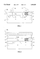
- FIG. 1 shows a cross-section of an in-process integrated circuit structure prior to formation of hypothetically shown copper conductors.
- FIG. 2 shows a first step according to the invention in which a barrier layer (e.g., silicon nitride) that is impermeable to copper or another metal is deposited on the structure of FIG. 1 and a first photoresist layer is thereafter deposited onto the barrier layer.
- a barrier layer e.g., silicon nitride
- FIG. 3 shows a cross-section after a next step in which the first photoresist layer and the barrier layer and are patterned.
- FIG. 4 shows a cross-section after a next step in which the first photoresist layer is stripped off, a metal-phobic layer (e.g. SiO 2 ) is deposited on the patterned barrier layer, and a second photoresist layer is deposited on the metal-phobic layer.
- a metal-phobic layer e.g. SiO 2
- FIG. 5 shows a next cross-section in which the second photoresist layer and the metal-phobic layer are patterned to create windows for implanting a nucleating species into desired surface portions of the barrier layer and/or other portions of the substrate.
- FIG. 6 shows a cross-section after a next step in which a metal (e.g., Cu) which is selectively adhesive to the nucleating species is grown on the surface portions that have the implanted nucleated species.
- a metal e.g., Cu
- FIG. 7 shows a cross-section of an alternate embodiment in which, after the structure of FIG. 5, barrier side walls are formed prior to growth of the metal (e.g., Cu) conductors.
- the metal e.g., Cu
- FIG. 1 shows a cross-section of an in-process integrated circuit structure 100 comprised of a monocrystalline silicon substrate 10, a copper-permeable but Cu-adhesion-phobic first insulating layer 15 (e.g., SiO 2 ) disposed on the silicon substrate, and a metal conductor or via 12 (e.g., Ti or Al) protruding to the top of the first insulating layer 15.
- Metal conductor 12 connects to a first N+ doped portion 10a1 of silicon substrate 10.
- a second N+ doped portion 10a2 of silicon substrate 10 is shown for reasons that will become apparent later.
- a bulk portion 10b of silicon substrate 10 is doped to have a P type conductivity.
- First insulating layer 15 can be thermally grown on silicon substrate 10 or deposited by appropriate means.
- a hypothetical first copper conductor 20a and a hypothetical second copper conductor 20b are shown in cross section as dashed blocks 20a and 20b.
- the hypothetical copper conductors, 20a and 20b, are shown respectively positioned on first insulating layer 15 and metal conductor 12 of FIG. 1 for the purpose of explaining why such a positioning is undesirable.
- FIG. 2 shows a cross section of a second in-process integrated circuit structure 200 formed according to a first step of the invention.
- a barrier layer 17 e.g., a silicon nitride or a silicon oxi-nitride
- CVD chemical vapor deposition
- a first photoresist layer (PR1) 19 is thereafter deposited onto the barrier layer 17.
- the thickness of barrier layer 17 is preferably held equal to 20% or less of the thickness of first insulating layer 15 (e.g., SiO 2 ).
- first insulating layer 15 e.g., SiO 2
- Silicon nitride insulators such as Si 3 N 4 have a relatively high dielectric constant as compared to that of SiO 2 .
- the dielectric constant of SiO 2 is approximately 3.8 while the dielectric constant of Si 3 N 4 is approximately 8.
- An undesirable amount of capacitive coupling may develop between interconnect lines (e.g., between conductor 65 of upcoming FIG. 6 and substrate conductor 10a2) if the barrier layer 17 is made relatively thick and first insulating layer 15 is made relatively thinner.
- layer 17 is made too thick, it becomes difficult to remove a fill material 42 later formed in FIG. 4.
- FIG. 3 shows a cross section of a third in-process integrated circuit structure 300 formed according to a second step of the invention.
- the first photoresist layer (PR1) 19 of structure 200 (FIG. 2) is patterned by appropriate photolithographic means to define an aperture 32 extending through layer 19 over metal conductor 12.
- Barrier layer 17 is thereafter selectively etched to extend aperture 32 through the barrier layer 17 to expose the top surface of metal conductor 12.
- FIG. 4 Shows a cross section of a fourth in-process integrated circuit structure 400 formed according to a third step of the invention.
- the first photoresist layer (PR1) 19 of FIG. 3 is stripped away.
- a second metal-phobic/permeable layer (e.g. SiO 2 or SOG) 40 is deposited by CVD or other appropriate means on the patterned barrier layer 17. Part of the material 42 of the second metal-phobic/permeable layer 40 fills aperture 32.
- the metal-phobic properties of layer 40 are later used in one embodiment of the invention to define the growth profile of a selectively grown conductor (65 and 66 of FIG. 6).
- Layer 40 preferably also has good insulative properties (e.g., high breakdown voltage and low dielectric constant).
- a second photoresist layer (PR2) 44 is thereafter deposited by CVD or other appropriate means on the metal-phobic layer 40.
- FIG. 5 shows a cross section of a fifth in-process integrated circuit structure 500 formed according to a fourth step of the invention.
- the second photoresist layer (PR2) 44 of FIGS. 4 is patterned by appropriate photolithographic means to define apertures 52a and 52b extending through layer 44 as shown.
- Aperture 52b is positioned over metal conductor 12.
- the material of second metal-phobic/permeable layer (SiO 2 ) 40 is selectively etched away to extend aperture 52a to an exposed top surface portion 55 of barrier layer 17 and to extend aperture 52a to an exposed top surface portion 56 of metal conductor 12.
- Apertures 52a and 52b are then used as implant windows for implanting a nucleating species 54, preferably composed of a metal, more preferably composed of a refractory metal and even more preferably selected from the group consisting of molybdenum, tungsten, tantalum and titanium; into the respective top surface portions, 55 and 56, of barrier layer 17 and metal conductor 12.
- the implant energy and material of nucleating species 54 is selected as described further below.
- An ion accelerator can be used to ionize and implant the desired nucleating species 54.
- the second photoresist layer (PR2) 44 of FIG. 5 is stripped away and the implanted top surface portions 55 and 56 are used as respective growth nucleating sites (or growth catalysis sites) for selectively growing copper, or other-metal, conductors 65 and 66.
- Copper can be selectively grown by means of metal-organic chemical vapor deposition (MOCVD) or plasma-enhanced metal-organic chemical vapor deposition (PECVD) or by electroplating.
- MOCVD metal-organic chemical vapor deposition
- PECVD plasma-enhanced metal-organic chemical vapor deposition
- the metal-phobic material of the sidewalls formed by second metal-phobic layer (SiO 2 ) 40 limits the line width of the grown conductors 65 and 66.
- the metal-impermeable material of barrier layer 17 inhibits migration of atoms from the grown copper, or other-metal, conductors 65 and 66 through first insulating layer 15 to the underlying silicon substrate 10.
- the first insulating layer (SiO 2 ) 15 preferably has a lower dielectric constant than the barrier layer (Si 3 N 4 ) 17 so that undesired capacitive coupling between conductor 65 and conductive P or N portions of silicon substrate 10 is minimized.
- Barrier materials such as Si 3 N 4 and oxinitrides tend to have relatively high dielectric constants.
- Insulating materials such as SiO 2 and SOG (Spin On Glass) tend to have lower dielectric constants.
- Low dielectric constant layer 15 is therefore preferably interposed between the substrate 10 and high dielectric layer 17 in cases where capacitive coupling from conductor 65 to conductive region 10a2 of substrate 10 is undesirable.
- the pattern of apertures 52a and 52b formed in FIG. 5 becomes the pattern for the copper or other metal conductors 65 and 66 formed in FIG. 6.
- the two-step, metal coat & remove process is obviated.
- the pattern imprinted into second photoresist layer (PR2) 44 of FIG. 5 becomes the pattern of conductors 65 and 66. Manufacturing cost is reduced and yield is improved by eliminating the problems inherent to the coat & remove process.
- the copper, or other-metal, conductors 65 and 66 can be grown by CVD or more preferably MOCVD (metal organic chemical vapor deposition) techniques or other suitable means.
- the material and concentration of nucleating species 54 are preferably selected to provide a sufficient number of free electrons for exchange with the CVD or MOCVD copper (or other metal) precursor of the CVD or MOCVD process.
- a copper metal-organic precursor such as Cupra SelectTM (a Cu +1 [hexafluoroacetylacetonate)trimethylvinylsilane) which is available from Shumacher Inc. of Carlsbad, Calif. and is described in the above cited paper of J. A. T. Norman et al may be used to grow copper on the implanted top surface portions 55 and 56.
- Cupra SelectTM belongs to a general family of copper metal-organic precursors known as Copper(II) ( ⁇ -diketonate). Other members of the Copper(II) ( ⁇ -diketonate) family may be used. The so-called “hfac” members are preferred. Three preferred members of the "hfac” subfamily are:
- Copper halides such as: (1a) CuCl 2 ; (1b) CuF 2 ; (1c) Cu(hfac) 2 [also known as copper(II) bis(hexafluoro acetylacetonate)]; (1d) Cu(ppm) 2 [also known as copper(II)bis(pentafluoropropanoylpivaloylmethanato)]; (1e) Cu(dpm) 2 [also known as copper(II) bis(dipivaloylmethanato)]; (1f) Cu(nona-F) 2 [also known as copper(II) bis(trifluoroethyl amino hexafluoro pentanol)]; (1g) (CuO-t-Bu) 4 [also known as copper(I) (tert-butoxide)]; (1h) (t-BuO)CuPMe 3 [also known as (tert-butoxy) copper(I) (trimethylphosphine)]
- the candidates for the nucleating species 54 are preferably metals and more preferably, refractory metals selected from the group consisting of molybdenum, tungsten, tantalum and titanium.
- the particular candidate chosen for the nucleating species 54 depends on the desired depth of implant and the amount of damage that is tolerable in the underlying first insulating layer 15 and/or silicon substrate 10 due to overshoot of atoms during implantation and the chemistry of the CVD or MOCVD or other deposition process. More massive atoms such as tungsten have higher kinetic energy and tend to cause more damage to the underlying structures as a result of overshoot during implantation. Medium sized atoms such as molybdenum tend to cause less damage, and hence are preferred.
- the structure 500 of FIG. 5 is modified after removal of second photoresist layer (PR2) 44 by forming barrier (Si 3 N 4 ) sidewalls 75 and 76 in apertures 52a and 52a prior to growth of conductors 65 and 66.
- Barrier sidewalls 75 and 76 are composed of Si 3 N 4 or another metal-impermeable material and they thus provide extra protection against the danger of metal diffusion from conductors 65 and 66 into first insulating layer 15 and/or silicon substrate 10.
- nitrogen-rich silicon oxy-nitrides of the general form SiO x N y may be used as barriers against unwanted diffusion of copper or other metals.
- a neutral species can be ion implanted into the top surface portions 55 and 56 of FIG. 5 for the purpose of providing surface roughening.
- the roughened surface provides a preferential point of nucleation for the later grown or deposited metal conductors 65 and 66.
Abstract
Description
Claims (29)
Priority Applications (2)
| Application Number | Priority Date | Filing Date | Title |
|---|---|---|---|
| US08/036,049 US5654245A (en) | 1993-03-23 | 1993-03-23 | Implantation of nucleating species for selective metallization and products thereof |
| JP02424694A JP3222005B2 (en) | 1993-03-23 | 1994-02-22 | Semiconductor structure and method of manufacturing the same |
Applications Claiming Priority (1)
| Application Number | Priority Date | Filing Date | Title |
|---|---|---|---|
| US08/036,049 US5654245A (en) | 1993-03-23 | 1993-03-23 | Implantation of nucleating species for selective metallization and products thereof |
Publications (1)
| Publication Number | Publication Date |
|---|---|
| US5654245A true US5654245A (en) | 1997-08-05 |
Family
ID=21886319
Family Applications (1)
| Application Number | Title | Priority Date | Filing Date |
|---|---|---|---|
| US08/036,049 Expired - Lifetime US5654245A (en) | 1993-03-23 | 1993-03-23 | Implantation of nucleating species for selective metallization and products thereof |
Country Status (2)
| Country | Link |
|---|---|
| US (1) | US5654245A (en) |
| JP (1) | JP3222005B2 (en) |
Cited By (52)
| Publication number | Priority date | Publication date | Assignee | Title |
|---|---|---|---|---|
| US5891804A (en) * | 1996-04-18 | 1999-04-06 | Texas Instruments Incorporated | Process for conductors with selective deposition |
| US5895261A (en) * | 1995-11-09 | 1999-04-20 | Lsi Logic Corporation | Process for making integrated circuit structure comprising local area interconnects formed over semiconductor substrate by selective deposition on seed layer in patterned trench |
| US5953628A (en) * | 1997-01-28 | 1999-09-14 | Matsushita Electric Industrial Co., Ltd. | Method for forming wiring for a semiconductor device |
| EP0949672A2 (en) * | 1998-04-08 | 1999-10-13 | Texas Instruments Incorporated | PO Flow for copper metallization |
| US5969422A (en) * | 1997-05-15 | 1999-10-19 | Advanced Micro Devices, Inc. | Plated copper interconnect structure |
| US6008117A (en) * | 1996-03-29 | 1999-12-28 | Texas Instruments Incorporated | Method of forming diffusion barriers encapsulating copper |
| US6010962A (en) * | 1999-02-12 | 2000-01-04 | Taiwan Semiconductor Manufacturing Company | Copper chemical-mechanical-polishing (CMP) dishing |
| EP0999584A2 (en) * | 1998-11-06 | 2000-05-10 | Nec Corporation | Method for manufacturing semiconductor device |
| WO2000063966A2 (en) * | 1999-04-01 | 2000-10-26 | Cvc Products, Inc. | Method for planarized deposition of a material |
| US6171661B1 (en) * | 1998-02-25 | 2001-01-09 | Applied Materials, Inc. | Deposition of copper with increased adhesion |
| US6211085B1 (en) | 1999-02-18 | 2001-04-03 | Taiwan Semiconductor Company | Method of preparing CU interconnect lines |
| US6225221B1 (en) * | 2000-02-10 | 2001-05-01 | Chartered Semiconductor Manufacturing Ltd. | Method to deposit a copper seed layer for dual damascene interconnects |
| US6239023B1 (en) | 1999-05-27 | 2001-05-29 | Taiwan Semiconductor Manufacturing Company | Method to reduce the damages of copper lines |
| US6261954B1 (en) * | 2000-02-10 | 2001-07-17 | Chartered Semiconductor Manufacturing, Ltd. | Method to deposit a copper layer |
| WO2001054192A1 (en) * | 2000-01-18 | 2001-07-26 | Micron Technology, Inc. | Process for providing seed layers for aluminium, copper, gold and silver metallurgy |
| US6287968B1 (en) * | 1999-01-04 | 2001-09-11 | Advanced Micro Devices, Inc. | Method of defining copper seed layer for selective electroless plating processing |
| US6294462B1 (en) * | 1997-12-22 | 2001-09-25 | Hyundai Electronics Industries Co., Ltd. | Manufacturing method of interconnection layer for semiconductor device |
| GB2363678A (en) * | 1999-12-22 | 2002-01-02 | Hyundai Electronics Ind | A Method of using a (hfac)Cu(I)(DMB) precursor to form copper wiring |
| US6365972B1 (en) * | 1996-02-28 | 2002-04-02 | Lg Semicon Co., Ltd. | Method for forming a metal wiring structure of a semiconductor device |
| US6420262B1 (en) | 2000-01-18 | 2002-07-16 | Micron Technology, Inc. | Structures and methods to enhance copper metallization |
| US6429120B1 (en) | 2000-01-18 | 2002-08-06 | Micron Technology, Inc. | Methods and apparatus for making integrated-circuit wiring from copper, silver, gold, and other metals |
| US6440852B1 (en) | 1999-01-26 | 2002-08-27 | Agere Systems Guardian Corp. | Integrated circuit including passivated copper interconnection lines and associated manufacturing methods |
| US6495449B1 (en) * | 2000-03-07 | 2002-12-17 | Simplus Systems Corporation | Multilayered diffusion barrier structure for improving adhesion property |
| US6524950B1 (en) * | 2000-02-23 | 2003-02-25 | Taiwan Semiconductor Manufacturing Co., Ltd. | Method of fabricating copper damascene |
| US20030073301A1 (en) * | 2000-03-07 | 2003-04-17 | Tue Nguyen | Multilayered diffusion barrier structure for improving adhesion property |
| US6563222B1 (en) * | 1999-04-19 | 2003-05-13 | Advanced Micro Devices, Inc. | Method and apparatus for reducing electromigration in semiconductor interconnect lines |
| US6579795B1 (en) * | 2002-04-02 | 2003-06-17 | Intel Corporation | Method of making a semiconductor device that has copper damascene interconnects with enhanced electromigration reliability |
| US6614099B2 (en) | 1998-08-04 | 2003-09-02 | Micron Technology, Inc. | Copper metallurgy in integrated circuits |
| US20030186539A1 (en) * | 2002-03-12 | 2003-10-02 | Jong-Myeong Lee | Methods for forming metal interconnections for semiconductor devices having multiple metal depositions |
| US20030194858A1 (en) * | 2000-12-27 | 2003-10-16 | Novellus Systems, Inc. | Method for the formation of diffusion barrier |
| US6661048B2 (en) * | 1999-06-17 | 2003-12-09 | Hitachi, Ltd. | Semiconductor memory device having self-aligned wiring conductor |
| US6683002B1 (en) * | 2000-08-10 | 2004-01-27 | Chartered Semiconductor Manufacturing Ltd. | Method to create a copper diffusion deterrent interface |
| US6703308B1 (en) * | 2001-11-26 | 2004-03-09 | Advanced Micro Devices, Inc. | Method of inserting alloy elements to reduce copper diffusion and bulk diffusion |
| US6703307B2 (en) | 2001-11-26 | 2004-03-09 | Advanced Micro Devices, Inc. | Method of implantation after copper seed deposition |
| US20040219783A1 (en) * | 2001-07-09 | 2004-11-04 | Micron Technology, Inc. | Copper dual damascene interconnect technology |
| US6835655B1 (en) | 2001-11-26 | 2004-12-28 | Advanced Micro Devices, Inc. | Method of implanting copper barrier material to improve electrical performance |
| US6861349B1 (en) | 2002-05-15 | 2005-03-01 | Advanced Micro Devices, Inc. | Method of forming an adhesion layer with an element reactive with a barrier layer |
| US20050059231A1 (en) * | 2000-10-26 | 2005-03-17 | Matsushita Electric Industrial Co., Ltd. | Semiconductor device and method for fabricating the same |
| US20050085073A1 (en) * | 2003-10-16 | 2005-04-21 | Advanced Micro Devices, Inc. | Method of using an adhesion precursor layer for chemical vapor deposition (CVD) copper deposition |
| US6995470B2 (en) | 2000-05-31 | 2006-02-07 | Micron Technology, Inc. | Multilevel copper interconnects with low-k dielectrics and air gaps |
| US20060040491A1 (en) * | 2004-08-21 | 2006-02-23 | Lim Yeow K | Slot designs in wide metal lines |
| US7067421B2 (en) | 2000-05-31 | 2006-06-27 | Micron Technology, Inc. | Multilevel copper interconnect with double passivation |
| WO2006102182A2 (en) * | 2005-03-18 | 2006-09-28 | Applied Materials, Inc. | Process for electroless copper deposition |
| US7211512B1 (en) | 2000-01-18 | 2007-05-01 | Micron Technology, Inc. | Selective electroless-plated copper metallization |
| US7220665B2 (en) | 2003-08-05 | 2007-05-22 | Micron Technology, Inc. | H2 plasma treatment |
| US7223694B2 (en) * | 2003-06-10 | 2007-05-29 | Intel Corporation | Method for improving selectivity of electroless metal deposition |
| US7253521B2 (en) | 2000-01-18 | 2007-08-07 | Micron Technology, Inc. | Methods for making integrated-circuit wiring from copper, silver, gold, and other metals |
| US7651934B2 (en) | 2005-03-18 | 2010-01-26 | Applied Materials, Inc. | Process for electroless copper deposition |
| US7696092B2 (en) | 2001-11-26 | 2010-04-13 | Globalfoundries Inc. | Method of using ternary copper alloy to obtain a low resistance and large grain size interconnect |
| US9754791B2 (en) * | 2015-02-07 | 2017-09-05 | Applied Materials, Inc. | Selective deposition utilizing masks and directional plasma treatment |
| US10103057B2 (en) | 2014-11-11 | 2018-10-16 | The Board Of Trustees Of The University Of Illinois | Use of an inhibitor molecule in chemical vapor deposition to afford deposition of copper on a metal substrate with no deposition on adjacent SIO2 substrate |
| US11584986B1 (en) | 2017-11-01 | 2023-02-21 | The Board Of Trustees Of The University Of Illinois | Area selective CVD of metallic films using precursor gases and inhibitors |
Citations (7)
| Publication number | Priority date | Publication date | Assignee | Title |
|---|---|---|---|---|
| US4746621A (en) * | 1986-12-05 | 1988-05-24 | Cornell Research Foundation, Inc. | Planar tungsten interconnect |
| US4907066A (en) * | 1986-12-05 | 1990-03-06 | Cornell Research Foundation, Inc. | Planar tungsten interconnect with implanted silicon |
| JPH02162722A (en) * | 1988-12-16 | 1990-06-22 | Nippon Telegr & Teleph Corp <Ntt> | Manufacture of semiconductor device |
| US5154949A (en) * | 1989-09-26 | 1992-10-13 | Canon Kabushiki Kaisha | Process for forming metal deposited film containing aluminum as main component by use of alkyl aluminum hydride |
| US5180687A (en) * | 1989-09-26 | 1993-01-19 | Canon Kabushiki Kaisha | Deposited film formation method utilizing selective deposition by use of alkyl aluminum hydride |
| US5183795A (en) * | 1989-12-13 | 1993-02-02 | Intel Corporation | Fully planar metalization process |
| US5459100A (en) * | 1993-12-21 | 1995-10-17 | Hyundai Electronics Industries Co., Ltd. | Method for forming metal wiring of semiconductor device |
-
1993
- 1993-03-23 US US08/036,049 patent/US5654245A/en not_active Expired - Lifetime
-
1994
- 1994-02-22 JP JP02424694A patent/JP3222005B2/en not_active Expired - Fee Related
Patent Citations (7)
| Publication number | Priority date | Publication date | Assignee | Title |
|---|---|---|---|---|
| US4746621A (en) * | 1986-12-05 | 1988-05-24 | Cornell Research Foundation, Inc. | Planar tungsten interconnect |
| US4907066A (en) * | 1986-12-05 | 1990-03-06 | Cornell Research Foundation, Inc. | Planar tungsten interconnect with implanted silicon |
| JPH02162722A (en) * | 1988-12-16 | 1990-06-22 | Nippon Telegr & Teleph Corp <Ntt> | Manufacture of semiconductor device |
| US5154949A (en) * | 1989-09-26 | 1992-10-13 | Canon Kabushiki Kaisha | Process for forming metal deposited film containing aluminum as main component by use of alkyl aluminum hydride |
| US5180687A (en) * | 1989-09-26 | 1993-01-19 | Canon Kabushiki Kaisha | Deposited film formation method utilizing selective deposition by use of alkyl aluminum hydride |
| US5183795A (en) * | 1989-12-13 | 1993-02-02 | Intel Corporation | Fully planar metalization process |
| US5459100A (en) * | 1993-12-21 | 1995-10-17 | Hyundai Electronics Industries Co., Ltd. | Method for forming metal wiring of semiconductor device |
Non-Patent Citations (14)
| Title |
|---|
| B. Rogers et al., "Issues in a Submicron Cu Interconnect System Using Liftoff Patterning", IEEE VMIC Conference Proceedings, Jun. 1991, pp. 137-143. |
| B. Rogers et al., Issues in a Submicron Cu Interconnect System Using Liftoff Patterning , IEEE VMIC Conference Proceedings, Jun. 1991, pp. 137 143. * |
| D.C. Thomas et al., "A Multilevel Tungsten Interconnect Technology", Tech Digest, IEDM 1988, pp. 466-469. |
| D.C. Thomas et al., A Multilevel Tungsten Interconnect Technology , Tech Digest, IEDM 1988, pp. 466 469. * |
| D.S. Gardner et al., "Encapsulated Copper Interconnection Devices Using Sidewall Barriers", VMIC Conference Proceedings, Jun. 1991, pp. 99-108. |
| D.S. Gardner et al., Encapsulated Copper Interconnection Devices Using Sidewall Barriers , VMIC Conference Proceedings, Jun. 1991, pp. 99 108. * |
| J.A.T. Normal et al., "New OMCVD Precursors For Selective Copper Metallization", VMIC Conference Proceedings, Jun. 1991, pp. 123-129. |
| J.A.T. Normal et al., New OMCVD Precursors For Selective Copper Metallization , VMIC Conference Proceedings, Jun. 1991, pp. 123 129. * |
| J.D. McBrayer et al., "Diffusion of Metals in Silicon Dioxide", J. Electrochem. Soc., vol. 133, Jun. 1986, pp. 1242-1246. |
| J.D. McBrayer et al., Diffusion of Metals in Silicon Dioxide , J. Electrochem. Soc., vol. 133, Jun. 1986, pp. 1242 1246. * |
| J.S.H. Cho et al., "Copper Interconnection with Tungsten Cladding for ULSI", 1991 Symposium on VLSI Technology, Oiso, Japan, pp. 37-40. |
| J.S.H. Cho et al., Copper Interconnection with Tungsten Cladding for ULSI , 1991 Symposium on VLSI Technology, Oiso, Japan, pp. 37 40. * |
| S. Wolf et al., "Silicon Processing for the VLSI Era", Process Technology, vol. 1 & 2 Lattice Press (1986), pp. 261, 403. |
| S. Wolf et al., Silicon Processing for the VLSI Era , Process Technology, vol. 1 & 2 Lattice Press (1986), pp. 261, 403. * |
Cited By (88)
| Publication number | Priority date | Publication date | Assignee | Title |
|---|---|---|---|---|
| US5895261A (en) * | 1995-11-09 | 1999-04-20 | Lsi Logic Corporation | Process for making integrated circuit structure comprising local area interconnects formed over semiconductor substrate by selective deposition on seed layer in patterned trench |
| US6365972B1 (en) * | 1996-02-28 | 2002-04-02 | Lg Semicon Co., Ltd. | Method for forming a metal wiring structure of a semiconductor device |
| US6008117A (en) * | 1996-03-29 | 1999-12-28 | Texas Instruments Incorporated | Method of forming diffusion barriers encapsulating copper |
| US5891804A (en) * | 1996-04-18 | 1999-04-06 | Texas Instruments Incorporated | Process for conductors with selective deposition |
| US5953628A (en) * | 1997-01-28 | 1999-09-14 | Matsushita Electric Industrial Co., Ltd. | Method for forming wiring for a semiconductor device |
| US5969422A (en) * | 1997-05-15 | 1999-10-19 | Advanced Micro Devices, Inc. | Plated copper interconnect structure |
| US6294462B1 (en) * | 1997-12-22 | 2001-09-25 | Hyundai Electronics Industries Co., Ltd. | Manufacturing method of interconnection layer for semiconductor device |
| US6171661B1 (en) * | 1998-02-25 | 2001-01-09 | Applied Materials, Inc. | Deposition of copper with increased adhesion |
| US6355106B1 (en) * | 1998-02-25 | 2002-03-12 | Applied Materials, Inc. | Deposition of copper with increased adhesion |
| EP0949672A2 (en) * | 1998-04-08 | 1999-10-13 | Texas Instruments Incorporated | PO Flow for copper metallization |
| EP0949672A3 (en) * | 1998-04-08 | 2002-09-11 | Texas Instruments Incorporated | PO Flow for copper metallization |
| US6614099B2 (en) | 1998-08-04 | 2003-09-02 | Micron Technology, Inc. | Copper metallurgy in integrated circuits |
| EP0999584A2 (en) * | 1998-11-06 | 2000-05-10 | Nec Corporation | Method for manufacturing semiconductor device |
| EP0999584A3 (en) * | 1998-11-06 | 2000-08-30 | Nec Corporation | Method for manufacturing semiconductor device |
| US6136708A (en) * | 1998-11-06 | 2000-10-24 | Nec Corporation | Method for manufacturing semiconductor device |
| US6287968B1 (en) * | 1999-01-04 | 2001-09-11 | Advanced Micro Devices, Inc. | Method of defining copper seed layer for selective electroless plating processing |
| US6440852B1 (en) | 1999-01-26 | 2002-08-27 | Agere Systems Guardian Corp. | Integrated circuit including passivated copper interconnection lines and associated manufacturing methods |
| US6010962A (en) * | 1999-02-12 | 2000-01-04 | Taiwan Semiconductor Manufacturing Company | Copper chemical-mechanical-polishing (CMP) dishing |
| US6211085B1 (en) | 1999-02-18 | 2001-04-03 | Taiwan Semiconductor Company | Method of preparing CU interconnect lines |
| US6245655B1 (en) | 1999-04-01 | 2001-06-12 | Cvc Products, Inc. | Method for planarized deposition of a material |
| WO2000063966A2 (en) * | 1999-04-01 | 2000-10-26 | Cvc Products, Inc. | Method for planarized deposition of a material |
| WO2000063966A3 (en) * | 1999-04-01 | 2001-04-05 | Cvc Products Inc | Method for planarized deposition of a material |
| US6563222B1 (en) * | 1999-04-19 | 2003-05-13 | Advanced Micro Devices, Inc. | Method and apparatus for reducing electromigration in semiconductor interconnect lines |
| US6239023B1 (en) | 1999-05-27 | 2001-05-29 | Taiwan Semiconductor Manufacturing Company | Method to reduce the damages of copper lines |
| US6500753B2 (en) | 1999-05-27 | 2002-12-31 | Taiwan Semiconductor Manufacturing Company | Method to reduce the damages of copper lines |
| US6661048B2 (en) * | 1999-06-17 | 2003-12-09 | Hitachi, Ltd. | Semiconductor memory device having self-aligned wiring conductor |
| GB2363678B (en) * | 1999-12-22 | 2004-07-07 | Hyundai Electronics Ind | Method of forming a copper wiring in a semiconductor device |
| GB2363678A (en) * | 1999-12-22 | 2002-01-02 | Hyundai Electronics Ind | A Method of using a (hfac)Cu(I)(DMB) precursor to form copper wiring |
| US7535103B2 (en) | 2000-01-18 | 2009-05-19 | Micron Technology, Inc. | Structures and methods to enhance copper metallization |
| US7105914B2 (en) | 2000-01-18 | 2006-09-12 | Micron Technology, Inc. | Integrated circuit and seed layers |
| US7211512B1 (en) | 2000-01-18 | 2007-05-01 | Micron Technology, Inc. | Selective electroless-plated copper metallization |
| US6420262B1 (en) | 2000-01-18 | 2002-07-16 | Micron Technology, Inc. | Structures and methods to enhance copper metallization |
| US7262130B1 (en) | 2000-01-18 | 2007-08-28 | Micron Technology, Inc. | Methods for making integrated-circuit wiring from copper, silver, gold, and other metals |
| US7262505B2 (en) * | 2000-01-18 | 2007-08-28 | Micron Technology, Inc. | Selective electroless-plated copper metallization |
| US7285196B2 (en) | 2000-01-18 | 2007-10-23 | Micron Technology, Inc. | Methods and apparatus for making integrated-circuit wiring from copper, silver, gold, and other metals |
| US6376370B1 (en) | 2000-01-18 | 2002-04-23 | Micron Technology, Inc. | Process for providing seed layers for using aluminum, copper, gold and silver metallurgy process for providing seed layers for using aluminum, copper, gold and silver metallurgy |
| US8779596B2 (en) | 2000-01-18 | 2014-07-15 | Micron Technology, Inc. | Structures and methods to enhance copper metallization |
| US7253521B2 (en) | 2000-01-18 | 2007-08-07 | Micron Technology, Inc. | Methods for making integrated-circuit wiring from copper, silver, gold, and other metals |
| US7745934B2 (en) | 2000-01-18 | 2010-06-29 | Micron Technology, Inc. | Integrated circuit and seed layers |
| US7301190B2 (en) | 2000-01-18 | 2007-11-27 | Micron Technology, Inc. | Structures and methods to enhance copper metallization |
| WO2001054192A1 (en) * | 2000-01-18 | 2001-07-26 | Micron Technology, Inc. | Process for providing seed layers for aluminium, copper, gold and silver metallurgy |
| US7368378B2 (en) | 2000-01-18 | 2008-05-06 | Micron Technology, Inc. | Methods for making integrated-circuit wiring from copper, silver, gold, and other metals |
| US7378737B2 (en) | 2000-01-18 | 2008-05-27 | Micron Technology, Inc. | Structures and methods to enhance copper metallization |
| US7394157B2 (en) | 2000-01-18 | 2008-07-01 | Micron Technology, Inc. | Integrated circuit and seed layers |
| US7670469B2 (en) | 2000-01-18 | 2010-03-02 | Micron Technology, Inc. | Methods and apparatus for making integrated-circuit wiring from copper, silver, gold, and other metals |
| US6743716B2 (en) | 2000-01-18 | 2004-06-01 | Micron Technology, Inc. | Structures and methods to enhance copper metallization |
| US6756298B2 (en) | 2000-01-18 | 2004-06-29 | Micron Technology, Inc. | Methods and apparatus for making integrated-circuit wiring from copper, silver, gold, and other metals |
| US6429120B1 (en) | 2000-01-18 | 2002-08-06 | Micron Technology, Inc. | Methods and apparatus for making integrated-circuit wiring from copper, silver, gold, and other metals |
| US6225221B1 (en) * | 2000-02-10 | 2001-05-01 | Chartered Semiconductor Manufacturing Ltd. | Method to deposit a copper seed layer for dual damascene interconnects |
| US6261954B1 (en) * | 2000-02-10 | 2001-07-17 | Chartered Semiconductor Manufacturing, Ltd. | Method to deposit a copper layer |
| SG87157A1 (en) * | 2000-02-10 | 2002-03-19 | Chartered Semiconductor Mfg | Method to deposit a copper layer |
| SG93880A1 (en) * | 2000-02-10 | 2003-01-21 | Chartered Semiconductor Mfg | Method to deposit a copper seed layer for dual damascene interconnects |
| US6524950B1 (en) * | 2000-02-23 | 2003-02-25 | Taiwan Semiconductor Manufacturing Co., Ltd. | Method of fabricating copper damascene |
| US20030073301A1 (en) * | 2000-03-07 | 2003-04-17 | Tue Nguyen | Multilayered diffusion barrier structure for improving adhesion property |
| US6495449B1 (en) * | 2000-03-07 | 2002-12-17 | Simplus Systems Corporation | Multilayered diffusion barrier structure for improving adhesion property |
| US6670266B2 (en) * | 2000-03-07 | 2003-12-30 | Simplus Systems Corporation | Multilayered diffusion barrier structure for improving adhesion property |
| US7091611B2 (en) | 2000-05-31 | 2006-08-15 | Micron Technology, Inc. | Multilevel copper interconnects with low-k dielectrics and air gaps |
| US6995470B2 (en) | 2000-05-31 | 2006-02-07 | Micron Technology, Inc. | Multilevel copper interconnects with low-k dielectrics and air gaps |
| US7067421B2 (en) | 2000-05-31 | 2006-06-27 | Micron Technology, Inc. | Multilevel copper interconnect with double passivation |
| US6683002B1 (en) * | 2000-08-10 | 2004-01-27 | Chartered Semiconductor Manufacturing Ltd. | Method to create a copper diffusion deterrent interface |
| SG116423A1 (en) * | 2000-08-10 | 2005-11-28 | Chartered Semiconductor Mfg | A method to create a copper diffusion deterrent interface. |
| US20050059231A1 (en) * | 2000-10-26 | 2005-03-17 | Matsushita Electric Industrial Co., Ltd. | Semiconductor device and method for fabricating the same |
| US7144761B2 (en) * | 2000-10-26 | 2006-12-05 | Matsushita Electric Industrial Co., Ltd. | Semiconductor device and method for fabricating the same |
| US6887781B2 (en) * | 2000-12-27 | 2005-05-03 | Novellus Systems, Inc. | Method for the formation of diffusion barrier |
| US20030194858A1 (en) * | 2000-12-27 | 2003-10-16 | Novellus Systems, Inc. | Method for the formation of diffusion barrier |
| US20040219783A1 (en) * | 2001-07-09 | 2004-11-04 | Micron Technology, Inc. | Copper dual damascene interconnect technology |
| US6703308B1 (en) * | 2001-11-26 | 2004-03-09 | Advanced Micro Devices, Inc. | Method of inserting alloy elements to reduce copper diffusion and bulk diffusion |
| US7696092B2 (en) | 2001-11-26 | 2010-04-13 | Globalfoundries Inc. | Method of using ternary copper alloy to obtain a low resistance and large grain size interconnect |
| US6703307B2 (en) | 2001-11-26 | 2004-03-09 | Advanced Micro Devices, Inc. | Method of implantation after copper seed deposition |
| US6835655B1 (en) | 2001-11-26 | 2004-12-28 | Advanced Micro Devices, Inc. | Method of implanting copper barrier material to improve electrical performance |
| US6964922B2 (en) * | 2002-03-12 | 2005-11-15 | Samsung Electronics Co., Ltd. | Methods for forming metal interconnections for semiconductor devices having multiple metal depositions |
| US20030186539A1 (en) * | 2002-03-12 | 2003-10-02 | Jong-Myeong Lee | Methods for forming metal interconnections for semiconductor devices having multiple metal depositions |
| US6579795B1 (en) * | 2002-04-02 | 2003-06-17 | Intel Corporation | Method of making a semiconductor device that has copper damascene interconnects with enhanced electromigration reliability |
| US6861349B1 (en) | 2002-05-15 | 2005-03-01 | Advanced Micro Devices, Inc. | Method of forming an adhesion layer with an element reactive with a barrier layer |
| US7223694B2 (en) * | 2003-06-10 | 2007-05-29 | Intel Corporation | Method for improving selectivity of electroless metal deposition |
| US7504674B2 (en) | 2003-08-05 | 2009-03-17 | Micron Technology, Inc. | Electronic apparatus having a core conductive structure within an insulating layer |
| US7220665B2 (en) | 2003-08-05 | 2007-05-22 | Micron Technology, Inc. | H2 plasma treatment |
| US7169706B2 (en) | 2003-10-16 | 2007-01-30 | Advanced Micro Devices, Inc. | Method of using an adhesion precursor layer for chemical vapor deposition (CVD) copper deposition |
| US20050085073A1 (en) * | 2003-10-16 | 2005-04-21 | Advanced Micro Devices, Inc. | Method of using an adhesion precursor layer for chemical vapor deposition (CVD) copper deposition |
| US20060040491A1 (en) * | 2004-08-21 | 2006-02-23 | Lim Yeow K | Slot designs in wide metal lines |
| US9318378B2 (en) * | 2004-08-21 | 2016-04-19 | Globalfoundries Singapore Pte. Ltd. | Slot designs in wide metal lines |
| WO2006102182A2 (en) * | 2005-03-18 | 2006-09-28 | Applied Materials, Inc. | Process for electroless copper deposition |
| US7651934B2 (en) | 2005-03-18 | 2010-01-26 | Applied Materials, Inc. | Process for electroless copper deposition |
| WO2006102182A3 (en) * | 2005-03-18 | 2007-03-01 | Applied Materials Inc | Process for electroless copper deposition |
| US10103057B2 (en) | 2014-11-11 | 2018-10-16 | The Board Of Trustees Of The University Of Illinois | Use of an inhibitor molecule in chemical vapor deposition to afford deposition of copper on a metal substrate with no deposition on adjacent SIO2 substrate |
| US9754791B2 (en) * | 2015-02-07 | 2017-09-05 | Applied Materials, Inc. | Selective deposition utilizing masks and directional plasma treatment |
| TWI675397B (en) * | 2015-02-07 | 2019-10-21 | 美商應用材料股份有限公司 | Selective deposition utilizing masks and directional plasma treatment |
| US11584986B1 (en) | 2017-11-01 | 2023-02-21 | The Board Of Trustees Of The University Of Illinois | Area selective CVD of metallic films using precursor gases and inhibitors |
Also Published As
| Publication number | Publication date |
|---|---|
| JP3222005B2 (en) | 2001-10-22 |
| JPH077078A (en) | 1995-01-10 |
Similar Documents
| Publication | Publication Date | Title |
|---|---|---|
| US5654245A (en) | Implantation of nucleating species for selective metallization and products thereof | |
| KR100268213B1 (en) | An open-bottomed via liner structure and method for fabricating same | |
| US5930669A (en) | Continuous highly conductive metal wiring structures and method for fabricating the same | |
| US6458684B1 (en) | Single step process for blanket-selective CVD aluminum deposition | |
| EP0892428B1 (en) | Method of producing low resistance contacts between integrated circuit metal levels and structure produced thereby. | |
| US6933230B2 (en) | Method for making interconnects and diffusion barriers in integrated circuits | |
| US6537905B1 (en) | Fully planarized dual damascene metallization using copper line interconnect and selective CVD aluminum plug | |
| US5227335A (en) | Tungsten metallization | |
| EP0370775B1 (en) | Method of manufacturing semiconductor device | |
| US7186638B2 (en) | Passivation processes for use with metallization techniques | |
| US5960320A (en) | Metal wiring layer forming method for semiconductor device | |
| GB2234394A (en) | Forming metal interconnexions | |
| EP0504984B1 (en) | Method of making a connection on a semiconductor device | |
| US5851367A (en) | Differential copper deposition on integrated circuit surfaces and method for same | |
| KR20010033664A (en) | A single step electroplating process for interconnect via fill and metal line patterning | |
| EP0267730B1 (en) | Tungsten metallization | |
| GB2295724A (en) | Semiconductor device and method of making a plug | |
| KR940011732B1 (en) | Manufacturing method of semiconductor device | |
| EP0805489A2 (en) | Selective via fill using a sacrificial layer | |
| CN1074857C (en) | Method for forming metal wiring of semiconductor device | |
| JP4937437B2 (en) | Method for improving the properties of metal layers deposited from plating baths | |
| EP0256917A1 (en) | Method of producing interconnection layers using CVD of metal | |
| US20230223447A1 (en) | Buried near-gate local interconnects and methods of their manufacture | |
| EP0543254B1 (en) | A method of forming high-stability metallic contacts in an integrated circuit with one or more metallized layers | |
| KR100236095B1 (en) | Interconnecting method of semiconductor device |
Legal Events
| Date | Code | Title | Description |
|---|---|---|---|
| STPP | Information on status: patent application and granting procedure in general |
Free format text: APPLICATION UNDERGOING PREEXAM PROCESSING |
|
| AS | Assignment |
Owner name: SHARP MICROELECTRONICS TECHNOLOGY, INC., WASHINGTO Free format text: ASSIGNMENT OF ASSIGNORS INTEREST;ASSIGNOR:ALLEN, GREGORY LEE;REEL/FRAME:006556/0611 Effective date: 19930510 |
|
| AS | Assignment |
Owner name: SHARP KABUSHIKI KAISHA, JAPAN Free format text: ASSIGNMENT OF ASSIGNORS INTEREST;ASSIGNOR:SHARP MICROELECTRONICS TECHNOLOGY, INC.;REEL/FRAME:007200/0842 Effective date: 19941019 |
|
| AS | Assignment |
Owner name: SHARP LABORATORIES OF AMERICA, INC., WASHINGTON Free format text: ASSIGNMENT OF ASSIGNORS INTEREST;ASSIGNOR:SHARP MICROELECTRONICS TECHNOLOGY, INC.;REEL/FRAME:009845/0188 Effective date: 19990330 |
|
| FEPP | Fee payment procedure |
Free format text: PAYOR NUMBER ASSIGNED (ORIGINAL EVENT CODE: ASPN); ENTITY STATUS OF PATENT OWNER: LARGE ENTITY |
|
| FPAY | Fee payment |
Year of fee payment: 4 |
|
| FPAY | Fee payment |
Year of fee payment: 8 |
|
| FPAY | Fee payment |
Year of fee payment: 12 |