US5672909A - Interdigitated wirebond programmable fixed voltage planes - Google Patents
Interdigitated wirebond programmable fixed voltage planes Download PDFInfo
- Publication number
- US5672909A US5672909A US08/688,083 US68808396A US5672909A US 5672909 A US5672909 A US 5672909A US 68808396 A US68808396 A US 68808396A US 5672909 A US5672909 A US 5672909A
- Authority
- US
- United States
- Prior art keywords
- bus
- buses
- die
- level
- fingers
- Prior art date
- Legal status (The legal status is an assumption and is not a legal conclusion. Google has not performed a legal analysis and makes no representation as to the accuracy of the status listed.)
- Expired - Lifetime
Links
Images


Classifications
-
- H—ELECTRICITY
- H01—ELECTRIC ELEMENTS
- H01L—SEMICONDUCTOR DEVICES NOT COVERED BY CLASS H10
- H01L23/00—Details of semiconductor or other solid state devices
- H01L23/48—Arrangements for conducting electric current to or from the solid state body in operation, e.g. leads, terminal arrangements ; Selection of materials therefor
- H01L23/50—Arrangements for conducting electric current to or from the solid state body in operation, e.g. leads, terminal arrangements ; Selection of materials therefor for integrated circuit devices, e.g. power bus, number of leads
-
- H—ELECTRICITY
- H01—ELECTRIC ELEMENTS
- H01L—SEMICONDUCTOR DEVICES NOT COVERED BY CLASS H10
- H01L24/00—Arrangements for connecting or disconnecting semiconductor or solid-state bodies; Methods or apparatus related thereto
- H01L24/01—Means for bonding being attached to, or being formed on, the surface to be connected, e.g. chip-to-package, die-attach, "first-level" interconnects; Manufacturing methods related thereto
- H01L24/42—Wire connectors; Manufacturing methods related thereto
- H01L24/47—Structure, shape, material or disposition of the wire connectors after the connecting process
- H01L24/49—Structure, shape, material or disposition of the wire connectors after the connecting process of a plurality of wire connectors
-
- H—ELECTRICITY
- H01—ELECTRIC ELEMENTS
- H01L—SEMICONDUCTOR DEVICES NOT COVERED BY CLASS H10
- H01L2224/00—Indexing scheme for arrangements for connecting or disconnecting semiconductor or solid-state bodies and methods related thereto as covered by H01L24/00
- H01L2224/01—Means for bonding being attached to, or being formed on, the surface to be connected, e.g. chip-to-package, die-attach, "first-level" interconnects; Manufacturing methods related thereto
- H01L2224/02—Bonding areas; Manufacturing methods related thereto
- H01L2224/04—Structure, shape, material or disposition of the bonding areas prior to the connecting process
- H01L2224/05—Structure, shape, material or disposition of the bonding areas prior to the connecting process of an individual bonding area
- H01L2224/0554—External layer
- H01L2224/0555—Shape
- H01L2224/05552—Shape in top view
- H01L2224/05554—Shape in top view being square
-
- H—ELECTRICITY
- H01—ELECTRIC ELEMENTS
- H01L—SEMICONDUCTOR DEVICES NOT COVERED BY CLASS H10
- H01L2224/00—Indexing scheme for arrangements for connecting or disconnecting semiconductor or solid-state bodies and methods related thereto as covered by H01L24/00
- H01L2224/01—Means for bonding being attached to, or being formed on, the surface to be connected, e.g. chip-to-package, die-attach, "first-level" interconnects; Manufacturing methods related thereto
- H01L2224/42—Wire connectors; Manufacturing methods related thereto
- H01L2224/47—Structure, shape, material or disposition of the wire connectors after the connecting process
- H01L2224/48—Structure, shape, material or disposition of the wire connectors after the connecting process of an individual wire connector
- H01L2224/4801—Structure
- H01L2224/48011—Length
-
- H—ELECTRICITY
- H01—ELECTRIC ELEMENTS
- H01L—SEMICONDUCTOR DEVICES NOT COVERED BY CLASS H10
- H01L2224/00—Indexing scheme for arrangements for connecting or disconnecting semiconductor or solid-state bodies and methods related thereto as covered by H01L24/00
- H01L2224/01—Means for bonding being attached to, or being formed on, the surface to be connected, e.g. chip-to-package, die-attach, "first-level" interconnects; Manufacturing methods related thereto
- H01L2224/42—Wire connectors; Manufacturing methods related thereto
- H01L2224/47—Structure, shape, material or disposition of the wire connectors after the connecting process
- H01L2224/48—Structure, shape, material or disposition of the wire connectors after the connecting process of an individual wire connector
- H01L2224/4805—Shape
- H01L2224/4809—Loop shape
- H01L2224/48091—Arched
-
- H—ELECTRICITY
- H01—ELECTRIC ELEMENTS
- H01L—SEMICONDUCTOR DEVICES NOT COVERED BY CLASS H10
- H01L2224/00—Indexing scheme for arrangements for connecting or disconnecting semiconductor or solid-state bodies and methods related thereto as covered by H01L24/00
- H01L2224/01—Means for bonding being attached to, or being formed on, the surface to be connected, e.g. chip-to-package, die-attach, "first-level" interconnects; Manufacturing methods related thereto
- H01L2224/42—Wire connectors; Manufacturing methods related thereto
- H01L2224/47—Structure, shape, material or disposition of the wire connectors after the connecting process
- H01L2224/48—Structure, shape, material or disposition of the wire connectors after the connecting process of an individual wire connector
- H01L2224/481—Disposition
- H01L2224/48151—Connecting between a semiconductor or solid-state body and an item not being a semiconductor or solid-state body, e.g. chip-to-substrate, chip-to-passive
- H01L2224/48221—Connecting between a semiconductor or solid-state body and an item not being a semiconductor or solid-state body, e.g. chip-to-substrate, chip-to-passive the body and the item being stacked
- H01L2224/48225—Connecting between a semiconductor or solid-state body and an item not being a semiconductor or solid-state body, e.g. chip-to-substrate, chip-to-passive the body and the item being stacked the item being non-metallic, e.g. insulating substrate with or without metallisation
- H01L2224/48227—Connecting between a semiconductor or solid-state body and an item not being a semiconductor or solid-state body, e.g. chip-to-substrate, chip-to-passive the body and the item being stacked the item being non-metallic, e.g. insulating substrate with or without metallisation connecting the wire to a bond pad of the item
-
- H—ELECTRICITY
- H01—ELECTRIC ELEMENTS
- H01L—SEMICONDUCTOR DEVICES NOT COVERED BY CLASS H10
- H01L2224/00—Indexing scheme for arrangements for connecting or disconnecting semiconductor or solid-state bodies and methods related thereto as covered by H01L24/00
- H01L2224/01—Means for bonding being attached to, or being formed on, the surface to be connected, e.g. chip-to-package, die-attach, "first-level" interconnects; Manufacturing methods related thereto
- H01L2224/42—Wire connectors; Manufacturing methods related thereto
- H01L2224/47—Structure, shape, material or disposition of the wire connectors after the connecting process
- H01L2224/48—Structure, shape, material or disposition of the wire connectors after the connecting process of an individual wire connector
- H01L2224/484—Connecting portions
- H01L2224/4847—Connecting portions the connecting portion on the bonding area of the semiconductor or solid-state body being a wedge bond
- H01L2224/48472—Connecting portions the connecting portion on the bonding area of the semiconductor or solid-state body being a wedge bond the other connecting portion not on the bonding area also being a wedge bond, i.e. wedge-to-wedge
-
- H—ELECTRICITY
- H01—ELECTRIC ELEMENTS
- H01L—SEMICONDUCTOR DEVICES NOT COVERED BY CLASS H10
- H01L2224/00—Indexing scheme for arrangements for connecting or disconnecting semiconductor or solid-state bodies and methods related thereto as covered by H01L24/00
- H01L2224/01—Means for bonding being attached to, or being formed on, the surface to be connected, e.g. chip-to-package, die-attach, "first-level" interconnects; Manufacturing methods related thereto
- H01L2224/42—Wire connectors; Manufacturing methods related thereto
- H01L2224/47—Structure, shape, material or disposition of the wire connectors after the connecting process
- H01L2224/49—Structure, shape, material or disposition of the wire connectors after the connecting process of a plurality of wire connectors
- H01L2224/491—Disposition
- H01L2224/49105—Connecting at different heights
- H01L2224/49109—Connecting at different heights outside the semiconductor or solid-state body
-
- H—ELECTRICITY
- H01—ELECTRIC ELEMENTS
- H01L—SEMICONDUCTOR DEVICES NOT COVERED BY CLASS H10
- H01L2224/00—Indexing scheme for arrangements for connecting or disconnecting semiconductor or solid-state bodies and methods related thereto as covered by H01L24/00
- H01L2224/01—Means for bonding being attached to, or being formed on, the surface to be connected, e.g. chip-to-package, die-attach, "first-level" interconnects; Manufacturing methods related thereto
- H01L2224/42—Wire connectors; Manufacturing methods related thereto
- H01L2224/47—Structure, shape, material or disposition of the wire connectors after the connecting process
- H01L2224/49—Structure, shape, material or disposition of the wire connectors after the connecting process of a plurality of wire connectors
- H01L2224/491—Disposition
- H01L2224/4911—Disposition the connectors being bonded to at least one common bonding area, e.g. daisy chain
-
- H—ELECTRICITY
- H01—ELECTRIC ELEMENTS
- H01L—SEMICONDUCTOR DEVICES NOT COVERED BY CLASS H10
- H01L2224/00—Indexing scheme for arrangements for connecting or disconnecting semiconductor or solid-state bodies and methods related thereto as covered by H01L24/00
- H01L2224/01—Means for bonding being attached to, or being formed on, the surface to be connected, e.g. chip-to-package, die-attach, "first-level" interconnects; Manufacturing methods related thereto
- H01L2224/42—Wire connectors; Manufacturing methods related thereto
- H01L2224/47—Structure, shape, material or disposition of the wire connectors after the connecting process
- H01L2224/49—Structure, shape, material or disposition of the wire connectors after the connecting process of a plurality of wire connectors
- H01L2224/491—Disposition
- H01L2224/4912—Layout
- H01L2224/49175—Parallel arrangements
-
- H—ELECTRICITY
- H01—ELECTRIC ELEMENTS
- H01L—SEMICONDUCTOR DEVICES NOT COVERED BY CLASS H10
- H01L2224/00—Indexing scheme for arrangements for connecting or disconnecting semiconductor or solid-state bodies and methods related thereto as covered by H01L24/00
- H01L2224/01—Means for bonding being attached to, or being formed on, the surface to be connected, e.g. chip-to-package, die-attach, "first-level" interconnects; Manufacturing methods related thereto
- H01L2224/42—Wire connectors; Manufacturing methods related thereto
- H01L2224/47—Structure, shape, material or disposition of the wire connectors after the connecting process
- H01L2224/49—Structure, shape, material or disposition of the wire connectors after the connecting process of a plurality of wire connectors
- H01L2224/494—Connecting portions
- H01L2224/4943—Connecting portions the connecting portions being staggered
-
- H—ELECTRICITY
- H01—ELECTRIC ELEMENTS
- H01L—SEMICONDUCTOR DEVICES NOT COVERED BY CLASS H10
- H01L24/00—Arrangements for connecting or disconnecting semiconductor or solid-state bodies; Methods or apparatus related thereto
- H01L24/01—Means for bonding being attached to, or being formed on, the surface to be connected, e.g. chip-to-package, die-attach, "first-level" interconnects; Manufacturing methods related thereto
- H01L24/42—Wire connectors; Manufacturing methods related thereto
- H01L24/47—Structure, shape, material or disposition of the wire connectors after the connecting process
- H01L24/48—Structure, shape, material or disposition of the wire connectors after the connecting process of an individual wire connector
-
- H—ELECTRICITY
- H01—ELECTRIC ELEMENTS
- H01L—SEMICONDUCTOR DEVICES NOT COVERED BY CLASS H10
- H01L2924/00—Indexing scheme for arrangements or methods for connecting or disconnecting semiconductor or solid-state bodies as covered by H01L24/00
- H01L2924/0001—Technical content checked by a classifier
- H01L2924/00014—Technical content checked by a classifier the subject-matter covered by the group, the symbol of which is combined with the symbol of this group, being disclosed without further technical details
-
- H—ELECTRICITY
- H01—ELECTRIC ELEMENTS
- H01L—SEMICONDUCTOR DEVICES NOT COVERED BY CLASS H10
- H01L2924/00—Indexing scheme for arrangements or methods for connecting or disconnecting semiconductor or solid-state bodies as covered by H01L24/00
- H01L2924/01—Chemical elements
- H01L2924/01082—Lead [Pb]
-
- H—ELECTRICITY
- H01—ELECTRIC ELEMENTS
- H01L—SEMICONDUCTOR DEVICES NOT COVERED BY CLASS H10
- H01L2924/00—Indexing scheme for arrangements or methods for connecting or disconnecting semiconductor or solid-state bodies as covered by H01L24/00
- H01L2924/10—Details of semiconductor or other solid state devices to be connected
- H01L2924/11—Device type
- H01L2924/14—Integrated circuits
-
- H—ELECTRICITY
- H01—ELECTRIC ELEMENTS
- H01L—SEMICONDUCTOR DEVICES NOT COVERED BY CLASS H10
- H01L2924/00—Indexing scheme for arrangements or methods for connecting or disconnecting semiconductor or solid-state bodies as covered by H01L24/00
- H01L2924/15—Details of package parts other than the semiconductor or other solid state devices to be connected
- H01L2924/151—Die mounting substrate
- H01L2924/1515—Shape
- H01L2924/15153—Shape the die mounting substrate comprising a recess for hosting the device
-
- H—ELECTRICITY
- H01—ELECTRIC ELEMENTS
- H01L—SEMICONDUCTOR DEVICES NOT COVERED BY CLASS H10
- H01L2924/00—Indexing scheme for arrangements or methods for connecting or disconnecting semiconductor or solid-state bodies as covered by H01L24/00
- H01L2924/15—Details of package parts other than the semiconductor or other solid state devices to be connected
- H01L2924/151—Die mounting substrate
- H01L2924/1517—Multilayer substrate
-
- H—ELECTRICITY
- H01—ELECTRIC ELEMENTS
- H01L—SEMICONDUCTOR DEVICES NOT COVERED BY CLASS H10
- H01L2924/00—Indexing scheme for arrangements or methods for connecting or disconnecting semiconductor or solid-state bodies as covered by H01L24/00
- H01L2924/19—Details of hybrid assemblies other than the semiconductor or other solid state devices to be connected
- H01L2924/191—Disposition
- H01L2924/19101—Disposition of discrete passive components
- H01L2924/19107—Disposition of discrete passive components off-chip wires
-
- H—ELECTRICITY
- H01—ELECTRIC ELEMENTS
- H01L—SEMICONDUCTOR DEVICES NOT COVERED BY CLASS H10
- H01L2924/00—Indexing scheme for arrangements or methods for connecting or disconnecting semiconductor or solid-state bodies as covered by H01L24/00
- H01L2924/30—Technical effects
- H01L2924/301—Electrical effects
- H01L2924/30107—Inductance
Definitions
- This invention relates to the field of integrated circuits and particularly relates to fixed voltage buses located around integrated circuit die locations within integrated circuit packages, within multi-chip modules, or within other integrated circuit die assemblies.
- the area in which a die is located in an integrated circuit package, multi-chip module, or other integrated circuit assembly includes a die attach area and, laterally surrounding the die attach area, an interconnect area.
- a number of conductive leads, radiating away from the die attach area are provided.
- electric terminals or bond pads on the die are connected to the leads in the interconnect area.
- the connections are made by one of various methods of attaching wires or by the tape automated bonding (TAB) method.
- TAB tape automated bonding
- the connecting wires or TAB connections are made as short as possible to avoid excessive inductance, to obtain high test yield, and to minimize package size.
- the connecting wires or TAB connections are made short by locating the pads and leads close to the outer edge of the die.
- the number of leads may equal or exceed the number of pads and each pad may be connected to its own unique lead.
- a fixed voltage bus may be provided close to the die and multiple pads and or leads may be connected to the bus.
- a complex integrated circuit may have many ground pads some or all of which may be connected to a ground bus partially or completely encircling the die in the interconnect area. Leads may also be connected to the bus as required.
- a second bus, a power bus for example, may be located adjacent to the ground bus and connected to power pads and to leads.
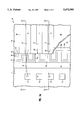
- FIG. 1 shows a portion of a prior art substrate 10 including a mounted die 11, bond pads 12 on die 11, a first bus 13, a second bus 14, and package leads 15.
- the buses 13 and 14 and leads 15 are all formed in one conductor level.
- each bus is shown by the arrows 16.
- the leads 15 are moved outward from the die 11, by a distance shown by the arrow 17, to provide room for the buses.
- the arrow 17 extends from the edge 18 on the die side of the bus 13 to the end 15a of a lead 15.
- the conductors, such as bond wires 19, that connect pads 12 to leads 15, are longer by the amount shown by arrow 17 than they would be in the absence of buses.
- Other bond wires 19 are shown connecting, a pad 12 to the bus 14, a lead 15 to the bus 13, and a lead 15 to the bus 14, in accordance with the discussion above.
- two buses have been provided in an integrated circuit package, one bus being in one conductor level and the other bus being in another conductor level.
- the exposed areas of the buses are parallel streets, located between the die and the leads, and separated at least vertically from each other and laterally from the die and from the leads.
- the buses increase the distance from pads to leads by the distance from the die side of the inner bus to the lead, that is to say by the width of the two buses and by the width of the separation between bus and leads.
- each bus must be at least wide enough for wire or TAB or other suitable connection.
- the increased distance between pads and leads requires longer wire or TAB connections.
- the longer connections have larger inductance which causes stronger magnetic coupling and associated electrical noise.
- One particularly troublesome example of this, called “ground bounce”, is associated with simultaneous switching of a number of output buffers, and is proportional to the total inductance present.
- a goal of the present invention is to provide two buses in a single level of conductor while minimizing the disadvantages described above.
- the present invention provides a compact arrangement of two buses for use with an integrated circuit die.
- the buses are located in the interconnect area outside the die attach area and have a special geometry described as follows.
- the buses formed in a single conductor level, are in the form of two opposing combs, with each comb having a ribbon portion and fingers extending from the ribbon portion, and with the fingers of one comb located between the fingers of the other comb in a so-called interdigitated configuration.
- the first bus located closest to the integrated circuit die, includes a ribbon portion close to the die with attached fingers pointing away from the die towards the second bus.
- the second bus includes a ribbon portion having fingers attached, the fingers pointing towards the integrated circuit die and falling between the oppositely pointing fingers of the first bus.
- Pads and leads may be connected to the fingers by wire bonding or by other conventional means.
- the ribbon portion connects the fingers together to provide electrical continuity.
- One die design may be replaced by another having different pad numbers assigned to a given fixed voltage merely by altering the list of pads to be connected to fingers on the appropriate bus.
- the width of two comb buses can be compared to the width of two street buses as follows.
- the minimum width of either type of bus is the same and is that required to accommodate wire connections or TAB connections or other appropriate connections.
- the sum of the widths of two comb buses in interdigitated configuration is, however, less than the sum of the widths of two street buses.
- the difference is equal to the difference between a street bus and the ribbon portion of a comb bus.
- the ribbon portion of a comb bus does not have to accommodate wire or TAB or other connections and is therefore narrower than a street bus.
- connection distances between lead and pad, between lead and inner bus and between pad and outer bus are all reduced by an amount equal to the change in width of the two buses.
- connection distances between the outer bus and leads and between outer bus and pads are reduced by an amount equal to the change in the width of two buses.
- FIG. 1 shows, in plan outline, a portion of a substrate having two buses and leads in a single conductor level, according to the prior art.
- FIG. 2 shows, in plan outline, a portion of a substrate having two interdigitated comb buses and leads in a single conductor level, in accordance with the present invention.
- FIG. 3A shows, in plan outline, a portion of an integrated circuit assembly having two conductor levels and having interdigitated comb buses in accordance with the present invention.
- FIG. 3B shows a cross section taken at 3B--3B of FIG. 3A
- FIG. 3C shows a cross section taken at 3C--3C of FIG. 3A.
- FIG. 4 shows a schematic perspective and section view of an integrated circuit package in accordance with the present invention.
- FIG. 2 shows a portion of an integrated circuit assembly 20 in accordance with the present invention.
- the assembly 20 includes an insulative substrate 91, an integrated circuit die 11, mounted thereon and having a peripheral edge 11a, bond pads 12 adjacent to the edge of the die 11, a first comb bus 23 on the substrate 91, a second comb bus 24 on the substrate 91 interdigitated with the first bus 23, and leads 15 on the substrate 91.
- the buses and leads are all formed in a single conductor level deposited on or laminated to the substrate and etched or patterned, all by conventional methods.
- the interdigitated fingers 23b and 24b of the combs extend laterally from strips 23a and 24a respectively. The width of each bus is shown by the arrows 26.
- the leads 15 are moved outward from the die 11, by a distance shown by the arrow 27, to provide room for the buses.
- the conductors, such as bond wires 29, that connect bond pads 12 to leads 15 are longer by the length of arrow 27 than they would be without buses.
- the arrow 27 extends from the edge 18 on the die side of the bus 23 to the end 15a of a lead 15.
- the arrow 27 in FIG. 2 is shorter than the arrow 17 in FIG. 1 by the length of arrow 28.
- the arrows 28 show how far certain features, for example, the end 15a of leads 15, are displaced back toward the die from the positions of the same features in FIG. 1, as a result of changing from street buses of FIG. 1 to the interdigitated comb buses of FIG. 2.
- the bond wires 29 that connect pads 12 to leads 15, pads 12 to bus 24, and bus 23 to leads 15 are all shorter in FIG. 2, by the length of arrow 28, than they are in FIG. 1.
- FIG. 3A shows a portion of an integrated circuit assembly 30 in accordance with the present invention.
- FIGS. 3B and 3C show cross sections taken at 3B--3B and at 3C--3C, respectively.
- the assembly 30 includes a substrate-mounted die 11 on substrate 91, bond pads 12 adjacent a die peripheral edge 11a, a first comb bus 33, a second comb bus 34, and leads 15.
- the buses 33 and 34 are in a first level of conductor 92 on the substrate 91.
- a first level of insulator 80 extends from line 81 over the entire area to the right of line 81.
- the first level of insulator 80 is absent to the left of line 81 and is shown cut away for clarity in the lower right portion of FIG. 3A.
- the first level of insulator 80 is above the first level of conductor 92 and below a second level of conductor 93.
- the leads 15 are in the second level of conductor 93 and overlie the first level of insulator 80.
- the leads 15 are not laterally separated from buses 33 and 34. They are vertically separated from buses 33 and 34 by first insulator level 80. This configuration (buses in a first conductor level and leads in a second conductor level) allows closer spacing of the leads 15 to the pads 12.
- the insulator 80 overlies the strip 34a and a portion of finger 33b in the cross section shown in FIG. 3B. It should be noted that the spacing of leads to pads shown in FIG.
- the buses 33 and 34 can be maintained without having the leads 15 or first insulator 80 overlying any portion of the buses 33 and 34.
- the ribbon portion 34a of bus 34 is outside the area covered by first insulator level 80, as shown in the upper portion of FIG. 3A and in FIG. 3C.
- the buses may be extended to any required distance to the right of line 81 under insulator 80, as shown in the lower portion of FIG. 3A, i.e. the edge 34d of bus 34 may be moved further to the right.
- the width 17a of the exposed portions of the two buses to the left of line 81 in FIGS. 3A, 3B and 3C is the same as the width 17a of the two buses in FIG. 2.
- FIG. 3A The extent to which the use of a second level of conductor allows the ends of the leads to be moved from their former positions in FIG. 2 closer to the pads 12 is shown in FIG. 3A by the arrows 38.
- the distances between leads 15 and bus 34, between leads 15 and bus 33, and between leads 15 and pads 12 are also reduced by the distance represented by arrow 38.
- the lengths of conductors, such as bond wires 39, required to connect leads 15 to bus 34, leads 15 to bus 33, and leads 15 to pads 12 are also reduced by that amount, i.e. the length of arrow 38.
- the bond wire 39 connecting a lead 15 to a pad 12 and the bond wire 39 connecting a lead 15 to the bus 33 are shorter in FIG. 3A than in FIG. 1 by an amount equal to the sum of the lengths of the arrow 28 in FIG. 2 and the arrow 38 in FIG. 3.
- the leads 15 may be laterally separated from buses 33 an 34 in FIG. 3 at the cost of moving the leads 15 further away from the pads 12.
- Plated vias or filled vias may be used to connect the two levels of conductor shown in FIGS. 3A, 3B and 3C to other conductor levels not shown.
- FIG. 4 shows a perspective view and section of portion 40 of an integrated circuit package.
- the embodiment shown in FIG. 4 is similar to that shown in plan outline in FIG. 3A (i.e. the buses are in one conductor level and the leads are in another conductor level).
- the portion 40 includes die 11 attached to a substrate 91, bond pads 12 on the die, a first comb bus 43, a second comb bus 44, and leads 15.
- the buses 43 and 44 are in a first level of conductor 92.
- a first level of insulator 80 lies on top of the first level of conductor 92.
- the leads 15 are in a second level of conductor 93 on top of the first level of insulator 80.
- the first level of insulator 80 overlies portions of the bus 44 (i.e. strip 44a which connects fingers 44b together).
- This embodiment can be modified so that the fingers 43b of bus 43 are also partly overlaid by first insulator level 80 (as in the lower part of FIG. 3A).
- the leads 15 are vertically separated but not laterally separated from bus 44 by the first insulator level 80.
- the outer boundary 44d of bus 44 can be moved out from under insulator 80 so that the insulator 80 and leads 15 do not overlay any part of the buses (as in the upper part of FIG. 3A and in FIG. 3C).
- buses 43 and 44 (strip 43a and interdigitated fingers 43b and 44b, exposed by an opening 101 in the insulator 80) must be at least sufficient to receive wire bond or other connections.
- a third conductor level 94 and a third insultator level 100 are shown in FIG. 4. Plated or other vias 95 are shown connecting bus 43 to third conductor level 94. Additional conductor levels can be added to the structure. Buses 43 and 44 can be connected by conductive vias to these other conductor levels as appropriate.
- the buses substantially circle the die attach area 97 although for clarity, only three sides of the buses are shown around die 11.
- the structure is similar to that shown in FIG. 4 except that the positions of buses and leads are reversed, the leads being in the first conductor level 92 rather than in the second conductor level 93 and the exposed portions of the leads being between the buses and the die.
- two interdigitated comb buses may be implemented in one conductor level and an additional two interdigitated comb buses may be implemented in another conductor level so that a die attach area is partly or completely encircled by these four buses.
- a bus may be at any voltage required. Two buses in a pair may be at different voltages or at the same voltage. For example, many high speed circuits have a "clean" power for the core circuitry and a “dirty” or “noisy” power for the input/output circuitry. Likewise, in a pair of interdigitated buses, one may be for "clean” ground and the other for "dirty” ground.
- any number of conductor levels may be used. Additional conductor levels may exist above or below a conductor level or levels containing the buses. Either one or both of the buses may be extended to form a ground or power plane. Either one or both of the buses may be connected by vias to other conductor levels. The bus closest to the die may be an extension of a conductive layer covering the die attach area.
Abstract
Description
Claims (6)
Priority Applications (1)
| Application Number | Priority Date | Filing Date | Title |
|---|---|---|---|
| US08/688,083 US5672909A (en) | 1995-02-07 | 1996-07-29 | Interdigitated wirebond programmable fixed voltage planes |
Applications Claiming Priority (2)
| Application Number | Priority Date | Filing Date | Title |
|---|---|---|---|
| US38502495A | 1995-02-07 | 1995-02-07 | |
| US08/688,083 US5672909A (en) | 1995-02-07 | 1996-07-29 | Interdigitated wirebond programmable fixed voltage planes |
Related Parent Applications (1)
| Application Number | Title | Priority Date | Filing Date |
|---|---|---|---|
| US38502495A Continuation | 1995-02-07 | 1995-02-07 |
Publications (1)
| Publication Number | Publication Date |
|---|---|
| US5672909A true US5672909A (en) | 1997-09-30 |
Family
ID=23519725
Family Applications (1)
| Application Number | Title | Priority Date | Filing Date |
|---|---|---|---|
| US08/688,083 Expired - Lifetime US5672909A (en) | 1995-02-07 | 1996-07-29 | Interdigitated wirebond programmable fixed voltage planes |
Country Status (1)
| Country | Link |
|---|---|
| US (1) | US5672909A (en) |
Cited By (20)
| Publication number | Priority date | Publication date | Assignee | Title |
|---|---|---|---|---|
| US5825084A (en) * | 1996-08-22 | 1998-10-20 | Express Packaging Systems, Inc. | Single-core two-side substrate with u-strip and co-planar signal traces, and power and ground planes through split-wrap-around (SWA) or split-via-connections (SVC) for packaging IC devices |
| US5903050A (en) * | 1998-04-30 | 1999-05-11 | Lsi Logic Corporation | Semiconductor package having capacitive extension spokes and method for making the same |
| US6043559A (en) * | 1996-09-09 | 2000-03-28 | Intel Corporation | Integrated circuit package which contains two in plane voltage busses and a wrap around conductive strip that connects a bond finger to one of the busses |
| US6060778A (en) * | 1997-05-17 | 2000-05-09 | Hyundai Electronics Industries Co. Ltd. | Ball grid array package |
| US6111311A (en) * | 1997-12-26 | 2000-08-29 | Nec Corporation | Semiconductor device and method of forming the same |
| US6111313A (en) * | 1998-01-12 | 2000-08-29 | Lsi Logic Corporation | Integrated circuit package having a stiffener dimensioned to receive heat transferred laterally from the integrated circuit |
| US6121679A (en) * | 1998-03-10 | 2000-09-19 | Luvara; John J. | Structure for printed circuit design |
| US6177723B1 (en) * | 1997-04-10 | 2001-01-23 | Texas Instruments Incorporated | Integrated circuit package and flat plate molding process for integrated circuit package |
| US6310303B1 (en) | 1998-03-10 | 2001-10-30 | John J. Luvara | Structure for printed circuit design |
| US6545348B1 (en) | 1999-03-12 | 2003-04-08 | Kabushiki Kaisha Toshiba | Package for a semiconductor device comprising a plurality of interconnection patterns around a semiconductor chip |
| US20030143781A1 (en) * | 2002-01-31 | 2003-07-31 | Mclellan Neil Robert | Encapsulated integrated circuit package and method of manufacturing an integrated circuit package |
| US6608390B2 (en) | 2001-11-13 | 2003-08-19 | Kulicke & Soffa Investments, Inc. | Wirebonded semiconductor package structure and method of manufacture |
| US20030234454A1 (en) * | 2002-06-24 | 2003-12-25 | Serafin Pedron | Integrated circuit package and method of manufacturing the integrated circuit package |
| US6734552B2 (en) | 2001-07-11 | 2004-05-11 | Asat Limited | Enhanced thermal dissipation integrated circuit package |
| US7015072B2 (en) | 2001-07-11 | 2006-03-21 | Asat Limited | Method of manufacturing an enhanced thermal dissipation integrated circuit package |
| US20060148127A1 (en) * | 2004-12-31 | 2006-07-06 | Carsem Semiconductor Sdn. Bhd. | Method of manufacturing a cavity package |
| US20070187808A1 (en) * | 2006-02-16 | 2007-08-16 | Easic Corporation | Customizable power and ground pins |
| US7489519B1 (en) * | 2008-04-15 | 2009-02-10 | International Business Machines Corporation | Power and ground ring snake pattern to prevent delamination between the gold plated ring and mold resin for wirebond PBGA |
| US20110193215A1 (en) * | 2010-02-09 | 2011-08-11 | Renesas Electronics Corporation | Semiconductor package |
| US20110267789A1 (en) * | 2010-04-28 | 2011-11-03 | Advanpack Solutions Pte Ltd. | Etch-back type semiconductor package, substrate and manufacturing method thereof |
Citations (12)
| Publication number | Priority date | Publication date | Assignee | Title |
|---|---|---|---|---|
| US4410905A (en) * | 1981-08-14 | 1983-10-18 | Amp Incorporated | Power, ground and decoupling structure for chip carriers |
| US4839717A (en) * | 1986-12-19 | 1989-06-13 | Fairchild Semiconductor Corporation | Ceramic package for high frequency semiconductor devices |
| US5008734A (en) * | 1989-12-20 | 1991-04-16 | National Semiconductor Corporation | Stadium-stepped package for an integrated circuit with air dielectric |
| JPH0432252A (en) * | 1990-05-29 | 1992-02-04 | Ibiden Co Ltd | Electronic component mounting board |
| US5173767A (en) * | 1990-05-28 | 1992-12-22 | Siemens Aktiengesellschaft | Integrated circuit housing composed of three coated, dielectric plates |
| US5225709A (en) * | 1990-06-15 | 1993-07-06 | Hitachi, Ltd. | Package having a structure for stabilizing and/or impedance-matching a semiconductor IC device accommodated therein |
| US5294751A (en) * | 1990-11-15 | 1994-03-15 | Hitachi Ltd. | High frequency signal transmission line structure having shielding conductor unit |
| JPH0685154A (en) * | 1992-09-07 | 1994-03-25 | Hitachi Ltd | Semiconductor integrated circuit device |
| US5329156A (en) * | 1992-12-22 | 1994-07-12 | Spectrian, Inc. | Feed bus for RF power transistors |
| US5343074A (en) * | 1993-10-04 | 1994-08-30 | Motorola, Inc. | Semiconductor device having voltage distribution ring(s) and method for making the same |
| US5457340A (en) * | 1992-12-07 | 1995-10-10 | Integrated Device Technology, Inc. | Leadframe with power and ground planes |
| US5497031A (en) * | 1993-09-24 | 1996-03-05 | Kabushiki Kaisha Toshiba | Semiconductor device having semiconductor chip with backside electrode |
-
1996
- 1996-07-29 US US08/688,083 patent/US5672909A/en not_active Expired - Lifetime
Patent Citations (13)
| Publication number | Priority date | Publication date | Assignee | Title |
|---|---|---|---|---|
| US4410905A (en) * | 1981-08-14 | 1983-10-18 | Amp Incorporated | Power, ground and decoupling structure for chip carriers |
| US4839717A (en) * | 1986-12-19 | 1989-06-13 | Fairchild Semiconductor Corporation | Ceramic package for high frequency semiconductor devices |
| US5008734A (en) * | 1989-12-20 | 1991-04-16 | National Semiconductor Corporation | Stadium-stepped package for an integrated circuit with air dielectric |
| US5173767A (en) * | 1990-05-28 | 1992-12-22 | Siemens Aktiengesellschaft | Integrated circuit housing composed of three coated, dielectric plates |
| JPH0432252A (en) * | 1990-05-29 | 1992-02-04 | Ibiden Co Ltd | Electronic component mounting board |
| US5225709A (en) * | 1990-06-15 | 1993-07-06 | Hitachi, Ltd. | Package having a structure for stabilizing and/or impedance-matching a semiconductor IC device accommodated therein |
| US5294751A (en) * | 1990-11-15 | 1994-03-15 | Hitachi Ltd. | High frequency signal transmission line structure having shielding conductor unit |
| JPH0685154A (en) * | 1992-09-07 | 1994-03-25 | Hitachi Ltd | Semiconductor integrated circuit device |
| US5402318A (en) * | 1992-09-07 | 1995-03-28 | Hitachi, Ltd. | Semiconductor integrated circuit device |
| US5457340A (en) * | 1992-12-07 | 1995-10-10 | Integrated Device Technology, Inc. | Leadframe with power and ground planes |
| US5329156A (en) * | 1992-12-22 | 1994-07-12 | Spectrian, Inc. | Feed bus for RF power transistors |
| US5497031A (en) * | 1993-09-24 | 1996-03-05 | Kabushiki Kaisha Toshiba | Semiconductor device having semiconductor chip with backside electrode |
| US5343074A (en) * | 1993-10-04 | 1994-08-30 | Motorola, Inc. | Semiconductor device having voltage distribution ring(s) and method for making the same |
Cited By (28)
| Publication number | Priority date | Publication date | Assignee | Title |
|---|---|---|---|---|
| US5825084A (en) * | 1996-08-22 | 1998-10-20 | Express Packaging Systems, Inc. | Single-core two-side substrate with u-strip and co-planar signal traces, and power and ground planes through split-wrap-around (SWA) or split-via-connections (SVC) for packaging IC devices |
| US6043559A (en) * | 1996-09-09 | 2000-03-28 | Intel Corporation | Integrated circuit package which contains two in plane voltage busses and a wrap around conductive strip that connects a bond finger to one of the busses |
| US6440770B1 (en) | 1996-09-09 | 2002-08-27 | Intel Corporation | Integrated circuit package |
| US6177723B1 (en) * | 1997-04-10 | 2001-01-23 | Texas Instruments Incorporated | Integrated circuit package and flat plate molding process for integrated circuit package |
| US6060778A (en) * | 1997-05-17 | 2000-05-09 | Hyundai Electronics Industries Co. Ltd. | Ball grid array package |
| US6111311A (en) * | 1997-12-26 | 2000-08-29 | Nec Corporation | Semiconductor device and method of forming the same |
| US6111313A (en) * | 1998-01-12 | 2000-08-29 | Lsi Logic Corporation | Integrated circuit package having a stiffener dimensioned to receive heat transferred laterally from the integrated circuit |
| US6121679A (en) * | 1998-03-10 | 2000-09-19 | Luvara; John J. | Structure for printed circuit design |
| US6310303B1 (en) | 1998-03-10 | 2001-10-30 | John J. Luvara | Structure for printed circuit design |
| US5903050A (en) * | 1998-04-30 | 1999-05-11 | Lsi Logic Corporation | Semiconductor package having capacitive extension spokes and method for making the same |
| US6545348B1 (en) | 1999-03-12 | 2003-04-08 | Kabushiki Kaisha Toshiba | Package for a semiconductor device comprising a plurality of interconnection patterns around a semiconductor chip |
| KR100454833B1 (en) * | 1999-03-12 | 2004-11-03 | 가부시끼가이샤 도시바 | Package of Semiconductor Device |
| US6734552B2 (en) | 2001-07-11 | 2004-05-11 | Asat Limited | Enhanced thermal dissipation integrated circuit package |
| US7015072B2 (en) | 2001-07-11 | 2006-03-21 | Asat Limited | Method of manufacturing an enhanced thermal dissipation integrated circuit package |
| US6608390B2 (en) | 2001-11-13 | 2003-08-19 | Kulicke & Soffa Investments, Inc. | Wirebonded semiconductor package structure and method of manufacture |
| US20030143781A1 (en) * | 2002-01-31 | 2003-07-31 | Mclellan Neil Robert | Encapsulated integrated circuit package and method of manufacturing an integrated circuit package |
| US20050077613A1 (en) * | 2002-01-31 | 2005-04-14 | Mclellan Neil Robert | Integrated circuit package |
| US6790710B2 (en) | 2002-01-31 | 2004-09-14 | Asat Limited | Method of manufacturing an integrated circuit package |
| US20030234454A1 (en) * | 2002-06-24 | 2003-12-25 | Serafin Pedron | Integrated circuit package and method of manufacturing the integrated circuit package |
| US6940154B2 (en) | 2002-06-24 | 2005-09-06 | Asat Limited | Integrated circuit package and method of manufacturing the integrated circuit package |
| US20060148127A1 (en) * | 2004-12-31 | 2006-07-06 | Carsem Semiconductor Sdn. Bhd. | Method of manufacturing a cavity package |
| US7273767B2 (en) | 2004-12-31 | 2007-09-25 | Carsem (M) Sdn. Bhd. | Method of manufacturing a cavity package |
| US20070187808A1 (en) * | 2006-02-16 | 2007-08-16 | Easic Corporation | Customizable power and ground pins |
| US7489519B1 (en) * | 2008-04-15 | 2009-02-10 | International Business Machines Corporation | Power and ground ring snake pattern to prevent delamination between the gold plated ring and mold resin for wirebond PBGA |
| US20110193215A1 (en) * | 2010-02-09 | 2011-08-11 | Renesas Electronics Corporation | Semiconductor package |
| US20110267789A1 (en) * | 2010-04-28 | 2011-11-03 | Advanpack Solutions Pte Ltd. | Etch-back type semiconductor package, substrate and manufacturing method thereof |
| US8917521B2 (en) * | 2010-04-28 | 2014-12-23 | Advanpack Solutions Pte Ltd. | Etch-back type semiconductor package, substrate and manufacturing method thereof |
| US9305868B2 (en) | 2010-04-28 | 2016-04-05 | Advanpack Solutions Pte Ltd. | Manufacturing method of forming an etch-back type semiconductor package with locking anchorages |
Similar Documents
| Publication | Publication Date | Title |
|---|---|---|
| US5672909A (en) | Interdigitated wirebond programmable fixed voltage planes | |
| CA1201820A (en) | Semiconductor integrated circuit including a lead frame chip support | |
| US5386141A (en) | Leadframe having one or more power/ground planes without vias | |
| US5373188A (en) | Packaged semiconductor device including multiple semiconductor chips and cross-over lead | |
| US4945399A (en) | Electronic package with integrated distributed decoupling capacitors | |
| US5138430A (en) | High performance versatile thermally enhanced IC chip mounting | |
| US5473514A (en) | Semiconductor device having an interconnecting circuit board | |
| US20060118924A1 (en) | Lead frame assemblies and decoupling capacitors | |
| KR100328906B1 (en) | Method and device for joining leads inside lead-on chip of leadframe | |
| EP0645811B1 (en) | Semiconductor device having semiconductor chip with backside electrode | |
| JPH0582585A (en) | Semiconductor device | |
| GB2306775A (en) | integrated circuit package | |
| JPH0587977B2 (en) | ||
| US5311058A (en) | Integrated circuit power distribution system | |
| JP3154579B2 (en) | Lead frame for mounting semiconductor elements | |
| US7288846B2 (en) | Semiconductor chip having pads with plural junctions for different assembly methods | |
| US5164817A (en) | Distributed clock tree scheme in semiconductor packages | |
| US7466021B2 (en) | Memory packages having stair step interconnection layers | |
| EP0307722A1 (en) | Semiconductor device having improved multilayered wirings | |
| US8258607B2 (en) | Apparatus and method for providing bypass capacitance and power routing in QFP package | |
| GB2289985A (en) | Connecting the output pads on an i.c. chip, using an adaptor board | |
| US5751057A (en) | Lead on chip lead frame design without jumpover wiring | |
| JPS5854661A (en) | Multilayer ceramic semiconductor package | |
| WO1996004682A1 (en) | Electronic circuit package | |
| EP0394878B1 (en) | Semiconductor device having multi-layered wiring structure |
Legal Events
| Date | Code | Title | Description |
|---|---|---|---|
| STCF | Information on status: patent grant |
Free format text: PATENTED CASE |
|
| AS | Assignment |
Owner name: GUARDIAN ASSETS, INC., PENNSYLVANIA Free format text: SECURITY INTEREST;ASSIGNOR:AMKOR TECHNOLOGY, INC.;REEL/FRAME:011122/0773 Effective date: 20000428 |
|
| AS | Assignment |
Owner name: SOCIETE GENERALE, NEW YORK Free format text: RE-RECORD TO CORRECT RECEIVING PARTY NAME ON A DOCUMENT PREVIOUSLY RECORDED ON REEL 011122, FRAME 0773.;ASSIGNORS:AMKOR TECHNOLOGY, INC.;GUARDIAN ASSETS, INC.;REEL/FRAME:011457/0702 Effective date: 20000428 |
|
| FPAY | Fee payment |
Year of fee payment: 4 |
|
| AS | Assignment |
Owner name: CITICORP USA, INC., NEW YORK Free format text: SECURITY INTEREST;ASSIGNORS:SOCIETE GENERALE;GUARDIAN ASSETS, INC.;REEL/FRAME:011682/0416 Effective date: 20010330 |
|
| AS | Assignment |
Owner name: CITICORP NORTH AMERICA, INC. AS ADMINISTRATIVE AGE Free format text: SECURITY AGREEMENT;ASSIGNORS:AMKOR TECHNOLOGY, INC.;GUARDIAN ASSETS, INC.;REEL/FRAME:014885/0691 Effective date: 20040629 |
|
| AS | Assignment |
Owner name: AMKOR TECHNOLOGY, INC., PENNSYLVANIA Free format text: RELEASE OF LIEN ON PATENTS;ASSIGNOR:CITICORP USA, INC. AS COLLATERAL AGENT;REEL/FRAME:015603/0572 Effective date: 20040629 |
|
| AS | Assignment |
Owner name: CITICORP NORTH AMERICA, INC. AS "AGENT", NEW YORK Free format text: SECURITY AGREEMENT;ASSIGNORS:AMKOR TECHNOLOGY, INC.;GUARDIAN ASSETS, INC.;REEL/FRAME:015942/0521 Effective date: 20041027 |
|
| FEPP | Fee payment procedure |
Free format text: PAYOR NUMBER ASSIGNED (ORIGINAL EVENT CODE: ASPN); ENTITY STATUS OF PATENT OWNER: LARGE ENTITY |
|
| FPAY | Fee payment |
Year of fee payment: 8 |
|
| AS | Assignment |
Owner name: AMKOR TECHNOLOGY, INC., ARIZONA Free format text: TERMINATION & RELEASE OF PATENT SECURITY AGREEMENT;ASSIGNOR:CITICORP NORTH AMERICA, INC.;REEL/FRAME:017388/0868 Effective date: 20051128 Owner name: BANK OF AMERICA, N.A., TEXAS Free format text: SECURITY AGREEMENT;ASSIGNOR:AMKOR TECHNOLOGY, INC.;REEL/FRAME:017379/0630 Effective date: 20051123 |
|
| FPAY | Fee payment |
Year of fee payment: 12 |
|
| AS | Assignment |
Owner name: BANK OF AMERICA, N.A., AS AGENT, CALIFORNIA Free format text: SECURITY INTEREST;ASSIGNOR:AMKOR TECHNOLOGY, INC.;REEL/FRAME:046683/0139 Effective date: 20180713 |
|
| AS | Assignment |
Owner name: AMKOR TECHNOLOGY SINGAPORE HOLDING PTE.LTD., SINGAPORE Free format text: ASSIGNMENT OF ASSIGNORS INTEREST;ASSIGNOR:AMKOR TECHNOLOGY, INC.;REEL/FRAME:054036/0599 Effective date: 20191119 |