US5700046A - Wafer gripper - Google Patents
Wafer gripper Download PDFInfo
- Publication number
- US5700046A US5700046A US08/527,796 US52779695A US5700046A US 5700046 A US5700046 A US 5700046A US 52779695 A US52779695 A US 52779695A US 5700046 A US5700046 A US 5700046A
- Authority
- US
- United States
- Prior art keywords
- wafer
- gripping member
- gripping
- contactor elements
- gripper assembly
- Prior art date
- Legal status (The legal status is an assumption and is not a legal conclusion. Google has not performed a legal analysis and makes no representation as to the accuracy of the status listed.)
- Expired - Lifetime
Links
Images


Classifications
-
- B—PERFORMING OPERATIONS; TRANSPORTING
- B25—HAND TOOLS; PORTABLE POWER-DRIVEN TOOLS; MANIPULATORS
- B25J—MANIPULATORS; CHAMBERS PROVIDED WITH MANIPULATION DEVICES
- B25J15/00—Gripping heads and other end effectors
- B25J15/02—Gripping heads and other end effectors servo-actuated
- B25J15/0253—Gripping heads and other end effectors servo-actuated comprising parallel grippers
- B25J15/026—Gripping heads and other end effectors servo-actuated comprising parallel grippers actuated by gears
-
- H—ELECTRICITY
- H01—ELECTRIC ELEMENTS
- H01L—SEMICONDUCTOR DEVICES NOT COVERED BY CLASS H10
- H01L21/00—Processes or apparatus adapted for the manufacture or treatment of semiconductor or solid state devices or of parts thereof
- H01L21/67—Apparatus specially adapted for handling semiconductor or electric solid state devices during manufacture or treatment thereof; Apparatus specially adapted for handling wafers during manufacture or treatment of semiconductor or electric solid state devices or components ; Apparatus not specifically provided for elsewhere
- H01L21/683—Apparatus specially adapted for handling semiconductor or electric solid state devices during manufacture or treatment thereof; Apparatus specially adapted for handling wafers during manufacture or treatment of semiconductor or electric solid state devices or components ; Apparatus not specifically provided for elsewhere for supporting or gripping
- H01L21/687—Apparatus specially adapted for handling semiconductor or electric solid state devices during manufacture or treatment thereof; Apparatus specially adapted for handling wafers during manufacture or treatment of semiconductor or electric solid state devices or components ; Apparatus not specifically provided for elsewhere for supporting or gripping using mechanical means, e.g. chucks, clamps or pinches
- H01L21/68707—Apparatus specially adapted for handling semiconductor or electric solid state devices during manufacture or treatment thereof; Apparatus specially adapted for handling wafers during manufacture or treatment of semiconductor or electric solid state devices or components ; Apparatus not specifically provided for elsewhere for supporting or gripping using mechanical means, e.g. chucks, clamps or pinches the wafers being placed on a robot blade, or gripped by a gripper for conveyance
-
- Y—GENERAL TAGGING OF NEW TECHNOLOGICAL DEVELOPMENTS; GENERAL TAGGING OF CROSS-SECTIONAL TECHNOLOGIES SPANNING OVER SEVERAL SECTIONS OF THE IPC; TECHNICAL SUBJECTS COVERED BY FORMER USPC CROSS-REFERENCE ART COLLECTIONS [XRACs] AND DIGESTS
- Y10—TECHNICAL SUBJECTS COVERED BY FORMER USPC
- Y10S—TECHNICAL SUBJECTS COVERED BY FORMER USPC CROSS-REFERENCE ART COLLECTIONS [XRACs] AND DIGESTS
- Y10S294/00—Handling: hand and hoist-line implements
- Y10S294/902—Gripping element
-
- Y—GENERAL TAGGING OF NEW TECHNOLOGICAL DEVELOPMENTS; GENERAL TAGGING OF CROSS-SECTIONAL TECHNOLOGIES SPANNING OVER SEVERAL SECTIONS OF THE IPC; TECHNICAL SUBJECTS COVERED BY FORMER USPC CROSS-REFERENCE ART COLLECTIONS [XRACs] AND DIGESTS
- Y10—TECHNICAL SUBJECTS COVERED BY FORMER USPC
- Y10S—TECHNICAL SUBJECTS COVERED BY FORMER USPC CROSS-REFERENCE ART COLLECTIONS [XRACs] AND DIGESTS
- Y10S414/00—Material or article handling
- Y10S414/135—Associated with semiconductor wafer handling
- Y10S414/141—Associated with semiconductor wafer handling includes means for gripping wafer
Definitions
- the invention relates to a gripper mechanism for semiconductor wafers.
- the wafer is supported on a chuck, and a plurality of moveable stops are disposed with even angular spacing around the center of the chuck.
- the stops are moveable radially towards and away from the center thereby to clamp the periphery of a wafer located on the chuck.
- the centering mechanism does not perform a transporting function and further involves a complicated mechanism to facilitate the simultaneous radial movement of the six stops.
- a wafer gripper assembly comprising a first gripping member having a first gripping face with a plurality of contactor elements thereon; a second gripping member having a second gripping face with a plurality of contactor elements thereon, the second gripping face opposing the first gripping face, wherein the gripping members are movably mounted for linear movement towards and away from each other; and a motor connected to both gripping members by a rotary-to-linear movement translator.
- the assembly typically further comprises coupling means that include a rack connected to each gripping member, and a common pinion engaging each rack to produce equal and opposite linear movement in the racks when the pinion is rotated, the motor being connected to the pinion for rotating the pinion.
- the assembly preferably includes six contactor elements. These may be distributed to define three contactor elements on each gripping member or two contactor elements on one gripping member, and four contactor elements on the other gripping member.
- the contactor elements can include a vertically extending portion having an inwardly facing convex surface for contacting an edge of a wafer, and an inwardly extending flange for supporting a lower surface of the wafer.
- a wafer gripper assembly comprising: a first gripping member; an opposing, second gripping member mounted on a support arm to oppose the first gripping member, the second gripping member being linearly movable towards and away from the first gripping member; and a motor connected to the second gripping member, wherein at least six contactor elements are defined on the gripping members.
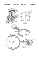
- FIG. 1 is a wafer processing robot that includes a pair of wafer gripper assemblies in accordance with the invention
- FIG. 2 is an isometric view of a wafer gripper assembly in accordance with the invention
- FIG. 3 is a schematic representation of a wafer and four gripper contact points
- FIG. 4 is a plan view of the wafer gripper assembly of FIG. 2;
- FIG. 5 is a plan view of another embodiment of the wafer gripper assembly showing the gripper assembly in its open state with a wafer located between its gripping members;
- FIG. 6 is a plan view of the gripper assembly of FIG. 5 showing the gripping members gripping a silicon wafer;
- FIG. 7 is a side view of the gripper assembly and wafer of FIG. 6;
- FIG. 8 is a plan view of the gripper assembly of FIG. 5 with the cover of the gripper housing removed;
- FIG. 9 is a partially exploded plan view of the assembly of FIG. 8;
- FIG. 10 is a schematic representation of the contactor elements of the gripper assembly of FIG. 5 showing the distribution relative to the constraints provided by a chuck;
- FIG. 11 is an isometric view of a contactor element forming part of the gripper assembly
- FIG. 12 is an isometric view of a portion of a gripping member showing a contactor element secured thereto;
- FIG. 13 is a side view of the contactor element of FIG. 11;
- FIG. 14 is a plan view of the contactor element of FIG. 13;
- FIG. 15 is a plan view of a gripping member with three contactor elements forming part of the embodiment illustrated in FIG. 5;
- FIG. 16 is yet another embodiment of a gripper assembly in accordance with the invention.
- FIG. 17 is a schematic plan view of a semiconductor wafer cassette showing the relative locations of the contactor elements of the assembly of FIG. 16.
- the present wafer gripper assembly has been developed to perform the centering operation when the wafer is picked up by the wafer handling robot. This saves space and reduces overall machine complexity.
- the various embodiments of the invention make use of a plurality of contactor elements. This centers the wafer with a degree of accuracy which exceeds the allowable tolerance on the wafer diameter. Specifically, target centering accuracy for the gripper assembly is better than 0.04 millimeters. Theoretically only three contact points are required to achieve accurate centering of a round wafer.
- the present invention envisages the use of a larger number of contact points. Specifically, at least six contactor elements are used. This has the advantage that the centering operation is insensitive to the location of flat sections or notches on the wafer. The position of the contact points can be optimized for maximum centering accuracy bearing in mind the geometric constraints imposed by either a wafer chuck or a wafer holding cassette.
- a further concept applied in a number of the embodiments of the present invention is that of coupled linear motion of the gripping members, which will be described in greater detail below. It essentially comprises the simultaneous movement in opposite directions of both gripping elements to maintain a fixed center point at all times.
- FIG. 1 illustrates a wafer handling robot 10 which includes two "fork” grippers 12 in accordance with the invention.
- each gripper assembly comprises a pair of gripping members 14, each having a semicircular shape and a linear portion 15 extending into a housing 16.
- Three contactor elements 18 protrude inwardly from each of the gripping members 14 and serve to support and center a wafer between them. By using a total of six contactor elements, greater centering accuracy of a wafer can be achieved.
- FIG. 3 shows a four-contact-point arrangement used in handling a typical wafer. The contact points 19 exert an inward force on the edges of the wafer 20. If the flat portion 21 of the wafer 20 coincides with one of the contact points 19, as shown, a net force is exerted on the wafer 19, as indicated by the arrow 22. This makes the arrangement more susceptible to errors.
- FIG. 4 shows the assembly in plan view with the cover of the housing 16 removed.
- the straight portions 15 of the gripping members are each secured to a rack 23, 24.
- the racks 23, 24 are coupled to a common pinion 25 that is mounted on an axle extending parallel to the straight portions 15.
- the rack 23 abuts the pinion 25 from below, while the rack 23 abuts the pinion 25 from above.
- Rotation of the pinion 25 by means of a motor 26 thus causes linear movement of the portions 15 towards and away from each other by equal and opposite distances.
- the geometric center 30 of the silicon wafer 32 gripped by the gripper assembly 12 does not move relative to the housing 16.
- FIGS. 5 to 7 illustrate another embodiment of the invention. Once again this a "fork" gripper.
- FIG. 5 shows the gripper assembly 40 in its open state with a wafer 42 located between its gripping members 44.
- the gripping members 44 each comprises a plate defining a semicircular section 46. This plate construction provides a sturdier arrangement than the embodiment illustrated in FIG. 4.
- holes 48 are provided in the plates.
- FIG. 6 shows the gripper assembly of FIG. 5 in a gripping state in which the gripping members 44 have been moved together to grip the wafer 42 by means of six contactor elements 50.
- the plates When viewed from the side, as illustrated in FIG. 7, it is seen that the plates define an elbow 52 at the housing 54 so as to enter the housing 54 near its top. This allows a motor to be mounted with a vertical axle as described in greater detail with reference to FIG. 8.
- FIG. 8 shows the gripper assembly 40 with the housing cap of the housing 54, removed.
- the one gripping member which for ease of reference will be indicated by reference numeral 56, is connected to a rack 58.
- the other gripping member 60 is connected to a second rack 62.
- a vertically extending pinion 64 couples the racks 58, 62 to a common drive motor (not shown) having a vertically extending shaft 68.
- rotation of the pinion causes linear movement of the racks in opposite directions, thereby maintaining a fixed geometric center.
- FIG. 9 shows a partially exploded view of the assembly of FIG. 8 to, further, expose the drive mechanism of the gripper assembly 40.
- the gripping member 56 extends into a connector plate 70 which is secured by conventional means to a bearing block 72.
- the bearing block 72 rides on a bearing track 74 to provide the linear movement mentioned above.
- the gripping member 60 extends into a connector plate 76 which is secured by conventional means to a bearing block 78.
- the bearing block 78 also rides on the bearing track 74.
- the use of a common track 74 for the two bearing blocks 72, 78 ensures parallel movement of the bearing blocks 72, 78.
- a return spring 82 is secured with one end to the housing 54 and at its other end to the connector plate 76, as illustrated in FIG. 8. The return spring 82 urges the member 60 to its closed position. Since the members 56, 60 are coupled to one another by means of the pinion 64, the member 56 is clearly also urged to its closed position.
- the gripper assembly is typically used to transfer a wafer to and from a rotary chuck (not shown). For instance, a wafer is lowered onto a chuck by positioning the wafer over the chuck and lowering the vertically extending robot cylinder 90, thereby positioning the wafer on the chuck. Similarly, the wafer is removed by moving the gripping member in underneath the wafer and lifting the wafer off the chuck. It will be appreciated that, in both cases, the free ends of the gripping members have to clear the chuck. It is therefore essential that the grippers be capable of sufficient linear movement to accommodate the diameter of the chuck. This is illustrated in FIG. 10, in which the lines 92 represent the constraints presented by the chuck.
- the contactor elements are represented by the circles 94 and, as can be seen from FIG. 10, the contactor elements 96, which are secured near the free ends of the gripping members, are positioned so as to clear the chuck when the gripping members are in their closed state.
- FIG. 11 illustrates a contactor element 50 in greater detail. It comprises a base 98 and an upwardly extending semi-cylindrical portion 100.
- the semi-cylindrical portion 100 defines a convex surface 102 for contacting the edge of a wafer.
- the inwardly extending portion 104 of the base 98 constitutes a flange for supporting the lower surface of a wafer, while the outwardly extending portion 106 of the base 98 serves as a securing formation for securing the element 50 to a gripping member as illustrated in FIGS. 12 to 14.
- the semicircular portions of the gripping members 44 are provided with recesses for complimentarily receiving the portions 106 and part of the semi-cylindrical portions 100 of the elements 50.
- FIG. 13 shows the contactor element 50 from the side.
- a bore 110 extends through the portion 106, as is also illustrated in the plan view of FIG. 14.
- three contactor elements 50 are placed in complimentary recesses in each gripping member 44 so as to extend inwardly as illustrated in FIG. 15.
- the contactor elements 50 are secured by means of screws (not shown) extending through the portions 106 into the gripping member 44.
- FIG. 16 shows another embodiment of a gripper assembly in accordance with the invention.
- the gripper assembly 200 is referred to as a "tongue" gripper and is used to move wafers into and out of cassettes.
- the cassette geometry requires that the gripper 200 be sufficiently narrowed to pass into the cassette. Instead of lateral movement, as described for the "fork" gripper of FIGS. 4 to 8, linear movement takes place along the longitudinal axis of the assembly 200.
- the gripper assembly 200 defines a plate-like first gripping member 202 and a semi-circular second gripping member 204.
- the members 202, 204 are moveable relative to the housing 206 so as to be moveable towards and away from each other. This is illustrated in FIG.
- the gripping members 202 and 204 are connected to connector plates (not shown) which connect the members 202, 204 to racks, so as to be moveable by a common pinion (not shown).
- the gripping member 204 is secured to the housing 206, and only the member 202 moves relative to the housing 206.
- the dimensions of the "tongue" gripper have to be such that it can be passed into a wafer cassette. This is illustrated in FIG. 17 in which the contactor elements 210 are indicated by circles. Once again, six contactor elements are provided to accurately center the wafer on the element 202. In the "tongue" gripper of FIGS.
- the contactor elements are not evenly distributed between the elements 202 and 204.
- the element 202 provides only two contactor elements 210, while the element 204 has four elements 210 secured thereto. This allows the narrow element 202 to be passed underneath the wafer 212 to the far end 214 of the cassette 216 without interfering with the closely spaced ends 218 of the side walls of the cassette 216.
- the fact that the contactor element indicated by reference numeral 220 coincides with the flat surface 222 of the wafer 212, does not interfere with the accurate centering of the wafer.
Abstract
Description
Claims (8)
Priority Applications (3)
| Application Number | Priority Date | Filing Date | Title |
|---|---|---|---|
| US08/527,796 US5700046A (en) | 1995-09-13 | 1995-09-13 | Wafer gripper |
| AU72382/96A AU7238296A (en) | 1995-09-13 | 1996-09-13 | Wafer gripper |
| PCT/US1996/014678 WO1997010082A1 (en) | 1995-09-13 | 1996-09-13 | Wafer gripper |
Applications Claiming Priority (1)
| Application Number | Priority Date | Filing Date | Title |
|---|---|---|---|
| US08/527,796 US5700046A (en) | 1995-09-13 | 1995-09-13 | Wafer gripper |
Publications (1)
| Publication Number | Publication Date |
|---|---|
| US5700046A true US5700046A (en) | 1997-12-23 |
Family
ID=24102963
Family Applications (1)
| Application Number | Title | Priority Date | Filing Date |
|---|---|---|---|
| US08/527,796 Expired - Lifetime US5700046A (en) | 1995-09-13 | 1995-09-13 | Wafer gripper |
Country Status (3)
| Country | Link |
|---|---|
| US (1) | US5700046A (en) |
| AU (1) | AU7238296A (en) |
| WO (1) | WO1997010082A1 (en) |
Cited By (100)
| Publication number | Priority date | Publication date | Assignee | Title |
|---|---|---|---|---|
| WO1999027577A1 (en) * | 1997-11-21 | 1999-06-03 | Asm America, Inc. | Substrate transfer system for semiconductor processing equipment |
| DE19802202A1 (en) * | 1998-01-22 | 1999-08-05 | Fraunhofer Ges Forschung | Disc gripper mechanism |
| US5947802A (en) * | 1997-11-05 | 1999-09-07 | Aplex, Inc. | Wafer shuttle system |
| US5957651A (en) * | 1995-06-08 | 1999-09-28 | Kokusai Electric Co., Ltd. | Substrate carrying apparatus |
| US5957764A (en) * | 1997-11-05 | 1999-09-28 | Aplex, Inc. | Modular wafer polishing apparatus and method |
| US5980195A (en) * | 1996-04-24 | 1999-11-09 | Tokyo Electron, Ltd. | Positioning apparatus for substrates to be processed |
| US6062961A (en) * | 1997-11-05 | 2000-05-16 | Aplex, Inc. | Wafer polishing head drive |
| US6068441A (en) * | 1997-11-21 | 2000-05-30 | Asm America, Inc. | Substrate transfer system for semiconductor processing equipment |
| US6089630A (en) * | 1997-12-27 | 2000-07-18 | Nsk Ltd. | Substrate transfer apparatus |
| WO2000048787A1 (en) * | 1999-02-19 | 2000-08-24 | Speedfam-Ipec Corporation | Improved arrangements for wafer polishing |
| US6109677A (en) * | 1998-05-28 | 2000-08-29 | Sez North America, Inc. | Apparatus for handling and transporting plate like substrates |
| US6117238A (en) * | 1995-11-07 | 2000-09-12 | Applied Science And Technology, Inc. | End effector assembly for inclusion in a system for producing uniform deposits on a wafer |
| EP1043123A2 (en) * | 1999-04-02 | 2000-10-11 | Applied Materials, Inc. | Buffer station on CMP system |
| US6146083A (en) * | 1997-07-04 | 2000-11-14 | Tokyo Electron Limited | Substrate transferring apparatus and substrate processing apparatus using the same |
| EP1060836A2 (en) * | 1999-06-18 | 2000-12-20 | Applied Materials, Inc. | Wafer tranfer station for a chemical mechanical polisher |
| US6164899A (en) * | 1999-04-22 | 2000-12-26 | Automated Concepts, Inc. | Disk transfer apparatus |
| US6167322A (en) * | 1998-07-10 | 2000-12-26 | Holbrooks; Orville Ray | Intelligent wafer handling system and method |
| US6183026B1 (en) * | 1999-04-07 | 2001-02-06 | Gasonics International Corporation | End effector |
| US6190103B1 (en) * | 1999-03-31 | 2001-02-20 | Gasonics International Corporation | Wafer transfer device and method |
| US6239863B1 (en) | 1999-10-08 | 2001-05-29 | Silicon Valley Group, Inc. | Removable cover for protecting a reticle, system including and method of using the same |
| US6260894B1 (en) * | 1999-05-28 | 2001-07-17 | Applied Materials, Inc. | Assembly for wafer handling system |
| US6282459B1 (en) * | 1998-09-01 | 2001-08-28 | International Business Machines Corporation | Structure and method for detection of physical interference during transport of an article |
| WO2002018107A1 (en) * | 2000-09-01 | 2002-03-07 | Asyst Technologies, Inc. | Edge grip aligner with buffering capabilities |
| US6390767B1 (en) * | 1999-03-10 | 2002-05-21 | Nova Measuring Instruments Ltd. | Positioning assembly |
| US6409453B1 (en) * | 1998-02-18 | 2002-06-25 | Applied Materials, Inc. | End effector for wafer handler in processing system |
| US20020106316A1 (en) * | 2001-02-08 | 2002-08-08 | Barry Billig | Exothermic reaction system |
| WO2002089183A2 (en) * | 2001-04-28 | 2002-11-07 | Leica Microsystems Jena Gmbh | Holding device for wafers |
| US6572320B2 (en) * | 1997-05-05 | 2003-06-03 | Semitool, Inc. | Robot for handling workpieces in an automated processing system |
| US6577382B2 (en) | 1997-12-03 | 2003-06-10 | Nikon Corporation | Substrate transport apparatus and method |
| US6578893B2 (en) * | 2000-10-02 | 2003-06-17 | Ajs Automation, Inc. | Apparatus and methods for handling semiconductor wafers |
| US6592324B2 (en) * | 2001-02-26 | 2003-07-15 | Irm, Llc | Gripper mechanism |
| US6612590B2 (en) * | 2001-01-12 | 2003-09-02 | Tokyo Electron Limited | Apparatus and methods for manipulating semiconductor wafers |
| US20030178866A1 (en) * | 2002-03-23 | 2003-09-25 | Kyung-Su Chae | Apparatus for conveying liquid crystal display panel |
| US6682113B2 (en) * | 2001-11-16 | 2004-01-27 | Applied Materials, Inc. | Wafer clamping mechanism |
| US6685422B2 (en) | 1999-03-18 | 2004-02-03 | Applied Materials Inc. | Pneumatically actuated flexure gripper for wafer handling robots |
| US6692219B2 (en) * | 2000-11-29 | 2004-02-17 | Tokyo Electron Limited | Reduced edge contact wafer handling system and method of retrofitting and using same |
| US20040041148A1 (en) * | 2002-09-03 | 2004-03-04 | Beniamin Shulman | Wafer monitoring system |
| US20040074322A1 (en) * | 1999-01-17 | 2004-04-22 | Eran Dvir | Buffer system for a wafer handling system |
| US20040166593A1 (en) * | 2001-06-22 | 2004-08-26 | Nolte David D. | Adaptive interferometric multi-analyte high-speed biosensor |
| US6828772B1 (en) * | 2000-06-14 | 2004-12-07 | Micron Technology, Inc. | Rotating gripper wafer flipper |
| US20060046376A1 (en) * | 2004-08-31 | 2006-03-02 | Hofer Willard L | Rotating gripper wafer flipper |
| US20060284434A1 (en) * | 2005-06-20 | 2006-12-21 | Yang Jong A | Substrate conveyance device for fabrication of liquid crystal display device |
| US20070023643A1 (en) * | 2005-02-01 | 2007-02-01 | Nolte David D | Differentially encoded biological analyzer planar array apparatus and methods |
| US20070081883A1 (en) * | 2005-09-29 | 2007-04-12 | Christopher Hofmeister | End effector with centering grip |
| US20070117028A1 (en) * | 2001-03-01 | 2007-05-24 | Asml Netherlands B.V. | Mask handling method, and mask and device or apparatus comprising a gripper therefor, device manufacturing method and device manufactured thereby |
| US20070147979A1 (en) * | 2005-12-22 | 2007-06-28 | Michael Rice | Substrate gripper for a substrate handling robot |
| US20070212257A1 (en) * | 2006-02-16 | 2007-09-13 | Purdue Research Foundation | In-line quadrature and anti-reflection enhanced phase quadrature interferometric detection |
| US20070216179A1 (en) * | 2004-01-23 | 2007-09-20 | Kawasaki Jukogyo Kabushiki Kaisha | Substrate Holding Device |
| US20080093022A1 (en) * | 2004-12-23 | 2008-04-24 | Alpay Yilmaz | Method for sequencing substrates |
| US20080100983A1 (en) * | 2006-10-18 | 2008-05-01 | Axcelis Technologies, Inc. | Sliding wafer release gripper / wafer peeling gripper |
| US20080131239A1 (en) * | 2006-11-15 | 2008-06-05 | Dynamic Micro Systems | Integrated gripper for workpiece transfer |
| US7390458B2 (en) | 2000-10-13 | 2008-06-24 | Irm Llc | High throughput processing system and method of using |
| US20080166210A1 (en) * | 2007-01-05 | 2008-07-10 | Applied Materials, Inc. | Supinating cartesian robot blade |
| US20080186477A1 (en) * | 2007-01-19 | 2008-08-07 | Xuefeng Wang | System with extended range of molecular sensing through integrated multi-modal data acquisition |
| US20080203636A1 (en) * | 2007-02-28 | 2008-08-28 | Vistec Semiconductor Systems Jena Gmbh | Apparatus for holding disk-like objects |
| US20090092470A1 (en) * | 2007-10-03 | 2009-04-09 | Bonora Anthony C | End effector with sensing capabilities |
| US7522282B2 (en) | 2006-11-30 | 2009-04-21 | Purdue Research Foundation | Molecular interferometric imaging process and apparatus |
| US20090101067A1 (en) * | 2005-07-08 | 2009-04-23 | Bonora Anthony C | Method and apparatus for wafer support |
| US20090143903A1 (en) * | 2004-06-11 | 2009-06-04 | Donald Blust | Automated business system and method of vending and returning a consumer product |
| US20090192626A1 (en) * | 2008-01-25 | 2009-07-30 | Depuy Products, Inc. | Constraining ring inserter |
| EP2042272A3 (en) * | 2007-09-28 | 2009-08-26 | Nidec Sankyo Corporation | Industrial robot with cam-actuated gripper |
| US20090309285A1 (en) * | 2008-06-11 | 2009-12-17 | Vistec Semiconductor Systems Jena Gmbh | Device for holding disk-shaped objects |
| US7651306B2 (en) | 2004-12-22 | 2010-01-26 | Applied Materials, Inc. | Cartesian robot cluster tool architecture |
| US7663092B2 (en) | 2005-02-01 | 2010-02-16 | Purdue Research Foundation | Method and apparatus for phase contrast quadrature interferometric detection of an immunoassay |
| US7694647B2 (en) | 2004-12-22 | 2010-04-13 | Applied Materials, Inc. | Cluster tool architecture for processing a substrate |
| US7694688B2 (en) | 2007-01-05 | 2010-04-13 | Applied Materials, Inc. | Wet clean system design |
| US7699021B2 (en) | 2004-12-22 | 2010-04-20 | Sokudo Co., Ltd. | Cluster tool substrate throughput optimization |
| US20100171823A1 (en) * | 2009-01-08 | 2010-07-08 | Masayuki Yamamoto | Alignment apparatus for semiconductor wafer |
| US7787126B2 (en) | 2007-03-26 | 2010-08-31 | Purdue Research Foundation | Method and apparatus for conjugate quadrature interferometric detection of an immunoassay |
| US7798764B2 (en) | 2005-12-22 | 2010-09-21 | Applied Materials, Inc. | Substrate processing sequence in a cartesian robot cluster tool |
| US7819079B2 (en) | 2004-12-22 | 2010-10-26 | Applied Materials, Inc. | Cartesian cluster tool configuration for lithography type processes |
| US20110001955A1 (en) * | 2002-02-22 | 2011-01-06 | Asml Holding N.V. | System and Method for Using a Two Part Cover and a Box for Protecting a Reticle |
| US7875144B2 (en) * | 2007-05-07 | 2011-01-25 | Lintec Corporation | Transferring device and transferring method |
| US7910356B2 (en) | 2005-02-01 | 2011-03-22 | Purdue Research Foundation | Multiplexed biological analyzer planar array apparatus and methods |
| US7950407B2 (en) | 2007-02-07 | 2011-05-31 | Applied Materials, Inc. | Apparatus for rapid filling of a processing volume |
| US20120128457A1 (en) * | 2010-11-24 | 2012-05-24 | Taiwan Semiconductor Manufacturing Company, Ltd. | Reconfigurable Guide Pin Design for Centering Wafers Having Different Sizes |
| US20120135148A1 (en) * | 2010-11-29 | 2012-05-31 | Tokyo Electron Limited | Substrate treatment system, substrate treatment method, and non-transitory computer storage medium |
| US20120220200A1 (en) * | 2009-09-18 | 2012-08-30 | Hiroto Fukushima | Polishing method and polishing apparatus |
| DE102011109647A1 (en) * | 2011-08-05 | 2013-02-07 | Centrotherm Thermal Solutions Gmbh & Co. Kg | Apparatus for displacing and/or pivoting of gripper used for holding disk-shaped substrates, has a specific moving unit which is controlled such that pivoting of specific support unit is caused relative to the other support unit |
| US8635784B2 (en) * | 2005-10-04 | 2014-01-28 | Applied Materials, Inc. | Methods and apparatus for drying a substrate |
| US20140219750A1 (en) * | 2011-06-23 | 2014-08-07 | Dynamic Micro Systems, Semiconductor Equipment Gmbh | Semiconductor cleaner systems and methods |
| US20140265392A1 (en) * | 2013-03-13 | 2014-09-18 | Varian Semiconductor Equipment Associates, Inc. | Wafer handling apparatus |
| WO2015013143A1 (en) * | 2013-07-22 | 2015-01-29 | Applied Materials, Inc. | An end effector for transferring a substrate |
| US20150279720A1 (en) * | 2014-03-27 | 2015-10-01 | Varian Semiconductor Equipment Associates, Inc. | End effector pads |
| DE10232080B4 (en) * | 2002-07-15 | 2015-10-01 | Integrated Dynamics Engineering Gmbh | Electrostatic gripper and method for its production |
| US9352471B1 (en) * | 2015-01-21 | 2016-05-31 | Applied Materials, Inc. | Substrate gripper apparatus and methods |
| US9536764B2 (en) | 2015-01-27 | 2017-01-03 | Lam Research Corporation | End effector for wafer transfer system and method of transferring wafers |
| US20170144313A1 (en) * | 2015-11-24 | 2017-05-25 | Hirata Corporation | Hand Member and Hand |
| US9779977B2 (en) | 2015-04-15 | 2017-10-03 | Lam Research Corporation | End effector assembly for clean/dirty substrate handling |
| US20170287767A1 (en) * | 2016-03-31 | 2017-10-05 | Shibaura Mechatronics Corporation | Substrate transfer apparatus, substrate processing apparatus, and substrate processing method |
| WO2017198875A1 (en) * | 2016-05-20 | 2017-11-23 | Andreas Hettich Gmbh & Co. Kg | Gripper |
| US9878453B2 (en) | 2005-07-08 | 2018-01-30 | Brooks Automation, Inc. | Workpiece structures and apparatus for accessing same |
| US20180261484A1 (en) * | 2015-05-19 | 2018-09-13 | Verselus, Llc | Paddle assembly for holding an object |
| WO2019161026A1 (en) * | 2018-02-15 | 2019-08-22 | Applied Materials, Inc. | Apparatus for handling various sized substrates |
| USD911986S1 (en) * | 2019-05-03 | 2021-03-02 | Raytheon Company | Handheld semiconductor wafer handling tool |
| US11020852B2 (en) | 2017-10-05 | 2021-06-01 | Brooks Automation, Inc. | Substrate transport apparatus with independent accessory feedthrough |
| CN113097104A (en) * | 2021-03-25 | 2021-07-09 | 青岛天仁微纳科技有限责任公司 | Production equipment and production method of square substrate |
| WO2022051372A1 (en) * | 2020-09-01 | 2022-03-10 | Applied Materials, Inc. | Substrate transfer devices |
| CN114433444A (en) * | 2022-04-11 | 2022-05-06 | 四川上特科技有限公司 | Material containing and transferring device for coating glass powder on wafer |
| USD997892S1 (en) * | 2019-11-28 | 2023-09-05 | Kokusai Electric Corporation | End effector for handling wafers |
Citations (26)
| Publication number | Priority date | Publication date | Assignee | Title |
|---|---|---|---|---|
| US3982627A (en) * | 1974-03-13 | 1976-09-28 | Canon Kabushiki Kaisha | Automatic wafer orienting apparatus |
| US4376482A (en) * | 1981-05-19 | 1983-03-15 | Tencor Instruments | Wafer orientation system |
| US4407627A (en) * | 1977-12-20 | 1983-10-04 | Canon Kabushiki Kaisha | Automatic wafer orienting apparatus |
| US4457664A (en) * | 1982-03-22 | 1984-07-03 | Ade Corporation | Wafer alignment station |
| US4662811A (en) * | 1983-07-25 | 1987-05-05 | Hayden Thomas J | Method and apparatus for orienting semiconductor wafers |
| US4819167A (en) * | 1987-04-20 | 1989-04-04 | Applied Materials, Inc. | System and method for detecting the center of an integrated circuit wafer |
| US4846626A (en) * | 1987-02-09 | 1989-07-11 | The Perkin-Elmer Corporation | Wafer handling system |
| US4892455A (en) * | 1987-05-21 | 1990-01-09 | Hine Derek L | Wafer alignment and transport mechanism |
| US4900214A (en) * | 1988-05-25 | 1990-02-13 | American Telephone And Telegraph Company | Method and apparatus for transporting semiconductor wafers |
| US4904153A (en) * | 1986-11-20 | 1990-02-27 | Shimizu Construction Co., Ltd. | Transporting robot for semiconductor wafers |
| US4944650A (en) * | 1987-11-02 | 1990-07-31 | Mitsubishi Kinzoku Kabushiki Kaisha | Apparatus for detecting and centering wafer |
| US4955780A (en) * | 1987-10-20 | 1990-09-11 | Fujitsu Limited | Wafer positioning apparatus |
| US4971512A (en) * | 1987-12-18 | 1990-11-20 | Korea Electronics And Telecommunications Research Institute | Transport device for wafers of variable diameter |
| US5052886A (en) * | 1988-12-20 | 1991-10-01 | Texas Instruments Incorporated | Semiconductor wafer orientation device |
| US5061144A (en) * | 1988-11-30 | 1991-10-29 | Tokyo Electron Limited | Resist process apparatus |
| US5080415A (en) * | 1988-04-22 | 1992-01-14 | Beckman Instruments, Inc. | Robot gripper having auxiliary degree of freedom |
| US5171031A (en) * | 1989-10-09 | 1992-12-15 | Kabushiki Kaisha Toshiba | Semiconductor fabricating apparatus |
| JPH055342A (en) * | 1991-06-27 | 1993-01-14 | Hazama Gumi Ltd | Structure for arrangement of beam main reinforcement |
| US5183378A (en) * | 1990-03-20 | 1993-02-02 | Tokyo Electron Sagami Limited | Wafer counter having device for aligning wafers |
| US5188501A (en) * | 1990-04-27 | 1993-02-23 | Shin-Etsu Handotai Co., Ltd. | Wafer transfer system |
| US5192106A (en) * | 1990-06-04 | 1993-03-09 | I.A.F. Enterprises, Inc. | Compact disc handling device |
| US5261776A (en) * | 1989-04-27 | 1993-11-16 | Micron Technology, Inc. | Vacuum operated wafer transfer apparatus |
| US5308222A (en) * | 1991-05-17 | 1994-05-03 | Kensington Laboratories, Inc. | Noncentering specimen prealigner |
| US5340261A (en) * | 1991-03-26 | 1994-08-23 | Tokyo Electron Limited | Load-lock unit and wafer transfer system |
| US5518542A (en) * | 1993-11-05 | 1996-05-21 | Tokyo Electron Limited | Double-sided substrate cleaning apparatus |
| US5549444A (en) * | 1993-10-13 | 1996-08-27 | Societe D'exploitation Des Machines Dubuit | Loader for machine for printing objects from a stack |
-
1995
- 1995-09-13 US US08/527,796 patent/US5700046A/en not_active Expired - Lifetime
-
1996
- 1996-09-13 AU AU72382/96A patent/AU7238296A/en not_active Abandoned
- 1996-09-13 WO PCT/US1996/014678 patent/WO1997010082A1/en active Application Filing
Patent Citations (27)
| Publication number | Priority date | Publication date | Assignee | Title |
|---|---|---|---|---|
| US3982627A (en) * | 1974-03-13 | 1976-09-28 | Canon Kabushiki Kaisha | Automatic wafer orienting apparatus |
| US4407627A (en) * | 1977-12-20 | 1983-10-04 | Canon Kabushiki Kaisha | Automatic wafer orienting apparatus |
| US4376482A (en) * | 1981-05-19 | 1983-03-15 | Tencor Instruments | Wafer orientation system |
| US4457664A (en) * | 1982-03-22 | 1984-07-03 | Ade Corporation | Wafer alignment station |
| US4457664B1 (en) * | 1982-03-22 | 1993-08-24 | Ade Corp | |
| US4662811A (en) * | 1983-07-25 | 1987-05-05 | Hayden Thomas J | Method and apparatus for orienting semiconductor wafers |
| US4904153A (en) * | 1986-11-20 | 1990-02-27 | Shimizu Construction Co., Ltd. | Transporting robot for semiconductor wafers |
| US4846626A (en) * | 1987-02-09 | 1989-07-11 | The Perkin-Elmer Corporation | Wafer handling system |
| US4819167A (en) * | 1987-04-20 | 1989-04-04 | Applied Materials, Inc. | System and method for detecting the center of an integrated circuit wafer |
| US4892455A (en) * | 1987-05-21 | 1990-01-09 | Hine Derek L | Wafer alignment and transport mechanism |
| US4955780A (en) * | 1987-10-20 | 1990-09-11 | Fujitsu Limited | Wafer positioning apparatus |
| US4944650A (en) * | 1987-11-02 | 1990-07-31 | Mitsubishi Kinzoku Kabushiki Kaisha | Apparatus for detecting and centering wafer |
| US4971512A (en) * | 1987-12-18 | 1990-11-20 | Korea Electronics And Telecommunications Research Institute | Transport device for wafers of variable diameter |
| US5080415A (en) * | 1988-04-22 | 1992-01-14 | Beckman Instruments, Inc. | Robot gripper having auxiliary degree of freedom |
| US4900214A (en) * | 1988-05-25 | 1990-02-13 | American Telephone And Telegraph Company | Method and apparatus for transporting semiconductor wafers |
| US5061144A (en) * | 1988-11-30 | 1991-10-29 | Tokyo Electron Limited | Resist process apparatus |
| US5052886A (en) * | 1988-12-20 | 1991-10-01 | Texas Instruments Incorporated | Semiconductor wafer orientation device |
| US5261776A (en) * | 1989-04-27 | 1993-11-16 | Micron Technology, Inc. | Vacuum operated wafer transfer apparatus |
| US5171031A (en) * | 1989-10-09 | 1992-12-15 | Kabushiki Kaisha Toshiba | Semiconductor fabricating apparatus |
| US5183378A (en) * | 1990-03-20 | 1993-02-02 | Tokyo Electron Sagami Limited | Wafer counter having device for aligning wafers |
| US5188501A (en) * | 1990-04-27 | 1993-02-23 | Shin-Etsu Handotai Co., Ltd. | Wafer transfer system |
| US5192106A (en) * | 1990-06-04 | 1993-03-09 | I.A.F. Enterprises, Inc. | Compact disc handling device |
| US5340261A (en) * | 1991-03-26 | 1994-08-23 | Tokyo Electron Limited | Load-lock unit and wafer transfer system |
| US5308222A (en) * | 1991-05-17 | 1994-05-03 | Kensington Laboratories, Inc. | Noncentering specimen prealigner |
| JPH055342A (en) * | 1991-06-27 | 1993-01-14 | Hazama Gumi Ltd | Structure for arrangement of beam main reinforcement |
| US5549444A (en) * | 1993-10-13 | 1996-08-27 | Societe D'exploitation Des Machines Dubuit | Loader for machine for printing objects from a stack |
| US5518542A (en) * | 1993-11-05 | 1996-05-21 | Tokyo Electron Limited | Double-sided substrate cleaning apparatus |
Non-Patent Citations (1)
| Title |
|---|
| Van Doren, Matthew J., Precision Machine Design for the Semiconductor Equipment Manufacturing Industry, Massachusetts Institute of Technology, May 1995. * |
Cited By (181)
| Publication number | Priority date | Publication date | Assignee | Title |
|---|---|---|---|---|
| US5957651A (en) * | 1995-06-08 | 1999-09-28 | Kokusai Electric Co., Ltd. | Substrate carrying apparatus |
| US6117238A (en) * | 1995-11-07 | 2000-09-12 | Applied Science And Technology, Inc. | End effector assembly for inclusion in a system for producing uniform deposits on a wafer |
| US6158946A (en) * | 1996-04-24 | 2000-12-12 | Tokyo Electron Limited | Positioning apparatus for substrates to be processed |
| US5980195A (en) * | 1996-04-24 | 1999-11-09 | Tokyo Electron, Ltd. | Positioning apparatus for substrates to be processed |
| US6203268B1 (en) * | 1996-04-24 | 2001-03-20 | Tokyo Electron Limited | Positioning apparatus for substrates to be processed |
| US6572320B2 (en) * | 1997-05-05 | 2003-06-03 | Semitool, Inc. | Robot for handling workpieces in an automated processing system |
| US6146083A (en) * | 1997-07-04 | 2000-11-14 | Tokyo Electron Limited | Substrate transferring apparatus and substrate processing apparatus using the same |
| US5957764A (en) * | 1997-11-05 | 1999-09-28 | Aplex, Inc. | Modular wafer polishing apparatus and method |
| US6062961A (en) * | 1997-11-05 | 2000-05-16 | Aplex, Inc. | Wafer polishing head drive |
| US5947802A (en) * | 1997-11-05 | 1999-09-07 | Aplex, Inc. | Wafer shuttle system |
| US6293749B1 (en) | 1997-11-21 | 2001-09-25 | Asm America, Inc. | Substrate transfer system for semiconductor processing equipment |
| WO1999027577A1 (en) * | 1997-11-21 | 1999-06-03 | Asm America, Inc. | Substrate transfer system for semiconductor processing equipment |
| US6068441A (en) * | 1997-11-21 | 2000-05-30 | Asm America, Inc. | Substrate transfer system for semiconductor processing equipment |
| US6577382B2 (en) | 1997-12-03 | 2003-06-10 | Nikon Corporation | Substrate transport apparatus and method |
| US6089630A (en) * | 1997-12-27 | 2000-07-18 | Nsk Ltd. | Substrate transfer apparatus |
| DE19802202A1 (en) * | 1998-01-22 | 1999-08-05 | Fraunhofer Ges Forschung | Disc gripper mechanism |
| DE19802202C2 (en) * | 1998-01-22 | 2000-11-09 | Fraunhofer Ges Forschung | Device for gripping disks and using the device |
| US6409453B1 (en) * | 1998-02-18 | 2002-06-25 | Applied Materials, Inc. | End effector for wafer handler in processing system |
| US6109677A (en) * | 1998-05-28 | 2000-08-29 | Sez North America, Inc. | Apparatus for handling and transporting plate like substrates |
| US20030151268A1 (en) * | 1998-07-10 | 2003-08-14 | Holbrooks Orville Ray | Intelligent integrated circuit wafer handling system with fail safe system |
| US6692049B2 (en) | 1998-07-10 | 2004-02-17 | Orville Ray Holbrooks | Intelligent integrated circuit wafer handling system with fail safe system |
| US6167322A (en) * | 1998-07-10 | 2000-12-26 | Holbrooks; Orville Ray | Intelligent wafer handling system and method |
| US6282459B1 (en) * | 1998-09-01 | 2001-08-28 | International Business Machines Corporation | Structure and method for detection of physical interference during transport of an article |
| US20040074322A1 (en) * | 1999-01-17 | 2004-04-22 | Eran Dvir | Buffer system for a wafer handling system |
| US6860790B2 (en) | 1999-01-17 | 2005-03-01 | Nova Measuring Instruments Ltd. | Buffer system for a wafer handling system |
| WO2000048787A1 (en) * | 1999-02-19 | 2000-08-24 | Speedfam-Ipec Corporation | Improved arrangements for wafer polishing |
| US6309279B1 (en) | 1999-02-19 | 2001-10-30 | Speedfam-Ipec Corporation | Arrangements for wafer polishing |
| US6390767B1 (en) * | 1999-03-10 | 2002-05-21 | Nova Measuring Instruments Ltd. | Positioning assembly |
| US6685422B2 (en) | 1999-03-18 | 2004-02-03 | Applied Materials Inc. | Pneumatically actuated flexure gripper for wafer handling robots |
| US6190103B1 (en) * | 1999-03-31 | 2001-02-20 | Gasonics International Corporation | Wafer transfer device and method |
| EP1043123A3 (en) * | 1999-04-02 | 2003-10-15 | Applied Materials, Inc. | Buffer station on CMP system |
| EP1043123A2 (en) * | 1999-04-02 | 2000-10-11 | Applied Materials, Inc. | Buffer station on CMP system |
| US6244931B1 (en) * | 1999-04-02 | 2001-06-12 | Applied Materials, Inc. | Buffer station on CMP system |
| US6183026B1 (en) * | 1999-04-07 | 2001-02-06 | Gasonics International Corporation | End effector |
| US6164899A (en) * | 1999-04-22 | 2000-12-26 | Automated Concepts, Inc. | Disk transfer apparatus |
| US6260894B1 (en) * | 1999-05-28 | 2001-07-17 | Applied Materials, Inc. | Assembly for wafer handling system |
| EP1060836A2 (en) * | 1999-06-18 | 2000-12-20 | Applied Materials, Inc. | Wafer tranfer station for a chemical mechanical polisher |
| EP1060836A3 (en) * | 1999-06-18 | 2003-03-26 | Applied Materials, Inc. | Wafer tranfer station for a chemical mechanical polisher |
| US6239863B1 (en) | 1999-10-08 | 2001-05-29 | Silicon Valley Group, Inc. | Removable cover for protecting a reticle, system including and method of using the same |
| US6909276B2 (en) | 2000-06-14 | 2005-06-21 | Micron Technology, Inc. | Rotating gripper wafer flipper |
| US6937005B2 (en) | 2000-06-14 | 2005-08-30 | Micron Technology, Inc. | Rotating gripper wafer flipper |
| US6828772B1 (en) * | 2000-06-14 | 2004-12-07 | Micron Technology, Inc. | Rotating gripper wafer flipper |
| US20050030008A1 (en) * | 2000-06-14 | 2005-02-10 | Hofer Willard L. | Rotating gripper wafer flipper |
| US20050026324A1 (en) * | 2000-06-14 | 2005-02-03 | Hofer Willard L. | Rotating gripper wafer flipper |
| CN100398272C (en) * | 2000-09-01 | 2008-07-02 | 阿赛斯特技术公司 | Edge grip aligner with buffering capabilities |
| US6591960B2 (en) | 2000-09-01 | 2003-07-15 | Asyst Technologies, Inc. | Edge grip aligner with buffering capabilities |
| WO2002018107A1 (en) * | 2000-09-01 | 2002-03-07 | Asyst Technologies, Inc. | Edge grip aligner with buffering capabilities |
| US6578893B2 (en) * | 2000-10-02 | 2003-06-17 | Ajs Automation, Inc. | Apparatus and methods for handling semiconductor wafers |
| US7390458B2 (en) | 2000-10-13 | 2008-06-24 | Irm Llc | High throughput processing system and method of using |
| US6692219B2 (en) * | 2000-11-29 | 2004-02-17 | Tokyo Electron Limited | Reduced edge contact wafer handling system and method of retrofitting and using same |
| US6612590B2 (en) * | 2001-01-12 | 2003-09-02 | Tokyo Electron Limited | Apparatus and methods for manipulating semiconductor wafers |
| US20020106316A1 (en) * | 2001-02-08 | 2002-08-08 | Barry Billig | Exothermic reaction system |
| US20050232743A1 (en) * | 2001-02-26 | 2005-10-20 | Irm Llc | Gripping mechanisms, apparatus, and methods |
| US6932557B2 (en) | 2001-02-26 | 2005-08-23 | Irm, Llc | Gripping mechanisms, apparatus, and methods |
| US20040086368A1 (en) * | 2001-02-26 | 2004-05-06 | Irm, Llc | Gripping mechanisms, apparatus, and methods |
| US6592324B2 (en) * | 2001-02-26 | 2003-07-15 | Irm, Llc | Gripper mechanism |
| US7422411B2 (en) | 2001-02-26 | 2008-09-09 | Irm Llc | Gripping mechanisms, apparatus and methods |
| US20070005182A1 (en) * | 2001-02-26 | 2007-01-04 | Irm Llc | Gripping mechanisms, apparatus and methods |
| US20070117028A1 (en) * | 2001-03-01 | 2007-05-24 | Asml Netherlands B.V. | Mask handling method, and mask and device or apparatus comprising a gripper therefor, device manufacturing method and device manufactured thereby |
| WO2002089183A3 (en) * | 2001-04-28 | 2004-01-29 | Leica Microsystems | Holding device for wafers |
| WO2002089183A2 (en) * | 2001-04-28 | 2002-11-07 | Leica Microsystems Jena Gmbh | Holding device for wafers |
| US6918735B2 (en) | 2001-04-28 | 2005-07-19 | Leica Microsystems Jena Gmbh | Holding device for wafers |
| US20040166593A1 (en) * | 2001-06-22 | 2004-08-26 | Nolte David D. | Adaptive interferometric multi-analyte high-speed biosensor |
| US6682113B2 (en) * | 2001-11-16 | 2004-01-27 | Applied Materials, Inc. | Wafer clamping mechanism |
| US8446570B2 (en) | 2002-02-22 | 2013-05-21 | Asml Holding N.V. | System and method for using a two part cover and a box for protecting a reticle |
| US20110001955A1 (en) * | 2002-02-22 | 2011-01-06 | Asml Holding N.V. | System and Method for Using a Two Part Cover and a Box for Protecting a Reticle |
| US20060125260A1 (en) * | 2002-03-23 | 2006-06-15 | Kyung-Su Chae | Apparatus for conveying liquid crystal display panel |
| US20030178866A1 (en) * | 2002-03-23 | 2003-09-25 | Kyung-Su Chae | Apparatus for conveying liquid crystal display panel |
| US7616289B2 (en) | 2002-03-23 | 2009-11-10 | Lg Display Co., Ltd. | Apparatus for conveying liquid crystal display panel |
| US7300084B2 (en) * | 2002-03-23 | 2007-11-27 | L.G.Philips Lcd Co., Ltd. | Apparatus for conveying liquid crystal display panel |
| DE10232080B4 (en) * | 2002-07-15 | 2015-10-01 | Integrated Dynamics Engineering Gmbh | Electrostatic gripper and method for its production |
| US6964276B2 (en) | 2002-09-03 | 2005-11-15 | Nova Measuring Instruments Ltd. | Wafer monitoring system |
| US20040041148A1 (en) * | 2002-09-03 | 2004-03-04 | Beniamin Shulman | Wafer monitoring system |
| US7644968B2 (en) * | 2004-01-23 | 2010-01-12 | Kawasaki Jukogyo Kabushiki Kaisha | Substrate holding device |
| US20070216179A1 (en) * | 2004-01-23 | 2007-09-20 | Kawasaki Jukogyo Kabushiki Kaisha | Substrate Holding Device |
| US20090143903A1 (en) * | 2004-06-11 | 2009-06-04 | Donald Blust | Automated business system and method of vending and returning a consumer product |
| US20060046376A1 (en) * | 2004-08-31 | 2006-03-02 | Hofer Willard L | Rotating gripper wafer flipper |
| US7699021B2 (en) | 2004-12-22 | 2010-04-20 | Sokudo Co., Ltd. | Cluster tool substrate throughput optimization |
| US7925377B2 (en) | 2004-12-22 | 2011-04-12 | Applied Materials, Inc. | Cluster tool architecture for processing a substrate |
| US7651306B2 (en) | 2004-12-22 | 2010-01-26 | Applied Materials, Inc. | Cartesian robot cluster tool architecture |
| US7743728B2 (en) | 2004-12-22 | 2010-06-29 | Applied Materials, Inc. | Cluster tool architecture for processing a substrate |
| US7694647B2 (en) | 2004-12-22 | 2010-04-13 | Applied Materials, Inc. | Cluster tool architecture for processing a substrate |
| US8550031B2 (en) | 2004-12-22 | 2013-10-08 | Applied Materials, Inc. | Cluster tool architecture for processing a substrate |
| US8911193B2 (en) | 2004-12-22 | 2014-12-16 | Applied Materials, Inc. | Substrate processing sequence in a cartesian robot cluster tool |
| US7819079B2 (en) | 2004-12-22 | 2010-10-26 | Applied Materials, Inc. | Cartesian cluster tool configuration for lithography type processes |
| US20080093022A1 (en) * | 2004-12-23 | 2008-04-24 | Alpay Yilmaz | Method for sequencing substrates |
| US8298831B2 (en) | 2005-02-01 | 2012-10-30 | Purdue Research Foundation | Differentially encoded biological analyzer planar array apparatus and methods |
| US7910356B2 (en) | 2005-02-01 | 2011-03-22 | Purdue Research Foundation | Multiplexed biological analyzer planar array apparatus and methods |
| US20070023643A1 (en) * | 2005-02-01 | 2007-02-01 | Nolte David D | Differentially encoded biological analyzer planar array apparatus and methods |
| US7663092B2 (en) | 2005-02-01 | 2010-02-16 | Purdue Research Foundation | Method and apparatus for phase contrast quadrature interferometric detection of an immunoassay |
| US7401828B2 (en) * | 2005-06-20 | 2008-07-22 | Lg Display Co., Ltd. | Substrate conveyance device for fabrication of liquid crystal display device |
| US20060284434A1 (en) * | 2005-06-20 | 2006-12-21 | Yang Jong A | Substrate conveyance device for fabrication of liquid crystal display device |
| US10434661B2 (en) * | 2005-07-08 | 2019-10-08 | Brooks Automation, Inc. | Workpiece support structures and apparatus for accessing same |
| US9878453B2 (en) | 2005-07-08 | 2018-01-30 | Brooks Automation, Inc. | Workpiece structures and apparatus for accessing same |
| US20090101067A1 (en) * | 2005-07-08 | 2009-04-23 | Bonora Anthony C | Method and apparatus for wafer support |
| US20120189408A1 (en) * | 2005-07-08 | 2012-07-26 | Crossing Automation, Inc. | Method and apparatus for wafer support |
| US7712808B2 (en) * | 2005-09-29 | 2010-05-11 | Brooks Automation, Inc. | End effector with centering grip |
| US20070081883A1 (en) * | 2005-09-29 | 2007-04-12 | Christopher Hofmeister | End effector with centering grip |
| US8635784B2 (en) * | 2005-10-04 | 2014-01-28 | Applied Materials, Inc. | Methods and apparatus for drying a substrate |
| US20070147982A1 (en) * | 2005-12-22 | 2007-06-28 | Applied Materials, Inc. | Method of retaining a substrate during a substrate transferring process |
| US7374393B2 (en) | 2005-12-22 | 2008-05-20 | Applied Materials, Inc. | Method of retaining a substrate during a substrate transferring process |
| US7374391B2 (en) | 2005-12-22 | 2008-05-20 | Applied Materials, Inc. | Substrate gripper for a substrate handling robot |
| US8066466B2 (en) | 2005-12-22 | 2011-11-29 | Applied Materials, Inc. | Substrate processing sequence in a Cartesian robot cluster tool |
| US7798764B2 (en) | 2005-12-22 | 2010-09-21 | Applied Materials, Inc. | Substrate processing sequence in a cartesian robot cluster tool |
| US20070147979A1 (en) * | 2005-12-22 | 2007-06-28 | Michael Rice | Substrate gripper for a substrate handling robot |
| US20070212257A1 (en) * | 2006-02-16 | 2007-09-13 | Purdue Research Foundation | In-line quadrature and anti-reflection enhanced phase quadrature interferometric detection |
| US7751172B2 (en) | 2006-10-18 | 2010-07-06 | Axcelis Technologies, Inc. | Sliding wafer release gripper/wafer peeling gripper |
| US20080100983A1 (en) * | 2006-10-18 | 2008-05-01 | Axcelis Technologies, Inc. | Sliding wafer release gripper / wafer peeling gripper |
| US9701024B2 (en) | 2006-11-15 | 2017-07-11 | Brooks Ccs Gmbh | Integrated gripper for workpiece transfer |
| US8651539B1 (en) | 2006-11-15 | 2014-02-18 | Dynamic Micro System | Integrated gripper for workpiece transfer |
| US20080131239A1 (en) * | 2006-11-15 | 2008-06-05 | Dynamic Micro Systems | Integrated gripper for workpiece transfer |
| US8376428B2 (en) * | 2006-11-15 | 2013-02-19 | Dynamic Micro System Semiconductor Equipment GmbH | Integrated gripper for workpiece transfer |
| US7522282B2 (en) | 2006-11-30 | 2009-04-21 | Purdue Research Foundation | Molecular interferometric imaging process and apparatus |
| US20080166210A1 (en) * | 2007-01-05 | 2008-07-10 | Applied Materials, Inc. | Supinating cartesian robot blade |
| US7694688B2 (en) | 2007-01-05 | 2010-04-13 | Applied Materials, Inc. | Wet clean system design |
| US8072585B2 (en) | 2007-01-19 | 2011-12-06 | Purdue Research Foundation | System with extended range of molecular sensing through integrated multi-modal data acquisition |
| US20080186477A1 (en) * | 2007-01-19 | 2008-08-07 | Xuefeng Wang | System with extended range of molecular sensing through integrated multi-modal data acquisition |
| US7659968B2 (en) | 2007-01-19 | 2010-02-09 | Purdue Research Foundation | System with extended range of molecular sensing through integrated multi-modal data acquisition |
| US7950407B2 (en) | 2007-02-07 | 2011-05-31 | Applied Materials, Inc. | Apparatus for rapid filling of a processing volume |
| US20080203636A1 (en) * | 2007-02-28 | 2008-08-28 | Vistec Semiconductor Systems Jena Gmbh | Apparatus for holding disk-like objects |
| US7787126B2 (en) | 2007-03-26 | 2010-08-31 | Purdue Research Foundation | Method and apparatus for conjugate quadrature interferometric detection of an immunoassay |
| US7875144B2 (en) * | 2007-05-07 | 2011-01-25 | Lintec Corporation | Transferring device and transferring method |
| EP2042272A3 (en) * | 2007-09-28 | 2009-08-26 | Nidec Sankyo Corporation | Industrial robot with cam-actuated gripper |
| US20090092470A1 (en) * | 2007-10-03 | 2009-04-09 | Bonora Anthony C | End effector with sensing capabilities |
| US20090192626A1 (en) * | 2008-01-25 | 2009-07-30 | Depuy Products, Inc. | Constraining ring inserter |
| US8535323B2 (en) * | 2008-01-25 | 2013-09-17 | DePuy Synthes Products, LLC | Constraining ring inserter |
| US20090309285A1 (en) * | 2008-06-11 | 2009-12-17 | Vistec Semiconductor Systems Jena Gmbh | Device for holding disk-shaped objects |
| US20100171823A1 (en) * | 2009-01-08 | 2010-07-08 | Masayuki Yamamoto | Alignment apparatus for semiconductor wafer |
| US8870627B2 (en) * | 2009-09-18 | 2014-10-28 | Sumco Corporation | Polishing method and polishing apparatus |
| US20120220200A1 (en) * | 2009-09-18 | 2012-08-30 | Hiroto Fukushima | Polishing method and polishing apparatus |
| US8567837B2 (en) * | 2010-11-24 | 2013-10-29 | Taiwan Semiconductor Manufacturing Company, Ltd. | Reconfigurable guide pin design for centering wafers having different sizes |
| US20120128457A1 (en) * | 2010-11-24 | 2012-05-24 | Taiwan Semiconductor Manufacturing Company, Ltd. | Reconfigurable Guide Pin Design for Centering Wafers Having Different Sizes |
| CN107481967A (en) * | 2010-11-24 | 2017-12-15 | 台湾积体电路制造股份有限公司 | For the different wafer of size restructural pilot pin placed in the middle to be designed |
| US9099515B2 (en) | 2010-11-24 | 2015-08-04 | Taiwan Semiconductor Manufacturing Company, Ltd. | Reconfigurable guide pin design for centering wafers having different sizes |
| CN102479736B (en) * | 2010-11-29 | 2015-08-05 | 东京毅力科创株式会社 | Base plate processing system and substrate processing method using same |
| US20120135148A1 (en) * | 2010-11-29 | 2012-05-31 | Tokyo Electron Limited | Substrate treatment system, substrate treatment method, and non-transitory computer storage medium |
| US8707893B2 (en) * | 2010-11-29 | 2014-04-29 | Tokyo Electron Limited | Substrate treatment system, substrate treatment method, and non-transitory computer storage medium |
| US10043651B2 (en) | 2011-06-23 | 2018-08-07 | Brooks Automation (Germany) Gmbh | Semiconductor cleaner systems and methods |
| US9004561B2 (en) * | 2011-06-23 | 2015-04-14 | Lutz Rebstock | Semiconductor cleaner systems and methods |
| US10026604B2 (en) * | 2011-06-23 | 2018-07-17 | Brooks Automation (Germany) Gmbh | Semiconductor cleaner systems and methods |
| US10096461B2 (en) | 2011-06-23 | 2018-10-09 | Brooks Automation Germany, GmbH | Semiconductor cleaner systems and methods |
| US9401270B2 (en) * | 2011-06-23 | 2016-07-26 | Brooks Automation, Inc. | Semiconductor cleaner systems and methods |
| US20180330940A1 (en) * | 2011-06-23 | 2018-11-15 | Brooks Automation Gmbh | Semiconductor cleaner systems and methods |
| US10892155B2 (en) * | 2011-06-23 | 2021-01-12 | Brooks Automation (Germany) Gmbh | Semiconductor cleaner systems and methods |
| US9646817B2 (en) | 2011-06-23 | 2017-05-09 | Brooks Automation, Inc. | Semiconductor cleaner systems and methods |
| US9646858B2 (en) | 2011-06-23 | 2017-05-09 | Brooks Automation, Inc. | Semiconductor cleaner systems and methods |
| US11152203B2 (en) | 2011-06-23 | 2021-10-19 | Brooks Automation (Germany) Gmbh | Semiconductor cleaner systems and methods |
| US20140219750A1 (en) * | 2011-06-23 | 2014-08-07 | Dynamic Micro Systems, Semiconductor Equipment Gmbh | Semiconductor cleaner systems and methods |
| DE102011109647A1 (en) * | 2011-08-05 | 2013-02-07 | Centrotherm Thermal Solutions Gmbh & Co. Kg | Apparatus for displacing and/or pivoting of gripper used for holding disk-shaped substrates, has a specific moving unit which is controlled such that pivoting of specific support unit is caused relative to the other support unit |
| US9004564B2 (en) * | 2013-03-13 | 2015-04-14 | Varian Semiconductor Equipment Associates, Inc. | Wafer handling apparatus |
| US20140265392A1 (en) * | 2013-03-13 | 2014-09-18 | Varian Semiconductor Equipment Associates, Inc. | Wafer handling apparatus |
| US9721820B2 (en) | 2013-07-22 | 2017-08-01 | Applied Materials, Inc. | End effector for transferring a substrate |
| WO2015013143A1 (en) * | 2013-07-22 | 2015-01-29 | Applied Materials, Inc. | An end effector for transferring a substrate |
| TWI622472B (en) * | 2013-07-22 | 2018-05-01 | 應用材料股份有限公司 | End effector for robot, method for holding substrate on end effector, and processing system |
| US9412638B2 (en) * | 2014-03-27 | 2016-08-09 | Varian Semiconductor Equipment Associates, Inc. | End effector pads |
| US20150279720A1 (en) * | 2014-03-27 | 2015-10-01 | Varian Semiconductor Equipment Associates, Inc. | End effector pads |
| US9352471B1 (en) * | 2015-01-21 | 2016-05-31 | Applied Materials, Inc. | Substrate gripper apparatus and methods |
| US9536764B2 (en) | 2015-01-27 | 2017-01-03 | Lam Research Corporation | End effector for wafer transfer system and method of transferring wafers |
| US10707113B2 (en) | 2015-04-15 | 2020-07-07 | Lam Research Corporation | End effector assembly for clean/dirty substrate handling |
| US9779977B2 (en) | 2015-04-15 | 2017-10-03 | Lam Research Corporation | End effector assembly for clean/dirty substrate handling |
| US20180261484A1 (en) * | 2015-05-19 | 2018-09-13 | Verselus, Llc | Paddle assembly for holding an object |
| US20170144313A1 (en) * | 2015-11-24 | 2017-05-25 | Hirata Corporation | Hand Member and Hand |
| US9776333B2 (en) * | 2015-11-24 | 2017-10-03 | Hirata Corporation | Hand member and hand |
| US20170287767A1 (en) * | 2016-03-31 | 2017-10-05 | Shibaura Mechatronics Corporation | Substrate transfer apparatus, substrate processing apparatus, and substrate processing method |
| CN112951750A (en) * | 2016-03-31 | 2021-06-11 | 芝浦机械电子株式会社 | Substrate conveying device, substrate processing device and substrate processing method |
| US10483151B2 (en) * | 2016-03-31 | 2019-11-19 | Shibaura Mechatronics Corporation | Substrate transfer apparatus, substrate processing apparatus, and substrate processing method |
| KR20190031462A (en) * | 2016-03-31 | 2019-03-26 | 시바우라 메카트로닉스 가부시끼가이샤 | Substrate transport apparatus, substrate processing apparatus and substrate processing method |
| CN112951750B (en) * | 2016-03-31 | 2024-02-27 | 芝浦机械电子株式会社 | Substrate conveying device, substrate processing device and substrate processing method |
| CN107275270A (en) * | 2016-03-31 | 2017-10-20 | 芝浦机械电子株式会社 | Base board delivery device, substrate board treatment and substrate processing method using same |
| TWI796544B (en) * | 2016-03-31 | 2023-03-21 | 日商芝浦機械電子裝置股份有限公司 | Substrate transfer device, substrate processing method, and substrate processing device |
| CN107275270B (en) * | 2016-03-31 | 2021-03-09 | 芝浦机械电子株式会社 | Substrate conveying device, substrate processing device and substrate processing method |
| WO2017198875A1 (en) * | 2016-05-20 | 2017-11-23 | Andreas Hettich Gmbh & Co. Kg | Gripper |
| US10751886B2 (en) | 2016-05-20 | 2020-08-25 | Andreas Hettich Gmbh & Co. Kg | Gripper gripper for translationally moving and rotating a laboratory vessel |
| US11020852B2 (en) | 2017-10-05 | 2021-06-01 | Brooks Automation, Inc. | Substrate transport apparatus with independent accessory feedthrough |
| WO2019161026A1 (en) * | 2018-02-15 | 2019-08-22 | Applied Materials, Inc. | Apparatus for handling various sized substrates |
| USD911986S1 (en) * | 2019-05-03 | 2021-03-02 | Raytheon Company | Handheld semiconductor wafer handling tool |
| USD997892S1 (en) * | 2019-11-28 | 2023-09-05 | Kokusai Electric Corporation | End effector for handling wafers |
| WO2022051372A1 (en) * | 2020-09-01 | 2022-03-10 | Applied Materials, Inc. | Substrate transfer devices |
| CN113097104A (en) * | 2021-03-25 | 2021-07-09 | 青岛天仁微纳科技有限责任公司 | Production equipment and production method of square substrate |
| CN113097104B (en) * | 2021-03-25 | 2022-08-02 | 青岛天仁微纳科技有限责任公司 | Production equipment and production method of square substrate |
| CN114433444A (en) * | 2022-04-11 | 2022-05-06 | 四川上特科技有限公司 | Material containing and transferring device for coating glass powder on wafer |
Also Published As
| Publication number | Publication date |
|---|---|
| AU7238296A (en) | 1997-04-01 |
| WO1997010082A1 (en) | 1997-03-20 |
Similar Documents
| Publication | Publication Date | Title |
|---|---|---|
| US5700046A (en) | Wafer gripper | |
| CN100398272C (en) | Edge grip aligner with buffering capabilities | |
| US6167322A (en) | Intelligent wafer handling system and method | |
| US6468022B1 (en) | Edge-gripping pre-aligner | |
| US5797317A (en) | Universal chuck for holding plates of various sizes | |
| US5102291A (en) | Method for transporting silicon wafers | |
| US8800774B2 (en) | Workpiece support structures and apparatus for accessing same | |
| US5022695A (en) | Semiconductor slice holder | |
| US4892455A (en) | Wafer alignment and transport mechanism | |
| KR100576150B1 (en) | Substrate transport apparatus | |
| CA1320514C (en) | Work stacking apparatus | |
| KR20010049569A (en) | Wafer transfer station for a chemical mechanical polisher | |
| WO2004033158A2 (en) | Substrate handling system for aligning and orienting substrates during a transfer operation | |
| JP2004515073A (en) | Wafer handling system with reduced edge contact, modification method and use thereof | |
| EP0365589B1 (en) | Method and apparatus for aligning silicon wafers | |
| US6478532B1 (en) | Wafer orienting and reading mechanism | |
| US5970807A (en) | Tweezer position checker | |
| JPH06334026A (en) | Wafer container with built-in orientation flat adjusting machine | |
| KR20010092789A (en) | Lifting device for substrates | |
| US3824572A (en) | Alignable disk pack | |
| JP2629274B2 (en) | Semiconductor wafer orientation and flat aligner | |
| JPH041016Y2 (en) | ||
| KR19990017355A (en) | Vacuum chuck for semiconductor wafer transfer | |
| JP2671651B2 (en) | Wafer transfer mechanism | |
| SU1634440A1 (en) | Workpiece feeding system |
Legal Events
| Date | Code | Title | Description |
|---|---|---|---|
| AS | Assignment |
Owner name: SILICON VALLEY GROUP, INC., CALIFORNIA Free format text: ASSIGNMENT OF ASSIGNORS INTEREST;ASSIGNORS:VAN DOREN, MATTHEW J.;SAUER, DON;SLOCUM, ALEXANDER H.;AND OTHERS;REEL/FRAME:007685/0808;SIGNING DATES FROM 19950815 TO 19950902 |
|
| STCF | Information on status: patent grant |
Free format text: PATENTED CASE |
|
| FEPP | Fee payment procedure |
Free format text: PAYOR NUMBER ASSIGNED (ORIGINAL EVENT CODE: ASPN); ENTITY STATUS OF PATENT OWNER: LARGE ENTITY |
|
| FPAY | Fee payment |
Year of fee payment: 4 |
|
| AS | Assignment |
Owner name: ASML HOLDING N.V., NETHERLANDS Free format text: ASSIGNMENT OF ASSIGNORS INTEREST;ASSIGNOR:ASML USA INC.;REEL/FRAME:014699/0351 Effective date: 20030915 |
|
| FPAY | Fee payment |
Year of fee payment: 8 |
|
| AS | Assignment |
Owner name: ASML US, INC., ARIZONA Free format text: MERGER;ASSIGNOR:SVG LITHOGRAPHY SYSTEMS, INC.;REEL/FRAME:021360/0189 Effective date: 20011231 Owner name: ASML US, INC., ARIZONA Free format text: MERGER;ASSIGNOR:ASML US, LLC;REEL/FRAME:021360/0092 Effective date: 20021231 Owner name: ASML US, LLC, ARIZONA Free format text: CHANGE OF NAME;ASSIGNOR:ASML US, INC.;REEL/FRAME:021360/0088 Effective date: 20021004 |
|
| FPAY | Fee payment |
Year of fee payment: 12 |