US5729490A - Parallel-dichotomic serial sensing method for sensing multiple-level non-volatile memory cells, and sensing circuit for actuating such method - Google Patents
Parallel-dichotomic serial sensing method for sensing multiple-level non-volatile memory cells, and sensing circuit for actuating such method Download PDFInfo
- Publication number
- US5729490A US5729490A US08/690,059 US69005996A US5729490A US 5729490 A US5729490 A US 5729490A US 69005996 A US69005996 A US 69005996A US 5729490 A US5729490 A US 5729490A
- Authority
- US
- United States
- Prior art keywords
- current
- cell
- values
- cell current
- memory cell
- Prior art date
- Legal status (The legal status is an assumption and is not a legal conclusion. Google has not performed a legal analysis and makes no representation as to the accuracy of the status listed.)
- Expired - Lifetime
Links
Images


Classifications
-
- G—PHYSICS
- G11—INFORMATION STORAGE
- G11C—STATIC STORES
- G11C11/00—Digital stores characterised by the use of particular electric or magnetic storage elements; Storage elements therefor
- G11C11/56—Digital stores characterised by the use of particular electric or magnetic storage elements; Storage elements therefor using storage elements with more than two stable states represented by steps, e.g. of voltage, current, phase, frequency
- G11C11/5621—Digital stores characterised by the use of particular electric or magnetic storage elements; Storage elements therefor using storage elements with more than two stable states represented by steps, e.g. of voltage, current, phase, frequency using charge storage in a floating gate
- G11C11/5642—Sensing or reading circuits; Data output circuits
-
- G—PHYSICS
- G11—INFORMATION STORAGE
- G11C—STATIC STORES
- G11C11/00—Digital stores characterised by the use of particular electric or magnetic storage elements; Storage elements therefor
- G11C11/56—Digital stores characterised by the use of particular electric or magnetic storage elements; Storage elements therefor using storage elements with more than two stable states represented by steps, e.g. of voltage, current, phase, frequency
- G11C11/5621—Digital stores characterised by the use of particular electric or magnetic storage elements; Storage elements therefor using storage elements with more than two stable states represented by steps, e.g. of voltage, current, phase, frequency using charge storage in a floating gate
-
- G—PHYSICS
- G11—INFORMATION STORAGE
- G11C—STATIC STORES
- G11C2211/00—Indexing scheme relating to digital stores characterized by the use of particular electric or magnetic storage elements; Storage elements therefor
- G11C2211/56—Indexing scheme relating to G11C11/56 and sub-groups for features not covered by these groups
- G11C2211/563—Multilevel memory reading aspects
- G11C2211/5632—Multilevel reading using successive approximation
-
- G—PHYSICS
- G11—INFORMATION STORAGE
- G11C—STATIC STORES
- G11C2211/00—Indexing scheme relating to digital stores characterized by the use of particular electric or magnetic storage elements; Storage elements therefor
- G11C2211/56—Indexing scheme relating to G11C11/56 and sub-groups for features not covered by these groups
- G11C2211/563—Multilevel memory reading aspects
- G11C2211/5633—Mixed concurrent serial multilevel reading
Definitions
- the present invention relates to a mixed parallel-dichotomic serial sensing method for sensing multiple-level non-volatile memory cells, and to a sensing actuating such method.
- a memory device with memory cells capable of storing two or even four bits has a storage capacity two or, respectively, four times higher than that of a memory device with the same chip size but with memory cells capable of storing only one bit each.
- Non-volatile memory cells are generally represented by MOS field effect transistors. Data can be programmed in non-volatile memory cells by changing the threshold voltage of the MOS field effect transistors. In the case of ROMs, this is done during their fabrication, while in the case of EPROMs, EEPROMs and Flash EEPROMs, the change in the threshold voltage is achieved by properly biasing the MOS field effect transistors to cause an injection of charges in a floating gate.
- a fixed voltage VG is applied to the control gate of the MOS transistor.
- the programming state of the memory cell can thus be determined by detecting the position of the threshold voltage of the MOS transistor with respect to said fixed gate voltage.
- a memory cell can show two different programming states (logic levels), corresponding to two different threshold voltage values In the following description, such a cell will be called a “two-level memory cell.”
- the sensing of the memory cells is performed by a so-called “sensing circuit,” which delivers a voltage signal having two distinct possible values corresponding to the two logic levels.
- the advantages of the parallel-mode sensing technique are its high speed and the independence of the sensing time from the programming state of the memory cell.
- a disadvantage is the large area required by the sensing circuit, since m distinct comparison circuits are necessary to perform the m simultaneous comparisons.
- serial-mode sensing requires just one reference (current or voltage), which can be varied according to a prescribed law. This single reference used to perform a series of successive comparisons, and is varied to approximate the analogic current or voltage derived from the memory cell to be read.
- Serial-mode sensing may be implemented with simple circuitry, and the area required by the sensing circuitry is little.
- the first methodology also called “sequential,” described for example in M. Horiguchi et al., "An Experimental Large-Capacity Semiconductor File Memory Using 16-Levels/Cell Storage,” IEEE Journal of Solid State Circuits, Vol. SC-23, No. 1, February 1988, pp. 27-32, consists in a succession of comparisons (at most m-1) between a fixed quantity (voltage or current) and a variable quantity (voltage or current) which sequentially varied starting from an initial value.
- the fixed quantity can be the current sunk by the memory cell to be read (biased in a prescribed biasing condition), while the variable quantity can be a current supplied by a digitally-driven generator.
- the (constant) current sunk by the memory cell to be read is compared with a reference current which takes successively increasing (or decreasing) discrete values starting from a minimum (or maximum) value.
- the discrete values are ideally chosen in such a way as to fall between the different current values corresponding to the m programming levels of the memory cell, so that the result of a comparison is negative (or positive) as long as the reference current is lower (or higher) than the cell's current.
- the series of successive comparisons stops after the first positive (or negative) result.
- the last value of the reference current represents the current of the memory cell, except for a constant term associated with the position of the reference current value relative to the programming levels of the memory cell.
- the time required to read a memory cell with the sequential serial method is not uniform, but depends on the particular programming level of the memory cell and on the starting value for the reference voltage or current. That is, the sensing time depends on the distance between the programming level of the cell to be read and the starting value of the reference voltage or current. From a minimum of one to a maximum of m-1 comparison steps can be necessary to determine the programming state of an m-level memory cell. The sensing time soon becomes excessive with the increase of the number of bits stored in a single memory cell.
- the second serial-mode sensing methodology also called “dichotomic,” is described in copending European Application No. 95830023.8 filed on Jan. 27, 1995, and corresponding U.S. patent application Ser. No. 08/593,650 filed Jan. 29, 1996, which are incorporated by reference herein.
- a related methodology is recited in European Patent Application No. 95830010.3 filed Mar. 23, 1995, and corresponding U.S. patent application Ser. No. 08/592,939 filed Jan. 29, 1996, which are also incorporated by reference herein.
- This methodology consists of a successive approximations search that, starting from an initial value for the reference current, finds the value of the memory cell current after a succession of iterations.
- the (constant) memory cell current is compared with the variable reference current, whose value is chosen according to a dichotomic or "binary search" algorithm.
- the initial interval of possible memory cell current values is divided in two parts. Depending on the result of the comparison, the successive dichotomy will be applied to only that part of the initial interval wherein the memory cell current falls.
- the iterative search is recursively repeated until the value of the memory cell current is determined.
- the dichotomic serial method is better, from the sensing time viewpoint, than the sequential serial method, even if the serial method requires only one comparison circuit.
- the sensing time is, however, significantly longer than that obtainable using the parallel-mode sensing method, especially when the number of different programming levels of the memory cells is greater than four, that is, for memory cells with sixteen or more programming levels.
- Another object of the present invention is to provide a circuit for sensing multiple-level memory cells actuating such a method.
- step (b) repeating step (a) for the sub-set of cell current values to which the cell current belongs, until the sub-set of cell current values to which the cell current belongs comprises only one cell current value, which is the value of the current of the memory cell to be sensed.
- the method of the present invention mixes the dichotomic serial sensing method and the parallel sensing method.
- the sensing of a memory cell is carried out in successive steps.
- a parallel sensing of the memory cell is performed, simultaneously comparing the current of the memory to be sensed with a plurality of reference currents.
- the reference current values are chosen in such a way as to divide the initial set of m cell current values in a plurality of sub-sets.
- the parallel sensing of the memory cell allows one to determine to which of the sub-sets of memory cell currents the cell current belongs. Then the method is iterated performing a parallel sensing of the memory cell in only the sub-set of memory cell currents to which the cell current belongs.
- the cell current is again simultaneously compared with a plurality of reference currents with values suitable to divide the sub-set into further sub-sets, to determine to which of said further sub-sets the cell current belongs.
- the sensing of the memory cell is completed when the sub-set to which the cell current belongs contains only one memory cell current value.
- the reference current values in each step of the sensing method are chosen in such a way that the sub-sets of memory cell current values contain an equal number of discrete values.
- the sensing time is constant and does not depend on the programming state of the memory cell to be sensed.
- the sensing of a memory cell requires fewer steps than those required by the dichotomic serial sensing method.
- FIG. 1 diagrammatically shows the distribution of currents sunk by a sixteen-level memory cell in its sixteen different programming conditions, and the distribution of reference currents used to sense the memory cell according to the method of the present invention
- FIG. 2 diagrammatically show the steps of the sensing method of the invention for two different programming conditions of the memory cell
- FIG. 3 schematically shows a circuit for sensing multiple-level non-volatile memory cells according to the present invention
- FIG. 4 schematically shows the structure of the variable reference current generators of the sensing circuit of FIG. 3;
- FIG. 5 is a circuit diagram showing the structure of a current comparator of the sensing circuit shown in FIG. 3;
- FIG. 6 schematically shows the structure of a sequential machine controlling the variable reference current generators of the sensing circuit
- FIG. 7 is a truth table of the sequential machine of FIG. 6;
- FIG. 8 is a state-transition diagram of the sequential machine of FIG. 6.
- FIG. 9 is a time diagram of a clock signal and of output signals of the sequential machine of FIG. 6.
- the sensing method of the present invention will be described making reference to the particular case of a sixteen-level non-volatile memory cell, i.e., a memory cell capable of storing four bits of information.
- the method of the present invention is not limited to the sensing of a sixteen-level memory cell, being extendible in a straightforward way to the sensing of memory cells with a higher or fewer number of programming levels, i.e., memory cells capable of storing more or fewer than four bits of information.
- the sensing method of the present invention can be applied to the sensing of ROM, EPROM, EEPROM or Flash EEPROM multiple-level memory cells.
- the memory cell to be sensed is biased in a predetermined biasing condition (see FIG. 3).
- the memory cell sinks a current IC whose value depends on the particular programming level of the memory cell itself, i.e., on the memory cell's threshold voltage.
- the sixteen different values of the cell current IC could be, for example, the following:
- each reference current falls in the middle between two respective adjacent memory cell current values.
- the programming state of the memory cell corresponds to a cell current equal to IC6 (60 ⁇ A).
- IR1 I3 (35 ⁇ A)
- IR2 I7 (75 ⁇ A)
- the value of the reference currents is selected to define groups of current levels.
- Each group of memory cell currents contains a same number of different cell currents.
- the three simultaneous comparisons tell that the cell current IC is higher than I3 but lower than I7 (and, obviously, lower than I11).
- the cell current IC must therefore belong to the sub-range IC4-IC7 of the memory cell currents IC0-IC15. It is worth noting that this sub-range of memory cell currents corresponds to four distinct programming conditions of the memory cell for which the two most significant bits (MSB) of the four-bit code stored in the memory cell are equal to 01.
- MSB most significant bits
- the three simultaneous comparisons tell that the cell current IC is higher than I4, higher than I5 and lower than I6. It follows that the cell current must necessarily be equal to IC6.
- the two least significant bits (LSB) of the four-bit code stored in the memory cell are determined.
- the value of the reference currents are selected to have values intermediate the highest and lowest possible values of the new group.
- the new group is a sub-range, or a sub-group of the full group.
- the reference currents are selected to group the new current group into further equal-sized sub-groups. In this case, with three reference currents and four possible current levels, the sub-groups each contain one current level.
- the programming state of the memory cell corresponds to a cell current IC equal to IC10 (100 ⁇ A).
- the three simultaneous comparisons tell that the cell current IC is higher than I3, higher than I7, but lower than I11.
- the cell current must therefore belong to the sub-range IC8-IC11 of the memory cell currents IC0-IC15.
- the most significant bits of the four-bit code stored in the memory cell are equal to 10.
- the three simultaneous comparisons tell that the cell current IC is higher than I8, higher than I9 and lower than I10 It follows that the cell current IC must necessarily be equal to IC10.
- the method of the present invention it is possible to sense a sixteen-level memory cell in only two steps, independently of the particular programming level of the memory cell.
- the programming state of a sixteen-level memory cell can be determined in four steps.
- the sensing method of the present invention is faster than the dichotomic serial sensing method.
- the sensing method of the present invention can be extended to memory cells with more than sixteen programming levels.
- the range of 256 memory cell currents is divided by the three reference currents IR1, IR2 and IR3 in four sub-ranges, preferably containing a same number (64) of distinct cell current values.
- the three simultaneous comparisons of the cell current IC with the three reference currents IR1, IR2, IR3 determine to which of the four sub-ranges of cell current values the memory cell current IC belongs.
- the number of steps to carry out the sensing of the memory cell is log.sub.(2k) (m).
- log.sub.(2k) the number of steps to carry out the sensing of the memory cell.
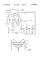
- FIG. 3 a sensing circuit according to the present invention suitable for actuating the previously described sensing method is schematically shown.
- the circuit substantially comprises three digitally-driven variable reference current generators G1, G2, G3 (for example, three digital-to-analog converters with current-mode output) generating three variable reference currents IR1, IR2, IR3, three current comparators 1, 2, 3, three circuits R1, R2, R3 for replicating a current IC sunk by a multiple-level memory cell MC to be sensed, and a sequential machine 4 which controls the three variable reference current generators G1, G2, G3 and provides at its output the n-bit code stored in the memory cell MC.
- G1, G2, G3 for example, three digital-to-analog converters with current-mode output
- IR1, IR2, IR3 three current comparators 1, 2, 3, three circuits R1, R2, R3 for replicating a current IC sunk by a multiple-level memory cell MC to be sensed
- a sequential machine 4
- the current comparator 1 has an inverting input coupled to the drain electrode of the memory cell MC to be sensed through the first current-replicating circuit R1, and a non-inverting input connected to the first variable reference current generator G1.
- An output signal S1 of the current comparator 1 is supplied to the sequential machine 4.
- the current comparator 2 has an inverting input coupled to the drain electrode of the memory cell MC to be sensed through the second current-replicating circuit R2, and a non-inverting input connected to the second variable reference current generator G2.
- An output signal S2 of the current comparator 2 is supplied to the sequential machine 4.
- the current comparator 3 has an inverting input coupled to the drain electrode of the memory cell MC to be sensed through the third current-replicating circuit R3, and a non-inverting input connected to the third variable reference current generator G3. An output signal S3 of the current comparator 3 is supplied to the sequential machine 4.
- the sequential machine 4 is further supplied with a preset signal PR and with a clock signal CK (timing signal), and supplies a group CNT of control signals (in digital format) to the three variable reference current generators G1-G3.
- the sequential machine 4 also generates a group OUT of output signals which, at the end of the sensing procedure, represents the n-bit code stored in the sensed memory cell MC.
- the reference current generator G1 comprises five parallel-connected current generators with the values I3, I0, I4, I8, I12 shown in FIG. 1, each current generator having in series a respective switch controlled by a respective one of five control signals Q0-Q4 forming the group CNT of control signals supplied by the sequential machine 4.
- the reference current generator G2 comprises five parallel-connected current generators with the values I7, I1, I5, I9, I13 shown in FIG. 1, each current generator having in series a respective switch controlled by a respective one of the five control signals Q0-Q4.
- the reference current generator G3 comprises five parallel-connected current generators with the values I11, I2, I6, I10, I14 shown in FIG. 1, each current generator having in series a respective switch controlled by a respective one of the five control signals Q0-Q4. Each one of the five control signals Q0-Q4 controls three switches, one switch for each one of the reference current generators G1-G3.
- Each one of the fifteen current generators comprises one reference memory cell, programmed in one of first fifteen levels ("1"-"15” in FIG. 1) of the sixteen distinct programming levels of the memory cell MC to be sensed, so that when the reference memory cells are biased in the same condition of the memory cells to be read they sink a current of the set IC0-IC14. It appears that with this arrangement the currents generated by the variable reference current generators G1-G3 do not have the values I0-I14 shown in FIG. 1. However, as it will be explained later, it is possible to transform the currents IC0-IC14 sunk by the reference memory cells into the current values I0-I14 by making the current comparators 1-3 unbalanced.
- each one of the fifteen current generators comprises a column of reference memory cells (reference bit line). All the reference memory cells belonging to a reference bit line are programmed at the same programming level.
- the fifteen reference bit lines are grouped together in three groups of five reference bit lines. Each one of the three groups is coupled to a respective current comparator.
- the switches provided in series to each one of the current generators are formed by selection transistors, and correspond to the transistors selecting one of the bit lines of the memory array. In this way, the memory cells in the memory array and the reference memory cells are perfectly similar both from the circuital and from the biasing conditions viewpoints.
- FIG. 5 shows the detailed circuit structure of one of the three current comparators 1-3 of FIG. 3.
- the drain voltages 5 and 6 of DL and DR control the gates of two cross-connected MOSFETs MS1 and MR1 (P-channel type) forming a latch.
- the source electrodes of MS1 and MR1 can be connected to a power supply line VDD through two respective P-channel MOSFETs T3 and T4, which are commonly driven by a signal CKS derived from the clock signal CK (CKS can, for example, be the logic complement of CK).
- the drain electrodes of MS1 and MR1 can be short-circuited to each other by the activation of an N-channel MOSFET TE driven by the signal CKS.
- variable reference current generators G1-G3 are comprised of reference memory cells programmed in one of the first fifteen different programming states "1"-"15" of the memory cells, and since the reference memory cells are biased in the same conditions as the memory cell to be sensed, the current comparators are unbalanced (i.e., the currents IC and IRi to be compared are supplied to the respective input of the different from 1:1, for example, 1 to 0.7).
- This is achieved making the MOSFETs MS1 and MR1 different in size, for example, MS1 with an aspect ratio equal to 0.7 times the aspect ratio of MR1. Thanks to this unbalance, even if the reference memory cells sink currents equal to the memory cell currents IC0-IC14, the reference currents I0-I14 previously listed can be obtained.
- FIG. 6 shows the structure of the sequential machine 4.
- the sequential machine 4 must provide the correct sequence of activation of the switches in the variable reference current generators G1-G3, according to the result of the comparisons of the memory cell current IC with the three reference currents IR1-IR2 in the preceding step of the sensing method.
- the sequential machine 4 comprises a sequential network comprising five flip-flops FF0-FF4 (delay type) implementing the recursive successive approximation search algorithm and activating in the correct sequence the group CNT of control signals Q0-Q4 controlling the switches in the variable reference current generators G1-G3.
- the sequential network keeps memory of the preceding state and, depending on the result of the current comparisons during the current step of the sensing algorithm, determines the future state of the five control signals Q0-Q4.
- Each flip-flop FF0-FF4 has a clock input CK and a preset input PR.
- the clock inputs CK and the preset inputs PR of the flip-flops FF0-FF1 are commonly connected to the clock signal CK and to the preset signal PR, respectively.
- Each flip-flop has a data input D0-D4, a "true” data output Q0-Q4, and a "complemented" data output Q0N-Q4N which is the logic complement of the true data output Q0-Q4.
- the true data output after a clock pulse takes the logic value of the data input during said clock pulse.
- the true data output Q0-Q4 of the flip-flops forms the five control signals of the group CNT controlling the switches in the variable reference current generators G1-G3.
- the data input D0 of FF0 is supplied with the complemented data output Q0N of FF0.
- the data input D1 of FF1 is supplied with the logic NOR of QON and of the output S1 of the first current comparator 1.
- the data input D2 of FF2 is supplied with a logic signal equal to NOT(S2 OR NOT(S1 AND Q0)), where S2 is the output of the second current comparator 2.
- the data input of FF3 is supplied with a logic signal equal to NOT(S3 OR NOT(S2 AND Q0)), where S3 is the output of the third current comparator 3.
- the data input D4 of FF4 is supplied with a logic signal equal to the logic NOR of Q0 and of the logic complement S3N of S3.
- the sequential machine 4 also comprises a combinatorial network, also shown in FIG. 6, which generates the output signals OUT0-OUT3 representing the four-bit code stored in the sensed memory cells.
- the signal OUT0 is equal to NOT(S3N AND NOT(S1 AND S2N)), where S2N is the logic complement of S2.
- the signal OUT1 is equal to S2.
- the signal OUT2 is equal to NOT(Q2 AND Q4N).
- the signal OUT3 is equal to NOT(Q3N AND Q4N).
- the logic state of the output signals OUT0-OUT3 depends on the present state of the sequential machine, i.e., on the present state of the signals Q0-Q4, and on the output signals S1-S3 of the current comparators 1-3 in the last step of the sensing algorithm. Thank to this, the output signals OUT0-OUT3 are already available after one and a half clock cycles, in the first half of the second period of the clock signal CK (FIG. 9).
- FIG. 7 is a truth table of the sequential machine of FIG. 6.
- the sensing of a sixteen-level memory cell MC is carried out in two steps.
- the valid output data OUT0-OUT3 are at t 0 +(3/2 T) (where T is the period of the clock signal CK), i.e., before the end of the second clock pulse.
- T is the period of the clock signal CK
- the sensing method of the present invention represents a better trade-off between the sensing time and the complexity of the sensing circuit with respect to the dichotomic serial sensing method and the parallel sensing method: the time required to sense a memory cell is lower than that required by the dichotomic serial sensing method, and the sensing circuit is less complex (less silicon area) than that required by the parallel sensing method.
Abstract
Description
______________________________________
Programming Level
                Four-Bit Code
______________________________________
IC0 = 0 μA   0000
IC1 = 10 μA  0001
IC2 = 20 μA  0010
IC3 = 30 μA  0011
IC4 = 40 μA  0100
IC5 = 50 μA  0101
IC6 = 60 μA  0110
IC7 = 70 μA  0111
IC8 = 80 μA  1000
IC9 = 90 μA  1001
IC10 = 100 μA
                1010
IC11 = 110 μA
                1011
IC12 = 120 μA
                1100
IC13 = 130 μA
                1101
IC14 = 140 μA
                1110
IC15 = 150 μA
                1111
______________________________________
______________________________________
I0 = 5 μA;
         I1 = 15 μA
                      I2 = 25 μA;
                                 I3 = 35 μA
I4 = 45 μA;
         I5 = 55 μA
                      I6 = 65 μA;
                                 I7 = 75 μA
I8 = 85 μA;
         I9 = 95 μA
                      I10 = 105 μA;
                                 I11 = 115 μA
I12 = 125 μA;
         I13 = 135 μA
                      I14 = 145 μA;
______________________________________
Claims (18)
Applications Claiming Priority (2)
| Application Number | Priority Date | Filing Date | Title |
|---|---|---|---|
| EP95830347A EP0757355B1 (en) | 1995-07-31 | 1995-07-31 | Mixed parallel-dichotomic serial sensing method for sensing multiple-levels non-volatile memory cells, and sensing circuit actuating such method |
| EP95830347 | 1995-07-31 |
Publications (1)
| Publication Number | Publication Date |
|---|---|
| US5729490A true US5729490A (en) | 1998-03-17 |
Family
ID=8221994
Family Applications (1)
| Application Number | Title | Priority Date | Filing Date |
|---|---|---|---|
| US08/690,059 Expired - Lifetime US5729490A (en) | 1995-07-31 | 1996-07-31 | Parallel-dichotomic serial sensing method for sensing multiple-level non-volatile memory cells, and sensing circuit for actuating such method |
Country Status (3)
| Country | Link |
|---|---|
| US (1) | US5729490A (en) |
| EP (1) | EP0757355B1 (en) |
| DE (1) | DE69516402T2 (en) |
Cited By (92)
| Publication number | Priority date | Publication date | Assignee | Title |
|---|---|---|---|---|
| US5909397A (en) * | 1996-10-08 | 1999-06-01 | Texas Instruments Incorporated | Method and system for testing and adjusting threshold voltages in flash eeproms |
| US5930172A (en) * | 1998-06-23 | 1999-07-27 | Advanced Micro Devices, Inc. | Page buffer for a multi-level flash memory with a limited number of latches per memory cell |
| US6005799A (en) * | 1998-08-06 | 1999-12-21 | Silicon Aquarius | Methods and circuits for single-memory dynamic cell multivalue data storage |
| US6084797A (en) * | 1998-03-27 | 2000-07-04 | Stmicroelectronics S.R.L. | Method for reading a multiple-level memory cell |
| US6154390A (en) * | 1999-01-12 | 2000-11-28 | Macronix International Co., Ltd. | Sensing apparatus and method for fetching multi-level cell data |
| US6191977B1 (en) * | 1998-03-28 | 2001-02-20 | Hyundai Electronics Industries Co., Ltd. | Sense circuit for a multi-level flash memory cell |
| US6301149B1 (en) * | 1999-02-26 | 2001-10-09 | Stmicroelectronics S.R.L. | Method for reading a multilevel nonvolatile memory and multilevel nonvolatile memory |
| US6611468B2 (en) * | 2001-01-31 | 2003-08-26 | Mitsubishi Denki Kabushiki Kaisha | Non-volatile semiconductor memory device having sensitive sense amplifier structure |
| US6657895B2 (en) * | 2001-04-10 | 2003-12-02 | Stmicroelectronics S.R.L. | Reading circuit and method for a multilevel non-volatile memory |
| US20040160837A1 (en) * | 2002-12-04 | 2004-08-19 | Stmicroelectronics S.R.L. | Non-volatile memory cell sensing circuit, particularly for low power supply voltages and high capacitive load values |
| US20040228179A1 (en) * | 2003-01-20 | 2004-11-18 | Stmicroelectronics S.R.L. | Parallel sense amplifier with mirroring of the current to be measured into each reference branch |
| US20040233727A1 (en) * | 2003-05-20 | 2004-11-25 | Yasuaki Iwase | Programming verification method of nonvolatile memory cell, semiconductor memory device, and portable electronic apparatus having the semiconductor memory device |
| US20050036368A1 (en) * | 2003-07-21 | 2005-02-17 | Yeh Chih Chieh | Method for programming programmable eraseless memory |
| US20050035429A1 (en) * | 2003-08-15 | 2005-02-17 | Yeh Chih Chieh | Programmable eraseless memory |
| US20050037546A1 (en) * | 2003-07-21 | 2005-02-17 | Yeh Chih Chieh | Method for manufacturing a programmable eraseless memory |
| US20050063236A1 (en) * | 2003-08-06 | 2005-03-24 | Stmicroelectronics S.R.I | Sense amplifier |
| US20060017598A1 (en) * | 2004-05-18 | 2006-01-26 | Slicex, Inc. | Current mode analog-to-digital converter |
| US20060140010A1 (en) * | 2004-12-29 | 2006-06-29 | Lorenzo Bedarida | Method and system for reducing soft-writing in a multi-level flash memory |
| US20100058146A1 (en) * | 2007-12-12 | 2010-03-04 | Hanan Weingarten | Chien-search system employing a clock-gating scheme to save power for error correction decoder and other applications |
| US20100131580A1 (en) * | 2008-03-25 | 2010-05-27 | Densbits Technologies Ltd. | Apparatus and methods for hardware-efficient unbiased rounding |
| US20100131831A1 (en) * | 2007-12-05 | 2010-05-27 | Hanan Weingarten | low power chien-search based bch/rs decoding system for flash memory, mobile communications devices and other applications |
| US20100146191A1 (en) * | 2007-12-05 | 2010-06-10 | Michael Katz | System and methods employing mock thresholds to generate actual reading thresholds in flash memory devices |
| US20100199149A1 (en) * | 2007-12-05 | 2010-08-05 | Hanan Weingarten | Flash memory apparatus and methods using a plurality of decoding stages including optional use of concatenated bch codes and/or designation of "first below" cells |
| US20100211724A1 (en) * | 2007-09-20 | 2010-08-19 | Hanan Weingarten | Systems and methods for determining logical values of coupled flash memory cells |
| US20100253555A1 (en) * | 2009-04-06 | 2010-10-07 | Hanan Weingarten | Encoding method and system, decoding method and system |
| US20110022886A1 (en) * | 2009-07-22 | 2011-01-27 | Silicon Motion, Inc. | Data storage device and data read method |
| US20110051521A1 (en) * | 2009-08-26 | 2011-03-03 | Shmuel Levy | Flash memory module and method for programming a page of flash memory cells |
| US20110119562A1 (en) * | 2009-11-19 | 2011-05-19 | Steiner Avi | System and method for uncoded bit error rate equalization via interleaving |
| US20110153919A1 (en) * | 2009-12-22 | 2011-06-23 | Erez Sabbag | Device, system, and method for reducing program/read disturb in flash arrays |
| US20110161775A1 (en) * | 2009-12-24 | 2011-06-30 | Hanan Weingarten | System and method for setting a flash memory cell read threshold |
| US20110214029A1 (en) * | 2010-02-28 | 2011-09-01 | Steiner Avi | System and method for multi-dimensional decoding |
| US8327246B2 (en) | 2007-12-18 | 2012-12-04 | Densbits Technologies Ltd. | Apparatus for coding at a plurality of rates in multi-level flash memory systems, and methods useful in conjunction therewith |
| US8332725B2 (en) | 2008-08-20 | 2012-12-11 | Densbits Technologies Ltd. | Reprogramming non volatile memory portions |
| US8359516B2 (en) | 2007-12-12 | 2013-01-22 | Densbits Technologies Ltd. | Systems and methods for error correction and decoding on multi-level physical media |
| US8365040B2 (en) | 2007-09-20 | 2013-01-29 | Densbits Technologies Ltd. | Systems and methods for handling immediate data errors in flash memory |
| US8443242B2 (en) | 2007-10-25 | 2013-05-14 | Densbits Technologies Ltd. | Systems and methods for multiple coding rates in flash devices |
| US8468431B2 (en) | 2010-07-01 | 2013-06-18 | Densbits Technologies Ltd. | System and method for multi-dimensional encoding and decoding |
| US8467249B2 (en) | 2010-07-06 | 2013-06-18 | Densbits Technologies Ltd. | Systems and methods for storing, retrieving, and adjusting read thresholds in flash memory storage system |
| US8508995B2 (en) | 2010-09-15 | 2013-08-13 | Densbits Technologies Ltd. | System and method for adjusting read voltage thresholds in memories |
| US8516274B2 (en) | 2010-04-06 | 2013-08-20 | Densbits Technologies Ltd. | Method, system and medium for analog encryption in a flash memory |
| US8527840B2 (en) | 2010-04-06 | 2013-09-03 | Densbits Technologies Ltd. | System and method for restoring damaged data programmed on a flash device |
| US8539311B2 (en) | 2010-07-01 | 2013-09-17 | Densbits Technologies Ltd. | System and method for data recovery in multi-level cell memories |
| US8553468B2 (en) | 2011-09-21 | 2013-10-08 | Densbits Technologies Ltd. | System and method for managing erase operations in a non-volatile memory |
| US8566510B2 (en) | 2009-05-12 | 2013-10-22 | Densbits Technologies Ltd. | Systems and method for flash memory management |
| US8588003B1 (en) | 2011-08-01 | 2013-11-19 | Densbits Technologies Ltd. | System, method and computer program product for programming and for recovering from a power failure |
| US8667211B2 (en) | 2011-06-01 | 2014-03-04 | Densbits Technologies Ltd. | System and method for managing a non-volatile memory |
| US8694715B2 (en) | 2007-10-22 | 2014-04-08 | Densbits Technologies Ltd. | Methods for adaptively programming flash memory devices and flash memory systems incorporating same |
| US8693258B2 (en) | 2011-03-17 | 2014-04-08 | Densbits Technologies Ltd. | Obtaining soft information using a hard interface |
| US8724387B2 (en) | 2009-10-22 | 2014-05-13 | Densbits Technologies Ltd. | Method, system, and computer readable medium for reading and programming flash memory cells using multiple bias voltages |
| US8730729B2 (en) | 2009-10-15 | 2014-05-20 | Densbits Technologies Ltd. | Systems and methods for averaging error rates in non-volatile devices and storage systems |
| US8745317B2 (en) | 2010-04-07 | 2014-06-03 | Densbits Technologies Ltd. | System and method for storing information in a multi-level cell memory |
| US8819385B2 (en) | 2009-04-06 | 2014-08-26 | Densbits Technologies Ltd. | Device and method for managing a flash memory |
| US8838937B1 (en) | 2012-05-23 | 2014-09-16 | Densbits Technologies Ltd. | Methods, systems and computer readable medium for writing and reading data |
| US8850100B2 (en) | 2010-12-07 | 2014-09-30 | Densbits Technologies Ltd. | Interleaving codeword portions between multiple planes and/or dies of a flash memory device |
| US8868821B2 (en) | 2009-08-26 | 2014-10-21 | Densbits Technologies Ltd. | Systems and methods for pre-equalization and code design for a flash memory |
| US8879325B1 (en) | 2012-05-30 | 2014-11-04 | Densbits Technologies Ltd. | System, method and computer program product for processing read threshold information and for reading a flash memory module |
| US8947941B2 (en) | 2012-02-09 | 2015-02-03 | Densbits Technologies Ltd. | State responsive operations relating to flash memory cells |
| US8964464B2 (en) | 2010-08-24 | 2015-02-24 | Densbits Technologies Ltd. | System and method for accelerated sampling |
| US8990665B1 (en) | 2011-04-06 | 2015-03-24 | Densbits Technologies Ltd. | System, method and computer program product for joint search of a read threshold and soft decoding |
| US8996788B2 (en) | 2012-02-09 | 2015-03-31 | Densbits Technologies Ltd. | Configurable flash interface |
| US8995197B1 (en) | 2009-08-26 | 2015-03-31 | Densbits Technologies Ltd. | System and methods for dynamic erase and program control for flash memory device memories |
| US8996793B1 (en) | 2012-04-24 | 2015-03-31 | Densbits Technologies Ltd. | System, method and computer readable medium for generating soft information |
| US8996790B1 (en) | 2011-05-12 | 2015-03-31 | Densbits Technologies Ltd. | System and method for flash memory management |
| US9021177B2 (en) | 2010-04-29 | 2015-04-28 | Densbits Technologies Ltd. | System and method for allocating and using spare blocks in a flash memory |
| US9063878B2 (en) | 2010-11-03 | 2015-06-23 | Densbits Technologies Ltd. | Method, system and computer readable medium for copy back |
| US9069659B1 (en) | 2013-01-03 | 2015-06-30 | Densbits Technologies Ltd. | Read threshold determination using reference read threshold |
| US9110785B1 (en) | 2011-05-12 | 2015-08-18 | Densbits Technologies Ltd. | Ordered merge of data sectors that belong to memory space portions |
| US9136876B1 (en) | 2013-06-13 | 2015-09-15 | Densbits Technologies Ltd. | Size limited multi-dimensional decoding |
| US9195592B1 (en) | 2011-05-12 | 2015-11-24 | Densbits Technologies Ltd. | Advanced management of a non-volatile memory |
| US9330767B1 (en) | 2009-08-26 | 2016-05-03 | Avago Technologies General Ip (Singapore) Pte. Ltd. | Flash memory module and method for programming a page of flash memory cells |
| US9348694B1 (en) | 2013-10-09 | 2016-05-24 | Avago Technologies General Ip (Singapore) Pte. Ltd. | Detecting and managing bad columns |
| US9368225B1 (en) | 2012-11-21 | 2016-06-14 | Avago Technologies General Ip (Singapore) Pte. Ltd. | Determining read thresholds based upon read error direction statistics |
| US9372792B1 (en) | 2011-05-12 | 2016-06-21 | Avago Technologies General Ip (Singapore) Pte. Ltd. | Advanced management of a non-volatile memory |
| US9397706B1 (en) | 2013-10-09 | 2016-07-19 | Avago Technologies General Ip (Singapore) Pte. Ltd. | System and method for irregular multiple dimension decoding and encoding |
| US9396106B2 (en) | 2011-05-12 | 2016-07-19 | Avago Technologies General Ip (Singapore) Pte. Ltd. | Advanced management of a non-volatile memory |
| US9407291B1 (en) | 2014-07-03 | 2016-08-02 | Avago Technologies General Ip (Singapore) Pte. Ltd. | Parallel encoding method and system |
| US9413491B1 (en) | 2013-10-08 | 2016-08-09 | Avago Technologies General Ip (Singapore) Pte. Ltd. | System and method for multiple dimension decoding and encoding a message |
| US9449702B1 (en) | 2014-07-08 | 2016-09-20 | Avago Technologies General Ip (Singapore) Pte. Ltd. | Power management |
| US9501392B1 (en) | 2011-05-12 | 2016-11-22 | Avago Technologies General Ip (Singapore) Pte. Ltd. | Management of a non-volatile memory module |
| US9524211B1 (en) | 2014-11-18 | 2016-12-20 | Avago Technologies General Ip (Singapore) Pte. Ltd. | Codeword management |
| US9536612B1 (en) | 2014-01-23 | 2017-01-03 | Avago Technologies General Ip (Singapore) Pte. Ltd | Digital signaling processing for three dimensional flash memory arrays |
| US9542262B1 (en) | 2014-05-29 | 2017-01-10 | Avago Technologies General Ip (Singapore) Pte. Ltd. | Error correction |
| US9786388B1 (en) | 2013-10-09 | 2017-10-10 | Avago Technologies General Ip (Singapore) Pte. Ltd. | Detecting and managing bad columns |
| US9851921B1 (en) | 2015-07-05 | 2017-12-26 | Avago Technologies General Ip (Singapore) Pte. Ltd. | Flash memory chip processing |
| US9892033B1 (en) | 2014-06-24 | 2018-02-13 | Avago Technologies General Ip (Singapore) Pte. Ltd. | Management of memory units |
| US9921954B1 (en) | 2012-08-27 | 2018-03-20 | Avago Technologies General Ip (Singapore) Pte. Ltd. | Method and system for split flash memory management between host and storage controller |
| US9954558B1 (en) | 2016-03-03 | 2018-04-24 | Avago Technologies General Ip (Singapore) Pte. Ltd. | Fast decoding of data stored in a flash memory |
| US9972393B1 (en) | 2014-07-03 | 2018-05-15 | Avago Technologies General Ip (Singapore) Pte. Ltd. | Accelerating programming of a flash memory module |
| US10079068B2 (en) | 2011-02-23 | 2018-09-18 | Avago Technologies General Ip (Singapore) Pte. Ltd. | Devices and method for wear estimation based memory management |
| US10120792B1 (en) | 2014-01-29 | 2018-11-06 | Avago Technologies General Ip (Singapore) Pte. Ltd. | Programming an embedded flash storage device |
| US10305515B1 (en) | 2015-02-02 | 2019-05-28 | Avago Technologies International Sales Pte. Limited | System and method for encoding using multiple linear feedback shift registers |
| US10628255B1 (en) | 2015-06-11 | 2020-04-21 | Avago Technologies International Sales Pte. Limited | Multi-dimensional decoding |
Families Citing this family (2)
| Publication number | Priority date | Publication date | Assignee | Title |
|---|---|---|---|---|
| EP1211812B1 (en) | 2000-10-31 | 2006-11-15 | STMicroelectronics S.r.l. | A/D conversion method in high density multilevel non-volatile memory devices and corresponding converter device |
| US6912150B2 (en) * | 2003-05-13 | 2005-06-28 | Lionel Portman | Reference current generator, and method of programming, adjusting and/or operating same |
Citations (10)
| Publication number | Priority date | Publication date | Assignee | Title |
|---|---|---|---|---|
| EP0057111A2 (en) * | 1981-01-28 | 1982-08-04 | General Instrument Corporation | Read only memory |
| US4544917A (en) * | 1982-09-16 | 1985-10-01 | Westinghouse Electric Corp. | A/D converter having digitally controlled subranging and self-alignment apparatus for use therein |
| US4749984A (en) * | 1987-06-29 | 1988-06-07 | Rca Corporation | Subranging A/D converter with converging digitally controlled voltages |
| US4964079A (en) * | 1988-04-26 | 1990-10-16 | Sgs-Thomson Microelectronics | Electrically programmable memory with several information bits per cell |
| US5019820A (en) * | 1988-08-29 | 1991-05-28 | Matsushita Electric Industrial Co., Ltd. | Serial-parallel type A/D converter having reference resistor chain and current source array |
| US5070332A (en) * | 1991-03-18 | 1991-12-03 | Burr-Brown Corporation | Two-step subranging analog to digital converter |
| US5142495A (en) * | 1989-03-10 | 1992-08-25 | Intel Corporation | Variable load for margin mode |
| US5163021A (en) * | 1989-04-13 | 1992-11-10 | Sundisk Corporation | Multi-state EEprom read and write circuits and techniques |
| US5381374A (en) * | 1992-01-09 | 1995-01-10 | Kabushiki Kaisha Toshiba | Memory cell data output circuit having improved access time |
| US5638322A (en) * | 1995-07-19 | 1997-06-10 | Cypress Semiconductor Corp. | Apparatus and method for improving common mode noise rejection in pseudo-differential sense amplifiers |
-
1995
- 1995-07-31 EP EP95830347A patent/EP0757355B1/en not_active Expired - Lifetime
- 1995-07-31 DE DE69516402T patent/DE69516402T2/en not_active Expired - Lifetime
-
1996
- 1996-07-31 US US08/690,059 patent/US5729490A/en not_active Expired - Lifetime
Patent Citations (10)
| Publication number | Priority date | Publication date | Assignee | Title |
|---|---|---|---|---|
| EP0057111A2 (en) * | 1981-01-28 | 1982-08-04 | General Instrument Corporation | Read only memory |
| US4544917A (en) * | 1982-09-16 | 1985-10-01 | Westinghouse Electric Corp. | A/D converter having digitally controlled subranging and self-alignment apparatus for use therein |
| US4749984A (en) * | 1987-06-29 | 1988-06-07 | Rca Corporation | Subranging A/D converter with converging digitally controlled voltages |
| US4964079A (en) * | 1988-04-26 | 1990-10-16 | Sgs-Thomson Microelectronics | Electrically programmable memory with several information bits per cell |
| US5019820A (en) * | 1988-08-29 | 1991-05-28 | Matsushita Electric Industrial Co., Ltd. | Serial-parallel type A/D converter having reference resistor chain and current source array |
| US5142495A (en) * | 1989-03-10 | 1992-08-25 | Intel Corporation | Variable load for margin mode |
| US5163021A (en) * | 1989-04-13 | 1992-11-10 | Sundisk Corporation | Multi-state EEprom read and write circuits and techniques |
| US5070332A (en) * | 1991-03-18 | 1991-12-03 | Burr-Brown Corporation | Two-step subranging analog to digital converter |
| US5381374A (en) * | 1992-01-09 | 1995-01-10 | Kabushiki Kaisha Toshiba | Memory cell data output circuit having improved access time |
| US5638322A (en) * | 1995-07-19 | 1997-06-10 | Cypress Semiconductor Corp. | Apparatus and method for improving common mode noise rejection in pseudo-differential sense amplifiers |
Non-Patent Citations (6)
| Title |
|---|
| Bauer, M., et al., "A Multilevel Cell 32MB Flash Memory," IEEE International Solid-State Circuits Conference, Feb. 16, 1995, pp. 119, 132-133, 351. |
| Bauer, M., et al., A Multilevel Cell 32MB Flash Memory , IEEE International Solid State Circuits Conference, Feb. 16, 1995, pp. 119, 132 133, 351. * |
| Bleiker, Christoph et al., "A Four-State EEPROM Using Floating-Gate Memory Cells," IEEE Journal of Solid-State Circuits, vol. SC-22, No. 3, Jun. 1987, pp. 460-463. |
| Bleiker, Christoph et al., A Four State EEPROM Using Floating Gate Memory Cells , IEEE Journal of Solid State Circuits, vol. SC 22, No. 3, Jun. 1987, pp. 460 463. * |
| Horiguchi, Masashi et al, "An Experimental Large-Capacity Semiconductor File Memory Using 16-Levels/Cell Storage," IEEE Journal of Solid-State Circuits, vol. 23, No. 1, Feb. 1988, pp. 27-32. |
| Horiguchi, Masashi et al, An Experimental Large Capacity Semiconductor File Memory Using 16 Levels/Cell Storage , IEEE Journal of Solid State Circuits, vol. 23, No. 1, Feb. 1988, pp. 27 32. * |
Cited By (135)
| Publication number | Priority date | Publication date | Assignee | Title |
|---|---|---|---|---|
| US5909397A (en) * | 1996-10-08 | 1999-06-01 | Texas Instruments Incorporated | Method and system for testing and adjusting threshold voltages in flash eeproms |
| US6084797A (en) * | 1998-03-27 | 2000-07-04 | Stmicroelectronics S.R.L. | Method for reading a multiple-level memory cell |
| US6191977B1 (en) * | 1998-03-28 | 2001-02-20 | Hyundai Electronics Industries Co., Ltd. | Sense circuit for a multi-level flash memory cell |
| US5930172A (en) * | 1998-06-23 | 1999-07-27 | Advanced Micro Devices, Inc. | Page buffer for a multi-level flash memory with a limited number of latches per memory cell |
| US6005799A (en) * | 1998-08-06 | 1999-12-21 | Silicon Aquarius | Methods and circuits for single-memory dynamic cell multivalue data storage |
| US6154390A (en) * | 1999-01-12 | 2000-11-28 | Macronix International Co., Ltd. | Sensing apparatus and method for fetching multi-level cell data |
| US6178114B1 (en) * | 1999-01-12 | 2001-01-23 | Macronix International Co., Ltd. | Sensing apparatus and method for fetching multi-level cell data |
| US6301149B1 (en) * | 1999-02-26 | 2001-10-09 | Stmicroelectronics S.R.L. | Method for reading a multilevel nonvolatile memory and multilevel nonvolatile memory |
| US6611468B2 (en) * | 2001-01-31 | 2003-08-26 | Mitsubishi Denki Kabushiki Kaisha | Non-volatile semiconductor memory device having sensitive sense amplifier structure |
| US6657895B2 (en) * | 2001-04-10 | 2003-12-02 | Stmicroelectronics S.R.L. | Reading circuit and method for a multilevel non-volatile memory |
| US20040160837A1 (en) * | 2002-12-04 | 2004-08-19 | Stmicroelectronics S.R.L. | Non-volatile memory cell sensing circuit, particularly for low power supply voltages and high capacitive load values |
| US6894934B2 (en) * | 2002-12-04 | 2005-05-17 | Stmicroelectronics S.R.L. | Non-volatile memory cell sensing circuit, particularly for low power supply voltages and high capacitive load values |
| US20040228179A1 (en) * | 2003-01-20 | 2004-11-18 | Stmicroelectronics S.R.L. | Parallel sense amplifier with mirroring of the current to be measured into each reference branch |
| US7075844B2 (en) * | 2003-01-20 | 2006-07-11 | Stmicroelectronics S.R.L. | Parallel sense amplifier with mirroring of the current to be measured into each reference branch |
| US20040233727A1 (en) * | 2003-05-20 | 2004-11-25 | Yasuaki Iwase | Programming verification method of nonvolatile memory cell, semiconductor memory device, and portable electronic apparatus having the semiconductor memory device |
| US6992933B2 (en) * | 2003-05-20 | 2006-01-31 | Sharp Kabushiki Kaisha | Programming verification method of nonvolatile memory cell, semiconductor memory device, and portable electronic apparatus having the semiconductor memory device |
| US7132350B2 (en) | 2003-07-21 | 2006-11-07 | Macronix International Co., Ltd. | Method for manufacturing a programmable eraseless memory |
| US20050036368A1 (en) * | 2003-07-21 | 2005-02-17 | Yeh Chih Chieh | Method for programming programmable eraseless memory |
| US20050190601A1 (en) * | 2003-07-21 | 2005-09-01 | Macronix International Co. Ltd | Programmable resistor eraseless memory |
| US20050037546A1 (en) * | 2003-07-21 | 2005-02-17 | Yeh Chih Chieh | Method for manufacturing a programmable eraseless memory |
| US8501591B2 (en) | 2003-07-21 | 2013-08-06 | Macronix International Co., Ltd. | Method for manufacturing a multiple-bit-per-cell memory |
| US7180123B2 (en) | 2003-07-21 | 2007-02-20 | Macronix International Co., Ltd. | Method for programming programmable eraseless memory |
| US20050063236A1 (en) * | 2003-08-06 | 2005-03-24 | Stmicroelectronics S.R.I | Sense amplifier |
| US7136305B2 (en) * | 2003-08-06 | 2006-11-14 | Stmicroelectronics S.R.L. | Sense amplifier with equalizer |
| US20050035429A1 (en) * | 2003-08-15 | 2005-02-17 | Yeh Chih Chieh | Programmable eraseless memory |
| US20060017598A1 (en) * | 2004-05-18 | 2006-01-26 | Slicex, Inc. | Current mode analog-to-digital converter |
| US7081845B2 (en) * | 2004-05-18 | 2006-07-25 | Slicex, Inc. | Current mode analog-to-digital converter |
| US20060140010A1 (en) * | 2004-12-29 | 2006-06-29 | Lorenzo Bedarida | Method and system for reducing soft-writing in a multi-level flash memory |
| US7522455B2 (en) | 2004-12-29 | 2009-04-21 | Atmel Corporation | Method and system for reducing soft-writing in a multi-level flash memory |
| US8650352B2 (en) | 2007-09-20 | 2014-02-11 | Densbits Technologies Ltd. | Systems and methods for determining logical values of coupled flash memory cells |
| US8365040B2 (en) | 2007-09-20 | 2013-01-29 | Densbits Technologies Ltd. | Systems and methods for handling immediate data errors in flash memory |
| US20100211724A1 (en) * | 2007-09-20 | 2010-08-19 | Hanan Weingarten | Systems and methods for determining logical values of coupled flash memory cells |
| US8799563B2 (en) | 2007-10-22 | 2014-08-05 | Densbits Technologies Ltd. | Methods for adaptively programming flash memory devices and flash memory systems incorporating same |
| US8694715B2 (en) | 2007-10-22 | 2014-04-08 | Densbits Technologies Ltd. | Methods for adaptively programming flash memory devices and flash memory systems incorporating same |
| US8443242B2 (en) | 2007-10-25 | 2013-05-14 | Densbits Technologies Ltd. | Systems and methods for multiple coding rates in flash devices |
| US8627188B2 (en) | 2007-12-05 | 2014-01-07 | Densbits Technologies Ltd. | Flash memory apparatus and methods using a plurality of decoding stages including optional use of concatenated BCH codes and/or designation of “first below” cells |
| US20100180073A1 (en) * | 2007-12-05 | 2010-07-15 | Hanan Weingarten | Flash memory device with physical cell value deterioration accommodation and methods useful in conjunction therewith |
| US8843698B2 (en) | 2007-12-05 | 2014-09-23 | Densbits Technologies Ltd. | Systems and methods for temporarily retiring memory portions |
| US9104550B2 (en) | 2007-12-05 | 2015-08-11 | Densbits Technologies Ltd. | Physical levels deterioration based determination of thresholds useful for converting cell physical levels into cell logical values in an array of digital memory cells |
| US8453022B2 (en) | 2007-12-05 | 2013-05-28 | Densbits Technologies Ltd. | Apparatus and methods for generating row-specific reading thresholds in flash memory |
| US20100199149A1 (en) * | 2007-12-05 | 2010-08-05 | Hanan Weingarten | Flash memory apparatus and methods using a plurality of decoding stages including optional use of concatenated bch codes and/or designation of "first below" cells |
| US8751726B2 (en) | 2007-12-05 | 2014-06-10 | Densbits Technologies Ltd. | System and methods employing mock thresholds to generate actual reading thresholds in flash memory devices |
| US20100131831A1 (en) * | 2007-12-05 | 2010-05-27 | Hanan Weingarten | low power chien-search based bch/rs decoding system for flash memory, mobile communications devices and other applications |
| US20100146191A1 (en) * | 2007-12-05 | 2010-06-10 | Michael Katz | System and methods employing mock thresholds to generate actual reading thresholds in flash memory devices |
| US8341335B2 (en) | 2007-12-05 | 2012-12-25 | Densbits Technologies Ltd. | Flash memory apparatus with a heating system for temporarily retired memory portions |
| US8607128B2 (en) | 2007-12-05 | 2013-12-10 | Densbits Technologies Ltd. | Low power chien-search based BCH/RS decoding system for flash memory, mobile communications devices and other applications |
| US8321625B2 (en) | 2007-12-05 | 2012-11-27 | Densbits Technologies Ltd. | Flash memory device with physical cell value deterioration accommodation and methods useful in conjunction therewith |
| US8335977B2 (en) | 2007-12-05 | 2012-12-18 | Densbits Technologies Ltd. | Flash memory apparatus and methods using a plurality of decoding stages including optional use of concatenated BCH codes and/or designation of “first below” cells |
| US8782500B2 (en) | 2007-12-12 | 2014-07-15 | Densbits Technologies Ltd. | Systems and methods for error correction and decoding on multi-level physical media |
| US8276051B2 (en) | 2007-12-12 | 2012-09-25 | Densbits Technologies Ltd. | Chien-search system employing a clock-gating scheme to save power for error correction decoder and other applications |
| US20100058146A1 (en) * | 2007-12-12 | 2010-03-04 | Hanan Weingarten | Chien-search system employing a clock-gating scheme to save power for error correction decoder and other applications |
| US8359516B2 (en) | 2007-12-12 | 2013-01-22 | Densbits Technologies Ltd. | Systems and methods for error correction and decoding on multi-level physical media |
| US8327246B2 (en) | 2007-12-18 | 2012-12-04 | Densbits Technologies Ltd. | Apparatus for coding at a plurality of rates in multi-level flash memory systems, and methods useful in conjunction therewith |
| US8762800B1 (en) | 2008-01-31 | 2014-06-24 | Densbits Technologies Ltd. | Systems and methods for handling immediate data errors in flash memory |
| US8972472B2 (en) | 2008-03-25 | 2015-03-03 | Densbits Technologies Ltd. | Apparatus and methods for hardware-efficient unbiased rounding |
| US20100131580A1 (en) * | 2008-03-25 | 2010-05-27 | Densbits Technologies Ltd. | Apparatus and methods for hardware-efficient unbiased rounding |
| US8332725B2 (en) | 2008-08-20 | 2012-12-11 | Densbits Technologies Ltd. | Reprogramming non volatile memory portions |
| US8458574B2 (en) | 2009-04-06 | 2013-06-04 | Densbits Technologies Ltd. | Compact chien-search based decoding apparatus and method |
| US8850296B2 (en) | 2009-04-06 | 2014-09-30 | Densbits Technologies Ltd. | Encoding method and system, decoding method and system |
| US20100253555A1 (en) * | 2009-04-06 | 2010-10-07 | Hanan Weingarten | Encoding method and system, decoding method and system |
| US8819385B2 (en) | 2009-04-06 | 2014-08-26 | Densbits Technologies Ltd. | Device and method for managing a flash memory |
| US8566510B2 (en) | 2009-05-12 | 2013-10-22 | Densbits Technologies Ltd. | Systems and method for flash memory management |
| US20110022886A1 (en) * | 2009-07-22 | 2011-01-27 | Silicon Motion, Inc. | Data storage device and data read method |
| US8120965B2 (en) * | 2009-07-22 | 2012-02-21 | Silicon Motion, Inc. | Data storage device and data read method |
| US20110051521A1 (en) * | 2009-08-26 | 2011-03-03 | Shmuel Levy | Flash memory module and method for programming a page of flash memory cells |
| US9330767B1 (en) | 2009-08-26 | 2016-05-03 | Avago Technologies General Ip (Singapore) Pte. Ltd. | Flash memory module and method for programming a page of flash memory cells |
| US8868821B2 (en) | 2009-08-26 | 2014-10-21 | Densbits Technologies Ltd. | Systems and methods for pre-equalization and code design for a flash memory |
| US8305812B2 (en) | 2009-08-26 | 2012-11-06 | Densbits Technologies Ltd. | Flash memory module and method for programming a page of flash memory cells |
| US8995197B1 (en) | 2009-08-26 | 2015-03-31 | Densbits Technologies Ltd. | System and methods for dynamic erase and program control for flash memory device memories |
| US8730729B2 (en) | 2009-10-15 | 2014-05-20 | Densbits Technologies Ltd. | Systems and methods for averaging error rates in non-volatile devices and storage systems |
| US8724387B2 (en) | 2009-10-22 | 2014-05-13 | Densbits Technologies Ltd. | Method, system, and computer readable medium for reading and programming flash memory cells using multiple bias voltages |
| US20110119562A1 (en) * | 2009-11-19 | 2011-05-19 | Steiner Avi | System and method for uncoded bit error rate equalization via interleaving |
| US8626988B2 (en) | 2009-11-19 | 2014-01-07 | Densbits Technologies Ltd. | System and method for uncoded bit error rate equalization via interleaving |
| US20110153919A1 (en) * | 2009-12-22 | 2011-06-23 | Erez Sabbag | Device, system, and method for reducing program/read disturb in flash arrays |
| US9037777B2 (en) | 2009-12-22 | 2015-05-19 | Densbits Technologies Ltd. | Device, system, and method for reducing program/read disturb in flash arrays |
| US8607124B2 (en) | 2009-12-24 | 2013-12-10 | Densbits Technologies Ltd. | System and method for setting a flash memory cell read threshold |
| US20110161775A1 (en) * | 2009-12-24 | 2011-06-30 | Hanan Weingarten | System and method for setting a flash memory cell read threshold |
| US8341502B2 (en) | 2010-02-28 | 2012-12-25 | Densbits Technologies Ltd. | System and method for multi-dimensional decoding |
| US8700970B2 (en) | 2010-02-28 | 2014-04-15 | Densbits Technologies Ltd. | System and method for multi-dimensional decoding |
| US20110214039A1 (en) * | 2010-02-28 | 2011-09-01 | Steiner Avi | System and method for multi-dimensional decoding |
| US20110214029A1 (en) * | 2010-02-28 | 2011-09-01 | Steiner Avi | System and method for multi-dimensional decoding |
| US9104610B2 (en) | 2010-04-06 | 2015-08-11 | Densbits Technologies Ltd. | Method, system and medium for analog encryption in a flash memory |
| US8527840B2 (en) | 2010-04-06 | 2013-09-03 | Densbits Technologies Ltd. | System and method for restoring damaged data programmed on a flash device |
| US8516274B2 (en) | 2010-04-06 | 2013-08-20 | Densbits Technologies Ltd. | Method, system and medium for analog encryption in a flash memory |
| US8745317B2 (en) | 2010-04-07 | 2014-06-03 | Densbits Technologies Ltd. | System and method for storing information in a multi-level cell memory |
| US9021177B2 (en) | 2010-04-29 | 2015-04-28 | Densbits Technologies Ltd. | System and method for allocating and using spare blocks in a flash memory |
| US8850297B1 (en) | 2010-07-01 | 2014-09-30 | Densbits Technologies Ltd. | System and method for multi-dimensional encoding and decoding |
| US8468431B2 (en) | 2010-07-01 | 2013-06-18 | Densbits Technologies Ltd. | System and method for multi-dimensional encoding and decoding |
| US8510639B2 (en) | 2010-07-01 | 2013-08-13 | Densbits Technologies Ltd. | System and method for multi-dimensional encoding and decoding |
| US8539311B2 (en) | 2010-07-01 | 2013-09-17 | Densbits Technologies Ltd. | System and method for data recovery in multi-level cell memories |
| US8621321B2 (en) | 2010-07-01 | 2013-12-31 | Densbits Technologies Ltd. | System and method for multi-dimensional encoding and decoding |
| US8467249B2 (en) | 2010-07-06 | 2013-06-18 | Densbits Technologies Ltd. | Systems and methods for storing, retrieving, and adjusting read thresholds in flash memory storage system |
| US8964464B2 (en) | 2010-08-24 | 2015-02-24 | Densbits Technologies Ltd. | System and method for accelerated sampling |
| US8508995B2 (en) | 2010-09-15 | 2013-08-13 | Densbits Technologies Ltd. | System and method for adjusting read voltage thresholds in memories |
| US9063878B2 (en) | 2010-11-03 | 2015-06-23 | Densbits Technologies Ltd. | Method, system and computer readable medium for copy back |
| US8850100B2 (en) | 2010-12-07 | 2014-09-30 | Densbits Technologies Ltd. | Interleaving codeword portions between multiple planes and/or dies of a flash memory device |
| US10079068B2 (en) | 2011-02-23 | 2018-09-18 | Avago Technologies General Ip (Singapore) Pte. Ltd. | Devices and method for wear estimation based memory management |
| US8693258B2 (en) | 2011-03-17 | 2014-04-08 | Densbits Technologies Ltd. | Obtaining soft information using a hard interface |
| US8990665B1 (en) | 2011-04-06 | 2015-03-24 | Densbits Technologies Ltd. | System, method and computer program product for joint search of a read threshold and soft decoding |
| US8996790B1 (en) | 2011-05-12 | 2015-03-31 | Densbits Technologies Ltd. | System and method for flash memory management |
| US9372792B1 (en) | 2011-05-12 | 2016-06-21 | Avago Technologies General Ip (Singapore) Pte. Ltd. | Advanced management of a non-volatile memory |
| US9501392B1 (en) | 2011-05-12 | 2016-11-22 | Avago Technologies General Ip (Singapore) Pte. Ltd. | Management of a non-volatile memory module |
| US9110785B1 (en) | 2011-05-12 | 2015-08-18 | Densbits Technologies Ltd. | Ordered merge of data sectors that belong to memory space portions |
| US9195592B1 (en) | 2011-05-12 | 2015-11-24 | Densbits Technologies Ltd. | Advanced management of a non-volatile memory |
| US9396106B2 (en) | 2011-05-12 | 2016-07-19 | Avago Technologies General Ip (Singapore) Pte. Ltd. | Advanced management of a non-volatile memory |
| US8667211B2 (en) | 2011-06-01 | 2014-03-04 | Densbits Technologies Ltd. | System and method for managing a non-volatile memory |
| US8588003B1 (en) | 2011-08-01 | 2013-11-19 | Densbits Technologies Ltd. | System, method and computer program product for programming and for recovering from a power failure |
| US8553468B2 (en) | 2011-09-21 | 2013-10-08 | Densbits Technologies Ltd. | System and method for managing erase operations in a non-volatile memory |
| US8996788B2 (en) | 2012-02-09 | 2015-03-31 | Densbits Technologies Ltd. | Configurable flash interface |
| US8947941B2 (en) | 2012-02-09 | 2015-02-03 | Densbits Technologies Ltd. | State responsive operations relating to flash memory cells |
| US8996793B1 (en) | 2012-04-24 | 2015-03-31 | Densbits Technologies Ltd. | System, method and computer readable medium for generating soft information |
| US8838937B1 (en) | 2012-05-23 | 2014-09-16 | Densbits Technologies Ltd. | Methods, systems and computer readable medium for writing and reading data |
| US9431118B1 (en) | 2012-05-30 | 2016-08-30 | Avago Technologies General Ip (Singapore) Pte. Ltd. | System, method and computer program product for processing read threshold information and for reading a flash memory module |
| US8879325B1 (en) | 2012-05-30 | 2014-11-04 | Densbits Technologies Ltd. | System, method and computer program product for processing read threshold information and for reading a flash memory module |
| US9921954B1 (en) | 2012-08-27 | 2018-03-20 | Avago Technologies General Ip (Singapore) Pte. Ltd. | Method and system for split flash memory management between host and storage controller |
| US9368225B1 (en) | 2012-11-21 | 2016-06-14 | Avago Technologies General Ip (Singapore) Pte. Ltd. | Determining read thresholds based upon read error direction statistics |
| US9069659B1 (en) | 2013-01-03 | 2015-06-30 | Densbits Technologies Ltd. | Read threshold determination using reference read threshold |
| US9136876B1 (en) | 2013-06-13 | 2015-09-15 | Densbits Technologies Ltd. | Size limited multi-dimensional decoding |
| US9413491B1 (en) | 2013-10-08 | 2016-08-09 | Avago Technologies General Ip (Singapore) Pte. Ltd. | System and method for multiple dimension decoding and encoding a message |
| US9397706B1 (en) | 2013-10-09 | 2016-07-19 | Avago Technologies General Ip (Singapore) Pte. Ltd. | System and method for irregular multiple dimension decoding and encoding |
| US9348694B1 (en) | 2013-10-09 | 2016-05-24 | Avago Technologies General Ip (Singapore) Pte. Ltd. | Detecting and managing bad columns |
| US9786388B1 (en) | 2013-10-09 | 2017-10-10 | Avago Technologies General Ip (Singapore) Pte. Ltd. | Detecting and managing bad columns |
| US9536612B1 (en) | 2014-01-23 | 2017-01-03 | Avago Technologies General Ip (Singapore) Pte. Ltd | Digital signaling processing for three dimensional flash memory arrays |
| US10120792B1 (en) | 2014-01-29 | 2018-11-06 | Avago Technologies General Ip (Singapore) Pte. Ltd. | Programming an embedded flash storage device |
| US9542262B1 (en) | 2014-05-29 | 2017-01-10 | Avago Technologies General Ip (Singapore) Pte. Ltd. | Error correction |
| US9892033B1 (en) | 2014-06-24 | 2018-02-13 | Avago Technologies General Ip (Singapore) Pte. Ltd. | Management of memory units |
| US9407291B1 (en) | 2014-07-03 | 2016-08-02 | Avago Technologies General Ip (Singapore) Pte. Ltd. | Parallel encoding method and system |
| US9584159B1 (en) | 2014-07-03 | 2017-02-28 | Avago Technologies General Ip (Singapore) Pte. Ltd. | Interleaved encoding |
| US9972393B1 (en) | 2014-07-03 | 2018-05-15 | Avago Technologies General Ip (Singapore) Pte. Ltd. | Accelerating programming of a flash memory module |
| US9449702B1 (en) | 2014-07-08 | 2016-09-20 | Avago Technologies General Ip (Singapore) Pte. Ltd. | Power management |
| US9524211B1 (en) | 2014-11-18 | 2016-12-20 | Avago Technologies General Ip (Singapore) Pte. Ltd. | Codeword management |
| US10305515B1 (en) | 2015-02-02 | 2019-05-28 | Avago Technologies International Sales Pte. Limited | System and method for encoding using multiple linear feedback shift registers |
| US10628255B1 (en) | 2015-06-11 | 2020-04-21 | Avago Technologies International Sales Pte. Limited | Multi-dimensional decoding |
| US9851921B1 (en) | 2015-07-05 | 2017-12-26 | Avago Technologies General Ip (Singapore) Pte. Ltd. | Flash memory chip processing |
| US9954558B1 (en) | 2016-03-03 | 2018-04-24 | Avago Technologies General Ip (Singapore) Pte. Ltd. | Fast decoding of data stored in a flash memory |
Also Published As
| Publication number | Publication date |
|---|---|
| EP0757355B1 (en) | 2000-04-19 |
| DE69516402T2 (en) | 2000-11-02 |
| EP0757355A1 (en) | 1997-02-05 |
| DE69516402D1 (en) | 2000-05-25 |
Similar Documents
| Publication | Publication Date | Title |
|---|---|---|
| US5729490A (en) | Parallel-dichotomic serial sensing method for sensing multiple-level non-volatile memory cells, and sensing circuit for actuating such method | |
| US5673221A (en) | Circuit and method for reading a memory cell that can store multiple bits of data | |
| US5828616A (en) | Sensing scheme for flash memory with multilevel cells | |
| KR100518499B1 (en) | Memory apparatus including programmable non-volatile multi-bit memory cell, and apparatus and method for demarcating memory states of the cell | |
| US6014327A (en) | Memory apparatus including programmable non-volatile multi-bit memory cell, and apparatus and method for demarcating memory states of the cell | |
| US6353554B1 (en) | Memory apparatus including programmable non-volatile multi-bit memory cell, and apparatus and method for demarcating memory states of the cell | |
| JPH11507464A (en) | Integrated circuit for storing and retrieving multiple digital bits per non-volatile memory cell | |
| US6178114B1 (en) | Sensing apparatus and method for fetching multi-level cell data | |
| EP0724266B1 (en) | Successive approximation method for sensing multiple-level non-volatile memory cells and sensing circuit using such method | |
| US20210166110A1 (en) | Serialized neural network computing unit | |
| US6169503B1 (en) | Programmable arrays for data conversions between analog and digital | |
| Calligaro et al. | A new serial sensing approach for multistorage non-volatile memories | |
| EP1249841B1 (en) | Reading circuit and method for a multilevel non volatile memory | |
| US6927723B2 (en) | A/D converter and A/D conversion method | |
| EP0811986B1 (en) | Page-mode memory device with multiple-level memory cells | |
| US6404679B1 (en) | Multiple level floating-gate memory | |
| JPH1011979A (en) | Semiconductor non-volatile memory device | |
| US6335698B1 (en) | Programmable analog-to-digital converter with programmable non-volatile memory cells | |
| JPH04290012A (en) | Data converter | |
| JPH1173786A (en) | Nonvolatile semiconductor multi-valued memory device |
Legal Events
| Date | Code | Title | Description |
|---|---|---|---|
| FEPP | Fee payment procedure |
Free format text: PAYOR NUMBER ASSIGNED (ORIGINAL EVENT CODE: ASPN); ENTITY STATUS OF PATENT OWNER: LARGE ENTITY |
|
| AS | Assignment |
Owner name: SGS-THOMSON MICROELECTRONICS S.R.L., ITALY Free format text: ASSIGNMENT OF ASSIGNORS INTEREST;ASSIGNORS:CALLIGARO, CRISTIANO;DANIELE, VINCENZO;GASTALDI, ROBERTO;AND OTHERS;REEL/FRAME:008416/0314 Effective date: 19961210 |
|
| STCF | Information on status: patent grant |
Free format text: PATENTED CASE |
|
| FPAY | Fee payment |
Year of fee payment: 4 |
|
| FPAY | Fee payment |
Year of fee payment: 8 |
|
| FPAY | Fee payment |
Year of fee payment: 12 |
|
| AS | Assignment |
Owner name: MICRON TECHNOLOGY, INC., IDAHO Free format text: ASSIGNMENT OF ASSIGNORS INTEREST;ASSIGNOR:STMICROELECTRONICS, S.R.L. (FORMERLY KNOWN AS SGS-THMSON MICROELECTRONICS S.R.L.);REEL/FRAME:031796/0348 Effective date: 20120523 |
|
| AS | Assignment |
Owner name: U.S. BANK NATIONAL ASSOCIATION, AS COLLATERAL AGENT, CALIFORNIA Free format text: SECURITY INTEREST;ASSIGNOR:MICRON TECHNOLOGY, INC.;REEL/FRAME:038669/0001 Effective date: 20160426 Owner name: U.S. BANK NATIONAL ASSOCIATION, AS COLLATERAL AGEN Free format text: SECURITY INTEREST;ASSIGNOR:MICRON TECHNOLOGY, INC.;REEL/FRAME:038669/0001 Effective date: 20160426 |
|
| AS | Assignment |
Owner name: MORGAN STANLEY SENIOR FUNDING, INC., AS COLLATERAL AGENT, MARYLAND Free format text: PATENT SECURITY AGREEMENT;ASSIGNOR:MICRON TECHNOLOGY, INC.;REEL/FRAME:038954/0001 Effective date: 20160426 Owner name: MORGAN STANLEY SENIOR FUNDING, INC., AS COLLATERAL Free format text: PATENT SECURITY AGREEMENT;ASSIGNOR:MICRON TECHNOLOGY, INC.;REEL/FRAME:038954/0001 Effective date: 20160426 |
|
| AS | Assignment |
Owner name: U.S. BANK NATIONAL ASSOCIATION, AS COLLATERAL AGENT, CALIFORNIA Free format text: CORRECTIVE ASSIGNMENT TO CORRECT THE REPLACE ERRONEOUSLY FILED PATENT #7358718 WITH THE CORRECT PATENT #7358178 PREVIOUSLY RECORDED ON REEL 038669 FRAME 0001. ASSIGNOR(S) HEREBY CONFIRMS THE SECURITY INTEREST;ASSIGNOR:MICRON TECHNOLOGY, INC.;REEL/FRAME:043079/0001 Effective date: 20160426 Owner name: U.S. BANK NATIONAL ASSOCIATION, AS COLLATERAL AGEN Free format text: CORRECTIVE ASSIGNMENT TO CORRECT THE REPLACE ERRONEOUSLY FILED PATENT #7358718 WITH THE CORRECT PATENT #7358178 PREVIOUSLY RECORDED ON REEL 038669 FRAME 0001. ASSIGNOR(S) HEREBY CONFIRMS THE SECURITY INTEREST;ASSIGNOR:MICRON TECHNOLOGY, INC.;REEL/FRAME:043079/0001 Effective date: 20160426 |
|
| AS | Assignment |
Owner name: MICRON TECHNOLOGY, INC., IDAHO Free format text: RELEASE BY SECURED PARTY;ASSIGNOR:U.S. BANK NATIONAL ASSOCIATION, AS COLLATERAL AGENT;REEL/FRAME:047243/0001 Effective date: 20180629 |
|
| AS | Assignment |
Owner name: MICRON TECHNOLOGY, INC., IDAHO Free format text: RELEASE BY SECURED PARTY;ASSIGNOR:MORGAN STANLEY SENIOR FUNDING, INC., AS COLLATERAL AGENT;REEL/FRAME:050937/0001 Effective date: 20190731 |