US5742197A - Boosting voltage level detector for a semiconductor memory device - Google Patents
Boosting voltage level detector for a semiconductor memory device Download PDFInfo
- Publication number
- US5742197A US5742197A US08/341,108 US34110894A US5742197A US 5742197 A US5742197 A US 5742197A US 34110894 A US34110894 A US 34110894A US 5742197 A US5742197 A US 5742197A
- Authority
- US
- United States
- Prior art keywords
- voltage
- pull
- boosting
- level
- detector
- Prior art date
- Legal status (The legal status is an assumption and is not a legal conclusion. Google has not performed a legal analysis and makes no representation as to the accuracy of the status listed.)
- Expired - Lifetime
Links
Images
Classifications
-
- H—ELECTRICITY
- H01—ELECTRIC ELEMENTS
- H01L—SEMICONDUCTOR DEVICES NOT COVERED BY CLASS H10
- H01L27/00—Devices consisting of a plurality of semiconductor or other solid-state components formed in or on a common substrate
- H01L27/02—Devices consisting of a plurality of semiconductor or other solid-state components formed in or on a common substrate including semiconductor components specially adapted for rectifying, oscillating, amplifying or switching and having at least one potential-jump barrier or surface barrier; including integrated passive circuit elements with at least one potential-jump barrier or surface barrier
- H01L27/04—Devices consisting of a plurality of semiconductor or other solid-state components formed in or on a common substrate including semiconductor components specially adapted for rectifying, oscillating, amplifying or switching and having at least one potential-jump barrier or surface barrier; including integrated passive circuit elements with at least one potential-jump barrier or surface barrier the substrate being a semiconductor body
- H01L27/10—Devices consisting of a plurality of semiconductor or other solid-state components formed in or on a common substrate including semiconductor components specially adapted for rectifying, oscillating, amplifying or switching and having at least one potential-jump barrier or surface barrier; including integrated passive circuit elements with at least one potential-jump barrier or surface barrier the substrate being a semiconductor body including a plurality of individual components in a repetitive configuration
-
- H—ELECTRICITY
- H03—ELECTRONIC CIRCUITRY
- H03K—PULSE TECHNIQUE
- H03K5/00—Manipulating of pulses not covered by one of the other main groups of this subclass
- H03K5/01—Shaping pulses
- H03K5/08—Shaping pulses by limiting; by thresholding; by slicing, i.e. combined limiting and thresholding
-
- G—PHYSICS
- G01—MEASURING; TESTING
- G01R—MEASURING ELECTRIC VARIABLES; MEASURING MAGNETIC VARIABLES
- G01R19/00—Arrangements for measuring currents or voltages or for indicating presence or sign thereof
- G01R19/165—Indicating that current or voltage is either above or below a predetermined value or within or outside a predetermined range of values
- G01R19/16504—Indicating that current or voltage is either above or below a predetermined value or within or outside a predetermined range of values characterised by the components employed
- G01R19/16519—Indicating that current or voltage is either above or below a predetermined value or within or outside a predetermined range of values characterised by the components employed using FET's
-
- G—PHYSICS
- G11—INFORMATION STORAGE
- G11C—STATIC STORES
- G11C5/00—Details of stores covered by group G11C11/00
- G11C5/14—Power supply arrangements, e.g. power down, chip selection or deselection, layout of wirings or power grids, or multiple supply levels
- G11C5/145—Applications of charge pumps; Boosted voltage circuits; Clamp circuits therefor
-
- G—PHYSICS
- G11—INFORMATION STORAGE
- G11C—STATIC STORES
- G11C8/00—Arrangements for selecting an address in a digital store
- G11C8/08—Word line control circuits, e.g. drivers, boosters, pull-up circuits, pull-down circuits, precharging circuits, for word lines
Definitions
- the present invention relates generally to semiconductor memory devices, and, more particularly, to a boosting voltage level detector for accurately detecting the level of a boosting voltage which is produced by boosting a power supply voltage.
- data is read from a selected memory cell of a semiconductor memory device, e.g., a dynamic random access memory device (DRAM), by transferring charge stored in a capacitor of the memory cell, through the channel of a MOSFET access or transfer transistor, to a bit line, and thence, to a data I/O line.
- a semiconductor memory device e.g., a dynamic random access memory device (DRAM)
- Vcc the power supply voltage
- Vpp resultant boosting voltage
- An exemplary boosting voltage level detector is disclosed in Korean patent application number 92-11242, filed Jun. 26, 1992, by the present inventor, and entitled "Boosting Device of a Semiconductor Memory”.
- This boosting voltage level detector includes an NMOS pull-up transistor and an NMOS pull-down transistor connected in series between the power supply voltage, Vcc, and a ground voltage, Vss.
- a boosting level detection signal is output at a node intermediate the pull-up and pull-down transistors.
- the output node is coupled to an inverter chain which amplifies the boosting level detection signal.
- the gate electrode of the pull-up transistor is coupled to the boosting voltage Vpp, and the gate electrode of the pull-down transistor is coupled to a constant reference voltage Vref.
- the output node and thus, the boosting level detection signal, is driven high when the boosting voltage Vpp reaches a predetermined desired level, and is driven low when the boosting voltage Vpp is lower than the predetermined desired level.
- the time the boosting voltage Vpp goes from high to low (or vice versa) and the time the boosting level detection signal reaches the trip point of the inverter chain. Because of this gap, there are times when the boosting level detection signal does not accurately reflect the level of the boosting voltage Vpp. Consequently, the reliability of the boosting voltage level detector is compromised.
- the present invention encompasses a boosting voltage level detector for a semiconductor memory device which utilizes a boosting voltage the level of which is higher than that of a power supply voltage, which includes a pull-up portion having a variable resistance which is controlled by the boosting voltage and a pull-down portion having a variable resistance which is controlled by the boosting voltage.
- the pull-up portion includes a PMOS transistor and a first NMOS transistor connected in series between the power supply voltage and an output node
- the pull-down portion includes second and third NMOS transistors connected in series between the output node and ground.
- the PMOS transistor has a gate electrode which is coupled to ground, and thus functions as a current source.
- the second NMOS transistor has a gate electrode which is coupled to a reference voltage, and thus functions as a resistor.
- the gate electrodes of the first and third NMOS transistors are commonly coupled to the boosting voltage.
- the detector further includes an inverter circuit coupled to the output node. The voltage value of the output node rises above the trip point level of the inverter in response to the boosting voltage rising above a predetermined voltage level, and the voltage value of the output node falls below the trip point level in response to the boosting voltage falling below the predetermined voltage level.
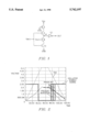
- FIG. 1 is a circuit diagram of a boosting voltage level detector constructed in accordance with a preferred embodiment of the present invention.
- FIG. 2 is a timing diagram illustrating the timing of the conventional boosting circuit and the boosting circuit according to the present invention.
- the boosting voltage level detector depicted in FIG. 1 includes a PMOS transistor 2 and three NMOS transistors 4, 8, and 10, connected in series between a power supply voltage Vcc and ground.
- the gate electrode of the PMOS transistor 2 is coupled to ground.
- the gate electrode of the NMOS transistor 8 is coupled to the power supply voltage Vcc.
- the gate electrodes of the NMOS transistors 4 and 10 are commonly coupled to the boosting voltage Vpp.
- the boosting voltage level detector has an output node 6 intermediate the NMOS transistors 4 and 8, which is coupled to an inverter 12, whose output, labelled OUT, and termed oscillator enable signal, is coupled to an oscillator (not shown) of a pumping circuit (not shown) which generates the boosting voltage Vpp.
- the PMOS transistor 2 functions as a current source
- the NMOS transistor 8 functions as a resistor.
- the PMOS transistor 2 and the NMOS transistor 4 connected in series between the power supply voltage Vcc and the output node 6 constitute a pull-up portion of the circuit
- the NMOS transistors 8 and 10 connected in series between the output node 6 and ground constitute a pull-down portion of the circuit.
- this circuit is capable of quickly and accurately detecting when the boosting voltage Vpp exceeds or falls below a predetermined voltage level, e.g., 2Vcc.
- the boosting voltage level detector of the present invention operates in the following manner. More particularly, the current flow through the NMOS transistors 4 and 10 of the pull-up and pull-down portions of the circuit, respectively, is controlled by the boosting voltage Vpp.
- the NMOS transistors 4 and 10 are each constructed to have a threshold voltage whose level is such that when the boosting voltage Vpp applied to the gate electrodes thereof rises above the predetermined voltage, e.g., 2Vcc, they are turned on, and when the boosting voltage Vpp falls below the predetermined voltage, they are turned off.
- the NMOS transistor 4 has a variable resistance R4 whose value is controlled by the boosting voltage Vpp
- the NMOS transistor 10 has a variable resistance R10 whose value is also controlled by the boosting voltage Vpp.
- the voltage at the output node 6 has a value which is determined by the resistance ratio R10/(R4+R10).
- the boosting level detection signal which appears at the output node 6, is inverted and amplified by the inverter 12 (which can be comprised of a chain of inverters).
- the oscillator enable signal output by the inverter 12 is utilized to start and stop the oscillator (not shown) of the pumping circuit (not shown) which produces the boosting voltage Vpp.
Landscapes
- Engineering & Computer Science (AREA)
- Physics & Mathematics (AREA)
- Power Engineering (AREA)
- General Physics & Mathematics (AREA)
- Microelectronics & Electronic Packaging (AREA)
- Nonlinear Science (AREA)
- Condensed Matter Physics & Semiconductors (AREA)
- Computer Hardware Design (AREA)
- Dram (AREA)
Abstract
Description
Claims (21)
Applications Claiming Priority (2)
| Application Number | Priority Date | Filing Date | Title |
|---|---|---|---|
| KR1019930024669A KR0124046B1 (en) | 1993-11-18 | 1993-11-18 | Vpp detector of semiconductor memory device |
| KR24669/1993 | 1993-11-18 |
Publications (1)
| Publication Number | Publication Date |
|---|---|
| US5742197A true US5742197A (en) | 1998-04-21 |
Family
ID=19368454
Family Applications (1)
| Application Number | Title | Priority Date | Filing Date |
|---|---|---|---|
| US08/341,108 Expired - Lifetime US5742197A (en) | 1993-11-18 | 1994-11-18 | Boosting voltage level detector for a semiconductor memory device |
Country Status (2)
| Country | Link |
|---|---|
| US (1) | US5742197A (en) |
| KR (1) | KR0124046B1 (en) |
Cited By (4)
| Publication number | Priority date | Publication date | Assignee | Title |
|---|---|---|---|---|
| US5821806A (en) * | 1996-01-24 | 1998-10-13 | Sgs-Thomson Microelectronics Srl. | Boost regulator |
| US6262621B1 (en) * | 1999-04-27 | 2001-07-17 | Samsung Electronics Co., Ltd. | Voltage boosting circuit for semiconductor device |
| US6342808B1 (en) | 1999-09-17 | 2002-01-29 | Samsung Electronics Co., Ltd. | High voltage generating circuit |
| US20060290412A1 (en) * | 2005-06-28 | 2006-12-28 | Samsung Electronics Co., Ltd. | Substrate bias voltage generating circuit for use in a semiconductor memory device |
Citations (25)
| Publication number | Priority date | Publication date | Assignee | Title |
|---|---|---|---|---|
| US3914702A (en) * | 1973-06-01 | 1975-10-21 | Rca Corp | Complementary field-effect transistor amplifier |
| US4663584A (en) * | 1985-06-10 | 1987-05-05 | Kabushiki Kaisha Toshiba | Intermediate potential generation circuit |
| US4782247A (en) * | 1984-08-08 | 1988-11-01 | Fujitsu Limited | Decoder circuit having a variable power supply |
| US4794278A (en) * | 1987-12-30 | 1988-12-27 | Intel Corporation | Stable substrate bias generator for MOS circuits |
| US4820936A (en) * | 1987-05-29 | 1989-04-11 | U.S. Philips Corp. | Integrated CMOS circuit comprising a substrate bias voltage generator |
| US4947064A (en) * | 1988-06-09 | 1990-08-07 | Samsung Electronic Co., Ltd. | Semiconductor device having a time delay function |
| US4961007A (en) * | 1988-12-08 | 1990-10-02 | Mitsubishi Denki Kabushiki Kaisha | Substrate bias potential generator of a semiconductor integrated circuit device and a generating method therefor |
| US4967103A (en) * | 1988-02-01 | 1990-10-30 | U.S. Philips Corp. | Integrated logic circuit with protector transistor |
| US4983860A (en) * | 1988-04-12 | 1991-01-08 | Samsung Electronics Co., Ltd. | Data output buffer for use in semiconductor device |
| US4988894A (en) * | 1988-06-16 | 1991-01-29 | Kabushiki Kaisha Toshiba | Power supply switching circuit |
| US5072134A (en) * | 1989-06-10 | 1991-12-10 | Samsung Electronics Co., Ltd. | Internal voltage converter in semiconductor integrated circuit |
| US5128560A (en) * | 1991-03-22 | 1992-07-07 | Micron Technology, Inc. | Boosted supply output driver circuit for driving an all N-channel output stage |
| US5202587A (en) * | 1990-12-20 | 1993-04-13 | Micron Technology, Inc. | MOSFET gate substrate bias sensor |
| US5208488A (en) * | 1989-03-03 | 1993-05-04 | Kabushiki Kaisha Toshiba | Potential detecting circuit |
| USRE34290E (en) * | 1985-03-27 | 1993-06-22 | Mitsubishi Denki K.K. | Constant voltage generating circuit |
| US5264808A (en) * | 1991-02-27 | 1993-11-23 | Kabushiki Kaisha Toshiba | Substrate potential adjusting apparatus |
| US5270584A (en) * | 1991-08-26 | 1993-12-14 | Nec Corporation | Semiconductor integrated circuit |
| US5278460A (en) * | 1992-04-07 | 1994-01-11 | Micron Technology, Inc. | Voltage compensating CMOS input buffer |
| US5296801A (en) * | 1991-07-29 | 1994-03-22 | Kabushiki Kaisha Toshiba | Bias voltage generating circuit |
| US5336952A (en) * | 1988-09-02 | 1994-08-09 | Kabushiki Kaisha Toshiba | Semiconductor integrated circuit protected from element breakdown by reducing the electric field between the gate and drain or source of a field effect transistor |
| US5341045A (en) * | 1992-11-06 | 1994-08-23 | Intel Corporation | Programmable input buffer |
| US5355033A (en) * | 1991-05-24 | 1994-10-11 | Samsung Electronics Co., Ltd. | Data input buffer circuit for use in a semiconductor memory device |
| US5367489A (en) * | 1991-11-07 | 1994-11-22 | Samsung Electronics Co., Ltd. | Voltage pumping circuit for semiconductor memory devices |
| US5389842A (en) * | 1992-08-10 | 1995-02-14 | Nippon Steel Semiconductor Corporation | Latch-up immune CMOS output driver |
| US5493244A (en) * | 1994-01-13 | 1996-02-20 | Atmel Corporation | Breakdown protection circuit using high voltage detection |
-
1993
- 1993-11-18 KR KR1019930024669A patent/KR0124046B1/en not_active IP Right Cessation
-
1994
- 1994-11-18 US US08/341,108 patent/US5742197A/en not_active Expired - Lifetime
Patent Citations (27)
| Publication number | Priority date | Publication date | Assignee | Title |
|---|---|---|---|---|
| US3914702A (en) * | 1973-06-01 | 1975-10-21 | Rca Corp | Complementary field-effect transistor amplifier |
| US4782247A (en) * | 1984-08-08 | 1988-11-01 | Fujitsu Limited | Decoder circuit having a variable power supply |
| USRE34290E (en) * | 1985-03-27 | 1993-06-22 | Mitsubishi Denki K.K. | Constant voltage generating circuit |
| US4663584B1 (en) * | 1985-06-10 | 1996-05-21 | Toshiba Kk | Intermediate potential generation circuit |
| US4663584A (en) * | 1985-06-10 | 1987-05-05 | Kabushiki Kaisha Toshiba | Intermediate potential generation circuit |
| US4820936A (en) * | 1987-05-29 | 1989-04-11 | U.S. Philips Corp. | Integrated CMOS circuit comprising a substrate bias voltage generator |
| US4794278A (en) * | 1987-12-30 | 1988-12-27 | Intel Corporation | Stable substrate bias generator for MOS circuits |
| US4967103A (en) * | 1988-02-01 | 1990-10-30 | U.S. Philips Corp. | Integrated logic circuit with protector transistor |
| US4983860A (en) * | 1988-04-12 | 1991-01-08 | Samsung Electronics Co., Ltd. | Data output buffer for use in semiconductor device |
| US4947064A (en) * | 1988-06-09 | 1990-08-07 | Samsung Electronic Co., Ltd. | Semiconductor device having a time delay function |
| US4988894A (en) * | 1988-06-16 | 1991-01-29 | Kabushiki Kaisha Toshiba | Power supply switching circuit |
| US5336952A (en) * | 1988-09-02 | 1994-08-09 | Kabushiki Kaisha Toshiba | Semiconductor integrated circuit protected from element breakdown by reducing the electric field between the gate and drain or source of a field effect transistor |
| US4961007A (en) * | 1988-12-08 | 1990-10-02 | Mitsubishi Denki Kabushiki Kaisha | Substrate bias potential generator of a semiconductor integrated circuit device and a generating method therefor |
| US5208488A (en) * | 1989-03-03 | 1993-05-04 | Kabushiki Kaisha Toshiba | Potential detecting circuit |
| US5072134A (en) * | 1989-06-10 | 1991-12-10 | Samsung Electronics Co., Ltd. | Internal voltage converter in semiconductor integrated circuit |
| US5072134B1 (en) * | 1989-06-10 | 1993-08-10 | Min Dong-Sun | |
| US5202587A (en) * | 1990-12-20 | 1993-04-13 | Micron Technology, Inc. | MOSFET gate substrate bias sensor |
| US5264808A (en) * | 1991-02-27 | 1993-11-23 | Kabushiki Kaisha Toshiba | Substrate potential adjusting apparatus |
| US5128560A (en) * | 1991-03-22 | 1992-07-07 | Micron Technology, Inc. | Boosted supply output driver circuit for driving an all N-channel output stage |
| US5355033A (en) * | 1991-05-24 | 1994-10-11 | Samsung Electronics Co., Ltd. | Data input buffer circuit for use in a semiconductor memory device |
| US5296801A (en) * | 1991-07-29 | 1994-03-22 | Kabushiki Kaisha Toshiba | Bias voltage generating circuit |
| US5270584A (en) * | 1991-08-26 | 1993-12-14 | Nec Corporation | Semiconductor integrated circuit |
| US5367489A (en) * | 1991-11-07 | 1994-11-22 | Samsung Electronics Co., Ltd. | Voltage pumping circuit for semiconductor memory devices |
| US5278460A (en) * | 1992-04-07 | 1994-01-11 | Micron Technology, Inc. | Voltage compensating CMOS input buffer |
| US5389842A (en) * | 1992-08-10 | 1995-02-14 | Nippon Steel Semiconductor Corporation | Latch-up immune CMOS output driver |
| US5341045A (en) * | 1992-11-06 | 1994-08-23 | Intel Corporation | Programmable input buffer |
| US5493244A (en) * | 1994-01-13 | 1996-02-20 | Atmel Corporation | Breakdown protection circuit using high voltage detection |
Cited By (6)
| Publication number | Priority date | Publication date | Assignee | Title |
|---|---|---|---|---|
| US5821806A (en) * | 1996-01-24 | 1998-10-13 | Sgs-Thomson Microelectronics Srl. | Boost regulator |
| US6262621B1 (en) * | 1999-04-27 | 2001-07-17 | Samsung Electronics Co., Ltd. | Voltage boosting circuit for semiconductor device |
| DE19961135B4 (en) * | 1999-04-27 | 2010-04-15 | Samsung Electronics Co., Ltd., Suwon | Voltage detector for use in a semiconductor device |
| US6342808B1 (en) | 1999-09-17 | 2002-01-29 | Samsung Electronics Co., Ltd. | High voltage generating circuit |
| US20060290412A1 (en) * | 2005-06-28 | 2006-12-28 | Samsung Electronics Co., Ltd. | Substrate bias voltage generating circuit for use in a semiconductor memory device |
| US7298199B2 (en) * | 2005-06-28 | 2007-11-20 | Samsung Electronics Co., Ltd. | Substrate bias voltage generating circuit for use in a semiconductor memory device |
Also Published As
| Publication number | Publication date |
|---|---|
| KR0124046B1 (en) | 1997-11-25 |
| KR950015748A (en) | 1995-06-17 |
Similar Documents
| Publication | Publication Date | Title |
|---|---|---|
| US6492863B2 (en) | Internal high voltage generation circuit capable of stably generating internal high voltage and circuit element therefor | |
| US4961167A (en) | Substrate bias generator in a dynamic random access memory with auto/self refresh functions and a method of generating a substrate bias therein | |
| US7733132B2 (en) | Bulk bias voltage level detector in semiconductor memory device | |
| US5220221A (en) | Sense amplifier pulldown circuit for minimizing ground noise at high power supply voltages | |
| US5747974A (en) | Internal supply voltage generating circuit for semiconductor memory device | |
| KR100262029B1 (en) | Delay circuit having delay time free from influence of operation environment | |
| JPH04351791A (en) | Data input buffer for semiconductor memory device | |
| EP0576045A2 (en) | Semiconductor memory device | |
| JPS6238591A (en) | Complementary semiconductor memory device | |
| US6778000B2 (en) | Integrated circuit devices that provide constant time delays irrespective of temperature variation | |
| US5532969A (en) | Clocking circuit with increasing delay as supply voltage VDD | |
| US5909394A (en) | Precharge circuit for preventing invalid output pulses caused by current sensing circuits in flash memory devices | |
| KR19990029191A (en) | Semiconductor integrated circuit device with improved low voltage operation | |
| US5742197A (en) | Boosting voltage level detector for a semiconductor memory device | |
| EP0399820B1 (en) | Semiconductor memories | |
| US6867639B2 (en) | Half voltage generator for use in semiconductor memory device | |
| JPH0743933B2 (en) | Transition detection circuit | |
| US5881005A (en) | Semiconductor integrated circuit device having a constant delay-time circuit for different operating voltages | |
| JP3308572B2 (en) | Semiconductor device | |
| US4807193A (en) | Semiconductor memory device with a detection circuit to detect word line potential | |
| EP0905702B1 (en) | Secondery sense amplifier with window discriminator for self-timed operation | |
| KR0154755B1 (en) | Semiconductor memory device having variable plate voltage generater circuit | |
| US6490211B2 (en) | Random access memory device | |
| IE53368B1 (en) | Mos dynamic memory device | |
| US6934204B2 (en) | Semiconductor device with reduced terminal input capacitance |
Legal Events
| Date | Code | Title | Description |
|---|---|---|---|
| AS | Assignment |
Owner name: SAMSUNG ELECTRONICS CO., LTD., KOREA, REPUBLIC OF Free format text: ASSIGNMENT OF ASSIGNORS INTEREST;ASSIGNORS:KIM, HYUNG-DONG;PARK, CHAN-JONG;REEL/FRAME:007302/0522 Effective date: 19941227 |
|
| STCF | Information on status: patent grant |
Free format text: PATENTED CASE |
|
| FEPP | Fee payment procedure |
Free format text: PAYOR NUMBER ASSIGNED (ORIGINAL EVENT CODE: ASPN); ENTITY STATUS OF PATENT OWNER: LARGE ENTITY |
|
| FPAY | Fee payment |
Year of fee payment: 4 |
|
| FPAY | Fee payment |
Year of fee payment: 8 |
|
| FEPP | Fee payment procedure |
Free format text: PAYOR NUMBER ASSIGNED (ORIGINAL EVENT CODE: ASPN); ENTITY STATUS OF PATENT OWNER: LARGE ENTITY Free format text: PAYER NUMBER DE-ASSIGNED (ORIGINAL EVENT CODE: RMPN); ENTITY STATUS OF PATENT OWNER: LARGE ENTITY |
|
| FPAY | Fee payment |
Year of fee payment: 12 |