US5744863A - Chip carrier modules with heat sinks attached by flexible-epoxy - Google Patents
Chip carrier modules with heat sinks attached by flexible-epoxy Download PDFInfo
- Publication number
- US5744863A US5744863A US08/474,341 US47434195A US5744863A US 5744863 A US5744863 A US 5744863A US 47434195 A US47434195 A US 47434195A US 5744863 A US5744863 A US 5744863A
- Authority
- US
- United States
- Prior art keywords
- substrate
- chip
- epoxy
- flexible
- heat spreader
- Prior art date
- Legal status (The legal status is an assumption and is not a legal conclusion. Google has not performed a legal analysis and makes no representation as to the accuracy of the status listed.)
- Expired - Lifetime
Links
Images


Classifications
-
- H—ELECTRICITY
- H01—ELECTRIC ELEMENTS
- H01L—SEMICONDUCTOR DEVICES NOT COVERED BY CLASS H10
- H01L23/00—Details of semiconductor or other solid state devices
- H01L23/34—Arrangements for cooling, heating, ventilating or temperature compensation ; Temperature sensing arrangements
- H01L23/36—Selection of materials, or shaping, to facilitate cooling or heating, e.g. heatsinks
-
- H—ELECTRICITY
- H01—ELECTRIC ELEMENTS
- H01L—SEMICONDUCTOR DEVICES NOT COVERED BY CLASS H10
- H01L21/00—Processes or apparatus adapted for the manufacture or treatment of semiconductor or solid state devices or of parts thereof
- H01L21/02—Manufacture or treatment of semiconductor devices or of parts thereof
- H01L21/04—Manufacture or treatment of semiconductor devices or of parts thereof the devices having at least one potential-jump barrier or surface barrier, e.g. PN junction, depletion layer or carrier concentration layer
- H01L21/50—Assembly of semiconductor devices using processes or apparatus not provided for in a single one of the subgroups H01L21/06 - H01L21/326, e.g. sealing of a cap to a base of a container
- H01L21/56—Encapsulations, e.g. encapsulation layers, coatings
- H01L21/563—Encapsulation of active face of flip-chip device, e.g. underfilling or underencapsulation of flip-chip, encapsulation preform on chip or mounting substrate
-
- H—ELECTRICITY
- H01—ELECTRIC ELEMENTS
- H01L—SEMICONDUCTOR DEVICES NOT COVERED BY CLASS H10
- H01L23/00—Details of semiconductor or other solid state devices
- H01L23/28—Encapsulations, e.g. encapsulating layers, coatings, e.g. for protection
- H01L23/31—Encapsulations, e.g. encapsulating layers, coatings, e.g. for protection characterised by the arrangement or shape
- H01L23/3107—Encapsulations, e.g. encapsulating layers, coatings, e.g. for protection characterised by the arrangement or shape the device being completely enclosed
- H01L23/3121—Encapsulations, e.g. encapsulating layers, coatings, e.g. for protection characterised by the arrangement or shape the device being completely enclosed a substrate forming part of the encapsulation
- H01L23/3128—Encapsulations, e.g. encapsulating layers, coatings, e.g. for protection characterised by the arrangement or shape the device being completely enclosed a substrate forming part of the encapsulation the substrate having spherical bumps for external connection
-
- H—ELECTRICITY
- H01—ELECTRIC ELEMENTS
- H01L—SEMICONDUCTOR DEVICES NOT COVERED BY CLASS H10
- H01L23/00—Details of semiconductor or other solid state devices
- H01L23/34—Arrangements for cooling, heating, ventilating or temperature compensation ; Temperature sensing arrangements
- H01L23/36—Selection of materials, or shaping, to facilitate cooling or heating, e.g. heatsinks
- H01L23/367—Cooling facilitated by shape of device
-
- H—ELECTRICITY
- H01—ELECTRIC ELEMENTS
- H01L—SEMICONDUCTOR DEVICES NOT COVERED BY CLASS H10
- H01L23/00—Details of semiconductor or other solid state devices
- H01L23/34—Arrangements for cooling, heating, ventilating or temperature compensation ; Temperature sensing arrangements
- H01L23/36—Selection of materials, or shaping, to facilitate cooling or heating, e.g. heatsinks
- H01L23/373—Cooling facilitated by selection of materials for the device or materials for thermal expansion adaptation, e.g. carbon
- H01L23/3737—Organic materials with or without a thermoconductive filler
-
- H—ELECTRICITY
- H01—ELECTRIC ELEMENTS
- H01L—SEMICONDUCTOR DEVICES NOT COVERED BY CLASS H10
- H01L23/00—Details of semiconductor or other solid state devices
- H01L23/34—Arrangements for cooling, heating, ventilating or temperature compensation ; Temperature sensing arrangements
- H01L23/42—Fillings or auxiliary members in containers or encapsulations selected or arranged to facilitate heating or cooling
-
- H—ELECTRICITY
- H01—ELECTRIC ELEMENTS
- H01L—SEMICONDUCTOR DEVICES NOT COVERED BY CLASS H10
- H01L2224/00—Indexing scheme for arrangements for connecting or disconnecting semiconductor or solid-state bodies and methods related thereto as covered by H01L24/00
- H01L2224/01—Means for bonding being attached to, or being formed on, the surface to be connected, e.g. chip-to-package, die-attach, "first-level" interconnects; Manufacturing methods related thereto
- H01L2224/10—Bump connectors; Manufacturing methods related thereto
- H01L2224/15—Structure, shape, material or disposition of the bump connectors after the connecting process
- H01L2224/16—Structure, shape, material or disposition of the bump connectors after the connecting process of an individual bump connector
- H01L2224/161—Disposition
- H01L2224/16151—Disposition the bump connector connecting between a semiconductor or solid-state body and an item not being a semiconductor or solid-state body, e.g. chip-to-substrate, chip-to-passive
- H01L2224/16221—Disposition the bump connector connecting between a semiconductor or solid-state body and an item not being a semiconductor or solid-state body, e.g. chip-to-substrate, chip-to-passive the body and the item being stacked
- H01L2224/16225—Disposition the bump connector connecting between a semiconductor or solid-state body and an item not being a semiconductor or solid-state body, e.g. chip-to-substrate, chip-to-passive the body and the item being stacked the item being non-metallic, e.g. insulating substrate with or without metallisation
-
- H—ELECTRICITY
- H01—ELECTRIC ELEMENTS
- H01L—SEMICONDUCTOR DEVICES NOT COVERED BY CLASS H10
- H01L2224/00—Indexing scheme for arrangements for connecting or disconnecting semiconductor or solid-state bodies and methods related thereto as covered by H01L24/00
- H01L2224/01—Means for bonding being attached to, or being formed on, the surface to be connected, e.g. chip-to-package, die-attach, "first-level" interconnects; Manufacturing methods related thereto
- H01L2224/26—Layer connectors, e.g. plate connectors, solder or adhesive layers; Manufacturing methods related thereto
- H01L2224/31—Structure, shape, material or disposition of the layer connectors after the connecting process
- H01L2224/32—Structure, shape, material or disposition of the layer connectors after the connecting process of an individual layer connector
- H01L2224/321—Disposition
- H01L2224/32151—Disposition the layer connector connecting between a semiconductor or solid-state body and an item not being a semiconductor or solid-state body, e.g. chip-to-substrate, chip-to-passive
- H01L2224/32221—Disposition the layer connector connecting between a semiconductor or solid-state body and an item not being a semiconductor or solid-state body, e.g. chip-to-substrate, chip-to-passive the body and the item being stacked
- H01L2224/32225—Disposition the layer connector connecting between a semiconductor or solid-state body and an item not being a semiconductor or solid-state body, e.g. chip-to-substrate, chip-to-passive the body and the item being stacked the item being non-metallic, e.g. insulating substrate with or without metallisation
-
- H—ELECTRICITY
- H01—ELECTRIC ELEMENTS
- H01L—SEMICONDUCTOR DEVICES NOT COVERED BY CLASS H10
- H01L2224/00—Indexing scheme for arrangements for connecting or disconnecting semiconductor or solid-state bodies and methods related thereto as covered by H01L24/00
- H01L2224/01—Means for bonding being attached to, or being formed on, the surface to be connected, e.g. chip-to-package, die-attach, "first-level" interconnects; Manufacturing methods related thereto
- H01L2224/42—Wire connectors; Manufacturing methods related thereto
- H01L2224/47—Structure, shape, material or disposition of the wire connectors after the connecting process
- H01L2224/48—Structure, shape, material or disposition of the wire connectors after the connecting process of an individual wire connector
- H01L2224/4805—Shape
- H01L2224/4809—Loop shape
- H01L2224/48091—Arched
-
- H—ELECTRICITY
- H01—ELECTRIC ELEMENTS
- H01L—SEMICONDUCTOR DEVICES NOT COVERED BY CLASS H10
- H01L2224/00—Indexing scheme for arrangements for connecting or disconnecting semiconductor or solid-state bodies and methods related thereto as covered by H01L24/00
- H01L2224/01—Means for bonding being attached to, or being formed on, the surface to be connected, e.g. chip-to-package, die-attach, "first-level" interconnects; Manufacturing methods related thereto
- H01L2224/42—Wire connectors; Manufacturing methods related thereto
- H01L2224/47—Structure, shape, material or disposition of the wire connectors after the connecting process
- H01L2224/48—Structure, shape, material or disposition of the wire connectors after the connecting process of an individual wire connector
- H01L2224/481—Disposition
- H01L2224/48151—Connecting between a semiconductor or solid-state body and an item not being a semiconductor or solid-state body, e.g. chip-to-substrate, chip-to-passive
- H01L2224/48221—Connecting between a semiconductor or solid-state body and an item not being a semiconductor or solid-state body, e.g. chip-to-substrate, chip-to-passive the body and the item being stacked
- H01L2224/48245—Connecting between a semiconductor or solid-state body and an item not being a semiconductor or solid-state body, e.g. chip-to-substrate, chip-to-passive the body and the item being stacked the item being metallic
- H01L2224/48247—Connecting between a semiconductor or solid-state body and an item not being a semiconductor or solid-state body, e.g. chip-to-substrate, chip-to-passive the body and the item being stacked the item being metallic connecting the wire to a bond pad of the item
-
- H—ELECTRICITY
- H01—ELECTRIC ELEMENTS
- H01L—SEMICONDUCTOR DEVICES NOT COVERED BY CLASS H10
- H01L2224/00—Indexing scheme for arrangements for connecting or disconnecting semiconductor or solid-state bodies and methods related thereto as covered by H01L24/00
- H01L2224/73—Means for bonding being of different types provided for in two or more of groups H01L2224/10, H01L2224/18, H01L2224/26, H01L2224/34, H01L2224/42, H01L2224/50, H01L2224/63, H01L2224/71
- H01L2224/732—Location after the connecting process
- H01L2224/73201—Location after the connecting process on the same surface
- H01L2224/73203—Bump and layer connectors
- H01L2224/73204—Bump and layer connectors the bump connector being embedded into the layer connector
-
- H—ELECTRICITY
- H01—ELECTRIC ELEMENTS
- H01L—SEMICONDUCTOR DEVICES NOT COVERED BY CLASS H10
- H01L2224/00—Indexing scheme for arrangements for connecting or disconnecting semiconductor or solid-state bodies and methods related thereto as covered by H01L24/00
- H01L2224/73—Means for bonding being of different types provided for in two or more of groups H01L2224/10, H01L2224/18, H01L2224/26, H01L2224/34, H01L2224/42, H01L2224/50, H01L2224/63, H01L2224/71
- H01L2224/732—Location after the connecting process
- H01L2224/73251—Location after the connecting process on different surfaces
- H01L2224/73253—Bump and layer connectors
-
- H—ELECTRICITY
- H01—ELECTRIC ELEMENTS
- H01L—SEMICONDUCTOR DEVICES NOT COVERED BY CLASS H10
- H01L2224/00—Indexing scheme for arrangements for connecting or disconnecting semiconductor or solid-state bodies and methods related thereto as covered by H01L24/00
- H01L2224/73—Means for bonding being of different types provided for in two or more of groups H01L2224/10, H01L2224/18, H01L2224/26, H01L2224/34, H01L2224/42, H01L2224/50, H01L2224/63, H01L2224/71
- H01L2224/732—Location after the connecting process
- H01L2224/73251—Location after the connecting process on different surfaces
- H01L2224/73265—Layer and wire connectors
-
- H—ELECTRICITY
- H01—ELECTRIC ELEMENTS
- H01L—SEMICONDUCTOR DEVICES NOT COVERED BY CLASS H10
- H01L24/00—Arrangements for connecting or disconnecting semiconductor or solid-state bodies; Methods or apparatus related thereto
- H01L24/01—Means for bonding being attached to, or being formed on, the surface to be connected, e.g. chip-to-package, die-attach, "first-level" interconnects; Manufacturing methods related thereto
- H01L24/42—Wire connectors; Manufacturing methods related thereto
- H01L24/47—Structure, shape, material or disposition of the wire connectors after the connecting process
- H01L24/48—Structure, shape, material or disposition of the wire connectors after the connecting process of an individual wire connector
-
- H—ELECTRICITY
- H01—ELECTRIC ELEMENTS
- H01L—SEMICONDUCTOR DEVICES NOT COVERED BY CLASS H10
- H01L2924/00—Indexing scheme for arrangements or methods for connecting or disconnecting semiconductor or solid-state bodies as covered by H01L24/00
- H01L2924/0001—Technical content checked by a classifier
- H01L2924/00014—Technical content checked by a classifier the subject-matter covered by the group, the symbol of which is combined with the symbol of this group, being disclosed without further technical details
-
- H—ELECTRICITY
- H01—ELECTRIC ELEMENTS
- H01L—SEMICONDUCTOR DEVICES NOT COVERED BY CLASS H10
- H01L2924/00—Indexing scheme for arrangements or methods for connecting or disconnecting semiconductor or solid-state bodies as covered by H01L24/00
- H01L2924/01—Chemical elements
- H01L2924/01078—Platinum [Pt]
-
- H—ELECTRICITY
- H01—ELECTRIC ELEMENTS
- H01L—SEMICONDUCTOR DEVICES NOT COVERED BY CLASS H10
- H01L2924/00—Indexing scheme for arrangements or methods for connecting or disconnecting semiconductor or solid-state bodies as covered by H01L24/00
- H01L2924/013—Alloys
- H01L2924/0132—Binary Alloys
- H01L2924/01322—Eutectic Alloys, i.e. obtained by a liquid transforming into two solid phases
-
- H—ELECTRICITY
- H01—ELECTRIC ELEMENTS
- H01L—SEMICONDUCTOR DEVICES NOT COVERED BY CLASS H10
- H01L2924/00—Indexing scheme for arrangements or methods for connecting or disconnecting semiconductor or solid-state bodies as covered by H01L24/00
- H01L2924/10—Details of semiconductor or other solid state devices to be connected
- H01L2924/102—Material of the semiconductor or solid state bodies
- H01L2924/1025—Semiconducting materials
- H01L2924/10251—Elemental semiconductors, i.e. Group IV
- H01L2924/10253—Silicon [Si]
-
- H—ELECTRICITY
- H01—ELECTRIC ELEMENTS
- H01L—SEMICONDUCTOR DEVICES NOT COVERED BY CLASS H10
- H01L2924/00—Indexing scheme for arrangements or methods for connecting or disconnecting semiconductor or solid-state bodies as covered by H01L24/00
- H01L2924/10—Details of semiconductor or other solid state devices to be connected
- H01L2924/11—Device type
- H01L2924/12—Passive devices, e.g. 2 terminal devices
- H01L2924/1204—Optical Diode
- H01L2924/12042—LASER
-
- H—ELECTRICITY
- H01—ELECTRIC ELEMENTS
- H01L—SEMICONDUCTOR DEVICES NOT COVERED BY CLASS H10
- H01L2924/00—Indexing scheme for arrangements or methods for connecting or disconnecting semiconductor or solid-state bodies as covered by H01L24/00
- H01L2924/10—Details of semiconductor or other solid state devices to be connected
- H01L2924/11—Device type
- H01L2924/12—Passive devices, e.g. 2 terminal devices
- H01L2924/1204—Optical Diode
- H01L2924/12044—OLED
-
- H—ELECTRICITY
- H01—ELECTRIC ELEMENTS
- H01L—SEMICONDUCTOR DEVICES NOT COVERED BY CLASS H10
- H01L2924/00—Indexing scheme for arrangements or methods for connecting or disconnecting semiconductor or solid-state bodies as covered by H01L24/00
- H01L2924/15—Details of package parts other than the semiconductor or other solid state devices to be connected
- H01L2924/151—Die mounting substrate
- H01L2924/1515—Shape
- H01L2924/15153—Shape the die mounting substrate comprising a recess for hosting the device
-
- H—ELECTRICITY
- H01—ELECTRIC ELEMENTS
- H01L—SEMICONDUCTOR DEVICES NOT COVERED BY CLASS H10
- H01L2924/00—Indexing scheme for arrangements or methods for connecting or disconnecting semiconductor or solid-state bodies as covered by H01L24/00
- H01L2924/15—Details of package parts other than the semiconductor or other solid state devices to be connected
- H01L2924/151—Die mounting substrate
- H01L2924/1517—Multilayer substrate
-
- H—ELECTRICITY
- H01—ELECTRIC ELEMENTS
- H01L—SEMICONDUCTOR DEVICES NOT COVERED BY CLASS H10
- H01L2924/00—Indexing scheme for arrangements or methods for connecting or disconnecting semiconductor or solid-state bodies as covered by H01L24/00
- H01L2924/15—Details of package parts other than the semiconductor or other solid state devices to be connected
- H01L2924/151—Die mounting substrate
- H01L2924/153—Connection portion
- H01L2924/1531—Connection portion the connection portion being formed only on the surface of the substrate opposite to the die mounting surface
- H01L2924/15311—Connection portion the connection portion being formed only on the surface of the substrate opposite to the die mounting surface being a ball array, e.g. BGA
-
- H—ELECTRICITY
- H01—ELECTRIC ELEMENTS
- H01L—SEMICONDUCTOR DEVICES NOT COVERED BY CLASS H10
- H01L2924/00—Indexing scheme for arrangements or methods for connecting or disconnecting semiconductor or solid-state bodies as covered by H01L24/00
- H01L2924/15—Details of package parts other than the semiconductor or other solid state devices to be connected
- H01L2924/151—Die mounting substrate
- H01L2924/153—Connection portion
- H01L2924/1531—Connection portion the connection portion being formed only on the surface of the substrate opposite to the die mounting surface
- H01L2924/15312—Connection portion the connection portion being formed only on the surface of the substrate opposite to the die mounting surface being a pin array, e.g. PGA
-
- H—ELECTRICITY
- H01—ELECTRIC ELEMENTS
- H01L—SEMICONDUCTOR DEVICES NOT COVERED BY CLASS H10
- H01L2924/00—Indexing scheme for arrangements or methods for connecting or disconnecting semiconductor or solid-state bodies as covered by H01L24/00
- H01L2924/15—Details of package parts other than the semiconductor or other solid state devices to be connected
- H01L2924/151—Die mounting substrate
- H01L2924/153—Connection portion
- H01L2924/1532—Connection portion the connection portion being formed on the die mounting surface of the substrate
-
- H—ELECTRICITY
- H01—ELECTRIC ELEMENTS
- H01L—SEMICONDUCTOR DEVICES NOT COVERED BY CLASS H10
- H01L2924/00—Indexing scheme for arrangements or methods for connecting or disconnecting semiconductor or solid-state bodies as covered by H01L24/00
- H01L2924/15—Details of package parts other than the semiconductor or other solid state devices to be connected
- H01L2924/151—Die mounting substrate
- H01L2924/156—Material
- H01L2924/157—Material with a principal constituent of the material being a metal or a metalloid, e.g. boron [B], silicon [Si], germanium [Ge], arsenic [As], antimony [Sb], tellurium [Te] and polonium [Po], and alloys thereof
- H01L2924/15738—Material with a principal constituent of the material being a metal or a metalloid, e.g. boron [B], silicon [Si], germanium [Ge], arsenic [As], antimony [Sb], tellurium [Te] and polonium [Po], and alloys thereof the principal constituent melting at a temperature of greater than or equal to 950 C and less than 1550 C
- H01L2924/15747—Copper [Cu] as principal constituent
-
- H—ELECTRICITY
- H01—ELECTRIC ELEMENTS
- H01L—SEMICONDUCTOR DEVICES NOT COVERED BY CLASS H10
- H01L2924/00—Indexing scheme for arrangements or methods for connecting or disconnecting semiconductor or solid-state bodies as covered by H01L24/00
- H01L2924/15—Details of package parts other than the semiconductor or other solid state devices to be connected
- H01L2924/161—Cap
- H01L2924/1615—Shape
- H01L2924/16195—Flat cap [not enclosing an internal cavity]
-
- H—ELECTRICITY
- H01—ELECTRIC ELEMENTS
- H01L—SEMICONDUCTOR DEVICES NOT COVERED BY CLASS H10
- H01L2924/00—Indexing scheme for arrangements or methods for connecting or disconnecting semiconductor or solid-state bodies as covered by H01L24/00
- H01L2924/15—Details of package parts other than the semiconductor or other solid state devices to be connected
- H01L2924/181—Encapsulation
Definitions
- These inventions relate to the field of heat spreaders and heat sinks for electronic components and the process of attaching such heat spreaders and heat sinks to such components.
- Flip-chips have been thermally connected to heat spreaders using thermal grease as described in U.S. Pat. No. 4,000,509 to Jarvela.
- a heat spreader such as a cap, heat spreader plate, finned heat spreader, or liquid cored cold plate is mechanically connected to a chip carrier module or a circuit board so as to leave a thin gap between a flip-chip attached to the module or board and one surface of the heat spreader.
- This gap is filled with the thermal grease such as a silicone grease which may be filled with a highly thermally conductive material such as silver or ceramic material such as alumina to provide a high quality thermally conductive path between the chip and heat spreader.
- Epoxies have been used to attach semiconductor chips to certain substrates.
- epoxy is used to connect the back of a semiconductor computer chip to a copper clad Invar (Cu-Invar-Cu) interposer which has a coefficient of thermal expansion (CTE) between that of a semiconductor and a glass fiber epoxy circuit board to which the interposer is attached by soldering.
- the circuit board is made of a material (e.g. INVAR) with a CTE that closely matches that of a semiconductor chip, the chip may be directly attached to the board using thermally conductive epoxy.
- a material e.g. INVAR
- 4,914,551 to Anschel discloses attaching a semiconductor chip to a heat spreader of silicon carbide (SiC), aluminum nitride (AlN), or Cu-Invar-Cu using epoxy filled with diamond particles so that CTEs differ by no more than two parts per million per degree Centigrade (ppm/° C.).
- the CTE in ppm/° C. of Si is 2.6, of SiC 2.6, of AlN 4.6, of Invar 2, of Cu-Invar-Cu 3-6, of epoxy 50-80, of fiberglass-epoxy 11-18, and of epoxy filled with fused quarts 5-7.
- Epoxies have been used to encapsulate flip-chip connections as described in U.S. Pat. No. 4,604,644 to Beckham and U.S. Pat. Nos. 4,999,699 and 5,089,440 to Christie, in order to reduce stresses in the C4 (controlled collapse chip connection) joints. C4 joints are described in U.S. Pat. No. 3,458,925. Epoxies for such purposes are well known as described in U.S. Pat. No. 4,701,482 to Itoh. Such epoxies typically have a glass transition temperature (Tg) of about 140°-150° C., and a modulus of around 1,000,000 psi or more.
- Tg glass transition temperature
- Epoxies have been used for transfer molding and injection molding to produce components such as QFPs (quad flat packs), DIPs (dual-in-line packages) and other plastic packages. Ceramic chip carrier packages such as ceramic quad flat packs are typically two ceramic parts connected together with epoxy. ECA (electrically conductive adhesive) chip attachments may be encapsulated with epoxy or more preferrably by a thermoplastic.
- Heat spreaders such as Aluminum (Al) which may be coated by chromate conversion or anodized, or copper (Cu) which may be coated by nickle (Ni), are bonded to plastic packages using epoxy.
- the CTE in ppm/° C. of Al is 23 and of Cu is 17.
- ceramic chip packages are used and silicone adhesives are used to bond a heat spreader to the top of the module or the heat spreader is mechanically attached by: screws or by clipping.
- a "technical data sheet for Ablebond P1-897 of September 1993 recommends attaching a large die to a silver coated copper lead frame using this material.
- a product data sheet for Prima-Bond TM EG 7655 recommends using the material "for bonding materials with highly mismatched CTEs (i.e., Alumina to Aluminum, Silocon to Copper, etc.)
- CQFPs ceramic QFPs
- flip-chip carrier modules such as: capless CQFPs; TBGA (TAB ball grid array), TAB (tape automated bonding) modules as described by Desai and in U.S. Pat. No. 4,681,654 to Clementi, and 5,203,075 to Flynn; CBGA (ceramic ball grid array) modules described by Behum, and in Ser. No. 08/144,981 by Hoebner; DCAM (direct chip attach modules) described in Ser. No. 08/178,994 by White; and well known CPGA (ceramic pin grid array) modules.
- CQFPs ceramic QFPs
- TBGA TAB ball grid array
- TAB tape automated bonding
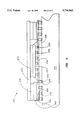
- FIG. 1 shows an aluminum heat spreader bonded by flexible-epoxy to a CQFP to illustrate an embodiment of the invention.
- FIG. 2 shows an aluminum heat spreader bonded by flexible-epoxy to a semiconductor flip-chip on a capless CQFP to illustrate another embodiment of the invention.
- FIG. 3 shows an aluminum heat spreader bonded by flexible-epoxy to a semiconductor flip-chip on a CPGA to illustrate another embodiment of the invention.
- FIG. 4 shows another embodiment of the invention similar to FIG. 3 and in which an aluminum heat spreader is bonded to a semiconductor flip-chip by flexible-epoxy to a CBGA or PBGA.
- FIG. 5 shows a copper heat spreader plate bonded by flexible-epoxy to a semiconductor chip on a tape ball grid array package to illustrate another embodiment of the invention.
- FIG. 6 shows an aluminum heat spreader bonded by flexible-epoxy to a semiconductor chip on a direct chip attachment organic carrier to illustrate another embodiment of the invention.
- FIG. 7 shows the information handling system of the invention which is enhanced by the thermal perfomance provided by bonding heat spreaders to A/N ceramic and/or silicon surfaces of high power density components using flexible-epoxy.
- Typical epoxies have a Tg of about 140-150 degrees C, but flexible-epoxies used in these inventions have a Tg below about 250, preferably below 10° C. and more preferably below 0° C. Also, typical epoxieshave a Young's modulus of around 1,000,000 psi, but flexible-epoxies used in these inventions have a Young's modulus below about 100,000 psi, preferably below 50,000 psi, and even more preferably below 20,000 psi.
- a two part flexible-epoxy named EG 7655 is available from AI Technologies Inc. 9 Princess Rd. Lawrencevill, N.J. 08648 and has a Tg of about -25° C.
- a one part flexible-epoxy named ABLEBOND ®P1-8971 is distributed by Ablestick Laboratories 20021 Susana Road Rancho Dominguez, Calif. 90221. and has a Tg of about 5° C. and a Young's modules of less than about 50,000 psi.
- the CQFP module is produced from two preformed, fired halves 100, 102 of ceramic (preferably Al--N).
- Semiconductor chip 106 preferablysilicon
- top half 100 of the flat pack using for example a typical die attach epoxy 108, and the chip is wire bonded 112 to the lead frame.
- top half 100 is bonded to bottom half 102 using for example a typical epoxy 110, 114.
- Cavity 116 is typically empty but may contain an electrically non-conductive, thermally conductive thermal substance (e.g. silicon grease).
- an Al heat spreader 118 preferably coated by anodization or more preferably by Chromate conversion
- the CTE of Al--N is about 4.6 ppm/° C.
- the CTE of the Al of theheat spreader is about 23.6 ppm/° C., which results in a CTE difference of 19 ppm/° C.
- the ceramic top is a relatively smooth surface and any de-lamination or cracking of the epoxy between the packageand heat spreader causes a critical reduction in heat transfer from the chip.
- Silicone based adhesives have Tg's below 25° C. and Young's Moduli below 20,000 pse. However, mechanically, the bonds are about one third to one half the strength of a flexible epoxy.
- cap 102 may be replaced by epoxy encapsulant (gob top) to protect the wire bond chip.
- the epoxy may just cover the chip and wire bonds or it may extend to the circuit board on which the module is mounted.
- an organic material such as fiberglass-epoxy or a laminate of copper and polyimide foils may be substituted for the ceramic of the top half 100.
- FIG. 2 shows another CQFP 148 which does not have a top half.
- the front side (bottom) of a semiconductor flip-chip die 150 is attached to a singlelayer rectangular ceramic chip carrier 152 by perimeter row or a grid arrayof C4 joints 154 that extend from conductive contacts on the chip to conductive contacts on the carrier.
- the chip bumps could be attached to the contacts on the carrier by eutectic solder bumps depositedby plating, solder inject, or transfer from a decal.
- Leads such as gullwingleads 156 are soldered 158 to copper pads along edges (typically all four edges for QFPs) for surface mount connection to substrate 156.
- the bottom end of the leads may bend under the module in a J or even pointed straight down.
- the joints 154 are encapsulated with epoxy 160 and preferably the leads are encapsulated with epoxy 162.
- an epoxy coating 164 is applied so to protect the top layer ceramic circuitry (a conformal coating).
- Heat spreader 164 is attached to the back side of chip150 using a flexible-epoxy 166. Improved mechanical strenth may be obtainedfor heat spreaders that have a footprint much larger than the chip, by bonding the heat spreader to the conformal coating at 168 with the flexible-epoxy or a typical epoxy.
- the CTE of Si is about 2.6 ppm/° C. and the CTE of the Al of the heat spreader is about 23.6 ppm/° C. which results in a CTE difference of 21 ppm/° C.
- the back of the chip is very smooth resulting in a weak mechanical bond and any de-lamination or cracking of the epoxy between the chip and heat spreader causes a critical reduction in heat transfer from the chip.
- Silicone based adhesives have Tg's below 25° C. and Young's Module below 20,000 psi. However, mechanically, the bonds are about one third to one half the strength of a flexible epoxy.
- Electrodes 156 of module 148 are attached to conductive pads 170 (preferably copper) of substrate 156 (a fiberglass-epoxy circuit board or flexible circuit board of laminated copper and polyimide films).
- FIG. 3 shows a CPGA (ceramic pin grid array module) 200.
- the front side (bottom) of a semiconductor flip-chip die 202 is attached to a rectangularceramic chip carrier 204 (single or multi-layer as shown) by a perimeter row or grid array of joints 206 (preferably C4 or ECA).
- a matrix of pins 208 are wave soldered 210 to copper pads 212 on both end of PTHs (plated-through-holes) extending through substrate 214 (e.g. fiberglass epoxy or flexible laminate of copper-polyimide films).
- Joints 206 are encapsulated with epoxy 220 and a conformal coating of epoxy 222 may be deposited on the surface of substrate 204.
- Heat spreader 224 is attached to the back side of chip 202 using flexible-epoxy 226.
- FIG. 4 shows a BGA (ball grid array) module 240 which is similar to the CPGA of FIG. 3.
- Substrate 242 may be ceramic (CBGA) or plastic (PBGA) and may be one or multi-layer. Again, flexible-epoxy 244 is used to attach heat sink 246 to flip-chip 248.
- FIG. 5 shows TBGA module 250.
- the bottom of flip-chip 252 is attached to copper pads 254 of a flexible chip carrier substrate 256 (a laminate typically of one or more patterned copper layers and polyimide sheets) by joints 258 made by C4, thermal compression bonding, or laser welding or bythe SATT (solder attach tape technology).
- Solder balls 258 (preferably 90/10% Pb/Sn) are attached to copper pads 260 of the flexible tape 256 by laser welding, thermal compression bonding, or by depositing eutectic solder on the pads and reflowing with the balls in place.
- Rectangular metal frame 262 such as Al or preferably Cu plated by nickle (Ni), is attached to the flex substrate by adhesive 264 (preferably epoxy).
- Heat spreader 270 is attached to frame 262 by adhesive 272 (preferably epoxy) and is attached to chip 252 by flexible-epoxy 274.
- the heat spreader may be Al treated by Anodization or chromate conversion or preferrably is Cu coated with Ni.
- Module 250 is attached to substrate 280 (such as fiberglass epoxy or a flexible laminate described above) by depositing solder paste (preferably 37/63% Pb/Sn) on copper pads 282, placing the module on the substrate withthe solder balls on the paste, and heating the structure until the paste becomes molten to form joints of solder 284.
- solder paste preferably 37/63% Pb/Sn
- balls 258 and solder 284 may be replaced by an ECA encapsulated by a thermoplastic or thermoset 286, and which is attached to pads 282 by heat and pressure.
- the CTE of Si is about 2.6 ppm/° C. and the CTE of the Cu of the heat spreader is about 17 ppm/° C. which results in a CTE difference of 14.4 ppm/° C.
- the back of the chip is very smooth resulting in a weak mechanical bond and any de-lamination or cracking of the epoxy between the chip and heat spreader causes a criticalreduction in heat transfer from the chip.
- thermal cycling common epoxies quickly fail (de-laminate).
- Si based adhesives also delaminate during a thermal cycling test consisting of 0° to 100° C. for 1,500 cycles, then -25° to 125° C. for 400 cycles, then -40° to 140° C. for 300 cycles required to prove the reliability of joints between these materials.
- the applicants have discovered that flexible-epoxies (e.g. ABLEBOND 8971 and EG 7655) reliably meet the thermal cycling requirements of this test.
- FIG. 6 shows a DCAM module 300.
- Flip-chip 302 is attached to a multi-layer fiberglass epoxy substrate 304.
- Eutectic solder 306 is deposited (by HASL,solder-on-chip, solder inject, by transfer from a stainless steel decal) toconnect between high temperature solder bumps 308 on the bottom of the chipand copper pads 310 on the top surface of the substrate.
- Copper pads 312 are positioned to connect to copper pads on a interconnect structure (organic circuit board as in FIGS. 2 and 5).
- Solder 314 may be provided onpads 312 for reflow soldered attachment.
- Heat spreader 320 is attached to the back side of chip 302 using an flexible-epoxy 322. Improved mechanicalstrenth can be obtained for heat spreaders which extend significantly past the limits of the chip by encapsulating between the heat spreader at 324 and substrate 304 using flexible-epoxy or another well known epoxy.
- FIG. 7 shows a computer network embodiment of the information handling system 350 of the invention.
- Computer systems 352 and 354 are networked together by optic or electrical signal cable 356.
- Systems 352 and 354 haveCPU (central processor unit) modules 358, 360 and memory modules 362 and 364 respectively.
- the modules use flexible-epoxy 366-372 to attach heat sinks to the modules to allow operation at higher power so that the performance of the entire information handling system is enhanced.
- the modules in each system are attached to one or more electrical interconnectstructures 374, 376.
- the interconnect structures are connected to power supplies 378, 380 such as batteries, transformers, or power cords, and maybe connected to other computer devices 382 such as disk drives, other interconnect structures.
- One or more optic or electrical cables 384 or cable connectors is attached to the interconnect structures to provide fordata input and output with computer peripherals 386 such as keyboards, CRTs, modems, sensors, motors, etc..
- these inventions include multi-chip modules having individual heat spreaders on one or multiple chips and/or common heat spreaders each for a plurality of the chips on such a module or even common heat spreaders for multiple modules.
Abstract
Description
Claims (34)
Priority Applications (1)
| Application Number | Priority Date | Filing Date | Title |
|---|---|---|---|
| US08/474,341 US5744863A (en) | 1994-07-11 | 1995-06-07 | Chip carrier modules with heat sinks attached by flexible-epoxy |
Applications Claiming Priority (2)
| Application Number | Priority Date | Filing Date | Title |
|---|---|---|---|
| US27325394A | 1994-07-11 | 1994-07-11 | |
| US08/474,341 US5744863A (en) | 1994-07-11 | 1995-06-07 | Chip carrier modules with heat sinks attached by flexible-epoxy |
Related Parent Applications (1)
| Application Number | Title | Priority Date | Filing Date |
|---|---|---|---|
| US27325394A Division | 1994-07-11 | 1994-07-11 |
Publications (1)
| Publication Number | Publication Date |
|---|---|
| US5744863A true US5744863A (en) | 1998-04-28 |
Family
ID=23043180
Family Applications (3)
| Application Number | Title | Priority Date | Filing Date |
|---|---|---|---|
| US08/474,341 Expired - Lifetime US5744863A (en) | 1994-07-11 | 1995-06-07 | Chip carrier modules with heat sinks attached by flexible-epoxy |
| US08/668,312 Expired - Lifetime US5672548A (en) | 1994-07-11 | 1996-06-26 | Method for attaching heat sinks directly to chip carrier modules using flexible-epoxy |
| US08/840,295 Expired - Fee Related US5785799A (en) | 1994-07-11 | 1997-04-11 | Apparatus for attaching heat sinks directly to chip carrier modules using flexible epoxy |
Family Applications After (2)
| Application Number | Title | Priority Date | Filing Date |
|---|---|---|---|
| US08/668,312 Expired - Lifetime US5672548A (en) | 1994-07-11 | 1996-06-26 | Method for attaching heat sinks directly to chip carrier modules using flexible-epoxy |
| US08/840,295 Expired - Fee Related US5785799A (en) | 1994-07-11 | 1997-04-11 | Apparatus for attaching heat sinks directly to chip carrier modules using flexible epoxy |
Country Status (6)
| Country | Link |
|---|---|
| US (3) | US5744863A (en) |
| JP (1) | JP3392590B2 (en) |
| CN (2) | CN1112728C (en) |
| ID (1) | ID25443A (en) |
| MY (1) | MY112145A (en) |
| SG (1) | SG45096A1 (en) |
Cited By (100)
| Publication number | Priority date | Publication date | Assignee | Title |
|---|---|---|---|---|
| US5866943A (en) * | 1997-06-23 | 1999-02-02 | Lsi Logic Corporation | System and method for forming a grid array device package employing electomagnetic shielding |
| US5889652A (en) * | 1997-04-21 | 1999-03-30 | Intel Corporation | C4-GT stand off rigid flex interposer |
| US5900675A (en) * | 1997-04-21 | 1999-05-04 | International Business Machines Corporation | Organic controlled collapse chip connector (C4) ball grid array (BGA) chip carrier with dual thermal expansion rates |
| US5905636A (en) * | 1995-11-06 | 1999-05-18 | International Business Machines Corporation | Heat dissipation apparatus and method for attaching a heat dissipation apparatus to an electronic device |
| US5909057A (en) * | 1997-09-23 | 1999-06-01 | Lsi Logic Corporation | Integrated heat spreader/stiffener with apertures for semiconductor package |
| US5923958A (en) * | 1998-05-28 | 1999-07-13 | Pan Pacific Semiconductor Co., Ltd. | Method for semiconductor chip packaging |
| US5956576A (en) * | 1996-09-13 | 1999-09-21 | International Business Machines Corporation | Enhanced protection of semiconductors with dual surface seal |
| US5955781A (en) * | 1998-01-13 | 1999-09-21 | International Business Machines Corporation | Embedded thermal conductors for semiconductor chips |
| US5990550A (en) * | 1997-03-28 | 1999-11-23 | Nec Corporation | Integrated circuit device cooling structure |
| US6002171A (en) * | 1997-09-22 | 1999-12-14 | Lsi Logic Corporation | Integrated heat spreader/stiffener assembly and method of assembly for semiconductor package |
| FR2779867A1 (en) * | 1998-06-10 | 1999-12-17 | Nec Corp | Structural mounting of semiconductor device |
| US6020221A (en) * | 1996-12-12 | 2000-02-01 | Lsi Logic Corporation | Process for manufacturing a semiconductor device having a stiffener member |
| WO2000005748A3 (en) * | 1998-07-22 | 2000-05-04 | Digirad Corp | Blind pin placement on circuit boards |
| US6081037A (en) * | 1998-06-22 | 2000-06-27 | Motorola, Inc. | Semiconductor component having a semiconductor chip mounted to a chip mount |
| US6118177A (en) * | 1998-11-17 | 2000-09-12 | Lucent Technologies, Inc. | Heatspreader for a flip chip device, and method for connecting the heatspreader |
| US6137174A (en) * | 1999-05-26 | 2000-10-24 | Chipmos Technologies Inc. | Hybrid ASIC/memory module package |
| US6140707A (en) * | 1998-05-07 | 2000-10-31 | 3M Innovative Properties Co. | Laminated integrated circuit package |
| US6188130B1 (en) * | 1999-06-14 | 2001-02-13 | Advanced Technology Interconnect Incorporated | Exposed heat spreader with seal ring |
| US6297550B1 (en) * | 1998-04-01 | 2001-10-02 | Lsi Logic Corporation | Bondable anodized aluminum heatspreader for semiconductor packages |
| US6338196B1 (en) * | 1999-12-15 | 2002-01-15 | Auer Precision Company, Inc | Method of forming heat sinks having fully anodized surfaces |
| US6339875B1 (en) | 1996-04-08 | 2002-01-22 | Heat Technology, Inc. | Method for removing heat from an integrated circuit |
| US6349870B1 (en) * | 1999-04-12 | 2002-02-26 | Murata Manufacturing Co., Ltd | Method of manufacturing electronic component |
| US6364669B1 (en) * | 2000-07-12 | 2002-04-02 | Advanced Micro Devices, Inc. | Spring contact for providing high current power to an integrated circuit |
| US6369447B2 (en) * | 1998-04-20 | 2002-04-09 | Mitsubishi Denki Kabushiki Kaisha | Plastic-packaged semiconductor device including a plurality of chips |
| US20020043702A1 (en) * | 2000-10-16 | 2002-04-18 | Samsung Electronics Co., Ltd. | Semiconductor package comprising substrate with mounting leads and manufacturing method therefor |
| US6380618B1 (en) * | 1999-03-15 | 2002-04-30 | Advanced Micro Devices, Inc. | Fabrication of integrated circuits on both sides of a semiconductor wafer |
| US6392431B1 (en) * | 1996-10-23 | 2002-05-21 | Aetrium, Inc. | Flexibly suspended heat exchange head for a DUT |
| US6413353B2 (en) | 1997-08-22 | 2002-07-02 | International Business Machines Corporation | Method for direct attachment of a chip to a cooling member |
| US20020143092A1 (en) * | 2001-03-30 | 2002-10-03 | Matayabas James C. | Chain extension for thermal materials |
| US20020171144A1 (en) * | 2001-05-07 | 2002-11-21 | Broadcom Corporation | Die-up ball grid array package with a heat spreader and method for making the same |
| US6489668B1 (en) * | 1997-03-24 | 2002-12-03 | Seiko Epson Corporation | Semiconductor device and method for manufacturing the same |
| US20020185722A1 (en) * | 2000-12-22 | 2002-12-12 | Zhao Sam Ziqun | Die-up ball grid array package with enhanced stiffener |
| US6518666B1 (en) * | 1999-11-25 | 2003-02-11 | Nec Corporation | Circuit board reducing a warp and a method of mounting an integrated circuit chip |
| US20030054583A1 (en) * | 2001-09-20 | 2003-03-20 | Eastman Kodak Company | Method for producing an image sensor assembly |
| US20030057550A1 (en) * | 2000-12-22 | 2003-03-27 | Broadcom Corporation | Ball grid array package enhanced with a thermal and electrical connector |
| US6545869B2 (en) | 2001-01-17 | 2003-04-08 | International Business Machines Corporation | Adjusting fillet geometry to couple a heat spreader to a chip carrier |
| US6583981B2 (en) * | 2000-11-29 | 2003-06-24 | Murata Manufacturing Co., Ltd. | Ceramic condenser module |
| US6590278B1 (en) | 2002-01-08 | 2003-07-08 | International Business Machines Corporation | Electronic package |
| US20030146509A1 (en) * | 2002-02-01 | 2003-08-07 | Broadcom Corporation | Ball grid array package with separated stiffener layer |
| US6625027B2 (en) | 2001-10-31 | 2003-09-23 | Baker Hughes Incorporated | Method for increasing the dielectric strength of isolated base integrated circuits used with variable frequency drives |
| US20030179549A1 (en) * | 2002-03-22 | 2003-09-25 | Zhong Chong Hua | Low voltage drop and high thermal perfor mance ball grid array package |
| US6627978B2 (en) * | 2001-09-28 | 2003-09-30 | Intel Corporation | Chip package enabling increased input/output density |
| US6724078B1 (en) * | 2000-08-31 | 2004-04-20 | Intel Corporation | Electronic assembly comprising solderable thermal interface |
| US20040113253A1 (en) * | 2002-10-08 | 2004-06-17 | Chippac, Inc. | Semiconductor stacked multi-package module having inverted second package |
| US20040125564A1 (en) * | 2002-12-30 | 2004-07-01 | Eric Distefano | Method and apparatus for protecting thermal interfaces |
| US6763881B1 (en) * | 2000-02-18 | 2004-07-20 | Agilent Technologies, Inc. | Thermally matched gradient heat sink |
| US20040195664A1 (en) * | 2000-09-07 | 2004-10-07 | Chiu Anthony M. | Surface mount package with integral electro-static charge dissipating ring using lead frame as ESD device |
| US20040260503A1 (en) * | 2003-06-23 | 2004-12-23 | Samsung Electronics Co., Ltd. | Inspecting apparatus for semiconductor device |
| US20040262754A1 (en) * | 2002-02-01 | 2004-12-30 | Khan Reza-Ur Rahman | IC die support structures for ball grid array package fabrication |
| US20040263193A1 (en) * | 2003-06-26 | 2004-12-30 | Samsung Electronics Co., Ltd. | Inspecting apparatus for semiconductor device |
| US20050023677A1 (en) * | 2002-02-01 | 2005-02-03 | Broadcom Corporation | Method for assembling a ball grid array package with multiple interposers |
| US20050077545A1 (en) * | 2000-12-01 | 2005-04-14 | Broadcom Corporation | Ball grid array package with patterned stiffener surface and method of assembling the same |
| US6887741B2 (en) | 2002-03-21 | 2005-05-03 | Broadcom Corporation | Method for making an enhanced die-up ball grid array package with two substrates |
| US20050133916A1 (en) * | 2003-12-17 | 2005-06-23 | Stats Chippac, Inc | Multiple chip package module having inverted package stacked over die |
| US20050136640A1 (en) * | 2002-01-07 | 2005-06-23 | Chuan Hu | Die exhibiting an effective coefficient of thermal expansion equivalent to a substrate mounted thereon, and processes of making same |
| US20050133905A1 (en) * | 2000-12-22 | 2005-06-23 | Broadcom Corporation | Method of assembling a ball grid array package with patterned stiffener layer |
| US20050189646A1 (en) * | 1996-05-24 | 2005-09-01 | Salman Akram | Packaged die on PCB with heat sink encapsulant and methods |
| US20050269676A1 (en) * | 2004-05-24 | 2005-12-08 | Chippac, Inc | Adhesive/spacer island structure for stacking over wire bonded die |
| US20050280127A1 (en) * | 2004-06-21 | 2005-12-22 | Broadcom Corporation | Apparatus and method for thermal and electromagnetic interference (EMI) shielding enhancement in die-up array packages |
| US20050280139A1 (en) * | 2004-06-21 | 2005-12-22 | Broadcom Corporation | Multipiece apparatus for thermal and electromagnetic interference (EMI) shielding enhancement in die-up array packages and method of making the same |
| US20050280141A1 (en) * | 2004-06-21 | 2005-12-22 | Broadcom Corporation | Integrated circuit device package having both wire bond and flip-chip interconnections and method of making the same |
| US20060012018A1 (en) * | 2004-07-13 | 2006-01-19 | Chippac, Inc. | Semiconductor multipackage module including die and inverted land grid array package stacked over ball grid array package |
| US20060065972A1 (en) * | 2004-09-29 | 2006-03-30 | Broadcom Corporation | Die down ball grid array packages and method for making same |
| US20060071327A1 (en) * | 2004-09-30 | 2006-04-06 | Rajagopalan Parthasarathy | Construction to improve thermal performance and reduce die backside warpage |
| US20060097369A1 (en) * | 1996-12-04 | 2006-05-11 | Seiko Epson Corporation | Electronic component and semiconductor device, method of making the same and method of mounting the same, circuit board, and electronic instrument |
| US20060220209A1 (en) * | 2005-03-31 | 2006-10-05 | Stats Chippac Ltd. | Semiconductor stacked package assembly having exposed substrate surfaces on upper and lower sides |
| US20060220210A1 (en) * | 2005-03-31 | 2006-10-05 | Stats Chippac Ltd. | Semiconductor assembly including chip scale package and second substrate and having exposed substrate surfaces on upper and lower sides |
| US20060244117A1 (en) * | 2005-04-29 | 2006-11-02 | Stats Chippac, Ltd. | Semiconductor package including second substrate and having exposed substrate surfaces on upper and lower sides |
| US7132744B2 (en) | 2000-12-22 | 2006-11-07 | Broadcom Corporation | Enhanced die-up ball grid array packages and method for making the same |
| US20060249851A1 (en) * | 2005-05-05 | 2006-11-09 | Stats Chippac Ltd. | Multiple Chip Package Module Including Die Stacked Over Encapsulated Package |
| US7138300B2 (en) | 2004-09-22 | 2006-11-21 | Taiwan Semiconductor Manufacturing Co., Ltd. | Structural design for flip-chip assembly |
| US20060284299A1 (en) * | 2005-06-20 | 2006-12-21 | Stats Chippac Ltd. | Module Having Stacked Chip Scale Semiconductor Packages |
| US20070015314A1 (en) * | 2004-05-24 | 2007-01-18 | Chippac, Inc | Adhesive/Spacer Island Structure for Multiple Die Package |
| US20070018296A1 (en) * | 2004-05-24 | 2007-01-25 | Chippac, Inc | Stacked Semiconductor Package having Adhesive/Spacer Structure and Insulation |
| US20070158809A1 (en) * | 2006-01-04 | 2007-07-12 | Chow Seng G | Multi-chip package system |
| US20070158833A1 (en) * | 2006-01-04 | 2007-07-12 | Soo-San Park | Integrated circuit package system including stacked die |
| US20070164424A1 (en) * | 2003-04-02 | 2007-07-19 | Nancy Dean | Thermal interconnect and interface systems, methods of production and uses thereof |
| US20070182018A1 (en) * | 2006-02-09 | 2007-08-09 | Stats Chippac Ltd. | Integrated circuit package system including zero fillet resin |
| US20070190690A1 (en) * | 2006-02-14 | 2007-08-16 | Stats Chippac Ltd. | Integrated circuit package system with exposed interconnects |
| US20070267734A1 (en) * | 2006-05-16 | 2007-11-22 | Broadcom Corporation | No-lead IC packages having integrated heat spreader for electromagnetic interference (EMI) shielding and thermal enhancement |
| US20070290310A1 (en) * | 2006-06-16 | 2007-12-20 | Sony Corporation | Semiconductor Device and Method for Manufacturing the Same |
| US20080094536A1 (en) * | 2006-10-20 | 2008-04-24 | Kim Dae Seop | Method of manufacturing light source unit, backlight unit including the light source unit, and liquid crystal display including the backlight unit |
| US20080153209A1 (en) * | 2002-01-07 | 2008-06-26 | Intel Corporation | Thinned die integrated circuit package |
| US7405145B2 (en) | 2001-12-18 | 2008-07-29 | Broadcom Corporation | Ball grid array package substrates with a modified central opening and method for making the same |
| US20090027863A1 (en) * | 2003-04-04 | 2009-01-29 | Marcos Karnezos | Method for making a semiconductor multipackage module including a processor and memory package assemblies |
| US20090174044A1 (en) * | 2007-12-13 | 2009-07-09 | Eom Joo-Yang | Multi-chip package |
| US20090294115A1 (en) * | 2003-06-06 | 2009-12-03 | Honeywell International Inc. | Thermal Interconnect System and Production Thereof |
| US7687315B2 (en) | 2005-04-29 | 2010-03-30 | Stats Chippac Ltd. | Stacked integrated circuit package system and method of manufacture therefor |
| CN1816897B (en) * | 2003-07-10 | 2010-06-23 | S.O.I.探测硅绝缘技术公司 | Substrate assembly based on stressed system |
| US20100187672A1 (en) * | 2009-01-29 | 2010-07-29 | Kabushiki Kaisha Toshiba | Electronic apparatus and circuit board |
| US7855100B2 (en) | 2005-03-31 | 2010-12-21 | Stats Chippac Ltd. | Integrated circuit package system with an encapsulant cavity and method of fabrication thereof |
| US8564114B1 (en) | 2010-03-23 | 2013-10-22 | Amkor Technology, Inc. | Semiconductor package thermal tape window frame for heat sink attachment |
| CN103378119A (en) * | 2012-04-27 | 2013-10-30 | 佳能株式会社 | Electronic component, electronic module, their manufacturing methods, mounting member, and electronic apparatus |
| US20130308274A1 (en) * | 2012-05-21 | 2013-11-21 | Triquint Semiconductor, Inc. | Thermal spreader having graduated thermal expansion parameters |
| US9155212B2 (en) | 2012-04-27 | 2015-10-06 | Canon Kabushiki Kaisha | Electronic component, mounting member, electronic apparatus, and their manufacturing methods |
| US20150289414A1 (en) * | 2014-04-03 | 2015-10-08 | Bae Systems Information And Electronic Systems Integration Inc. | Method and apparatus for cooling electonic components |
| US9253922B2 (en) | 2012-04-27 | 2016-02-02 | Canon Kabushiki Kaisha | Electronic component and electronic apparatus |
| US10153261B2 (en) * | 2017-04-03 | 2018-12-11 | Cisco Technology, Inc. | Cooling system for high power application specific integrated circuit with embedded high bandwidth memory |
| US11355419B2 (en) * | 2018-01-11 | 2022-06-07 | Amosense Co., Ltd. | Power semiconductor module |
| US20220181287A1 (en) * | 2020-12-03 | 2022-06-09 | Shinko Electric Industries Co., Ltd. | Semiconductor device |
Families Citing this family (127)
| Publication number | Priority date | Publication date | Assignee | Title |
|---|---|---|---|---|
| MY112145A (en) * | 1994-07-11 | 2001-04-30 | Ibm | Direct attachment of heat sink attached directly to flip chip using flexible epoxy |
| US5972736A (en) * | 1994-12-21 | 1999-10-26 | Sun Microsystems, Inc. | Integrated circuit package and method |
| US5706171A (en) * | 1995-11-20 | 1998-01-06 | International Business Machines Corporation | Flat plate cooling using a thermal paste retainer |
| US5977629A (en) | 1996-01-24 | 1999-11-02 | Micron Technology, Inc. | Condensed memory matrix |
| JPH09293808A (en) * | 1996-04-25 | 1997-11-11 | Fujitsu Ltd | Semiconductor device |
| JP3321357B2 (en) * | 1996-05-30 | 2002-09-03 | 株式会社東芝 | Semiconductor device and method of assembling the same |
| USRE39426E1 (en) | 1996-06-19 | 2006-12-12 | International Business Machines Corporation | Thermally enhanced flip chip package and method of forming |
| US5726079A (en) * | 1996-06-19 | 1998-03-10 | International Business Machines Corporation | Thermally enhanced flip chip package and method of forming |
| US5854512A (en) * | 1996-09-20 | 1998-12-29 | Vlsi Technology, Inc. | High density leaded ball-grid array package |
| US6027791A (en) * | 1996-09-30 | 2000-02-22 | Kyocera Corporation | Structure for mounting a wiring board |
| TW571373B (en) | 1996-12-04 | 2004-01-11 | Seiko Epson Corp | Semiconductor device, circuit substrate, and electronic machine |
| CN100485896C (en) * | 1996-12-04 | 2009-05-06 | 精工爱普生株式会社 | Semiconductor device and method of making the same |
| US5891753A (en) * | 1997-01-24 | 1999-04-06 | Micron Technology, Inc. | Method and apparatus for packaging flip chip bare die on printed circuit boards |
| US6104093A (en) * | 1997-04-24 | 2000-08-15 | International Business Machines Corporation | Thermally enhanced and mechanically balanced flip chip package and method of forming |
| US6037659A (en) * | 1997-04-28 | 2000-03-14 | Hewlett-Packard Company | Composite thermal interface pad |
| WO1998052220A1 (en) * | 1997-05-09 | 1998-11-19 | Citizen Watch Co., Ltd. | Process for manufacturing semiconductor package and circuit board assembly |
| US5940687A (en) * | 1997-06-06 | 1999-08-17 | International Business Machines Corporation | Wire mesh insert for thermal adhesives |
| US6317333B1 (en) * | 1997-08-28 | 2001-11-13 | Mitsubishi Denki Kabushiki Kaisha | Package construction of semiconductor device |
| US6178628B1 (en) * | 1997-10-22 | 2001-01-30 | Aavid Thermalloy, Llc | Apparatus and method for direct attachment of heat sink to surface mount |
| US6705388B1 (en) | 1997-11-10 | 2004-03-16 | Parker-Hannifin Corporation | Non-electrically conductive thermal dissipator for electronic components |
| JP2001523047A (en) * | 1997-11-10 | 2001-11-20 | パーカー−ハニフイン・コーポレーシヨン | Non-conductive heat dissipator components |
| US6432744B1 (en) * | 1997-11-20 | 2002-08-13 | Texas Instruments Incorporated | Wafer-scale assembly of chip-size packages |
| JPH11186003A (en) | 1997-12-25 | 1999-07-09 | Yazaki Corp | Heat sink structure of ptc device |
| US6049125A (en) * | 1997-12-29 | 2000-04-11 | Micron Technology, Inc. | Semiconductor package with heat sink and method of fabrication |
| JP3219043B2 (en) * | 1998-01-07 | 2001-10-15 | 日本電気株式会社 | Semiconductor device packaging method and semiconductor device |
| US6002165A (en) * | 1998-02-23 | 1999-12-14 | Micron Technology, Inc. | Multilayered lead frame for semiconductor packages |
| US6281573B1 (en) | 1998-03-31 | 2001-08-28 | International Business Machines Corporation | Thermal enhancement approach using solder compositions in the liquid state |
| TW366548B (en) * | 1998-04-18 | 1999-08-11 | United Microelectronics Corp | Trench bump block and the application of the same |
| US6075288A (en) * | 1998-06-08 | 2000-06-13 | Micron Technology, Inc. | Semiconductor package having interlocking heat sinks and method of fabrication |
| EP0969704A1 (en) * | 1998-06-18 | 2000-01-05 | TRW Inc. | Method for reversibly bonding electronics packages in thermal and electrical contact with a surface |
| US6409859B1 (en) * | 1998-06-30 | 2002-06-25 | Amerasia International Technology, Inc. | Method of making a laminated adhesive lid, as for an Electronic device |
| US6215175B1 (en) | 1998-07-06 | 2001-04-10 | Micron Technology, Inc. | Semiconductor package having metal foil die mounting plate |
| US6117797A (en) * | 1998-09-03 | 2000-09-12 | Micron Technology, Inc. | Attachment method for heat sinks and devices involving removal of misplaced encapsulant |
| US6498390B1 (en) * | 1998-09-16 | 2002-12-24 | Intel Corporation | Integrated circuit package that includes a thermally conductive tape which attaches a thermal element to a plastic housing |
| US6255140B1 (en) * | 1998-10-19 | 2001-07-03 | Industrial Technology Research Institute | Flip chip chip-scale package |
| US6552425B1 (en) * | 1998-12-18 | 2003-04-22 | Intel Corporation | Integrated circuit package |
| US6197619B1 (en) * | 1999-01-28 | 2001-03-06 | International Business Machines Corporation | Method for reinforcing a semiconductor device to prevent cracking |
| US6206997B1 (en) | 1999-02-11 | 2001-03-27 | International Business Machines Corporation | Method for bonding heat sinks to overmolds and device formed thereby |
| US20020145207A1 (en) * | 1999-03-05 | 2002-10-10 | Anderson Sidney Larry | Method and structure for integrated circuit package |
| US6531771B1 (en) | 1999-04-20 | 2003-03-11 | Tyco Electronics Corporation | Dissipation of heat from a circuit board having bare silicon chips mounted thereon |
| US6162663A (en) * | 1999-04-20 | 2000-12-19 | Schoenstein; Paul G. | Dissipation of heat from a circuit board having bare silicon chips mounted thereon |
| US6219238B1 (en) | 1999-05-10 | 2001-04-17 | International Business Machines Corporation | Structure for removably attaching a heat sink to surface mount packages |
| US6376769B1 (en) | 1999-05-18 | 2002-04-23 | Amerasia International Technology, Inc. | High-density electronic package, and method for making same |
| DE19924289A1 (en) | 1999-05-27 | 2000-12-07 | Siemens Ag | Electronic circuit module with flexible intermediate layer between electronic components and heat-sink |
| US6717819B1 (en) | 1999-06-01 | 2004-04-06 | Amerasia International Technology, Inc. | Solderable flexible adhesive interposer as for an electronic package, and method for making same |
| US6544880B1 (en) | 1999-06-14 | 2003-04-08 | Micron Technology, Inc. | Method of improving copper interconnects of semiconductor devices for bonding |
| US6255143B1 (en) * | 1999-08-04 | 2001-07-03 | St. Assembly Test Services Pte Ltd. | Flip chip thermally enhanced ball grid array |
| TW561799B (en) | 1999-08-11 | 2003-11-11 | Fujikura Ltd | Chip assembly module of bump connection type using a multi-layer printed circuit substrate |
| WO2001041209A1 (en) * | 1999-11-30 | 2001-06-07 | Toray Engineering Co., Ltd. | Chip bonding device |
| US6567541B1 (en) * | 2000-02-25 | 2003-05-20 | Ahbee 1, L.P. | Method and apparatus for adhesion testing of thin film materials |
| US6372997B1 (en) | 2000-02-25 | 2002-04-16 | Thermagon, Inc. | Multi-layer structure and method for forming a thermal interface with low contact resistance between a microelectronic component package and heat sink |
| US6580031B2 (en) | 2000-03-14 | 2003-06-17 | Amerasia International Technology, Inc. | Method for making a flexible circuit interposer having high-aspect ratio conductors |
| JP2002033411A (en) * | 2000-07-13 | 2002-01-31 | Nec Corp | Semiconductor device with heat spreader and its manufacturing method |
| US6614103B1 (en) * | 2000-09-01 | 2003-09-02 | General Electric Company | Plastic packaging of LED arrays |
| US6879492B2 (en) * | 2001-03-28 | 2005-04-12 | International Business Machines Corporation | Hyperbga buildup laminate |
| US6491426B1 (en) | 2001-06-25 | 2002-12-10 | Sbs Technologies Inc. | Thermal bond verification |
| US7015072B2 (en) | 2001-07-11 | 2006-03-21 | Asat Limited | Method of manufacturing an enhanced thermal dissipation integrated circuit package |
| US6734552B2 (en) | 2001-07-11 | 2004-05-11 | Asat Limited | Enhanced thermal dissipation integrated circuit package |
| US7182672B2 (en) * | 2001-08-02 | 2007-02-27 | Sv Probe Pte. Ltd. | Method of probe tip shaping and cleaning |
| KR100442695B1 (en) | 2001-09-10 | 2004-08-02 | 삼성전자주식회사 | Method for manufacturing flip chip package devices with heat spreaders |
| US7045890B2 (en) * | 2001-09-28 | 2006-05-16 | Intel Corporation | Heat spreader and stiffener having a stiffener extension |
| US6751099B2 (en) * | 2001-12-20 | 2004-06-15 | Intel Corporation | Coated heat spreaders |
| US20030178719A1 (en) * | 2002-03-22 | 2003-09-25 | Combs Edward G. | Enhanced thermal dissipation integrated circuit package and method of manufacturing enhanced thermal dissipation integrated circuit package |
| US6534859B1 (en) * | 2002-04-05 | 2003-03-18 | St. Assembly Test Services Ltd. | Semiconductor package having heat sink attached to pre-molded cavities and method for creating the package |
| US6979594B1 (en) | 2002-07-19 | 2005-12-27 | Asat Ltd. | Process for manufacturing ball grid array package |
| US6987032B1 (en) | 2002-07-19 | 2006-01-17 | Asat Ltd. | Ball grid array package and process for manufacturing same |
| JP3847691B2 (en) * | 2002-09-26 | 2006-11-22 | 三菱電機株式会社 | Power semiconductor device |
| WO2005038912A1 (en) * | 2002-10-11 | 2005-04-28 | Chien-Min Sung | Carbonaceous heat spreader and associated methods |
| TWI221664B (en) * | 2002-11-07 | 2004-10-01 | Via Tech Inc | Structure of chip package and process thereof |
| CN100352324C (en) * | 2002-11-21 | 2007-11-28 | 华为技术有限公司 | Method for making heat radiation treating of device with radiation structure in communication equipment |
| US6825559B2 (en) | 2003-01-02 | 2004-11-30 | Cree, Inc. | Group III nitride based flip-chip intergrated circuit and method for fabricating |
| US6965245B2 (en) * | 2003-05-01 | 2005-11-15 | K&S Interconnect, Inc. | Prefabricated and attached interconnect structure |
| US7144538B2 (en) * | 2003-06-26 | 2006-12-05 | Semiconductor Components Industries, Llc | Method for making a direct chip attach device and structure |
| US20050093181A1 (en) * | 2003-11-04 | 2005-05-05 | Brandenburg Scott D. | Heat sinkable package |
| US7180173B2 (en) * | 2003-11-20 | 2007-02-20 | Taiwan Semiconductor Manufacturing Co. Ltd. | Heat spreader ball grid array (HSBGA) design for low-k integrated circuits (IC) |
| US20050133907A1 (en) * | 2003-12-23 | 2005-06-23 | Hildner Thomas R. | Mechanism for maintaining consistent thermal interface layer in an integrated circuit assembly |
| US7061101B2 (en) * | 2004-03-11 | 2006-06-13 | Mirae Corporation | Carrier module |
| CN1302945C (en) * | 2004-04-09 | 2007-03-07 | 李岭群 | Suspended road-vehicle system with hanging rail and permanent double attracted balancing compensation |
| CN1302944C (en) * | 2004-04-09 | 2007-03-07 | 李岭群 | Suspended road-vehicle system with hided rails and permanent magnet double attracted balancing compensation |
| CN1302946C (en) * | 2004-04-09 | 2007-03-07 | 李岭群 | Suspended road-vehicle system with hanging rail and vacuum tube and permanent magnet attracted balancing compensation |
| US7743963B1 (en) | 2005-03-01 | 2010-06-29 | Amerasia International Technology, Inc. | Solderable lid or cover for an electronic circuit |
| US7166540B2 (en) * | 2005-03-03 | 2007-01-23 | Intel Corporation | Method for reducing assembly-induced stress in a semiconductor die |
| KR101175482B1 (en) * | 2005-04-06 | 2012-08-20 | 파나소닉 주식회사 | flip chip mounting method and bump forming method |
| KR100660604B1 (en) * | 2005-04-21 | 2006-12-22 | (주)웨이브닉스이에스피 | Devices and packages using thin metal |
| US7561436B2 (en) * | 2005-06-06 | 2009-07-14 | Delphi Technologies, Inc. | Circuit assembly with surface-mount IC package and heat sink |
| US7566591B2 (en) * | 2005-08-22 | 2009-07-28 | Broadcom Corporation | Method and system for secure heat sink attachment on semiconductor devices with macroscopic uneven surface features |
| US7543373B2 (en) * | 2005-09-26 | 2009-06-09 | International Business Machines Corporation | Gel package structural enhancement of compression system board connections |
| TWI273683B (en) * | 2005-11-02 | 2007-02-11 | Siliconware Precision Industries Co Ltd | Semiconductor package and substrate structure thereof |
| US7176707B1 (en) * | 2006-02-23 | 2007-02-13 | Lockheed Martin Corporation | Back side component placement and bonding |
| US9713258B2 (en) * | 2006-04-27 | 2017-07-18 | International Business Machines Corporation | Integrated circuit chip packaging |
| US7476568B2 (en) * | 2006-06-30 | 2009-01-13 | Intel Corporation | Wafer-level assembly of heat spreaders for dual IHS packages |
| DE102007016126A1 (en) * | 2007-03-29 | 2008-10-02 | Robert Bosch Gmbh | Arrangement with at least one metal part in contact with at least one plastic component |
| JP2008270455A (en) * | 2007-04-19 | 2008-11-06 | Hitachi Ltd | Power semiconductor module |
| TWI338938B (en) * | 2007-05-11 | 2011-03-11 | Siliconware Precision Industries Co Ltd | Heat-dissipating type semiconductor package |
| US20080307643A1 (en) * | 2007-06-15 | 2008-12-18 | Sozansky Wayne A | Method of assembly to achieve thermal bondline with minimal lead bending |
| US7791188B2 (en) | 2007-06-18 | 2010-09-07 | Chien-Min Sung | Heat spreader having single layer of diamond particles and associated methods |
| US7982137B2 (en) * | 2007-06-27 | 2011-07-19 | Hamilton Sundstrand Corporation | Circuit board with an attached die and intermediate interposer |
| US7678615B2 (en) * | 2007-08-29 | 2010-03-16 | Advanced Micro Devices, Inc. | Semiconductor device with gel-type thermal interface material |
| US7833839B1 (en) * | 2007-09-15 | 2010-11-16 | Globalfoundries Inc. | Method for decreasing surface delamination of gel-type thermal interface material by management of the material cure temperature |
| US20090166890A1 (en) * | 2007-12-31 | 2009-07-02 | Chrysler Gregory M | Flip-chip package |
| US8013440B2 (en) * | 2008-03-28 | 2011-09-06 | Conexant Systems, Inc. | Enhanced thermal dissipation ball grid array package |
| JP5169964B2 (en) * | 2009-04-10 | 2013-03-27 | 株式会社デンソー | Mold package mounting structure and mounting method |
| US8778784B2 (en) | 2010-09-21 | 2014-07-15 | Ritedia Corporation | Stress regulated semiconductor devices and associated methods |
| TWI464839B (en) | 2010-09-21 | 2014-12-11 | Ritedia Corp | Diamond particle mololayer heat spreaders and associated methods |
| US9006086B2 (en) | 2010-09-21 | 2015-04-14 | Chien-Min Sung | Stress regulated semiconductor devices and associated methods |
| US9312240B2 (en) | 2011-01-30 | 2016-04-12 | UTAC Headquarters Pte. Ltd. | Semiconductor packages and methods of packaging semiconductor devices |
| US8703534B2 (en) * | 2011-01-30 | 2014-04-22 | United Test And Assembly Center Ltd. | Semiconductor packages and methods of packaging semiconductor devices |
| US8552540B2 (en) | 2011-05-10 | 2013-10-08 | Conexant Systems, Inc. | Wafer level package with thermal pad for higher power dissipation |
| JP5980566B2 (en) * | 2012-05-17 | 2016-08-31 | 新光電気工業株式会社 | Semiconductor device and manufacturing method thereof |
| US10958348B2 (en) * | 2012-12-29 | 2021-03-23 | Zephyr Photonics Inc. | Method for manufacturing modular multi-function active optical cables |
| US9304703B1 (en) | 2015-04-15 | 2016-04-05 | Symbolic Io Corporation | Method and apparatus for dense hyper IO digital retention |
| US10133636B2 (en) | 2013-03-12 | 2018-11-20 | Formulus Black Corporation | Data storage and retrieval mediation system and methods for using same |
| US9817728B2 (en) | 2013-02-01 | 2017-11-14 | Symbolic Io Corporation | Fast system state cloning |
| CN103199068B (en) * | 2013-04-11 | 2016-06-08 | 余原生 | The integrated structure of integrated circuit |
| CN103414356A (en) * | 2013-08-16 | 2013-11-27 | 张晓民 | Shared monopole suspension type rectifier module |
| CN103507818A (en) * | 2013-09-09 | 2014-01-15 | 李安庆 | Monorail high speed compound motor vehicle drive axle assembly |
| CN103579017B (en) * | 2013-11-14 | 2016-04-27 | 无锡中微高科电子有限公司 | What encapsulate for Ceramic column grid array plants post and welder automatically |
| US9355927B2 (en) * | 2013-11-25 | 2016-05-31 | Taiwan Semiconductor Manufacturing Company Ltd. | Semiconductor packaging and manufacturing method thereof |
| US9559064B2 (en) * | 2013-12-04 | 2017-01-31 | Taiwan Semiconductor Manufacturing Company, Ltd. | Warpage control in package-on-package structures |
| US10061514B2 (en) | 2015-04-15 | 2018-08-28 | Formulus Black Corporation | Method and apparatus for dense hyper IO digital retention |
| US9706662B2 (en) | 2015-06-30 | 2017-07-11 | Raytheon Company | Adaptive interposer and electronic apparatus |
| USD742887S1 (en) | 2015-07-22 | 2015-11-10 | Symbolic Io Corporation | Tray |
| US9648729B1 (en) | 2015-11-20 | 2017-05-09 | Raytheon Company | Stress reduction interposer for ceramic no-lead surface mount electronic device |
| JP7077526B2 (en) * | 2016-12-16 | 2022-05-31 | 東洋インキScホールディングス株式会社 | Composite member |
| US10572186B2 (en) | 2017-12-18 | 2020-02-25 | Formulus Black Corporation | Random access memory (RAM)-based computer systems, devices, and methods |
| US10725853B2 (en) | 2019-01-02 | 2020-07-28 | Formulus Black Corporation | Systems and methods for memory failure prevention, management, and mitigation |
| EP3937227A1 (en) * | 2020-07-09 | 2022-01-12 | Infineon Technologies Austria AG | A semiconductor device package comprising a thermal interface material with improved handling properties |
Citations (28)
| Publication number | Priority date | Publication date | Assignee | Title |
|---|---|---|---|---|
| US3458925A (en) * | 1966-01-20 | 1969-08-05 | Ibm | Method of forming solder mounds on substrates |
| US4000509A (en) * | 1975-03-31 | 1976-12-28 | International Business Machines Corporation | High density air cooled wafer package having improved thermal dissipation |
| US4092697A (en) * | 1976-12-06 | 1978-05-30 | International Business Machines Corporation | Heat transfer mechanism for integrated circuit package |
| US4604644A (en) * | 1985-01-28 | 1986-08-05 | International Business Machines Corporation | Solder interconnection structure for joining semiconductor devices to substrates that have improved fatigue life, and process for making |
| US4701482A (en) * | 1985-05-24 | 1987-10-20 | Shin-Etsu Chemical Co., Ltd. | Epoxy resin composition for encapsulation of semiconductor devices |
| US4742024A (en) * | 1986-09-17 | 1988-05-03 | Fujitsu Limited | Semiconductor device and method of producing semiconductor device |
| JPS6429158A (en) * | 1987-07-24 | 1989-01-31 | Fujitsu Ltd | Display device mounting discrimination system |
| US4825284A (en) * | 1985-12-11 | 1989-04-25 | Hitachi, Ltd. | Semiconductor resin package structure |
| JPH01217951A (en) * | 1988-02-26 | 1989-08-31 | Hitachi Ltd | Semiconductor device |
| US4878108A (en) * | 1987-06-15 | 1989-10-31 | International Business Machines Corporation | Heat dissipation package for integrated circuits |
| US4914551A (en) * | 1988-07-13 | 1990-04-03 | International Business Machines Corporation | Electronic package with heat spreader member |
| JPH02136865A (en) * | 1988-11-18 | 1990-05-25 | Dainippon Ink & Chem Inc | Yellow toner for developing electrostatic charge image |
| JPH0312955A (en) * | 1989-06-12 | 1991-01-21 | Fujitsu Ltd | Semiconductor device |
| US5041902A (en) * | 1989-12-14 | 1991-08-20 | Motorola, Inc. | Molded electronic package with compression structures |
| US5097318A (en) * | 1988-04-04 | 1992-03-17 | Hitachi, Ltd. | Semiconductor package and computer using it |
| US5121190A (en) * | 1990-03-14 | 1992-06-09 | International Business Machines Corp. | Solder interconnection structure on organic substrates |
| US5147084A (en) * | 1990-07-18 | 1992-09-15 | International Business Machines Corporation | Interconnection structure and test method |
| US5159535A (en) * | 1987-03-11 | 1992-10-27 | International Business Machines Corporation | Method and apparatus for mounting a flexible film semiconductor chip carrier on a circuitized substrate |
| US5168430A (en) * | 1988-04-22 | 1992-12-01 | Robert Bosch Gmbh | Flexible printed circuit connecting means for at least one hybrid circuit structure and a printed circuit board |
| US5198693A (en) * | 1992-02-05 | 1993-03-30 | International Business Machines Corporation | Aperture formation in aluminum circuit card for enhanced thermal dissipation |
| US5235347A (en) * | 1990-09-07 | 1993-08-10 | Hewlett-Packard Company | Light emitting diode print head |
| US5251100A (en) * | 1991-08-28 | 1993-10-05 | Hitachi, Ltd. | Semiconductor integrated circuit device with cooling system and manufacturing method therefor |
| US5262927A (en) * | 1992-02-07 | 1993-11-16 | Lsi Logic Corporation | Partially-molded, PCB chip carrier package |
| US5291064A (en) * | 1991-04-16 | 1994-03-01 | Nec Corporation | Package structure for semiconductor device having a flexible wiring circuit member spaced from the package casing |
| US5367196A (en) * | 1992-09-17 | 1994-11-22 | Olin Corporation | Molded plastic semiconductor package including an aluminum alloy heat spreader |
| US5375320A (en) * | 1991-08-13 | 1994-12-27 | Micron Technology, Inc. | Method of forming "J" leads on a semiconductor device |
| US5455457A (en) * | 1990-11-27 | 1995-10-03 | Nec Corporation | Package for semiconductor elements having thermal dissipation means |
| US5461257A (en) * | 1994-03-31 | 1995-10-24 | Sgs-Thomson Microelectronics, Inc. | Integrated circuit package with flat-topped heat sink |
Family Cites Families (3)
| Publication number | Priority date | Publication date | Assignee | Title |
|---|---|---|---|---|
| EP0566872A3 (en) * | 1992-04-21 | 1994-05-11 | Motorola Inc | A thermally enhanced semiconductor device and method for making the same |
| US5249101A (en) * | 1992-07-06 | 1993-09-28 | International Business Machines Corporation | Chip carrier with protective coating for circuitized surface |
| MY112145A (en) * | 1994-07-11 | 2001-04-30 | Ibm | Direct attachment of heat sink attached directly to flip chip using flexible epoxy |
-
1995
- 1995-04-26 MY MYPI95001098A patent/MY112145A/en unknown
- 1995-04-27 CN CN95105028A patent/CN1112728C/en not_active Expired - Lifetime
- 1995-04-27 SG SG1995000349A patent/SG45096A1/en unknown
- 1995-05-11 ID IDP20000416D patent/ID25443A/en unknown
- 1995-06-07 US US08/474,341 patent/US5744863A/en not_active Expired - Lifetime
- 1995-06-19 JP JP15137695A patent/JP3392590B2/en not_active Expired - Fee Related
-
1996
- 1996-06-26 US US08/668,312 patent/US5672548A/en not_active Expired - Lifetime
-
1997
- 1997-04-11 US US08/840,295 patent/US5785799A/en not_active Expired - Fee Related
-
1999
- 1999-12-03 CN CNB991209958A patent/CN1148792C/en not_active Expired - Lifetime
Patent Citations (28)
| Publication number | Priority date | Publication date | Assignee | Title |
|---|---|---|---|---|
| US3458925A (en) * | 1966-01-20 | 1969-08-05 | Ibm | Method of forming solder mounds on substrates |
| US4000509A (en) * | 1975-03-31 | 1976-12-28 | International Business Machines Corporation | High density air cooled wafer package having improved thermal dissipation |
| US4092697A (en) * | 1976-12-06 | 1978-05-30 | International Business Machines Corporation | Heat transfer mechanism for integrated circuit package |
| US4604644A (en) * | 1985-01-28 | 1986-08-05 | International Business Machines Corporation | Solder interconnection structure for joining semiconductor devices to substrates that have improved fatigue life, and process for making |
| US4701482A (en) * | 1985-05-24 | 1987-10-20 | Shin-Etsu Chemical Co., Ltd. | Epoxy resin composition for encapsulation of semiconductor devices |
| US4825284A (en) * | 1985-12-11 | 1989-04-25 | Hitachi, Ltd. | Semiconductor resin package structure |
| US4742024A (en) * | 1986-09-17 | 1988-05-03 | Fujitsu Limited | Semiconductor device and method of producing semiconductor device |
| US5159535A (en) * | 1987-03-11 | 1992-10-27 | International Business Machines Corporation | Method and apparatus for mounting a flexible film semiconductor chip carrier on a circuitized substrate |
| US4878108A (en) * | 1987-06-15 | 1989-10-31 | International Business Machines Corporation | Heat dissipation package for integrated circuits |
| JPS6429158A (en) * | 1987-07-24 | 1989-01-31 | Fujitsu Ltd | Display device mounting discrimination system |
| JPH01217951A (en) * | 1988-02-26 | 1989-08-31 | Hitachi Ltd | Semiconductor device |
| US5097318A (en) * | 1988-04-04 | 1992-03-17 | Hitachi, Ltd. | Semiconductor package and computer using it |
| US5168430A (en) * | 1988-04-22 | 1992-12-01 | Robert Bosch Gmbh | Flexible printed circuit connecting means for at least one hybrid circuit structure and a printed circuit board |
| US4914551A (en) * | 1988-07-13 | 1990-04-03 | International Business Machines Corporation | Electronic package with heat spreader member |
| JPH02136865A (en) * | 1988-11-18 | 1990-05-25 | Dainippon Ink & Chem Inc | Yellow toner for developing electrostatic charge image |
| JPH0312955A (en) * | 1989-06-12 | 1991-01-21 | Fujitsu Ltd | Semiconductor device |
| US5041902A (en) * | 1989-12-14 | 1991-08-20 | Motorola, Inc. | Molded electronic package with compression structures |
| US5121190A (en) * | 1990-03-14 | 1992-06-09 | International Business Machines Corp. | Solder interconnection structure on organic substrates |
| US5147084A (en) * | 1990-07-18 | 1992-09-15 | International Business Machines Corporation | Interconnection structure and test method |
| US5235347A (en) * | 1990-09-07 | 1993-08-10 | Hewlett-Packard Company | Light emitting diode print head |
| US5455457A (en) * | 1990-11-27 | 1995-10-03 | Nec Corporation | Package for semiconductor elements having thermal dissipation means |
| US5291064A (en) * | 1991-04-16 | 1994-03-01 | Nec Corporation | Package structure for semiconductor device having a flexible wiring circuit member spaced from the package casing |
| US5375320A (en) * | 1991-08-13 | 1994-12-27 | Micron Technology, Inc. | Method of forming "J" leads on a semiconductor device |
| US5251100A (en) * | 1991-08-28 | 1993-10-05 | Hitachi, Ltd. | Semiconductor integrated circuit device with cooling system and manufacturing method therefor |
| US5198693A (en) * | 1992-02-05 | 1993-03-30 | International Business Machines Corporation | Aperture formation in aluminum circuit card for enhanced thermal dissipation |
| US5262927A (en) * | 1992-02-07 | 1993-11-16 | Lsi Logic Corporation | Partially-molded, PCB chip carrier package |
| US5367196A (en) * | 1992-09-17 | 1994-11-22 | Olin Corporation | Molded plastic semiconductor package including an aluminum alloy heat spreader |
| US5461257A (en) * | 1994-03-31 | 1995-10-24 | Sgs-Thomson Microelectronics, Inc. | Integrated circuit package with flat-topped heat sink |
Non-Patent Citations (6)
| Title |
|---|
| IBM Technical Disclosure Bulletin, vol. 21, No. 4A, Sep., 1989, "Removal of Heat From Direct Chip Attach Circuitry", pp. 346-348, by Schrottke et al. |
| IBM Technical Disclosure Bulletin, vol. 21, No. 4A, Sep., 1989, Removal of Heat From Direct Chip Attach Circuitry , pp. 346 348, by Schrottke et al. * |
| Technical Data Sheet Ablebond P1 8971, Low Stress Die Attach Adhesive . no date. * |
| Technical Data Sheet Experimental Product XP 080792 3, Low Stress Heat Sink Attach . no date. * |
| Technical Data Sheet--Ablebond P1-8971, "Low Stress Die Attach Adhesive". no date. |
| Technical Data Sheet--Experimental Product XP-080792-3, "Low Stress Heat Sink Attach". no date. |
Cited By (238)
| Publication number | Priority date | Publication date | Assignee | Title |
|---|---|---|---|---|
| US6261404B1 (en) | 1995-11-06 | 2001-07-17 | International Business Machines Corporation | Heat dissipation apparatus and method for attaching a heat dissipation apparatus to an electronic device |
| US5905636A (en) * | 1995-11-06 | 1999-05-18 | International Business Machines Corporation | Heat dissipation apparatus and method for attaching a heat dissipation apparatus to an electronic device |
| US6339875B1 (en) | 1996-04-08 | 2002-01-22 | Heat Technology, Inc. | Method for removing heat from an integrated circuit |
| US20070069372A1 (en) * | 1996-05-24 | 2007-03-29 | Salman Akram | Packaged die on PCB with heat sink encapsulant and methods |
| US20050189646A1 (en) * | 1996-05-24 | 2005-09-01 | Salman Akram | Packaged die on PCB with heat sink encapsulant and methods |
| US5956576A (en) * | 1996-09-13 | 1999-09-21 | International Business Machines Corporation | Enhanced protection of semiconductors with dual surface seal |
| US6392431B1 (en) * | 1996-10-23 | 2002-05-21 | Aetrium, Inc. | Flexibly suspended heat exchange head for a DUT |
| US20100273311A1 (en) * | 1996-12-04 | 2010-10-28 | Seiko Epson Corporation | Electronic component and semiconductor device, method of making the same and method of mounting the same, circuit board, and electronic instrument |
| US7888260B2 (en) | 1996-12-04 | 2011-02-15 | Seiko Epson Corporation | Method of making electronic device |
| US20090181521A1 (en) * | 1996-12-04 | 2009-07-16 | Seiko Epson Corporation | Electronic component and semiconductor device, method of making the same and method of mounting the same, circuit board, and electronic instrument |
| US20060131705A1 (en) * | 1996-12-04 | 2006-06-22 | Seiko Epson Corporation | Electronic component and semiconductor device, method of making the same and method of mounting the same, circuit board, and electronic instrument |
| US7842598B2 (en) | 1996-12-04 | 2010-11-30 | Seiko Epson Corporation | Electronic component and semiconductor device, method of making the same and method of mounting the same, circuit board, and electronic instrument |
| US8115284B2 (en) | 1996-12-04 | 2012-02-14 | Seiko Epson Corporation | Electronic component and semiconductor device, method of making the same and method of mounting the same, circuit board and electronic instrument |
| US20060097369A1 (en) * | 1996-12-04 | 2006-05-11 | Seiko Epson Corporation | Electronic component and semiconductor device, method of making the same and method of mounting the same, circuit board, and electronic instrument |
| US7511362B2 (en) | 1996-12-04 | 2009-03-31 | Seiko Epson Corporation | Electronic component and semiconductor device, method of making the same and method of mounting the same, circuit board, and electronic instrument |
| US20110095432A1 (en) * | 1996-12-04 | 2011-04-28 | Seiko Epson Corporation | Electronic component and semiconductor device, method of making the same and method of mounting the same, circuit board and electronic instrument |
| US7470979B2 (en) | 1996-12-04 | 2008-12-30 | Seiko Epson Corporation | Electronic component and semiconductor device, method of making the same and method of mounting the same, circuit board, and electronic instrument |
| US6020221A (en) * | 1996-12-12 | 2000-02-01 | Lsi Logic Corporation | Process for manufacturing a semiconductor device having a stiffener member |
| US6489668B1 (en) * | 1997-03-24 | 2002-12-03 | Seiko Epson Corporation | Semiconductor device and method for manufacturing the same |
| AU729475B2 (en) * | 1997-03-28 | 2001-02-01 | Nec Corporation | Integrated circuit device cooling structure |
| US5990550A (en) * | 1997-03-28 | 1999-11-23 | Nec Corporation | Integrated circuit device cooling structure |
| US6088915A (en) * | 1997-04-21 | 2000-07-18 | Intel Corporation | C4-GT stand off rigid flex interposer method |
| US5889652A (en) * | 1997-04-21 | 1999-03-30 | Intel Corporation | C4-GT stand off rigid flex interposer |
| US5900675A (en) * | 1997-04-21 | 1999-05-04 | International Business Machines Corporation | Organic controlled collapse chip connector (C4) ball grid array (BGA) chip carrier with dual thermal expansion rates |
| US5866943A (en) * | 1997-06-23 | 1999-02-02 | Lsi Logic Corporation | System and method for forming a grid array device package employing electomagnetic shielding |
| US6413353B2 (en) | 1997-08-22 | 2002-07-02 | International Business Machines Corporation | Method for direct attachment of a chip to a cooling member |
| US6002171A (en) * | 1997-09-22 | 1999-12-14 | Lsi Logic Corporation | Integrated heat spreader/stiffener assembly and method of assembly for semiconductor package |
| US5909057A (en) * | 1997-09-23 | 1999-06-01 | Lsi Logic Corporation | Integrated heat spreader/stiffener with apertures for semiconductor package |
| US5955781A (en) * | 1998-01-13 | 1999-09-21 | International Business Machines Corporation | Embedded thermal conductors for semiconductor chips |
| US6297550B1 (en) * | 1998-04-01 | 2001-10-02 | Lsi Logic Corporation | Bondable anodized aluminum heatspreader for semiconductor packages |
| US6369447B2 (en) * | 1998-04-20 | 2002-04-09 | Mitsubishi Denki Kabushiki Kaisha | Plastic-packaged semiconductor device including a plurality of chips |
| US6140707A (en) * | 1998-05-07 | 2000-10-31 | 3M Innovative Properties Co. | Laminated integrated circuit package |
| US5923958A (en) * | 1998-05-28 | 1999-07-13 | Pan Pacific Semiconductor Co., Ltd. | Method for semiconductor chip packaging |
| US6574106B2 (en) | 1998-06-10 | 2003-06-03 | Nec Corporation | Mounting structure of semiconductor device |
| FR2779867A1 (en) * | 1998-06-10 | 1999-12-17 | Nec Corp | Structural mounting of semiconductor device |
| US6081037A (en) * | 1998-06-22 | 2000-06-27 | Motorola, Inc. | Semiconductor component having a semiconductor chip mounted to a chip mount |
| WO2000005748A3 (en) * | 1998-07-22 | 2000-05-04 | Digirad Corp | Blind pin placement on circuit boards |
| US6681482B1 (en) * | 1998-11-17 | 2004-01-27 | Agere Systems, Inc. | Heatspreader for a flip chip device, and method for connecting the heatspreader |
| US6118177A (en) * | 1998-11-17 | 2000-09-12 | Lucent Technologies, Inc. | Heatspreader for a flip chip device, and method for connecting the heatspreader |
| US6380618B1 (en) * | 1999-03-15 | 2002-04-30 | Advanced Micro Devices, Inc. | Fabrication of integrated circuits on both sides of a semiconductor wafer |
| US6349870B1 (en) * | 1999-04-12 | 2002-02-26 | Murata Manufacturing Co., Ltd | Method of manufacturing electronic component |
| US6137174A (en) * | 1999-05-26 | 2000-10-24 | Chipmos Technologies Inc. | Hybrid ASIC/memory module package |
| US6188130B1 (en) * | 1999-06-14 | 2001-02-13 | Advanced Technology Interconnect Incorporated | Exposed heat spreader with seal ring |
| US6518666B1 (en) * | 1999-11-25 | 2003-02-11 | Nec Corporation | Circuit board reducing a warp and a method of mounting an integrated circuit chip |
| US6338196B1 (en) * | 1999-12-15 | 2002-01-15 | Auer Precision Company, Inc | Method of forming heat sinks having fully anodized surfaces |
| US6763881B1 (en) * | 2000-02-18 | 2004-07-20 | Agilent Technologies, Inc. | Thermally matched gradient heat sink |
| US6364669B1 (en) * | 2000-07-12 | 2002-04-02 | Advanced Micro Devices, Inc. | Spring contact for providing high current power to an integrated circuit |
| US6724078B1 (en) * | 2000-08-31 | 2004-04-20 | Intel Corporation | Electronic assembly comprising solderable thermal interface |
| US7091063B2 (en) | 2000-08-31 | 2006-08-15 | Intel Corporation | Electronic assembly comprising solderable thermal interface and methods of manufacture |
| US20040195664A1 (en) * | 2000-09-07 | 2004-10-07 | Chiu Anthony M. | Surface mount package with integral electro-static charge dissipating ring using lead frame as ESD device |
| US7061091B2 (en) * | 2000-09-07 | 2006-06-13 | Stmicroelectronics, Inc. | Surface mount package with integral electro-static charge dissipating ring using lead frame as ESD device |
| US20020043702A1 (en) * | 2000-10-16 | 2002-04-18 | Samsung Electronics Co., Ltd. | Semiconductor package comprising substrate with mounting leads and manufacturing method therefor |
| US6583981B2 (en) * | 2000-11-29 | 2003-06-24 | Murata Manufacturing Co., Ltd. | Ceramic condenser module |
| US8039949B2 (en) | 2000-12-01 | 2011-10-18 | Broadcom Corporation | Ball grid array package having one or more stiffeners |
| US8686558B2 (en) | 2000-12-01 | 2014-04-01 | Broadcom Corporation | Thermally and electrically enhanced ball grid array package |
| US7629681B2 (en) | 2000-12-01 | 2009-12-08 | Broadcom Corporation | Ball grid array package with patterned stiffener surface and method of assembling the same |
| US20100052151A1 (en) * | 2000-12-01 | 2010-03-04 | Broadcom Corporation | Ball Grid Array Package Having One or More Stiffeners |
| US20050077545A1 (en) * | 2000-12-01 | 2005-04-14 | Broadcom Corporation | Ball grid array package with patterned stiffener surface and method of assembling the same |
| US7202559B2 (en) | 2000-12-22 | 2007-04-10 | Broadcom Corporation | Method of assembling a ball grid array package with patterned stiffener layer |
| US20030057550A1 (en) * | 2000-12-22 | 2003-03-27 | Broadcom Corporation | Ball grid array package enhanced with a thermal and electrical connector |
| US7132744B2 (en) | 2000-12-22 | 2006-11-07 | Broadcom Corporation | Enhanced die-up ball grid array packages and method for making the same |
| US7893546B2 (en) | 2000-12-22 | 2011-02-22 | Broadcom Corporation | Ball grid array package enhanced with a thermal and electrical connector |
| US20020190361A1 (en) * | 2000-12-22 | 2002-12-19 | Zhao Sam Z. | Die-up ball grid array package with die-attached heat spreader |
| US7038312B2 (en) | 2000-12-22 | 2006-05-02 | Broadcom Corporation | Die-up ball grid array package with attached stiffener ring |
| US7227256B2 (en) | 2000-12-22 | 2007-06-05 | Broadcom Corporation | Die-up ball grid array package with printed circuit board attachable heat spreader |
| US7102225B2 (en) | 2000-12-22 | 2006-09-05 | Broadcom Corporation | Die-up ball grid array package with printed circuit board attachable heat spreader |
| US20020190362A1 (en) * | 2000-12-22 | 2002-12-19 | Khan Reza-Ur R. | Die-up ball grid array package with patterned stiffener opening |
| US20020185722A1 (en) * | 2000-12-22 | 2002-12-12 | Zhao Sam Ziqun | Die-up ball grid array package with enhanced stiffener |
| US20050029657A1 (en) * | 2000-12-22 | 2005-02-10 | Broadcom Corporation | Enhanced die-up ball grid array and method for making the same |
| US20110140272A1 (en) * | 2000-12-22 | 2011-06-16 | Broadcom Corporation | Ball Grid Array Package Enhanced With a Thermal and Electrical Connector |
| US7462933B2 (en) | 2000-12-22 | 2008-12-09 | Broadcom Corporation | Ball grid array package enhanced with a thermal and electrical connector |
| US7859101B2 (en) | 2000-12-22 | 2010-12-28 | Broadcom Corporation | Die-up ball grid array package with die-attached heat spreader |
| US7161239B2 (en) | 2000-12-22 | 2007-01-09 | Broadcom Corporation | Ball grid array package enhanced with a thermal and electrical connector |
| US20020185750A1 (en) * | 2000-12-22 | 2002-12-12 | Khan Reza-Ur R. | Die-up ball grid array package with printed circuit board attachable heat spreader |
| US20020185734A1 (en) * | 2000-12-22 | 2002-12-12 | Zhao Sam Ziqun | Die-up ball grid array package with printed circuit board attachable heat spreader |
| US20070045824A1 (en) * | 2000-12-22 | 2007-03-01 | Broadcom Corporation | Methods of making a die-up ball grid array package with printed circuit board attachable heat spreader |
| US7005737B2 (en) | 2000-12-22 | 2006-02-28 | Broadcom Corporation | Die-up ball grid array package with enhanced stiffener |
| US20050133905A1 (en) * | 2000-12-22 | 2005-06-23 | Broadcom Corporation | Method of assembling a ball grid array package with patterned stiffener layer |
| US6989593B2 (en) | 2000-12-22 | 2006-01-24 | Broadcom Corporation | Die-up ball grid array package with patterned stiffener opening |
| US20070007644A1 (en) * | 2000-12-22 | 2007-01-11 | Broadcom Corporation | Ball grid array package enhanced with a thermal and electrical connector |
| US20020185720A1 (en) * | 2000-12-22 | 2002-12-12 | Khan Reza-Ur R. | Die-up ball grid array package with attached stiffener ring |
| US20090203172A1 (en) * | 2000-12-22 | 2009-08-13 | Broadcom Corporation | Enhanced Die-Up Ball Grid Array and Method for Making the Same |
| US8310067B2 (en) | 2000-12-22 | 2012-11-13 | Broadcom Corporation | Ball grid array package enhanced with a thermal and electrical connector |
| US20090057871A1 (en) * | 2000-12-22 | 2009-03-05 | Broadcom Corporation | Ball Grid Array Package Enhanced With a Thermal and Electrical Connector |
| US7579217B2 (en) | 2000-12-22 | 2009-08-25 | Broadcom Corporation | Methods of making a die-up ball grid array package with printed circuit board attachable heat spreader |
| US6984286B2 (en) | 2001-01-17 | 2006-01-10 | International Business Machines Corporation | Adjusting fillet geometry to couple a heat spreader to a chip carrier |
| US6545869B2 (en) | 2001-01-17 | 2003-04-08 | International Business Machines Corporation | Adjusting fillet geometry to couple a heat spreader to a chip carrier |
| US20030101582A1 (en) * | 2001-01-17 | 2003-06-05 | Bonitz Barry A. | Adjusting fillet geometry to couple a heat spreader to a chip carrier |
| US7671120B2 (en) | 2001-03-30 | 2010-03-02 | Intel Corporation | Chain extension for thermal materials |
| US20060122304A1 (en) * | 2001-03-30 | 2006-06-08 | Matayabas James C Jr | Chain extension for thermal materials |
| US7060747B2 (en) * | 2001-03-30 | 2006-06-13 | Intel Corporation | Chain extension for thermal materials |
| US20020143092A1 (en) * | 2001-03-30 | 2002-10-03 | Matayabas James C. | Chain extension for thermal materials |
| US20050035452A1 (en) * | 2001-05-07 | 2005-02-17 | Broadcom Corporation | Die-up ball grid array package including a substrate having an opening and method for making the same |
| US20020171144A1 (en) * | 2001-05-07 | 2002-11-21 | Broadcom Corporation | Die-up ball grid array package with a heat spreader and method for making the same |
| US7259448B2 (en) * | 2001-05-07 | 2007-08-21 | Broadcom Corporation | Die-up ball grid array package with a heat spreader and method for making the same |
| US7259457B2 (en) * | 2001-05-07 | 2007-08-21 | Broadcom Corporation | Die-up ball grid array package including a substrate capable of mounting an integrated circuit die and method for making the same |
| US20050051890A1 (en) * | 2001-05-07 | 2005-03-10 | Broadcom Corporation | Die-up ball grid array package including a substrate capable of mounting an integrated circuit die and method for making the same |
| US20030054583A1 (en) * | 2001-09-20 | 2003-03-20 | Eastman Kodak Company | Method for producing an image sensor assembly |
| US6627978B2 (en) * | 2001-09-28 | 2003-09-30 | Intel Corporation | Chip package enabling increased input/output density |
| US6625027B2 (en) | 2001-10-31 | 2003-09-23 | Baker Hughes Incorporated | Method for increasing the dielectric strength of isolated base integrated circuits used with variable frequency drives |
| US7405145B2 (en) | 2001-12-18 | 2008-07-29 | Broadcom Corporation | Ball grid array package substrates with a modified central opening and method for making the same |
| US7888183B2 (en) | 2002-01-07 | 2011-02-15 | Intel Corporation | Thinned die integrated circuit package |
| US7420273B2 (en) | 2002-01-07 | 2008-09-02 | Intel Corporation | Thinned die integrated circuit package |
| US20050136640A1 (en) * | 2002-01-07 | 2005-06-23 | Chuan Hu | Die exhibiting an effective coefficient of thermal expansion equivalent to a substrate mounted thereon, and processes of making same |
| US20080153209A1 (en) * | 2002-01-07 | 2008-06-26 | Intel Corporation | Thinned die integrated circuit package |
| US6590278B1 (en) | 2002-01-08 | 2003-07-08 | International Business Machines Corporation | Electronic package |
| US20040262754A1 (en) * | 2002-02-01 | 2004-12-30 | Khan Reza-Ur Rahman | IC die support structures for ball grid array package fabrication |
| US7078806B2 (en) | 2002-02-01 | 2006-07-18 | Broadcom Corporation | IC die support structures for ball grid array package fabrication |
| US20050023677A1 (en) * | 2002-02-01 | 2005-02-03 | Broadcom Corporation | Method for assembling a ball grid array package with multiple interposers |
| US7241645B2 (en) | 2002-02-01 | 2007-07-10 | Broadcom Corporation | Method for assembling a ball grid array package with multiple interposers |
| US7550845B2 (en) | 2002-02-01 | 2009-06-23 | Broadcom Corporation | Ball grid array package with separated stiffener layer |
| US20030146509A1 (en) * | 2002-02-01 | 2003-08-07 | Broadcom Corporation | Ball grid array package with separated stiffener layer |
| US7312108B2 (en) | 2002-03-21 | 2007-12-25 | Broadcom Corporation | Method for assembling a ball grid array package with two substrates |
| US6887741B2 (en) | 2002-03-21 | 2005-05-03 | Broadcom Corporation | Method for making an enhanced die-up ball grid array package with two substrates |
| US7781882B2 (en) | 2002-03-22 | 2010-08-24 | Broadcom Corporation | Low voltage drop and high thermal performance ball grid array package |
| US20090267222A1 (en) * | 2002-03-22 | 2009-10-29 | Broadcom Corporation | Low Voltage Drop and High Thermal Performance Ball Grid Array Package |
| US7196415B2 (en) | 2002-03-22 | 2007-03-27 | Broadcom Corporation | Low voltage drop and high thermal performance ball grid array package |
| US20030179549A1 (en) * | 2002-03-22 | 2003-09-25 | Zhong Chong Hua | Low voltage drop and high thermal perfor mance ball grid array package |
| US7566590B2 (en) | 2002-03-22 | 2009-07-28 | Broadcom Corporation | Low voltage drop and high thermal performance ball grid array package |
| US20040119152A1 (en) * | 2002-10-08 | 2004-06-24 | Chippac, Inc. | Semiconductor multi-package module having inverted bump chip carrier second package |
| US7351610B2 (en) | 2002-10-08 | 2008-04-01 | Chippac, Inc. | Method of fabricating a semiconductor multi-package module having a second package substrate with an exposed metal layer wire bonded to a first package substrate |
| US6933598B2 (en) | 2002-10-08 | 2005-08-23 | Chippac, Inc. | Semiconductor stacked multi-package module having inverted second package and electrically shielded first package |
| US7163842B2 (en) | 2002-10-08 | 2007-01-16 | Chip Pac, Inc. | Method of fabricating a semiconductor multi-package module having inverted second package stacked over die-up flip-chip ball grid array (BGA) |
| US7687313B2 (en) | 2002-10-08 | 2010-03-30 | Stats Chippac Ltd. | Method of fabricating a semiconductor multi package module having an inverted package stacked over ball grid array (BGA) package |
| US7166494B2 (en) | 2002-10-08 | 2007-01-23 | Chippac, Inc. | Method of fabricating a semiconductor stacked multi-package module having inverted second package |
| US7045887B2 (en) | 2002-10-08 | 2006-05-16 | Chippac, Inc. | Semiconductor multi-package module having inverted second package stacked over die-up flip-chip ball grid array (BGA) package |
| US7169642B2 (en) | 2002-10-08 | 2007-01-30 | Chippac, Inc | Method of fabricating a semiconductor multi-package module having inverted land grid array (LGA) package stacked over ball grid array (BGA) package |
| US20040113253A1 (en) * | 2002-10-08 | 2004-06-17 | Chippac, Inc. | Semiconductor stacked multi-package module having inverted second package |
| US7053477B2 (en) * | 2002-10-08 | 2006-05-30 | Chippac, Inc. | Semiconductor multi-package module having inverted bump chip carrier second package |
| US7057269B2 (en) | 2002-10-08 | 2006-06-06 | Chippac, Inc. | Semiconductor multi-package module having inverted land grid array (LGA) package stacked over ball grid array (BGA) package |
| US20040113254A1 (en) * | 2002-10-08 | 2004-06-17 | Chippac, Inc. | Semiconductor multi-package module having inverted second package stacked over die-down flip-chip ball grid array (BGA) package |
| US20070111388A1 (en) * | 2002-10-08 | 2007-05-17 | Chippac, Inc. | Semiconductor Multi-Package Module Having Inverted Second Package Stacked Over Die-Up Flip-Chip Ball Grid Array (BGA) Package |
| US20070117267A1 (en) * | 2002-10-08 | 2007-05-24 | Chippac, Inc. | Semiconductor Multi-Package Module Having Inverted Land Grid Array (LGA) Package Stacked Over Ball Grid Array (BGA) Package |
| US20070114648A1 (en) * | 2002-10-08 | 2007-05-24 | Chippac, Inc. | Semiconductor Stacked Multi-Package Module Having Inverted Second Package |
| US20040113275A1 (en) * | 2002-10-08 | 2004-06-17 | Chippac, Inc. | Semiconductor multi-package module having inverted second package stacked over die-up flip-chip ball grid array (BGA) package |
| US7101731B2 (en) | 2002-10-08 | 2006-09-05 | Chippac, Inc. | Semiconductor multi-package module having inverted second package stacked over die-up flip-chip ball grid array (BGA) package |
| US20040113255A1 (en) * | 2002-10-08 | 2004-06-17 | Chippac, Inc. | Semiconductor multi-package module having inverted second package and including additional die or stacked package on second package |
| US7061088B2 (en) | 2002-10-08 | 2006-06-13 | Chippac, Inc. | Semiconductor stacked multi-package module having inverted second package |
| US20050148113A1 (en) * | 2002-10-08 | 2005-07-07 | Chippac, Inc. | Semiconductor multi-package module having inverted second package stacked over die-up flip-chip ball grid array (BGA) package |
| US7247519B2 (en) | 2002-10-08 | 2007-07-24 | Chippac, Inc. | Method for making a semiconductor multi-package module having inverted bump chip carrier second package |
| US20040119153A1 (en) * | 2002-10-08 | 2004-06-24 | Chippac, Inc. | Semiconductor multi-package module having inverted land grid array (LGA) package stacked over ball grid array (BGA) package |
| US20060138649A1 (en) * | 2002-10-08 | 2006-06-29 | Chippac, Inc. | Semiconductor multi-package module having inverted second package stacked over die-up flip-chip ball grid array (BGA) package |
| US20040124518A1 (en) * | 2002-10-08 | 2004-07-01 | Chippac, Inc. | Semiconductor stacked multi-package module having inverted second package and electrically shielded first package |
| US20060172459A1 (en) * | 2002-10-08 | 2006-08-03 | Chippac, Inc. | Semiconductor multi-package module having inverted second package stacked over die-up flip-chip ball grid array (BGA) package |
| US20060172461A1 (en) * | 2002-10-08 | 2006-08-03 | Chippac, Inc. | Semiconductor stacked multi-package module having inverted second package |
| US20060141668A1 (en) * | 2002-10-08 | 2006-06-29 | Chippac, Inc. | Semiconductor multi-package module having inverted second package and including additional die or stacked package on second package |
| US7288434B2 (en) | 2002-10-08 | 2007-10-30 | Chippac, Inc. | Method for making semiconductor multi-package module having inverted second package and including additional die or package stacked on second package |
| US20080171402A1 (en) * | 2002-10-08 | 2008-07-17 | Marcos Karnezos | Method of fabricating a semiconductor multi-package module having inverted land grid array (lga) package stacked over ball grid array (bga) package |
| US20060158295A1 (en) * | 2002-10-08 | 2006-07-20 | Chippac, Inc. | Semiconductor multi-package module having inverted bump chip carrier second package |
| US7364946B2 (en) | 2002-10-08 | 2008-04-29 | Chippac, Inc. | Method of fabricating a semiconductor multi-package module having inverted land grid array (LGA) package stacked over ball grid array (BGA) package |
| US20060172462A1 (en) * | 2002-10-08 | 2006-08-03 | Chippac, Inc. | Semiconductor multi-package module having inverted land grid array (LGA) package stacked over ball grid array (BGA) package |
| US6906416B2 (en) | 2002-10-08 | 2005-06-14 | Chippac, Inc. | Semiconductor multi-package module having inverted second package stacked over die-up flip-chip ball grid array (BGA) package |
| US7358115B2 (en) | 2002-10-08 | 2008-04-15 | Chippac, Inc. | Method of fabricating a semiconductor assembly including chip scale package and second substrate with exposed substrate surfaces on upper and lower sides |
| US6867977B2 (en) * | 2002-12-30 | 2005-03-15 | Intel Corporation | Method and apparatus for protecting thermal interfaces |
| US20040125564A1 (en) * | 2002-12-30 | 2004-07-01 | Eric Distefano | Method and apparatus for protecting thermal interfaces |
| US20070164424A1 (en) * | 2003-04-02 | 2007-07-19 | Nancy Dean | Thermal interconnect and interface systems, methods of production and uses thereof |
| US20090027863A1 (en) * | 2003-04-04 | 2009-01-29 | Marcos Karnezos | Method for making a semiconductor multipackage module including a processor and memory package assemblies |
| US7749807B2 (en) | 2003-04-04 | 2010-07-06 | Chippac, Inc. | Method of fabricating a semiconductor multipackage module including a processor and memory package assemblies |
| US20090294115A1 (en) * | 2003-06-06 | 2009-12-03 | Honeywell International Inc. | Thermal Interconnect System and Production Thereof |
| US7283931B2 (en) | 2003-06-23 | 2007-10-16 | Samsung Electronics Co., Ltd. | Inspecting apparatus for semiconductor device |
| US20040260503A1 (en) * | 2003-06-23 | 2004-12-23 | Samsung Electronics Co., Ltd. | Inspecting apparatus for semiconductor device |
| US7034557B2 (en) | 2003-06-26 | 2006-04-25 | Samsung Electronics Co., Ltd. | Inspecting apparatus having a radiator to radiate heat from a semiconductor device |
| US20040263193A1 (en) * | 2003-06-26 | 2004-12-30 | Samsung Electronics Co., Ltd. | Inspecting apparatus for semiconductor device |
| CN1816897B (en) * | 2003-07-10 | 2010-06-23 | S.O.I.探测硅绝缘技术公司 | Substrate assembly based on stressed system |
| US8970049B2 (en) | 2003-12-17 | 2015-03-03 | Chippac, Inc. | Multiple chip package module having inverted package stacked over die |
| US20050133916A1 (en) * | 2003-12-17 | 2005-06-23 | Stats Chippac, Inc | Multiple chip package module having inverted package stacked over die |
| US20070015314A1 (en) * | 2004-05-24 | 2007-01-18 | Chippac, Inc | Adhesive/Spacer Island Structure for Multiple Die Package |
| US20070018296A1 (en) * | 2004-05-24 | 2007-01-25 | Chippac, Inc | Stacked Semiconductor Package having Adhesive/Spacer Structure and Insulation |
| US8552551B2 (en) | 2004-05-24 | 2013-10-08 | Chippac, Inc. | Adhesive/spacer island structure for stacking over wire bonded die |
| US20050269676A1 (en) * | 2004-05-24 | 2005-12-08 | Chippac, Inc | Adhesive/spacer island structure for stacking over wire bonded die |
| US8030134B2 (en) | 2004-05-24 | 2011-10-04 | Chippac, Inc. | Stacked semiconductor package having adhesive/spacer structure and insulation |
| US8623704B2 (en) | 2004-05-24 | 2014-01-07 | Chippac, Inc. | Adhesive/spacer island structure for multiple die package |
| US7432586B2 (en) | 2004-06-21 | 2008-10-07 | Broadcom Corporation | Apparatus and method for thermal and electromagnetic interference (EMI) shielding enhancement in die-up array packages |
| US7411281B2 (en) | 2004-06-21 | 2008-08-12 | Broadcom Corporation | Integrated circuit device package having both wire bond and flip-chip interconnections and method of making the same |
| US20050280139A1 (en) * | 2004-06-21 | 2005-12-22 | Broadcom Corporation | Multipiece apparatus for thermal and electromagnetic interference (EMI) shielding enhancement in die-up array packages and method of making the same |
| US20080182364A1 (en) * | 2004-06-21 | 2008-07-31 | Broadcom Corporation | Integrated Circuit Device Package Having Both Wire Bond and Flip-Chip Interconnections and Method of Making the Same |
| US7482686B2 (en) | 2004-06-21 | 2009-01-27 | Braodcom Corporation | Multipiece apparatus for thermal and electromagnetic interference (EMI) shielding enhancement in die-up array packages and method of making the same |
| US20050280127A1 (en) * | 2004-06-21 | 2005-12-22 | Broadcom Corporation | Apparatus and method for thermal and electromagnetic interference (EMI) shielding enhancement in die-up array packages |
| US20050280141A1 (en) * | 2004-06-21 | 2005-12-22 | Broadcom Corporation | Integrated circuit device package having both wire bond and flip-chip interconnections and method of making the same |
| US7791189B2 (en) | 2004-06-21 | 2010-09-07 | Broadcom Corporation | Multipiece apparatus for thermal and electromagnetic interference (EMI) shielding enhancement in die-up array packages and method of making the same |
| US7595227B2 (en) | 2004-06-21 | 2009-09-29 | Broadcom Corporation | Integrated circuit device package having both wire bond and flip-chip interconnections and method of making the same |
| US20070278658A1 (en) * | 2004-07-13 | 2007-12-06 | Stats Chippac Ltd. | Semiconductor multipackage module including die and inverted land grid array package stacked over ball grid array package |
| US20060012018A1 (en) * | 2004-07-13 | 2006-01-19 | Chippac, Inc. | Semiconductor multipackage module including die and inverted land grid array package stacked over ball grid array package |
| US20100136744A1 (en) * | 2004-07-13 | 2010-06-03 | Marcos Karnezos | Method for making semiconductor multipackage module including die and inverted land grid array package stacked over ball grid array package |
| US7692279B2 (en) | 2004-07-13 | 2010-04-06 | Chippac, Inc. | Semiconductor multipackage module including die and inverted land grid array package stacked over ball grid array package |
| US7829382B2 (en) | 2004-07-13 | 2010-11-09 | Chippac, Inc. | Method for making semiconductor multipackage module including die and inverted land grid array package stacked over ball grid array package |
| US7253511B2 (en) | 2004-07-13 | 2007-08-07 | Chippac, Inc. | Semiconductor multipackage module including die and inverted land grid array package stacked over ball grid array package |
| US7138300B2 (en) | 2004-09-22 | 2006-11-21 | Taiwan Semiconductor Manufacturing Co., Ltd. | Structural design for flip-chip assembly |
| US20060065972A1 (en) * | 2004-09-29 | 2006-03-30 | Broadcom Corporation | Die down ball grid array packages and method for making same |
| US8021927B2 (en) | 2004-09-29 | 2011-09-20 | Broadcom Corporation | Die down ball grid array packages and method for making same |
| US7786591B2 (en) | 2004-09-29 | 2010-08-31 | Broadcom Corporation | Die down ball grid array package |
| US20060071327A1 (en) * | 2004-09-30 | 2006-04-06 | Rajagopalan Parthasarathy | Construction to improve thermal performance and reduce die backside warpage |
| US7145232B2 (en) * | 2004-09-30 | 2006-12-05 | Lsi Logic Corporation | Construction to improve thermal performance and reduce die backside warpage |
| US8021924B2 (en) | 2005-03-31 | 2011-09-20 | Stats Chippac Ltd. | Encapsulant cavity integrated circuit package system and method of fabrication thereof |
| US7429787B2 (en) | 2005-03-31 | 2008-09-30 | Stats Chippac Ltd. | Semiconductor assembly including chip scale package and second substrate with exposed surfaces on upper and lower sides |
| US20060220209A1 (en) * | 2005-03-31 | 2006-10-05 | Stats Chippac Ltd. | Semiconductor stacked package assembly having exposed substrate surfaces on upper and lower sides |
| US20110018084A1 (en) * | 2005-03-31 | 2011-01-27 | Il Kwon Shim | Encapsulant cavity integrated circuit package system and method of fabrication thereof |
| US20060220210A1 (en) * | 2005-03-31 | 2006-10-05 | Stats Chippac Ltd. | Semiconductor assembly including chip scale package and second substrate and having exposed substrate surfaces on upper and lower sides |
| US7855100B2 (en) | 2005-03-31 | 2010-12-21 | Stats Chippac Ltd. | Integrated circuit package system with an encapsulant cavity and method of fabrication thereof |
| US8309397B2 (en) | 2005-03-31 | 2012-11-13 | Stats Chippac Ltd. | Integrated circuit packaging system with a component in an encapsulant cavity and method of fabrication thereof |
| US7372141B2 (en) | 2005-03-31 | 2008-05-13 | Stats Chippac Ltd. | Semiconductor stacked package assembly having exposed substrate surfaces on upper and lower sides |
| US7687315B2 (en) | 2005-04-29 | 2010-03-30 | Stats Chippac Ltd. | Stacked integrated circuit package system and method of manufacture therefor |
| US20060244117A1 (en) * | 2005-04-29 | 2006-11-02 | Stats Chippac, Ltd. | Semiconductor package including second substrate and having exposed substrate surfaces on upper and lower sides |
| US7429786B2 (en) | 2005-04-29 | 2008-09-30 | Stats Chippac Ltd. | Semiconductor package including second substrate and having exposed substrate surfaces on upper and lower sides |
| US7582960B2 (en) | 2005-05-05 | 2009-09-01 | Stats Chippac Ltd. | Multiple chip package module including die stacked over encapsulated package |
| US20060249851A1 (en) * | 2005-05-05 | 2006-11-09 | Stats Chippac Ltd. | Multiple Chip Package Module Including Die Stacked Over Encapsulated Package |
| US7394148B2 (en) | 2005-06-20 | 2008-07-01 | Stats Chippac Ltd. | Module having stacked chip scale semiconductor packages |
| US20080220563A1 (en) * | 2005-06-20 | 2008-09-11 | Marcos Karnezos | Module having stacked chip scale semiconductor packages |
| US20060284299A1 (en) * | 2005-06-20 | 2006-12-21 | Stats Chippac Ltd. | Module Having Stacked Chip Scale Semiconductor Packages |
| US7645634B2 (en) | 2005-06-20 | 2010-01-12 | Stats Chippac Ltd. | Method of fabricating module having stacked chip scale semiconductor packages |
| US7768125B2 (en) | 2006-01-04 | 2010-08-03 | Stats Chippac Ltd. | Multi-chip package system |
| US20070158833A1 (en) * | 2006-01-04 | 2007-07-12 | Soo-San Park | Integrated circuit package system including stacked die |
| US20070158809A1 (en) * | 2006-01-04 | 2007-07-12 | Chow Seng G | Multi-chip package system |
| US7652376B2 (en) | 2006-01-04 | 2010-01-26 | Stats Chippac Ltd. | Integrated circuit package system including stacked die |
| US7750482B2 (en) | 2006-02-09 | 2010-07-06 | Stats Chippac Ltd. | Integrated circuit package system including zero fillet resin |
| US20070182018A1 (en) * | 2006-02-09 | 2007-08-09 | Stats Chippac Ltd. | Integrated circuit package system including zero fillet resin |
| US20070190690A1 (en) * | 2006-02-14 | 2007-08-16 | Stats Chippac Ltd. | Integrated circuit package system with exposed interconnects |
| US8704349B2 (en) | 2006-02-14 | 2014-04-22 | Stats Chippac Ltd. | Integrated circuit package system with exposed interconnects |
| US20070267734A1 (en) * | 2006-05-16 | 2007-11-22 | Broadcom Corporation | No-lead IC packages having integrated heat spreader for electromagnetic interference (EMI) shielding and thermal enhancement |
| US8183680B2 (en) | 2006-05-16 | 2012-05-22 | Broadcom Corporation | No-lead IC packages having integrated heat spreader for electromagnetic interference (EMI) shielding and thermal enhancement |
| US20070290310A1 (en) * | 2006-06-16 | 2007-12-20 | Sony Corporation | Semiconductor Device and Method for Manufacturing the Same |
| US20080094536A1 (en) * | 2006-10-20 | 2008-04-24 | Kim Dae Seop | Method of manufacturing light source unit, backlight unit including the light source unit, and liquid crystal display including the backlight unit |
| US7936054B2 (en) * | 2007-12-13 | 2011-05-03 | Fairchild Korea Semiconductor Ltd. | Multi-chip package |
| US20090174044A1 (en) * | 2007-12-13 | 2009-07-09 | Eom Joo-Yang | Multi-chip package |
| US20100187672A1 (en) * | 2009-01-29 | 2010-07-29 | Kabushiki Kaisha Toshiba | Electronic apparatus and circuit board |
| US8564114B1 (en) | 2010-03-23 | 2013-10-22 | Amkor Technology, Inc. | Semiconductor package thermal tape window frame for heat sink attachment |
| CN103378119A (en) * | 2012-04-27 | 2013-10-30 | 佳能株式会社 | Electronic component, electronic module, their manufacturing methods, mounting member, and electronic apparatus |
| US9253922B2 (en) | 2012-04-27 | 2016-02-02 | Canon Kabushiki Kaisha | Electronic component and electronic apparatus |
| US9155212B2 (en) | 2012-04-27 | 2015-10-06 | Canon Kabushiki Kaisha | Electronic component, mounting member, electronic apparatus, and their manufacturing methods |
| CN103378119B (en) * | 2012-04-27 | 2016-02-03 | 佳能株式会社 | Electronic building brick, electronic module, its manufacture method, installation component and electronic installation |
| US9220172B2 (en) | 2012-04-27 | 2015-12-22 | Canon Kabushiki Kaisha | Electronic component, electronic module, their manufacturing methods, mounting member, and electronic apparatus |
| US20130308274A1 (en) * | 2012-05-21 | 2013-11-21 | Triquint Semiconductor, Inc. | Thermal spreader having graduated thermal expansion parameters |
| US20150289414A1 (en) * | 2014-04-03 | 2015-10-08 | Bae Systems Information And Electronic Systems Integration Inc. | Method and apparatus for cooling electonic components |
| US9502269B2 (en) * | 2014-04-03 | 2016-11-22 | Bae Systems Information And Electronic Systems Integration Inc. | Method and apparatus for cooling electonic components |
| US10153261B2 (en) * | 2017-04-03 | 2018-12-11 | Cisco Technology, Inc. | Cooling system for high power application specific integrated circuit with embedded high bandwidth memory |
| US11355419B2 (en) * | 2018-01-11 | 2022-06-07 | Amosense Co., Ltd. | Power semiconductor module |
| US20220181287A1 (en) * | 2020-12-03 | 2022-06-09 | Shinko Electric Industries Co., Ltd. | Semiconductor device |
| US11869863B2 (en) * | 2020-12-03 | 2024-01-09 | Shinko Electric Industries Co., Ltd. | Semiconductor device |
Also Published As
| Publication number | Publication date |
|---|---|
| CN1148792C (en) | 2004-05-05 |
| ID25443A (en) | 1996-02-01 |
| MY112145A (en) | 2001-04-30 |
| JP3392590B2 (en) | 2003-03-31 |
| US5785799A (en) | 1998-07-28 |
| JPH0831995A (en) | 1996-02-02 |
| US5672548A (en) | 1997-09-30 |
| CN1123468A (en) | 1996-05-29 |
| CN1112728C (en) | 2003-06-25 |
| CN1259764A (en) | 2000-07-12 |
| SG45096A1 (en) | 1998-01-16 |
Similar Documents
| Publication | Publication Date | Title |
|---|---|---|
| US5744863A (en) | Chip carrier modules with heat sinks attached by flexible-epoxy | |
| US6069023A (en) | Attaching heat sinks directly to flip chips and ceramic chip carriers | |
| US6873043B2 (en) | Electronic assembly having electrically-isolated heat-conductive structure | |
| US7413926B2 (en) | Methods of making microelectronic packages | |
| US5831828A (en) | Flexible circuit board and common heat spreader assembly | |
| US5840417A (en) | Multilayer electrical devices comprising area bonding conductive adhesive preforms | |
| JP2561793B2 (en) | Direct chip attach module | |
| JP3437369B2 (en) | Chip carrier and semiconductor device using the same | |
| JPH08500469A (en) | Metal electronic package incorporating a multi-chip module | |
| JPH09167813A (en) | Integrated circuit package | |
| US5953210A (en) | Reworkable circuit board assembly including a reworkable flip chip | |
| US20060273467A1 (en) | Flip chip package and method of conducting heat therefrom | |
| JP2865496B2 (en) | Multi-chip module | |
| JPS61137349A (en) | Semiconductor device | |
| Raskin | Packaging Assembly Techniques | |
| WO1999065076A1 (en) | Semiconductor device and method for manufacturing the same | |
| JPH01272140A (en) | Semiconductor device | |
| TH20718A (en) | The thermal attachment is directly attached to the carrier chip module using a flexible epoxy. | |
| Gioia et al. | A synergistic solution to the problem of packaging and interconnecting VLSI/VHSIC chips | |
| TH17028B (en) | The thermal attachment is directly attached to the carrier chip module using a flexible epoxy. | |
| JPH03236300A (en) | Board for mounting electronic parts | |
| JPS62213135A (en) | Package structure of semiconductor device | |
| JPH09102516A (en) | Semiconductor device and its manufacture |
Legal Events
| Date | Code | Title | Description |
|---|---|---|---|
| FEPP | Fee payment procedure |
Free format text: PAYOR NUMBER ASSIGNED (ORIGINAL EVENT CODE: ASPN); ENTITY STATUS OF PATENT OWNER: LARGE ENTITY |
|
| STCF | Information on status: patent grant |
Free format text: PATENTED CASE |
|
| FEPP | Fee payment procedure |
Free format text: PAYER NUMBER DE-ASSIGNED (ORIGINAL EVENT CODE: RMPN); ENTITY STATUS OF PATENT OWNER: LARGE ENTITY Free format text: PAYOR NUMBER ASSIGNED (ORIGINAL EVENT CODE: ASPN); ENTITY STATUS OF PATENT OWNER: LARGE ENTITY |
|
| FPAY | Fee payment |
Year of fee payment: 4 |
|
| FPAY | Fee payment |
Year of fee payment: 8 |
|
| FPAY | Fee payment |
Year of fee payment: 12 |
|
| AS | Assignment |
Owner name: GLOBALFOUNDRIES U.S. 2 LLC, NEW YORK Free format text: ASSIGNMENT OF ASSIGNORS INTEREST;ASSIGNOR:INTERNATIONAL BUSINESS MACHINES CORPORATION;REEL/FRAME:036550/0001 Effective date: 20150629 |
|
| AS | Assignment |
Owner name: GLOBALFOUNDRIES INC., CAYMAN ISLANDS Free format text: ASSIGNMENT OF ASSIGNORS INTEREST;ASSIGNORS:GLOBALFOUNDRIES U.S. 2 LLC;GLOBALFOUNDRIES U.S. INC.;REEL/FRAME:036779/0001 Effective date: 20150910 |