US5763915A - DMOS transistors having trenched gate oxide - Google Patents
DMOS transistors having trenched gate oxide Download PDFInfo
- Publication number
- US5763915A US5763915A US08/607,715 US60771596A US5763915A US 5763915 A US5763915 A US 5763915A US 60771596 A US60771596 A US 60771596A US 5763915 A US5763915 A US 5763915A
- Authority
- US
- United States
- Prior art keywords
- trench
- poly
- gate
- trenched
- dmos
- Prior art date
- Legal status (The legal status is an assumption and is not a legal conclusion. Google has not performed a legal analysis and makes no representation as to the accuracy of the status listed.)
- Expired - Lifetime
Links
- 229910052751 metal Inorganic materials 0.000 claims abstract description 15
- 239000002184 metal Substances 0.000 claims abstract description 15
- 238000009413 insulation Methods 0.000 claims abstract description 6
- 229910021420 polycrystalline silicon Inorganic materials 0.000 claims description 16
- 229920005591 polysilicon Polymers 0.000 claims description 16
- 238000007667 floating Methods 0.000 claims description 4
- 230000000903 blocking effect Effects 0.000 claims description 2
- 238000000151 deposition Methods 0.000 claims description 2
- 230000002093 peripheral effect Effects 0.000 claims 2
- 210000000746 body region Anatomy 0.000 claims 1
- 238000004519 manufacturing process Methods 0.000 abstract description 32
- 238000000034 method Methods 0.000 abstract description 32
- 230000008569 process Effects 0.000 abstract description 25
- 150000002500 ions Chemical class 0.000 abstract description 4
- 238000002161 passivation Methods 0.000 abstract description 3
- 230000015556 catabolic process Effects 0.000 description 29
- 230000000694 effects Effects 0.000 description 9
- 230000008901 benefit Effects 0.000 description 7
- 239000005380 borophosphosilicate glass Substances 0.000 description 6
- 239000000758 substrate Substances 0.000 description 6
- 230000003647 oxidation Effects 0.000 description 4
- 238000007254 oxidation reaction Methods 0.000 description 4
- 238000012545 processing Methods 0.000 description 4
- 230000002411 adverse Effects 0.000 description 3
- 238000009792 diffusion process Methods 0.000 description 3
- 238000005530 etching Methods 0.000 description 3
- 230000004907 flux Effects 0.000 description 3
- 239000007943 implant Substances 0.000 description 3
- 238000010884 ion-beam technique Methods 0.000 description 3
- 238000004518 low pressure chemical vapour deposition Methods 0.000 description 3
- 239000004065 semiconductor Substances 0.000 description 3
- 229910052796 boron Inorganic materials 0.000 description 2
- 238000013461 design Methods 0.000 description 2
- 238000012986 modification Methods 0.000 description 2
- 230000004048 modification Effects 0.000 description 2
- 150000004767 nitrides Chemical class 0.000 description 2
- 238000007493 shaping process Methods 0.000 description 2
- ZOXJGFHDIHLPTG-UHFFFAOYSA-N Boron Chemical compound [B] ZOXJGFHDIHLPTG-UHFFFAOYSA-N 0.000 description 1
- OAICVXFJPJFONN-UHFFFAOYSA-N Phosphorus Chemical compound [P] OAICVXFJPJFONN-UHFFFAOYSA-N 0.000 description 1
- 229910052785 arsenic Inorganic materials 0.000 description 1
- RQNWIZPPADIBDY-UHFFFAOYSA-N arsenic atom Chemical compound [As] RQNWIZPPADIBDY-UHFFFAOYSA-N 0.000 description 1
- -1 boron ions Chemical class 0.000 description 1
- 238000004891 communication Methods 0.000 description 1
- 238000000280 densification Methods 0.000 description 1
- 238000005137 deposition process Methods 0.000 description 1
- 238000001514 detection method Methods 0.000 description 1
- 230000008030 elimination Effects 0.000 description 1
- 238000003379 elimination reaction Methods 0.000 description 1
- 238000005516 engineering process Methods 0.000 description 1
- 238000002513 implantation Methods 0.000 description 1
- 230000006872 improvement Effects 0.000 description 1
- 239000011261 inert gas Substances 0.000 description 1
- 239000000463 material Substances 0.000 description 1
- 229910044991 metal oxide Inorganic materials 0.000 description 1
- 150000004706 metal oxides Chemical class 0.000 description 1
- 238000001465 metallisation Methods 0.000 description 1
- 229910052698 phosphorus Inorganic materials 0.000 description 1
- 239000011574 phosphorus Substances 0.000 description 1
- 229920002120 photoresistant polymer Polymers 0.000 description 1
- 238000012360 testing method Methods 0.000 description 1
- 238000009279 wet oxidation reaction Methods 0.000 description 1
Images


Classifications
-
- H—ELECTRICITY
- H01—ELECTRIC ELEMENTS
- H01L—SEMICONDUCTOR DEVICES NOT COVERED BY CLASS H10
- H01L29/00—Semiconductor devices adapted for rectifying, amplifying, oscillating or switching, or capacitors or resistors with at least one potential-jump barrier or surface barrier, e.g. PN junction depletion layer or carrier concentration layer; Details of semiconductor bodies or of electrodes thereof ; Multistep manufacturing processes therefor
- H01L29/66—Types of semiconductor device ; Multistep manufacturing processes therefor
- H01L29/68—Types of semiconductor device ; Multistep manufacturing processes therefor controllable by only the electric current supplied, or only the electric potential applied, to an electrode which does not carry the current to be rectified, amplified or switched
- H01L29/76—Unipolar devices, e.g. field effect transistors
- H01L29/772—Field effect transistors
- H01L29/78—Field effect transistors with field effect produced by an insulated gate
- H01L29/7801—DMOS transistors, i.e. MISFETs with a channel accommodating body or base region adjoining a drain drift region
- H01L29/7802—Vertical DMOS transistors, i.e. VDMOS transistors
- H01L29/7813—Vertical DMOS transistors, i.e. VDMOS transistors with trench gate electrode, e.g. UMOS transistors
-
- H—ELECTRICITY
- H01—ELECTRIC ELEMENTS
- H01L—SEMICONDUCTOR DEVICES NOT COVERED BY CLASS H10
- H01L29/00—Semiconductor devices adapted for rectifying, amplifying, oscillating or switching, or capacitors or resistors with at least one potential-jump barrier or surface barrier, e.g. PN junction depletion layer or carrier concentration layer; Details of semiconductor bodies or of electrodes thereof ; Multistep manufacturing processes therefor
- H01L29/40—Electrodes ; Multistep manufacturing processes therefor
- H01L29/41—Electrodes ; Multistep manufacturing processes therefor characterised by their shape, relative sizes or dispositions
- H01L29/423—Electrodes ; Multistep manufacturing processes therefor characterised by their shape, relative sizes or dispositions not carrying the current to be rectified, amplified or switched
- H01L29/42312—Gate electrodes for field effect devices
- H01L29/42316—Gate electrodes for field effect devices for field-effect transistors
- H01L29/4232—Gate electrodes for field effect devices for field-effect transistors with insulated gate
- H01L29/42356—Disposition, e.g. buried gate electrode
- H01L29/4236—Disposition, e.g. buried gate electrode within a trench, e.g. trench gate electrode, groove gate electrode
-
- H—ELECTRICITY
- H01—ELECTRIC ELEMENTS
- H01L—SEMICONDUCTOR DEVICES NOT COVERED BY CLASS H10
- H01L29/00—Semiconductor devices adapted for rectifying, amplifying, oscillating or switching, or capacitors or resistors with at least one potential-jump barrier or surface barrier, e.g. PN junction depletion layer or carrier concentration layer; Details of semiconductor bodies or of electrodes thereof ; Multistep manufacturing processes therefor
- H01L29/40—Electrodes ; Multistep manufacturing processes therefor
- H01L29/41—Electrodes ; Multistep manufacturing processes therefor characterised by their shape, relative sizes or dispositions
- H01L29/423—Electrodes ; Multistep manufacturing processes therefor characterised by their shape, relative sizes or dispositions not carrying the current to be rectified, amplified or switched
- H01L29/42312—Gate electrodes for field effect devices
- H01L29/42316—Gate electrodes for field effect devices for field-effect transistors
- H01L29/4232—Gate electrodes for field effect devices for field-effect transistors with insulated gate
- H01L29/42372—Gate electrodes for field effect devices for field-effect transistors with insulated gate characterised by the conducting layer, e.g. the length, the sectional shape or the lay-out
-
- H—ELECTRICITY
- H01—ELECTRIC ELEMENTS
- H01L—SEMICONDUCTOR DEVICES NOT COVERED BY CLASS H10
- H01L29/00—Semiconductor devices adapted for rectifying, amplifying, oscillating or switching, or capacitors or resistors with at least one potential-jump barrier or surface barrier, e.g. PN junction depletion layer or carrier concentration layer; Details of semiconductor bodies or of electrodes thereof ; Multistep manufacturing processes therefor
- H01L29/66—Types of semiconductor device ; Multistep manufacturing processes therefor
- H01L29/66007—Multistep manufacturing processes
- H01L29/66075—Multistep manufacturing processes of devices having semiconductor bodies comprising group 14 or group 13/15 materials
- H01L29/66227—Multistep manufacturing processes of devices having semiconductor bodies comprising group 14 or group 13/15 materials the devices being controllable only by the electric current supplied or the electric potential applied, to an electrode which does not carry the current to be rectified, amplified or switched, e.g. three-terminal devices
- H01L29/66409—Unipolar field-effect transistors
- H01L29/66477—Unipolar field-effect transistors with an insulated gate, i.e. MISFET
- H01L29/66674—DMOS transistors, i.e. MISFETs with a channel accommodating body or base region adjoining a drain drift region
- H01L29/66712—Vertical DMOS transistors, i.e. VDMOS transistors
- H01L29/66734—Vertical DMOS transistors, i.e. VDMOS transistors with a step of recessing the gate electrode, e.g. to form a trench gate electrode
-
- H—ELECTRICITY
- H01—ELECTRIC ELEMENTS
- H01L—SEMICONDUCTOR DEVICES NOT COVERED BY CLASS H10
- H01L29/00—Semiconductor devices adapted for rectifying, amplifying, oscillating or switching, or capacitors or resistors with at least one potential-jump barrier or surface barrier, e.g. PN junction depletion layer or carrier concentration layer; Details of semiconductor bodies or of electrodes thereof ; Multistep manufacturing processes therefor
- H01L29/66—Types of semiconductor device ; Multistep manufacturing processes therefor
- H01L29/68—Types of semiconductor device ; Multistep manufacturing processes therefor controllable by only the electric current supplied, or only the electric potential applied, to an electrode which does not carry the current to be rectified, amplified or switched
- H01L29/76—Unipolar devices, e.g. field effect transistors
- H01L29/772—Field effect transistors
- H01L29/78—Field effect transistors with field effect produced by an insulated gate
- H01L29/7801—DMOS transistors, i.e. MISFETs with a channel accommodating body or base region adjoining a drain drift region
- H01L29/7802—Vertical DMOS transistors, i.e. VDMOS transistors
- H01L29/7811—Vertical DMOS transistors, i.e. VDMOS transistors with an edge termination structure
-
- H—ELECTRICITY
- H01—ELECTRIC ELEMENTS
- H01L—SEMICONDUCTOR DEVICES NOT COVERED BY CLASS H10
- H01L29/00—Semiconductor devices adapted for rectifying, amplifying, oscillating or switching, or capacitors or resistors with at least one potential-jump barrier or surface barrier, e.g. PN junction depletion layer or carrier concentration layer; Details of semiconductor bodies or of electrodes thereof ; Multistep manufacturing processes therefor
- H01L29/02—Semiconductor bodies ; Multistep manufacturing processes therefor
- H01L29/06—Semiconductor bodies ; Multistep manufacturing processes therefor characterised by their shape; characterised by the shapes, relative sizes, or dispositions of the semiconductor regions ; characterised by the concentration or distribution of impurities within semiconductor regions
- H01L29/0603—Semiconductor bodies ; Multistep manufacturing processes therefor characterised by their shape; characterised by the shapes, relative sizes, or dispositions of the semiconductor regions ; characterised by the concentration or distribution of impurities within semiconductor regions characterised by particular constructional design considerations, e.g. for preventing surface leakage, for controlling electric field concentration or for internal isolations regions
- H01L29/0607—Semiconductor bodies ; Multistep manufacturing processes therefor characterised by their shape; characterised by the shapes, relative sizes, or dispositions of the semiconductor regions ; characterised by the concentration or distribution of impurities within semiconductor regions characterised by particular constructional design considerations, e.g. for preventing surface leakage, for controlling electric field concentration or for internal isolations regions for preventing surface leakage or controlling electric field concentration
- H01L29/0611—Semiconductor bodies ; Multistep manufacturing processes therefor characterised by their shape; characterised by the shapes, relative sizes, or dispositions of the semiconductor regions ; characterised by the concentration or distribution of impurities within semiconductor regions characterised by particular constructional design considerations, e.g. for preventing surface leakage, for controlling electric field concentration or for internal isolations regions for preventing surface leakage or controlling electric field concentration for increasing or controlling the breakdown voltage of reverse biased devices
- H01L29/0615—Semiconductor bodies ; Multistep manufacturing processes therefor characterised by their shape; characterised by the shapes, relative sizes, or dispositions of the semiconductor regions ; characterised by the concentration or distribution of impurities within semiconductor regions characterised by particular constructional design considerations, e.g. for preventing surface leakage, for controlling electric field concentration or for internal isolations regions for preventing surface leakage or controlling electric field concentration for increasing or controlling the breakdown voltage of reverse biased devices by the doping profile or the shape or the arrangement of the PN junction, or with supplementary regions, e.g. junction termination extension [JTE]
- H01L29/0619—Semiconductor bodies ; Multistep manufacturing processes therefor characterised by their shape; characterised by the shapes, relative sizes, or dispositions of the semiconductor regions ; characterised by the concentration or distribution of impurities within semiconductor regions characterised by particular constructional design considerations, e.g. for preventing surface leakage, for controlling electric field concentration or for internal isolations regions for preventing surface leakage or controlling electric field concentration for increasing or controlling the breakdown voltage of reverse biased devices by the doping profile or the shape or the arrangement of the PN junction, or with supplementary regions, e.g. junction termination extension [JTE] with a supplementary region doped oppositely to or in rectifying contact with the semiconductor containing or contacting region, e.g. guard rings with PN or Schottky junction
-
- H—ELECTRICITY
- H01—ELECTRIC ELEMENTS
- H01L—SEMICONDUCTOR DEVICES NOT COVERED BY CLASS H10
- H01L29/00—Semiconductor devices adapted for rectifying, amplifying, oscillating or switching, or capacitors or resistors with at least one potential-jump barrier or surface barrier, e.g. PN junction depletion layer or carrier concentration layer; Details of semiconductor bodies or of electrodes thereof ; Multistep manufacturing processes therefor
- H01L29/02—Semiconductor bodies ; Multistep manufacturing processes therefor
- H01L29/06—Semiconductor bodies ; Multistep manufacturing processes therefor characterised by their shape; characterised by the shapes, relative sizes, or dispositions of the semiconductor regions ; characterised by the concentration or distribution of impurities within semiconductor regions
- H01L29/0603—Semiconductor bodies ; Multistep manufacturing processes therefor characterised by their shape; characterised by the shapes, relative sizes, or dispositions of the semiconductor regions ; characterised by the concentration or distribution of impurities within semiconductor regions characterised by particular constructional design considerations, e.g. for preventing surface leakage, for controlling electric field concentration or for internal isolations regions
- H01L29/0607—Semiconductor bodies ; Multistep manufacturing processes therefor characterised by their shape; characterised by the shapes, relative sizes, or dispositions of the semiconductor regions ; characterised by the concentration or distribution of impurities within semiconductor regions characterised by particular constructional design considerations, e.g. for preventing surface leakage, for controlling electric field concentration or for internal isolations regions for preventing surface leakage or controlling electric field concentration
- H01L29/0638—Semiconductor bodies ; Multistep manufacturing processes therefor characterised by their shape; characterised by the shapes, relative sizes, or dispositions of the semiconductor regions ; characterised by the concentration or distribution of impurities within semiconductor regions characterised by particular constructional design considerations, e.g. for preventing surface leakage, for controlling electric field concentration or for internal isolations regions for preventing surface leakage or controlling electric field concentration for preventing surface leakage due to surface inversion layer, e.g. with channel stopper
-
- H—ELECTRICITY
- H01—ELECTRIC ELEMENTS
- H01L—SEMICONDUCTOR DEVICES NOT COVERED BY CLASS H10
- H01L29/00—Semiconductor devices adapted for rectifying, amplifying, oscillating or switching, or capacitors or resistors with at least one potential-jump barrier or surface barrier, e.g. PN junction depletion layer or carrier concentration layer; Details of semiconductor bodies or of electrodes thereof ; Multistep manufacturing processes therefor
- H01L29/40—Electrodes ; Multistep manufacturing processes therefor
- H01L29/402—Field plates
-
- H—ELECTRICITY
- H01—ELECTRIC ELEMENTS
- H01L—SEMICONDUCTOR DEVICES NOT COVERED BY CLASS H10
- H01L29/00—Semiconductor devices adapted for rectifying, amplifying, oscillating or switching, or capacitors or resistors with at least one potential-jump barrier or surface barrier, e.g. PN junction depletion layer or carrier concentration layer; Details of semiconductor bodies or of electrodes thereof ; Multistep manufacturing processes therefor
- H01L29/40—Electrodes ; Multistep manufacturing processes therefor
- H01L29/41—Electrodes ; Multistep manufacturing processes therefor characterised by their shape, relative sizes or dispositions
- H01L29/423—Electrodes ; Multistep manufacturing processes therefor characterised by their shape, relative sizes or dispositions not carrying the current to be rectified, amplified or switched
- H01L29/42312—Gate electrodes for field effect devices
- H01L29/42316—Gate electrodes for field effect devices for field-effect transistors
- H01L29/4232—Gate electrodes for field effect devices for field-effect transistors with insulated gate
- H01L29/42372—Gate electrodes for field effect devices for field-effect transistors with insulated gate characterised by the conducting layer, e.g. the length, the sectional shape or the lay-out
- H01L29/4238—Gate electrodes for field effect devices for field-effect transistors with insulated gate characterised by the conducting layer, e.g. the length, the sectional shape or the lay-out characterised by the surface lay-out
Definitions
- This invention relates generally to the structure and fabrication process of trenched DMOS transistors. More particularly, this invention relates to a novel and improved structure and process for fabricating trenched DMOS transistors with novel gate contact configuration in the termination area at the end of trench to achieve higher breakdown voltage and also, to eliminate the requirement of a poly mask such that the DMOS devices can be manufactured at lower cost.
- DMOS trenched double-diffusion metal oxide semiconductor
- FIG. 1 is a cross-sectional view of a typical DMOS cell 10 in the core cell region which is supported on a N+ substrate 15 and an N- epi-taxial layer 20 formed on its top.
- the cell 10 includes a deep p-body region 25, a source region 30 wherein the source region 30 and the p-body region 25 surround a trenched gate 40 insulated by a gate oxide layer 35.
- the DMOS cell 10 is then covered with a PSG or BPSG protection layer 45 and connected externally with a gate contact 55, a source and body contact 50 and a drain contact 60.
- This device structure with the gate formed in a trench has the advantage that the cell density can be increased by shrinking the poly-gate length without the limitation, as that encountered in a planar DMOS, that the JFET resistance is increased when the gate poly length is reduced.
- the trenched DMOS transistors also have the additional benefits that the on-resistance is reduced as the result of higher cell density.
- FIG. 2 shows a cross sectional view of a DMOS transistor 70 near the termination region 75.
- the core cell region includes a plurality of DMOS cells 10 as that shown in FIG. 1 including sources 30, p-body regions 25, poly-gates 40 formed in the trenches, and source and drain contacts 50 and 60 respectively as described above.
- the polysilicon runner 85 in the trench 80 extended from the gates 40 in core cell area, are specially formed to rise above the surface level of the trench 80 to form a poly-contact-pad 88.
- the poly-contact-pad 88 is formed to provide greater contact area for making electric contact with gate contact metal 55.
- an insulating oxide layer e.g., a gate oxide layer
- a gate oxide layer is required to form around the edges and corners of the trench 80 to insulate the poly 85 from the p-body region 25.
- the oxide layer 90 grown around the edges and corners of the trench 80 generates a special problem which often adversely affect the reliability of the DMOS device.
- the oxide layer 90 grown around the edges and corners of the trench 80 are usually grown with non-uniform and reduced thickness and poor quality due to the special edge and corner configurations.
- the oxide layer 90 grown around the corners is generally worse in quality than that around the edges because of a three-dimensional effect as compared to the two-dimensional effect around the trench edges. As a result, weak insulation around the trench edges and corners becomes a major cause of early breakdown. The corner and edge points 90 thus become vulnerable weak point to the DMOS devices.
- Bulucea et al. disclose a device structure and fabrication method to achieve a controlled bulk semiconductor breakdown.
- the object of prevent a trench surface breakdown by controlling a bulk breakdown is achieved by taking advantage of the position of the gate in the trench and by using a two dimensional "field-shaping" doping profile including a central deep p+ layer that is laterally adjacent to a p body layer and vertically adjacent to an epitaxial layer of appropriate thickness.
- the device disclosed by this invention provides improvement of design and fabrication for the DMOS cells in the core cell area.
- Bulucea et al. do not provide a device structure or fabrication method to resolve the difficulties caused by the weak spots near the trench corners and edges in the termination area.
- Another object of the present invention is to provide an improved trenched DMOS structure and fabrication method where a second improved structure is applied by forming a terminal gate-contact runner and by opening gate window on the terminal gate-contact runner such that the difficulties of breakdown weak points can be resolved.
- Another object of the present invention is to provide an improved trenched DMOS structure and fabrication process where a third improved structure is applied by forming an extra-wide terminal gate-contact runner and by forming gate contact window above the extra-wide terminal gate-contact runner for gate-contacts to be formed therein such that the need for raising the gate poly above the trench is eliminated and the difficulties of breakdown weak points and poor gate contacts can be resolved.
- Another object of the present invention is to provide an improved trenched DMOS structure and fabrication process where a simplified fabrication method is employed, when the extra-wide gate runner is implemented, to reduce the number of masks required for manufacturing the DMOS transistors, because the need of poly mask is eliminated, and thus reduce the cost of manufacture.
- the present invention includes a DMOS device which includes a core cell area comprising a plurality of trenched DMOS cells and a termination area for forming gate contacts therein.
- the trenched DMOS cells include a plurality of trenched poly-fingers extending from trenched poly-gates of the DMOS cells to the termination area thus forming a trench-end region forming a plurality of trench corners therein.
- the DMOS transistor further includes a plurality of poly windows above the trench corners with an overlaying poly-layer above the trenched corners near the poly-fingers extended thereto removed for forming the poly windows, whereby the overlaying poly layer formed over a plurality of the trench corners in the trench-end region are removed and a plurality of breakdown weak points of the DMOS are eliminated.
- the trench-end region includes a plurality of trench end-points thus forming a plurality of trench corners therein, wherein the poly windows are formed above the trench end-points over the trench corners.
- the trench-end region includes a connecting end-trench which is connected to each of the poly-fingers extended thereto thus forming a plurality of trench corners therein and the poly windows are formed above the trench corners near the connecting end-trench.
- a DMOS transistor includes a core cell area comprising a plurality of trenched DMOS cells and a termination area for forming gate contacts therein, wherein the trenched DMOS cells include a plurality of trenched poly-fingers extending from trenched poly-gates of the DMOS cells to the termination area thus forming a trench-end region.
- the DMOS transistor further includes a extra-wide trenched terminal runner in the trench-end region formed with trenched poly and connected to the poly-fingers extended thereto.
- the DMOS transistor further includes at least a contact window formed above the extra-wide terminal runner for forming a gate contact therein for electrically connected to the poly-fingers.
- an overlaying poly-layer above the trenched poly-fingers is removed in the termination area and a plurality of breakdown weak points of the DMOS are eliminated.
- the extra-wide trenched terminal runner are formed with a width ranging from two to four microns (2.0-4.0 ⁇ m).
- FIG. 1 is a cross-sectional view of a prior art structure of a general DMOS
- FIG. 2 is a cross sectional view of the layer structure of a prior art DMOS near the termination area where breakdown weak points are generated due the poly-gate structure;
- FIGS. 3A and 4A show top views of the improved DMOS structures near the termination area wherein the integrity of the gate oxide is improved when the gate windows are open to eliminate the gate oxide overlaying trench corners;
- FIGS. 3B, and 3C show two cross sectional views of FIG. 3A
- FIGS. 4B and 4C show two cross sectional views of FIG. 4A to illustrate the device structure of the improved DMOS transistors of this invention
- FIGS. 5 to 6 show a top views of improved DMOS structure near the termination area wherein the integrity of the gate oxide is improved when an extra-wide gate runner is formed in the termination area to eliminate the gate oxide overlaying trench corners and edges by depositing the gates contact directly on the extra-wide gate contact runner;
- FIG. 7 is a cross sectional view of the improved DMOS device of the present invention wherein the difficulties of the breakdown weak points are resolved.
- FIGS. 8A to 8H show the processing steps of manufacturing a DMOS device of FIGS. 3 to 7.
- FIG. 3A shows the top view of a first preferred embodiment of a DMOS transistor 100 of the present invention.
- the device 100 includes a core cell area 105 which includes a plurality of DMOS cells 110 each has a source contact 115 and a polysilicon gate 120 formed in the trench.
- the poly gate 120 in the trench formed as "poly fingers" extend from the core cell area 105 to a termination area 125.
- a plurality of gate windows 140 are opened. These windows are opened by applying special configured poly mask to remove the polysilicon layer from these windows.
- FIGS. 3B and 3C show the cross sectional views of the DMOS device 100 along the line A-A' and C-C' respectively.
- the DMOS transistor 100 is formed on top of an epi-layer supported by a substrate 102.
- a trench is formed and a ploy-layer 120 is deposited with a gate oxide layer insulating the poly layer 120 from the epi-layer 104.
- a poly mask is then employed to remove the polysilicon from the top above the trench in the core cell area 105.
- the poly-mask is also provided with a plurality of windows in the termination area 125 near the end point of the trench stripes 130 to remove the poly thus forming the windows 140.
- the transistor 100 also includes a PSG or BPSG layer 122 formed on top of the poly layer 120 and the window 140. Source contact 124 and gate contact 126 are then formed with by the use of contact mask wherein the gate contact 126 are in electric contact with the gate runner 128 in the termination area 125.
- the poly layer 120 With the poly windows 140 opened near the end points 130 of the trench stripes, the poly layer 120 is not raised above the trench near the end point 130.
- the three dimensional effects in forming the gate oxide layer 121 underneath the gate poly 120 at the trench corners near the end points 130 are eliminated.
- the early breakdown problems which most frequently occurs at the trench corners are therefore resolved by this novel structure where the poly windows 140 remove the poly layer above the end points 130 of the trench stripes and the poly layer 120 is not configured to overlay the trench corners.
- the traditional weak points in the gate oxide at the trench corners are thus entirely removed.
- FIG. 4A a top view of another preferred embodiment of the present invention for a DMOS 100' where the device structure and topology are almost totally identical to the DMOS device 100 as that shown in FIG. 3 except that the topology of the poly fingers in the termination area 125' are configured differently from that of the DMOS 100.
- the poly fingers are connected to a "end-point runner" 130' formed as a trench perpendicular to the poly trenches 120' extended from the core cell area 105'. Similar to that shown in FIG. 3, contact windows 140' are opened on top of the end-point runner 130'.
- FIG. 4B and 4C which are the cross sectional views of the DMOS device 100' along the lines B-B' and D-D' respectively.
- the cross sectional view shown in FIG. 4B is identical to that shown in FIG. 3B.
- the poly layer 120' is removed from the top of the trench and the end-point of the gate runner 130' in the areas of the gate windows 140'.
- the problems of early breakdown in the oxide when such oxide layer is formed to overlay the trench corners are eliminated in this novel device structure because the poly layer is removed in the gate windows 140.
- the present invention includes a DMOS device 100 which includes a core cell area 105 comprising a plurality of trenched DMOS cells 110 and a termination area 125 for forming gate contacts therein.
- the trenched DMOS cells 110 include a plurality of trenched poly-fingers 120 extending from trenched poly-gates of the DMOS cells 110 to the termination area 125 thus forming a trench-end region forming a plurality of trench corners therein.
- the DMOS transistor 100 further includes a plurality of poly windows 140 above the trench corners with an overlaying poly-layer above the trenched corners near the poly-fingers 120 extended thereto removed for forming the poly windows 140, whereby the overlaying poly layer formed over a plurality of the trench corners in the trench-end region are removed and a plurality of breakdown weak points of the DMOS are eliminated.
- the trench-end region includes a plurality of trench end-points 130 thus forming a plurality of trench corners therein, wherein the poly windows 140 are formed above the trench end-points 130 over the trench corners.
- the trench-end region includes a connecting end-trench 130' which is connected to each of the poly-fingers 120 extended thereto thus forming a plurality of trench corners therein and the poly windows 140' are formed above the trench corners near the connecting end-trench 130'.
- FIGS. 5 and 6 show the top view of two different DMOS devices 200 and 250 respectively of the present invention.
- the core cell area 205 and 255 include the cells 210 and 260 with a source contact 215 and 265 contained therein respectively are identical the devices shown in FIGS. 3 and 4.
- the polysilicon gates 220 and 270 are formed in the trenches with the trenches extend to the termination area.
- the device 200 and 250 further include an extra-wide termination gate runner 230 and 280 respectively.
- the extra-wide termination gate runner 230 and 280 are formed as a gate runner connected to the extend "ploy fingers" extending to the termination area wherein the extra-wide termination gate runner 230 and 280 are perpendicular to the extending poly fingers for keeping contact with each of these fingers.
- the extra-wide termination runner 230 and 280 are wider than the poly fingers.
- the poly fingers extending from the core cell area 205 and 255 to the termination area are typically have a width of approximately one-micron (1.0 ⁇ m).
- the extra-wide termination runner 230 and 280 are formed with a width of approximately twice to three times as wide, e.g., two to four microns (2.0-4.0 ⁇ m).
- a contact mask is shaped to make contact windows, i.e., contact windows 235 and 285, right on top of the extra-wide termination runner 230 and 280 respectively.
- the contact window 235 is made as an elongate window while in FIG. 6, the contact windows are formed as a plurality of square open windows 285.
- a designer has flexibility to select either one of these topologies.
- the use of the extra-wide termination runners 230 and 280 provide several advantages. First, the integrity of gate oxide is further improved because the poly layer 220 is not required to overlay the trench corners and the trench edges. In this preferred embodiment, the poly layer is totally removed above the trench.
- a DMOS transistor 200 includes a core cell area 205 comprising a plurality of trenched DMOS cells 210 and a termination area 225 for forming gate contacts therein, wherein the trenched DMOS cells 210 include a plurality of trenched poly-fingers 220 extending from trenched poly-gates of the DMOS cells 210 to the termination area 225 thus forming a trench-end region.
- the DMOS transistor further includes a extra-wide trenched terminal runner 230 in the trench-end region formed with trenched poly and connected to the poly-fingers 220 extended thereto.
- the DMOS transistor 200 further includes at least a contact window 235 formed above the extra-wide terminal runner for forming a gate contact therein for electrically connected to the poly-fingers 220.
- a contact window 235 formed above the extra-wide terminal runner for forming a gate contact therein for electrically connected to the poly-fingers 220.
- an overlaying poly-layer above the trenched poly-fingers 220 is removed in the termination area 225 and a plurality of breakdown weak points of the DMOS are eliminated.
- the extra-wide trenched terminal runner 230 are formed with a width ranging from two to four microns (2.0-4.0 ⁇ m).
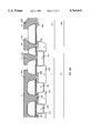
- FIG. 7 a cross sectional view of a DMOS transistor 300.
- the DMOS transistor 300 is formed on a N+ substrate 305 supporting a N epi-layer 310 thereon.
- the DMOS transistor 300 includes a plurality of cell in the core cell area each having a vertical pn-junction region with a N+ source region 315 formed on top of a deeper p-body region 320.
- the DMOS transistor 300 further includes a gate 325 formed with polysilicon layer deposited in a trench formed in the epi-layer 310. A current path is established from the source 315 via a channel formed in the p-body along the gate 325 and extend to the drain in the N+ substrate 305.
- an extra-wide termination runner 340 which is in electrical communication with the gate 325 and formed with great width including polysilicon deposited in an extra-wide trench, e.g., a trench with a width of about two to three microns.
- a PSG or BPSG insulation layer 345 is formed on top of the entire active area.
- a contact mask is then applied to open a plurality contact windows on top of the sources 315 and the p+ region 335 in the core cell area for forming the source contact 350. Contact windows are also opened in the termination area above the extra-wide termination runner 340 for forming gate contact 360.
- Clearly shown in this cross-sectional view of the DMOS transistor 300 is the elimination of gate oxide layer in the corners or edges around the trenches.
- the gate contact 360 is formed directly on top of the extra-wide termination runner 340 to assure good contact are formed and attached securely thereon. Additional advantage is provided by the use of the extra-width of the extra-wide termination runner 340. Under the circumstance that the termination runner is formed with a regular width, e.g. one-micron, due to the limitation of the etching processes in opening the gate contact window on a PSG or a BPSG layer 345, extra carefulness is required that the gate contact window is limited to the area above the gate poly only. When the etch process is not carefully performed, lateral extension of the etching can inadvertently penetrate into the p-body region 320 and create an undesirable short circuit condition.
- the terminal runner 340 By making the terminal runner 340 extra wide, in addition to the benefit that good gate contacts are formed, the concern for inadvertently forming a short circuit configuration between the gate contact 360 and the p-body 320 can be resolved. Furthermore, extra cost savings are achieved because the requirement of a poly mask is now eliminated when the poly layer above the trench over the entire area can be removed when the extra-wide termination gate runner 340 in the trench provides contact windows for making the gate contacts 380 right above the extra-wide termination gate runner 325.
- the processing steps begins by first growing a N epitaxial layer 410 with a resistivity ranging from 0.1 to 1.0 ohm-cm on top of a N+ substrate 405.
- the substrate has a resistivity of 0.001 to 0.007 ohm-cm.
- the thickness and the resistivity of the epitaxial layer 410 depend on the device requirements for the on-resistance and breakdown voltage. In a preferred embodiment, the thickness of the epi-layer 410 is about three to twenty microns (3-20 ⁇ m).
- a photoresist is employed as a trench mask
- a trench etch process which is a dry anisotropic etch process, is applied to form trenches of 1.0 to 2.0 microns wide and 1.0 to 2.0 micron in depth.
- a sacrification oxidation process is applied which can be either a dry or wet oxidation process conducted at a temperature of 900°-1100° C. to form oxide layer of approximately 300-2000 ⁇ in thickness which is followed by a sacrification oxide etch process.
- a gate oxide layer 415 is then formed by a gate oxidation process which can be a wet or dry oxidation process carried out at a temperature of 800° to 1100° C. to form a layer of thickness in the range of 200 to 1,000 ⁇ .
- a poly deposition process is performed to deposit a poly layer 420 ranging from 1.5 to 3.0 ⁇ in thickness.
- a planarization etch is performed to form a planar surface by etching a top layer to 0.2-0.5 ⁇ from the deposited poly.
- a POCL 3 doping process is carried out at 950° C. to make the poly layer 420 have a sheet resistance of 20-40 ohm/cm 2 . Referring to FIG. 8B, where a poly etch is carried out to dry etch the poly layer 420 till the top surface is removed with the end-point detection to terminate the etch process when the polysilicon layer above the trench is removed.
- a p-body mask 425 is applied to perform a p-body implant with boron ions at 30-100 Kev with an ion beam of 2 ⁇ 10 13 to 2 ⁇ 10 14 /cm 2 flux density to form the p-body region 430.
- the resist 425 is then stripped.
- a p-body diffusion process is then carried out at an elevated temperature of 1,000°-1,200° C. for ten minutes to three hours to increase the depth of the p-body region 430 to 1.0-2.0 ⁇ .
- a N+ block mask 435 is applied to carry out an N+ implant to form the N+ region 440.
- the N+ implantation is carried out with an arsenic or phosphorus ion beam at an energy of 40-100 Kev and ion flux density of 5 ⁇ 10 15 to 1 ⁇ 10 16 /cm 2 then the resist, i.e., the N+ blocking mask 435, is stripped.
- the N+ source regions 440 are driven into desired junction depth ranging from 0.2 to 1.0 ⁇ by a diffusion process at a temperature of 900°-1000° C. for 10 minutes to two hours.
- a low pressure chemical vapor deposition (LPCVD) nitride layer 438 is formed over the top surface.
- a BPSG or PSG is deposited to form a layer 445 of approximately 5000-15,000 ⁇ in thickness.
- a BPSG flow or PSG densification process is performed at 900°-950° C. for thirty minutes to one hour.
- a contact mask is applied to perform a dry etch process to define the contacts windows in order to be ready for making source and gate contacts.
- a blank boron implant with an ion beam of 20-50 Kev and ion flux of 10 15 to 1 ⁇ 10 16 /cm 2 is carried out.
- the p+ region is activated at 900°-950° C. in an oxidation or inert gas ambient.
- a metal deposition process is carried out to form an overlaying metal layer.
- the final DMOS transistor 400 is completed by applying a metal mask to pattern the source contact 450, the gate contact 460, the field plate 470 and the channel stop (CS) 480.
- FIG. 8F to 8H an extra-wide termination gate-runner 485 is formed.
- the floating ring (FR) region 488 and a channel step 480 are formed.
- the field ring FR 488 is not required because different breakdown voltage requirement.
- the field plate 470 is not required as a series of floating rings 488 and a channel are employed for another breakdown voltage requirement.
- a passivation layer is not required because the mobile ions are totally blocked by the LPCVD nitride layer 438 from entering the transistor.
- the present invention provides an improved trenched DMOS structure, and fabrication process to overcome the difficulties of the early breakdown in the gate oxide caused by the two-dimensional and three-dimensional effects over the trench edges and corners as encountered in the prior art.
- a first improved structure is provided by opening a gate window at the end of the trench stripes along the poly fingers whereby, by removing the poly layer in the gate window areas above the end of the trench stripes, the three-dimensional effects caused by the gate oxide overlaying the trench corners is eliminated and the difficulties caused by the weak points in the oxide layer over trench corners are resolved.
- a second improved structure is provided by forming a terminal gate-contact runner and by opening gate window on the terminal gate-contact runner such that the difficulties of breakdown weak points can be resolved.
- a third improved structure is provided by forming an extra-wide terminal gate-contact runner and by forming gate contact window above the extra-wide terminal gate-contact runner for gate-contacts to be formed therein such that the need for raising the gate poly above the trench is eliminated and the difficulties of breakdown weak points and poor gate contacts can be resolved. Additionally, a simplified fabrication method is disclosed, when the extra-wide gate runner is implemented, the number of masks required for manufacturing the DMOS transistors is reduced because the need of poly mask is eliminated, and thus a cost saving of manufacture is also achieved.
Abstract
Description
Claims (7)
Priority Applications (1)
| Application Number | Priority Date | Filing Date | Title |
|---|---|---|---|
| US08/607,715 US5763915A (en) | 1996-02-27 | 1996-02-27 | DMOS transistors having trenched gate oxide |
Applications Claiming Priority (1)
| Application Number | Priority Date | Filing Date | Title |
|---|---|---|---|
| US08/607,715 US5763915A (en) | 1996-02-27 | 1996-02-27 | DMOS transistors having trenched gate oxide |
Publications (1)
| Publication Number | Publication Date |
|---|---|
| US5763915A true US5763915A (en) | 1998-06-09 |
Family
ID=24433403
Family Applications (1)
| Application Number | Title | Priority Date | Filing Date |
|---|---|---|---|
| US08/607,715 Expired - Lifetime US5763915A (en) | 1996-02-27 | 1996-02-27 | DMOS transistors having trenched gate oxide |
Country Status (1)
| Country | Link |
|---|---|
| US (1) | US5763915A (en) |
Cited By (55)
| Publication number | Priority date | Publication date | Assignee | Title |
|---|---|---|---|---|
| EP1009035A1 (en) * | 1997-08-29 | 2000-06-14 | Mitsubishi Denki Kabushiki Kaisha | Insulated gate semiconductor device and method for manufacturing the same |
| WO2000042665A1 (en) * | 1999-01-11 | 2000-07-20 | Fraunhofer-Gesellschaft zur Förderung der angewandten Forschung e.V. | Power mos element and method for producing the same |
| WO2001065607A2 (en) * | 2000-02-29 | 2001-09-07 | General Semiconductor, Inc. | Trench gate dmos field-effect transistor |
| US6410959B2 (en) * | 1997-08-28 | 2002-06-25 | Hitachi, Ltd. | Method of fabricating semiconductor device |
| WO2002097876A2 (en) * | 2001-05-29 | 2002-12-05 | Koninklijke Philips Electronics N.V. | Manufacture of trench-gate field-effect transistors |
| US20030001215A1 (en) * | 2001-10-02 | 2003-01-02 | Fraunhofer-Gesellschaft Zur Foerderung Derangewandten Forschung E.V. | Power MOS element and method for producing the same |
| US20030003669A1 (en) * | 2001-06-29 | 2003-01-02 | Atmel Germany Gmbh | Process for manufacturing a DMOS transistor |
| US6521497B2 (en) * | 1997-11-14 | 2003-02-18 | Fairchild Semiconductor Corporation | Method of manufacturing a field effect transistor |
| US20030160262A1 (en) * | 2002-02-20 | 2003-08-28 | Mizue Kitada | Diode device and transistor device |
| EP1351313A2 (en) | 2002-03-22 | 2003-10-08 | Siliconix Incorporated | Structures of and methods of fabricating trench-gated MIS devices |
| US20030209757A1 (en) * | 2002-03-28 | 2003-11-13 | Ralf Henninger | Semiconductor component with an increased breakdown voltage in the edge area |
| US6780713B2 (en) | 2001-06-29 | 2004-08-24 | Atmel Germany Gmbh | Process for manufacturing a DMOS transistor |
| WO2004079794A2 (en) | 2003-03-05 | 2004-09-16 | Advanced Analogic Technologies Inc. | Trench power mosfet with planarized gate bus |
| US6806131B2 (en) * | 2001-06-29 | 2004-10-19 | Atmel Germany Gmbh | Process for manufacturing a DMOS transistor |
| US6838735B1 (en) * | 2000-02-24 | 2005-01-04 | International Rectifier Corporation | Trench FET with non overlapping poly and remote contact therefor |
| US20050062102A1 (en) * | 2003-09-19 | 2005-03-24 | Atmel Germany Gmbh | DMOS-transistor with lateral dopant gradient in drift region and method of producing the same |
| DE10350684A1 (en) * | 2003-10-30 | 2005-06-09 | Infineon Technologies Ag | Production of a power transistor arrangement used as a metal oxide semiconductor power transistor involves forming a cell field in a semiconductor substrate, inserting cell field trenches and a connecting trench within the cell field |
| US20050167749A1 (en) * | 2001-09-07 | 2005-08-04 | Power Integrations, Inc. | High-voltage vertical transistor with edge termination structure |
| US20060131645A1 (en) * | 2004-11-15 | 2006-06-22 | Sanyo Electric Co., Ltd. | Semiconductor device and manufacturing method thereof |
| US20060273390A1 (en) * | 2005-06-06 | 2006-12-07 | M-Mos Sdn. Bhd. | Gate contact and runners for high density trench MOSFET |
| DE10212149B4 (en) * | 2002-03-19 | 2007-10-04 | Infineon Technologies Ag | Transistor arrangement with shield electrode outside of an active cell array and reduced gate-drain capacitance |
| US20080017920A1 (en) * | 2006-01-05 | 2008-01-24 | Steven Sapp | Structure and method for improving shielded gate field effect transistors |
| US20080042172A1 (en) * | 2006-08-03 | 2008-02-21 | Infineon Technologies Austria Ag | Semiconductor component having a space saving edge structure |
| US20090008723A1 (en) * | 2007-07-02 | 2009-01-08 | Infineon Technologies Austria Ag | Semiconductor component including an edge termination having a trench and method for producing |
| US20090230561A1 (en) * | 2008-03-12 | 2009-09-17 | Infineon Technologies Ag | Semiconductor device |
| DE10127885B4 (en) * | 2001-06-08 | 2009-09-24 | Infineon Technologies Ag | Trench power semiconductor device |
| US20100123187A1 (en) * | 2008-11-14 | 2010-05-20 | Burke Peter A | Contact structure for semiconductor device having trench shield electrode and method |
| US20100123189A1 (en) * | 2008-11-14 | 2010-05-20 | Prasad Venkatraman | Semiconductor component and method of manufacture |
| US20100123193A1 (en) * | 2008-11-14 | 2010-05-20 | Burke Peter A | Semiconductor component and method of manufacture |
| US20100123220A1 (en) * | 2008-11-14 | 2010-05-20 | Burke Peter A | Trench shielding structure for semiconductor device and method |
| US20100123188A1 (en) * | 2008-11-14 | 2010-05-20 | Prasad Venkatraman | Semiconductor device having trench shield electrode structure |
| US20100123192A1 (en) * | 2008-11-14 | 2010-05-20 | Burke Peter A | Semiconductor component and method of manufacture |
| US20100155879A1 (en) * | 2008-03-12 | 2010-06-24 | Infineon Technologies Ag | Semiconductor device |
| US20100163950A1 (en) * | 2008-06-30 | 2010-07-01 | Jon Gladish | Power Device with Monolithically Integrated RC Snubber |
| US20100181617A1 (en) * | 2009-01-20 | 2010-07-22 | Il Kwan Lee | Method for Forming a Patterned Thick Metallization atop a Power Semiconductor Chip |
| US7772668B2 (en) * | 2007-12-26 | 2010-08-10 | Fairchild Semiconductor Corporation | Shielded gate trench FET with multiple channels |
| US20100285646A1 (en) * | 2009-05-08 | 2010-11-11 | Wei-Chieh Lin | Method of fabricating power semiconductor device |
| US20100320534A1 (en) * | 2008-06-20 | 2010-12-23 | James Pan | Structure and Method for Forming a Thick Bottom Dielectric (TBD) for Trench-Gate Devices |
| US20110136310A1 (en) * | 2009-12-09 | 2011-06-09 | Grivna Gordon M | Method of forming an insulated gate field effect transistor device having a shield electrode structure |
| US20110136309A1 (en) * | 2009-12-09 | 2011-06-09 | Grivna Gordon M | Method of forming an insulated gate field effect transistor device having a shield electrode structure |
| DE10262121B4 (en) * | 2002-03-28 | 2012-03-22 | Infineon Technologies Ag | Semiconducting component with increased breakdown voltage in edge region has shorter distance from edge cell trench to that of adjacent cell than between trenches of cells in cell field |
| CN101826551B (en) * | 2009-03-03 | 2012-12-05 | M-Mos半导体香港有限公司 | Trench type semiconductor power device with low gate resistance and preparation method thereof |
| CN104701174A (en) * | 2013-12-09 | 2015-06-10 | 上海华虹宏力半导体制造有限公司 | Optimization method for middle-pressure trench gate MOS (metal oxide semiconductor) machining technology |
| CN104733531A (en) * | 2013-12-22 | 2015-06-24 | 万国半导体股份有限公司 | Dual oxide trench gate power mosfet using oxide filled trench |
| US9252251B2 (en) | 2006-08-03 | 2016-02-02 | Infineon Technologies Austria Ag | Semiconductor component with a space saving edge structure |
| EP2903028A4 (en) * | 2013-01-15 | 2016-06-08 | Csmc Technologies Fab1 Co Ltd | Trench dmos device and manufacturing method thereof |
| US9425305B2 (en) | 2009-10-20 | 2016-08-23 | Vishay-Siliconix | Structures of and methods of fabricating split gate MIS devices |
| US9577089B2 (en) | 2010-03-02 | 2017-02-21 | Vishay-Siliconix | Structures and methods of fabricating dual gate devices |
| JP2018074126A (en) * | 2016-11-04 | 2018-05-10 | トヨタ自動車株式会社 | Semiconductor device |
| US10438813B2 (en) | 2017-11-13 | 2019-10-08 | Alpha And Omega Semiconductor (Cayman) Ltd. | Semiconductor device having one or more titanium interlayers and method of making the same |
| DE10261464B4 (en) | 2002-03-07 | 2021-08-12 | Mitsubishi Denki K.K. | Isolated gate semiconductor device having a trench structure |
| US11114559B2 (en) | 2011-05-18 | 2021-09-07 | Vishay-Siliconix, LLC | Semiconductor device having reduced gate charges and superior figure of merit |
| US11218144B2 (en) | 2019-09-12 | 2022-01-04 | Vishay-Siliconix, LLC | Semiconductor device with multiple independent gates |
| US11217541B2 (en) | 2019-05-08 | 2022-01-04 | Vishay-Siliconix, LLC | Transistors with electrically active chip seal ring and methods of manufacture |
| US20220262909A1 (en) * | 2021-02-17 | 2022-08-18 | Cree, Inc. | Power semiconductor device with reduced strain |
Citations (2)
| Publication number | Priority date | Publication date | Assignee | Title |
|---|---|---|---|---|
| US4547791A (en) * | 1981-04-29 | 1985-10-15 | U.S. Philips Corporation | CMOS-Bipolar Darlington device |
| US5541425A (en) * | 1994-01-20 | 1996-07-30 | Mitsubishi Denki Kabushiki Kaisha | Semiconductor device having trench structure |
-
1996
- 1996-02-27 US US08/607,715 patent/US5763915A/en not_active Expired - Lifetime
Patent Citations (2)
| Publication number | Priority date | Publication date | Assignee | Title |
|---|---|---|---|---|
| US4547791A (en) * | 1981-04-29 | 1985-10-15 | U.S. Philips Corporation | CMOS-Bipolar Darlington device |
| US5541425A (en) * | 1994-01-20 | 1996-07-30 | Mitsubishi Denki Kabushiki Kaisha | Semiconductor device having trench structure |
Cited By (150)
| Publication number | Priority date | Publication date | Assignee | Title |
|---|---|---|---|---|
| US9275863B2 (en) | 1997-08-28 | 2016-03-01 | Renesas Electronics Corporation | Method of fabricating semiconductor device |
| US20070290239A1 (en) * | 1997-08-28 | 2007-12-20 | Sumito Numazawa | Method of fabricating semiconductor device |
| US6720220B2 (en) | 1997-08-28 | 2004-04-13 | Renesas Technology Corp. | Method of fabricating semiconductor device |
| US8076202B2 (en) | 1997-08-28 | 2011-12-13 | Renesas Electronics Corporation | Method of fabricating semiconductor device |
| US6410959B2 (en) * | 1997-08-28 | 2002-06-25 | Hitachi, Ltd. | Method of fabricating semiconductor device |
| US7180130B2 (en) | 1997-08-28 | 2007-02-20 | Renesas Technology Corp. | Method of fabricating semiconductor device |
| US20050037579A1 (en) * | 1997-08-28 | 2005-02-17 | Renesas Technology Corp. | Method of fabricating semiconductor device |
| US6803281B2 (en) | 1997-08-28 | 2004-10-12 | Renesas Technology Corp. | Method of fabricating semiconductor device |
| US20110215398A1 (en) * | 1997-08-28 | 2011-09-08 | Renesas Electronics Corporation | Method of fabricating semiconductor device |
| US8354713B2 (en) | 1997-08-28 | 2013-01-15 | Renesas Electronics Corporation | Method of fabricating semiconductor device |
| US20040166656A1 (en) * | 1997-08-28 | 2004-08-26 | Renesas Technology Corp. | Method of fabricating semiconductor device |
| US6512265B2 (en) * | 1997-08-28 | 2003-01-28 | Hitachi, Ltd. | Method of fabricating semiconductor device |
| US20070290268A1 (en) * | 1997-08-28 | 2007-12-20 | Sumito Numazawa | Method of fabricating semiconductor device |
| US8748266B2 (en) | 1997-08-28 | 2014-06-10 | Renesas Electronics Corporation | Method of fabricating semiconductor device |
| US20070278567A1 (en) * | 1997-08-28 | 2007-12-06 | Sumito Numazawa | Method of fabricating semiconductor device |
| US20070111423A1 (en) * | 1997-08-28 | 2007-05-17 | Sumito Numazawa | Method of fabricating semiconductor device |
| US20100173461A1 (en) * | 1997-08-28 | 2010-07-08 | Renesas Technology Corp. | Method of fabricating semiconductor device |
| EP1009035A1 (en) * | 1997-08-29 | 2000-06-14 | Mitsubishi Denki Kabushiki Kaisha | Insulated gate semiconductor device and method for manufacturing the same |
| EP1009035A4 (en) * | 1997-08-29 | 2003-01-08 | Mitsubishi Electric Corp | Insulated gate semiconductor device and method for manufacturing the same |
| US7696571B2 (en) | 1997-11-14 | 2010-04-13 | Fairchild Semiconductor Corporation | Method of manufacturing a trench transistor having a heavy body region |
| US20100264487A1 (en) * | 1997-11-14 | 2010-10-21 | Brian Sze-Ki Mo | Method of Manufacturing a Trench Transistor Having a Heavy Body Region |
| US20040145015A1 (en) * | 1997-11-14 | 2004-07-29 | Fairchild Semiconductor Corporation | Field effect transistor and method of its manufacture |
| US7736978B2 (en) | 1997-11-14 | 2010-06-15 | Fairchild Semiconductor Corporation | Method of manufacturing a trench transistor having a heavy body region |
| US6521497B2 (en) * | 1997-11-14 | 2003-02-18 | Fairchild Semiconductor Corporation | Method of manufacturing a field effect transistor |
| US7148111B2 (en) | 1997-11-14 | 2006-12-12 | Fairchild Semiconductor Corporation | Method of manufacturing a trench transistor having a heavy body region |
| US20090134458A1 (en) * | 1997-11-14 | 2009-05-28 | Brian Sze-Ki Mo | Method of Manufacturing a Trench Transistor Having a Heavy Body Region |
| US20070042551A1 (en) * | 1997-11-14 | 2007-02-22 | Mo Brian S | Method of manufacturing a trench transistor having a heavy body region |
| US20100112767A1 (en) * | 1997-11-14 | 2010-05-06 | Brian Sze-Ki Mo | Method of Manufacturing a Trench Transistor Having a Heavy Body Region |
| US6828195B2 (en) | 1997-11-14 | 2004-12-07 | Fairchild Semiconductor Corporation | Method of manufacturing a trench transistor having a heavy body region |
| US8044463B2 (en) | 1997-11-14 | 2011-10-25 | Fairchild Semiconductor Corporation | Method of manufacturing a trench transistor having a heavy body region |
| US8476133B2 (en) | 1997-11-14 | 2013-07-02 | Fairchild Semiconductor Corporation | Method of manufacture and structure for a trench transistor having a heavy body region |
| US7511339B2 (en) | 1997-11-14 | 2009-03-31 | Fairchild Semiconductor Corporation | Field effect transistor and method of its manufacture |
| US20050079676A1 (en) * | 1997-11-14 | 2005-04-14 | Fairchild Semiconductor Corporation | Method of manufacturing a trench transistor having a heavy body region |
| WO2000042665A1 (en) * | 1999-01-11 | 2000-07-20 | Fraunhofer-Gesellschaft zur Förderung der angewandten Forschung e.V. | Power mos element and method for producing the same |
| US6462376B1 (en) | 1999-01-11 | 2002-10-08 | Fraunhofer-Gesellschaft Zur Foerderung Der Angewandten Forschung E.V. | Power MOS element and method for producing the same |
| US6838735B1 (en) * | 2000-02-24 | 2005-01-04 | International Rectifier Corporation | Trench FET with non overlapping poly and remote contact therefor |
| WO2001065607A2 (en) * | 2000-02-29 | 2001-09-07 | General Semiconductor, Inc. | Trench gate dmos field-effect transistor |
| WO2001065607A3 (en) * | 2000-02-29 | 2002-05-30 | Gen Semiconductor Inc | Trench gate dmos field-effect transistor |
| EP2267786A3 (en) * | 2000-02-29 | 2011-01-12 | GENERAL SEMICONDUCTOR, Inc. | Trench gate DMOS field-effect transistor |
| US6548860B1 (en) | 2000-02-29 | 2003-04-15 | General Semiconductor, Inc. | DMOS transistor structure having improved performance |
| JP2003529209A (en) * | 2000-02-29 | 2003-09-30 | ゼネラル セミコンダクター,インク. | Trench double diffused metal oxide semiconductor transistor structure |
| WO2002097876A3 (en) * | 2001-05-29 | 2003-05-01 | Koninkl Philips Electronics Nv | Manufacture of trench-gate field-effect transistors |
| WO2002097876A2 (en) * | 2001-05-29 | 2002-12-05 | Koninklijke Philips Electronics N.V. | Manufacture of trench-gate field-effect transistors |
| DE10127885B4 (en) * | 2001-06-08 | 2009-09-24 | Infineon Technologies Ag | Trench power semiconductor device |
| US6806131B2 (en) * | 2001-06-29 | 2004-10-19 | Atmel Germany Gmbh | Process for manufacturing a DMOS transistor |
| US20030003669A1 (en) * | 2001-06-29 | 2003-01-02 | Atmel Germany Gmbh | Process for manufacturing a DMOS transistor |
| US6780713B2 (en) | 2001-06-29 | 2004-08-24 | Atmel Germany Gmbh | Process for manufacturing a DMOS transistor |
| US6878603B2 (en) * | 2001-06-29 | 2005-04-12 | Atmel Germany Gmbh | Process for manufacturing a DMOS transistor |
| US7786533B2 (en) * | 2001-09-07 | 2010-08-31 | Power Integrations, Inc. | High-voltage vertical transistor with edge termination structure |
| US8552496B2 (en) * | 2001-09-07 | 2013-10-08 | Power Integrations, Inc. | High-voltage vertical transistor with edge termination structure |
| US20110018058A1 (en) * | 2001-09-07 | 2011-01-27 | Power Integrations, Inc. | High-voltage vertical transistor with edge termination structure |
| US20050167749A1 (en) * | 2001-09-07 | 2005-08-04 | Power Integrations, Inc. | High-voltage vertical transistor with edge termination structure |
| US6693011B2 (en) * | 2001-10-02 | 2004-02-17 | Fraunhofer-Gesellschaft Zur Foerderung Der Angewandten Forschung E.V. | Power MOS element and method for producing the same |
| US20030001215A1 (en) * | 2001-10-02 | 2003-01-02 | Fraunhofer-Gesellschaft Zur Foerderung Derangewandten Forschung E.V. | Power MOS element and method for producing the same |
| US20030160262A1 (en) * | 2002-02-20 | 2003-08-28 | Mizue Kitada | Diode device and transistor device |
| US7135718B2 (en) * | 2002-02-20 | 2006-11-14 | Shindengen Electric Manufacturing Co., Ltd. | Diode device and transistor device |
| DE10261464B4 (en) | 2002-03-07 | 2021-08-12 | Mitsubishi Denki K.K. | Isolated gate semiconductor device having a trench structure |
| DE10212149B4 (en) * | 2002-03-19 | 2007-10-04 | Infineon Technologies Ag | Transistor arrangement with shield electrode outside of an active cell array and reduced gate-drain capacitance |
| JP2003309263A (en) | 2002-03-22 | 2003-10-31 | Siliconix Inc | Structure of trench gate mis device and its manufacturing method |
| CN101980356B (en) * | 2002-03-22 | 2013-04-03 | 西利康尼克斯股份有限公司 | Structures of and methods of fabricating trench-gated mis devices |
| US7335946B1 (en) | 2002-03-22 | 2008-02-26 | Vishay-Siliconix | Structures of and methods of fabricating trench-gated MIS devices |
| JP2012060147A (en) * | 2002-03-22 | 2012-03-22 | Siliconix Inc | Structure of trench-gate mis device and method of manufacturing the same |
| US20110042742A1 (en) * | 2002-03-22 | 2011-02-24 | Vishay-Siliconix | Structures of and methods of fabricating trench-gated mis devices |
| EP1351313A2 (en) | 2002-03-22 | 2003-10-08 | Siliconix Incorporated | Structures of and methods of fabricating trench-gated MIS devices |
| EP1351313A3 (en) * | 2002-03-22 | 2007-12-26 | Siliconix Incorporated | Structures of and methods of fabricating trench-gated MIS devices |
| CN100433366C (en) * | 2002-03-22 | 2008-11-12 | 西利康尼克斯股份有限公司 | Structure of groove-grid MIS device and producing method thereof |
| US9324858B2 (en) | 2002-03-22 | 2016-04-26 | Vishay-Siliconix | Trench-gated MIS devices |
| US6838722B2 (en) | 2002-03-22 | 2005-01-04 | Siliconix Incorporated | Structures of and methods of fabricating trench-gated MIS devices |
| US7868381B1 (en) | 2002-03-22 | 2011-01-11 | Vishay-Siliconix | Structures of and methods of fabricating trench-gated MIS devices |
| US6806533B2 (en) * | 2002-03-28 | 2004-10-19 | Infineon Technologies Ag | Semiconductor component with an increased breakdown voltage in the edge area |
| US20030209757A1 (en) * | 2002-03-28 | 2003-11-13 | Ralf Henninger | Semiconductor component with an increased breakdown voltage in the edge area |
| DE10262121B4 (en) * | 2002-03-28 | 2012-03-22 | Infineon Technologies Ag | Semiconducting component with increased breakdown voltage in edge region has shorter distance from edge cell trench to that of adjacent cell than between trenches of cells in cell field |
| EP1599907A2 (en) * | 2003-03-05 | 2005-11-30 | Advanced Analogic Technologies, Inc. | Trench power mosfet with planarized gate bus |
| EP1599907A4 (en) * | 2003-03-05 | 2010-07-07 | Advanced Analogic Tech Inc | Trench power mosfet with planarized gate bus |
| WO2004079794A2 (en) | 2003-03-05 | 2004-09-16 | Advanced Analogic Technologies Inc. | Trench power mosfet with planarized gate bus |
| US7064385B2 (en) | 2003-09-19 | 2006-06-20 | Atmel Germany Gmbh | DMOS-transistor with lateral dopant gradient in drift region and method of producing the same |
| US20050062102A1 (en) * | 2003-09-19 | 2005-03-24 | Atmel Germany Gmbh | DMOS-transistor with lateral dopant gradient in drift region and method of producing the same |
| DE10350684A1 (en) * | 2003-10-30 | 2005-06-09 | Infineon Technologies Ag | Production of a power transistor arrangement used as a metal oxide semiconductor power transistor involves forming a cell field in a semiconductor substrate, inserting cell field trenches and a connecting trench within the cell field |
| DE10350684B4 (en) * | 2003-10-30 | 2008-08-28 | Infineon Technologies Ag | Method for producing a power transistor arrangement and power transistor arrangement produced by this method |
| US7186618B2 (en) | 2003-10-30 | 2007-03-06 | Infineon Technologies Ag | Power transistor arrangement and method for fabricating it |
| US20050145936A1 (en) * | 2003-10-30 | 2005-07-07 | Infineon Technologies Ag | Power transistor arrangement and method for fabricating it |
| US20060131645A1 (en) * | 2004-11-15 | 2006-06-22 | Sanyo Electric Co., Ltd. | Semiconductor device and manufacturing method thereof |
| US20060273390A1 (en) * | 2005-06-06 | 2006-12-07 | M-Mos Sdn. Bhd. | Gate contact and runners for high density trench MOSFET |
| US7768064B2 (en) | 2006-01-05 | 2010-08-03 | Fairchild Semiconductor Corporation | Structure and method for improving shielded gate field effect transistors |
| US20080017920A1 (en) * | 2006-01-05 | 2008-01-24 | Steven Sapp | Structure and method for improving shielded gate field effect transistors |
| US20110163732A1 (en) * | 2006-01-05 | 2011-07-07 | Steven Sapp | Synchronous buck converter using shielded gate field effect transistors |
| US8193570B2 (en) | 2006-01-05 | 2012-06-05 | Fairchild Semiconductor Corporation | Synchronous buck converter using shielded gate field effect transistors |
| US8080858B2 (en) | 2006-08-03 | 2011-12-20 | Infineon Technologies Austria Ag | Semiconductor component having a space saving edge structure |
| US20080042172A1 (en) * | 2006-08-03 | 2008-02-21 | Infineon Technologies Austria Ag | Semiconductor component having a space saving edge structure |
| US9627520B2 (en) | 2006-08-03 | 2017-04-18 | Infineon Technologies Austria Ag | MOS transistor having a cell array edge zone arranged partially below and having an interface with a trench in an edge region of the cell array |
| US9252251B2 (en) | 2006-08-03 | 2016-02-02 | Infineon Technologies Austria Ag | Semiconductor component with a space saving edge structure |
| US8093676B2 (en) | 2007-07-02 | 2012-01-10 | Infineon Technologies Austria Ag | Semiconductor component including an edge termination having a trench and method for producing |
| US20090008723A1 (en) * | 2007-07-02 | 2009-01-08 | Infineon Technologies Austria Ag | Semiconductor component including an edge termination having a trench and method for producing |
| DE102007030755B3 (en) * | 2007-07-02 | 2009-02-19 | Infineon Technologies Austria Ag | Semiconductor device having a trench edge having edge and method for producing a border termination |
| US9224853B2 (en) | 2007-12-26 | 2015-12-29 | Fairchild Semiconductor Corporation | Shielded gate trench FET with multiple channels |
| US7772668B2 (en) * | 2007-12-26 | 2010-08-10 | Fairchild Semiconductor Corporation | Shielded gate trench FET with multiple channels |
| US8866255B2 (en) | 2008-03-12 | 2014-10-21 | Infineon Technologies Austria Ag | Semiconductor device with staggered oxide-filled trenches at edge region |
| US9508812B2 (en) | 2008-03-12 | 2016-11-29 | Infineon Technologies Austria Ag | Semiconductor device |
| US9287373B2 (en) | 2008-03-12 | 2016-03-15 | Infineon Technologies Ag | Semiconductor device |
| US20090230561A1 (en) * | 2008-03-12 | 2009-09-17 | Infineon Technologies Ag | Semiconductor device |
| US8809966B2 (en) * | 2008-03-12 | 2014-08-19 | Infineon Technologies Ag | Semiconductor device |
| US20100155879A1 (en) * | 2008-03-12 | 2010-06-24 | Infineon Technologies Ag | Semiconductor device |
| US20100320534A1 (en) * | 2008-06-20 | 2010-12-23 | James Pan | Structure and Method for Forming a Thick Bottom Dielectric (TBD) for Trench-Gate Devices |
| US8669623B2 (en) | 2008-06-20 | 2014-03-11 | Fairchild Semiconductor Corporation | Structure related to a thick bottom dielectric (TBD) for trench-gate devices |
| US20100163950A1 (en) * | 2008-06-30 | 2010-07-01 | Jon Gladish | Power Device with Monolithically Integrated RC Snubber |
| US8829624B2 (en) | 2008-06-30 | 2014-09-09 | Fairchild Semiconductor Corporation | Power device with monolithically integrated RC snubber |
| US9306018B2 (en) | 2008-11-14 | 2016-04-05 | Semiconductor Components Industries, Llc | Trench shielding structure for semiconductor device and method |
| US7915672B2 (en) | 2008-11-14 | 2011-03-29 | Semiconductor Components Industries, L.L.C. | Semiconductor device having trench shield electrode structure |
| US20100123187A1 (en) * | 2008-11-14 | 2010-05-20 | Burke Peter A | Contact structure for semiconductor device having trench shield electrode and method |
| US8362548B2 (en) | 2008-11-14 | 2013-01-29 | Semiconductor Components Industries, Llc | Contact structure for semiconductor device having trench shield electrode and method |
| US20100123192A1 (en) * | 2008-11-14 | 2010-05-20 | Burke Peter A | Semiconductor component and method of manufacture |
| US8415739B2 (en) | 2008-11-14 | 2013-04-09 | Semiconductor Components Industries, Llc | Semiconductor component and method of manufacture |
| US20100123193A1 (en) * | 2008-11-14 | 2010-05-20 | Burke Peter A | Semiconductor component and method of manufacture |
| US8552535B2 (en) | 2008-11-14 | 2013-10-08 | Semiconductor Components Industries, Llc | Trench shielding structure for semiconductor device and method |
| US20100123220A1 (en) * | 2008-11-14 | 2010-05-20 | Burke Peter A | Trench shielding structure for semiconductor device and method |
| US7897462B2 (en) | 2008-11-14 | 2011-03-01 | Semiconductor Components Industries, L.L.C. | Method of manufacturing semiconductor component with gate and shield electrodes in trenches |
| US20100123188A1 (en) * | 2008-11-14 | 2010-05-20 | Prasad Venkatraman | Semiconductor device having trench shield electrode structure |
| US20100123189A1 (en) * | 2008-11-14 | 2010-05-20 | Prasad Venkatraman | Semiconductor component and method of manufacture |
| US8354334B2 (en) * | 2009-01-20 | 2013-01-15 | Alpha & Omega Semiconductor Inc. | Power semiconductor chip with a formed patterned thick metallization atop |
| US20100181617A1 (en) * | 2009-01-20 | 2010-07-22 | Il Kwan Lee | Method for Forming a Patterned Thick Metallization atop a Power Semiconductor Chip |
| US8067304B2 (en) * | 2009-01-20 | 2011-11-29 | Alpha And Omega Semiconductor, Inc. | Method for forming a patterned thick metallization atop a power semiconductor chip |
| US20120037981A1 (en) * | 2009-01-20 | 2012-02-16 | Il Kwan Lee | Power Semiconductor Chip with a Formed Patterned Thick Metallization Atop |
| CN101826551B (en) * | 2009-03-03 | 2012-12-05 | M-Mos半导体香港有限公司 | Trench type semiconductor power device with low gate resistance and preparation method thereof |
| US20100285646A1 (en) * | 2009-05-08 | 2010-11-11 | Wei-Chieh Lin | Method of fabricating power semiconductor device |
| US7867854B2 (en) | 2009-05-08 | 2011-01-11 | Anpec Electronics Corporation | Method of fabricating power semiconductor device |
| US9425305B2 (en) | 2009-10-20 | 2016-08-23 | Vishay-Siliconix | Structures of and methods of fabricating split gate MIS devices |
| US20110136309A1 (en) * | 2009-12-09 | 2011-06-09 | Grivna Gordon M | Method of forming an insulated gate field effect transistor device having a shield electrode structure |
| US20110136310A1 (en) * | 2009-12-09 | 2011-06-09 | Grivna Gordon M | Method of forming an insulated gate field effect transistor device having a shield electrode structure |
| US8247296B2 (en) | 2009-12-09 | 2012-08-21 | Semiconductor Components Industries, Llc | Method of forming an insulated gate field effect transistor device having a shield electrode structure |
| US8664065B2 (en) | 2009-12-09 | 2014-03-04 | Semiconductor Components Industries, Llc | Method of forming an insulated gate field effect transistor device having a shield electrode structure |
| US8021947B2 (en) | 2009-12-09 | 2011-09-20 | Semiconductor Components Industries, Llc | Method of forming an insulated gate field effect transistor device having a shield electrode structure |
| US10453953B2 (en) | 2010-03-02 | 2019-10-22 | Vishay-Siliconix | Structures and methods of fabricating dual gate devices |
| US9577089B2 (en) | 2010-03-02 | 2017-02-21 | Vishay-Siliconix | Structures and methods of fabricating dual gate devices |
| US11114559B2 (en) | 2011-05-18 | 2021-09-07 | Vishay-Siliconix, LLC | Semiconductor device having reduced gate charges and superior figure of merit |
| EP2903028A4 (en) * | 2013-01-15 | 2016-06-08 | Csmc Technologies Fab1 Co Ltd | Trench dmos device and manufacturing method thereof |
| CN104701174A (en) * | 2013-12-09 | 2015-06-10 | 上海华虹宏力半导体制造有限公司 | Optimization method for middle-pressure trench gate MOS (metal oxide semiconductor) machining technology |
| CN104701174B (en) * | 2013-12-09 | 2017-12-05 | 上海华虹宏力半导体制造有限公司 | Method for pressing trench grate MOS processing technology in optimization |
| US20150179750A1 (en) * | 2013-12-22 | 2015-06-25 | Alpha And Omega Semiconductor Incorporated | Dual oxide trench gate power mosfet using oxide filled trench |
| US9190478B2 (en) * | 2013-12-22 | 2015-11-17 | Alpha And Omega Semiconductor Incorporated | Method for forming dual oxide trench gate power MOSFET using oxide filled trench |
| CN104733531B (en) * | 2013-12-22 | 2018-04-03 | 万国半导体股份有限公司 | Use the double oxide Trench-gate power MOSFET of oxide filling groove |
| CN104733531A (en) * | 2013-12-22 | 2015-06-24 | 万国半导体股份有限公司 | Dual oxide trench gate power mosfet using oxide filled trench |
| JP2018074126A (en) * | 2016-11-04 | 2018-05-10 | トヨタ自動車株式会社 | Semiconductor device |
| WO2018083526A1 (en) * | 2016-11-04 | 2018-05-11 | Toyota Jidosha Kabushiki Kaisha | Semiconductor device |
| CN109891594A (en) * | 2016-11-04 | 2019-06-14 | 丰田自动车株式会社 | Semiconductor devices |
| US10770580B2 (en) * | 2016-11-04 | 2020-09-08 | Toyota Jidosha Kabushiki Kaisha | Semiconductor device |
| US10438813B2 (en) | 2017-11-13 | 2019-10-08 | Alpha And Omega Semiconductor (Cayman) Ltd. | Semiconductor device having one or more titanium interlayers and method of making the same |
| US11217541B2 (en) | 2019-05-08 | 2022-01-04 | Vishay-Siliconix, LLC | Transistors with electrically active chip seal ring and methods of manufacture |
| US11218144B2 (en) | 2019-09-12 | 2022-01-04 | Vishay-Siliconix, LLC | Semiconductor device with multiple independent gates |
| US20220262909A1 (en) * | 2021-02-17 | 2022-08-18 | Cree, Inc. | Power semiconductor device with reduced strain |
| US11869948B2 (en) * | 2021-02-17 | 2024-01-09 | Wolfspeed, Inc. | Power semiconductor device with reduced strain |
Similar Documents
| Publication | Publication Date | Title |
|---|---|---|
| US5763915A (en) | DMOS transistors having trenched gate oxide | |
| US6031265A (en) | Enhancing DMOS device ruggedness by reducing transistor parasitic resistance and by inducing breakdown near gate runners and termination area | |
| US6534367B2 (en) | Trench-gate semiconductor devices and their manufacture | |
| US5877528A (en) | Structure to provide effective channel-stop in termination areas for trenched power transistors | |
| US6281547B1 (en) | Power transistor cells provided with reliable trenched source contacts connected to narrower source manufactured without a source mask | |
| US9806175B2 (en) | Power MOSFET device structure for high frequency applications | |
| JP2893554B2 (en) | Trench DMOS transistor having channel blocking means at corners of cell trench | |
| US6498071B2 (en) | Manufacture of trench-gate semiconductor devices | |
| US5430324A (en) | High voltage transistor having edge termination utilizing trench technology | |
| US7005347B1 (en) | Structures of and methods of fabricating trench-gated MIS devices | |
| US5986304A (en) | Punch-through prevention in trenched DMOS with poly-silicon layer covering trench corners | |
| US6660591B2 (en) | Trench-gate semiconductor devices having a channel-accommodating region and their methods of manufacture | |
| US5668026A (en) | DMOS fabrication process implemented with reduced number of masks | |
| US20010003367A1 (en) | Trenched dmos device with low gate charges | |
| US6404025B1 (en) | MOSFET power device manufactured with reduced number of masks by fabrication simplified processes | |
| US6048759A (en) | Gate/drain capacitance reduction for double gate-oxide DMOS without degrading avalanche breakdown | |
| US6087224A (en) | Manufacture of trench-gate semiconductor devices | |
| US6104060A (en) | Cost savings for manufacturing planar MOSFET devices achieved by implementing an improved device structure and fabrication process eliminating passivation layer and/or field plate | |
| US5763914A (en) | Cell topology for power transistors with increased packing density | |
| US20020140042A1 (en) | Ultra low QGD power MOSFET | |
| WO2001069685A2 (en) | Trench-gate semiconductor devices | |
| US6228698B1 (en) | Manufacture of field-effect semiconductor devices | |
| KR20040002411A (en) | Trench-gate semiconductor devices and their manufacture | |
| JP2001508595A (en) | Fabrication of high-density trench DMOS using sidewall spacers |
Legal Events
| Date | Code | Title | Description |
|---|---|---|---|
| AS | Assignment |
Owner name: MEGAMOS CORPORATION, CALIFORNIA Free format text: ASSIGNMENT OF ASSIGNORS INTEREST;ASSIGNORS:HSHIEH, FWU-IUAN;LIN, TRUE-LON;NIM, DANNY CHI;AND OTHERS;REEL/FRAME:007889/0370;SIGNING DATES FROM 19960220 TO 19960221 |
|
| STCF | Information on status: patent grant |
Free format text: PATENTED CASE |
|
| REMI | Maintenance fee reminder mailed | ||
| FPAY | Fee payment |
Year of fee payment: 4 |
|
| SULP | Surcharge for late payment | ||
| FEPP | Fee payment procedure |
Free format text: PAYOR NUMBER ASSIGNED (ORIGINAL EVENT CODE: ASPN); ENTITY STATUS OF PATENT OWNER: LARGE ENTITY |
|
| AS | Assignment |
Owner name: SILICON SERVICES CONSORTIUM, INC., TEXAS Free format text: BILL OF SALE OF INTELLECTUAL PROPERTY;ASSIGNOR:MAGEPOWER CORPORATION FORMERLY MEGAMOS CORPORATION;REEL/FRAME:016153/0341 Effective date: 20000118 |
|
| AS | Assignment |
Owner name: CERLAN TECHNOLOGY VENTURES, LLC, CALIFORNIA Free format text: ASSIGNMENT OF ASSIGNORS INTEREST;ASSIGNOR:SILICON SERVICE CONSORTIUM, INC.;REEL/FRAME:016004/0193 Effective date: 20050127 Owner name: ALPHA AND OMEGA SEMICONDUCTOR, LTD., BERMUDA Free format text: ASSIGNMENT OF ASSIGNORS INTEREST;ASSIGNOR:CERIAN TECHNOLOGY VENTURES, LLC;REEL/FRAME:016004/0215 Effective date: 20050126 |
|
| AS | Assignment |
Owner name: ALPHA AND OMEGA SEMICONDUCTOR, LTD., BERMUDA Free format text: ASSIGNMENT OF ASSIGNORS INTEREST;ASSIGNOR:CERIAN TECHNOLOGY VENTURES, LLC;REEL/FRAME:016580/0956 Effective date: 20050603 |
|
| FPAY | Fee payment |
Year of fee payment: 8 |
|
| FEPP | Fee payment procedure |
Free format text: PAT HOLDER NO LONGER CLAIMS SMALL ENTITY STATUS, ENTITY STATUS SET TO UNDISCOUNTED (ORIGINAL EVENT CODE: STOL); ENTITY STATUS OF PATENT OWNER: LARGE ENTITY |
|
| FEPP | Fee payment procedure |
Free format text: ENTITY STATUS SET TO UNDISCOUNTED (ORIGINAL EVENT CODE: BIG.); ENTITY STATUS OF PATENT OWNER: LARGE ENTITY |
|
| FPAY | Fee payment |
Year of fee payment: 12 |
|
| SULP | Surcharge for late payment |
Year of fee payment: 11 |