US5768456A - Optoelectronic package including photonic device mounted in flexible substrate - Google Patents
Optoelectronic package including photonic device mounted in flexible substrate Download PDFInfo
- Publication number
- US5768456A US5768456A US08/753,311 US75331196A US5768456A US 5768456 A US5768456 A US 5768456A US 75331196 A US75331196 A US 75331196A US 5768456 A US5768456 A US 5768456A
- Authority
- US
- United States
- Prior art keywords
- optical fiber
- optical
- photonic
- flexible substrate
- fiber holder
- Prior art date
- Legal status (The legal status is an assumption and is not a legal conclusion. Google has not performed a legal analysis and makes no representation as to the accuracy of the status listed.)
- Expired - Fee Related
Links
Images


Classifications
-
- G—PHYSICS
- G02—OPTICS
- G02B—OPTICAL ELEMENTS, SYSTEMS OR APPARATUS
- G02B6/00—Light guides; Structural details of arrangements comprising light guides and other optical elements, e.g. couplings
- G02B6/24—Coupling light guides
- G02B6/42—Coupling light guides with opto-electronic elements
- G02B6/4292—Coupling light guides with opto-electronic elements the light guide being disconnectable from the opto-electronic element, e.g. mutually self aligning arrangements
-
- G—PHYSICS
- G02—OPTICS
- G02B—OPTICAL ELEMENTS, SYSTEMS OR APPARATUS
- G02B6/00—Light guides; Structural details of arrangements comprising light guides and other optical elements, e.g. couplings
- G02B6/24—Coupling light guides
- G02B6/42—Coupling light guides with opto-electronic elements
- G02B6/4201—Packages, e.g. shape, construction, internal or external details
- G02B6/4219—Mechanical fixtures for holding or positioning the elements relative to each other in the couplings; Alignment methods for the elements, e.g. measuring or observing methods especially used therefor
- G02B6/4236—Fixing or mounting methods of the aligned elements
- G02B6/424—Mounting of the optical light guide
-
- G—PHYSICS
- G02—OPTICS
- G02B—OPTICAL ELEMENTS, SYSTEMS OR APPARATUS
- G02B6/00—Light guides; Structural details of arrangements comprising light guides and other optical elements, e.g. couplings
- G02B6/24—Coupling light guides
- G02B6/42—Coupling light guides with opto-electronic elements
- G02B6/4201—Packages, e.g. shape, construction, internal or external details
- G02B6/4249—Packages, e.g. shape, construction, internal or external details comprising arrays of active devices and fibres
-
- G—PHYSICS
- G02—OPTICS
- G02B—OPTICAL ELEMENTS, SYSTEMS OR APPARATUS
- G02B6/00—Light guides; Structural details of arrangements comprising light guides and other optical elements, e.g. couplings
- G02B6/24—Coupling light guides
- G02B6/42—Coupling light guides with opto-electronic elements
- G02B6/4201—Packages, e.g. shape, construction, internal or external details
- G02B6/4256—Details of housings
- G02B6/4257—Details of housings having a supporting carrier or a mounting substrate or a mounting plate
-
- G—PHYSICS
- G02—OPTICS
- G02B—OPTICAL ELEMENTS, SYSTEMS OR APPARATUS
- G02B6/00—Light guides; Structural details of arrangements comprising light guides and other optical elements, e.g. couplings
- G02B6/24—Coupling light guides
- G02B6/42—Coupling light guides with opto-electronic elements
- G02B6/4201—Packages, e.g. shape, construction, internal or external details
- G02B6/4274—Electrical aspects
-
- G—PHYSICS
- G02—OPTICS
- G02B—OPTICAL ELEMENTS, SYSTEMS OR APPARATUS
- G02B6/00—Light guides; Structural details of arrangements comprising light guides and other optical elements, e.g. couplings
- G02B6/24—Coupling light guides
- G02B6/42—Coupling light guides with opto-electronic elements
- G02B6/4201—Packages, e.g. shape, construction, internal or external details
- G02B6/4256—Details of housings
- G02B6/426—Details of housings mounting, engaging or coupling of the package to a board, a frame or a panel
- G02B6/4261—Packages with mounting structures to be pluggable or detachable, e.g. having latches or rails
Definitions
- This invention relates, in general, to fabrication of optical devices and, more particularly, to interconnecting optical devices and optical fibers.
- conventional interconnection of an optical device to an optical fiber is by way of a waveguide.
- the optical fibers are carried by a connector, such as an MT connector, which is attached to one end of the waveguide with the optical fibers in alignment with the core region of the waveguide.
- Alignment of the optical device with the optical fibers is achieved by carefully aligning the optical device to the waveguide manually, commonly referred to as active alignment. Once the optical device is appropriately aligned, it is affixed to the waveguide generally by use of an adhesive.
- shifts in the alignment of the optical device to the waveguide often occur during curing of the adhesive used to affix or bind the optical device to the waveguide.
- the shift in alignment can cause inefficient transfer of light from the optical device.
- misalignment is severe enough, unusable product is manufactured, thus increasing cost and reducing manufacturing capability.
- the optical device and the waveguide are then mounted onto a substrate.
- Mounting the optical device and the waveguide to the substrate also has several problems, such as fragility of the fixed optical device and waveguide, alignment capability of the optical device and waveguide to the substrate, electrical coupling of the optical device, and the like, thus making the interconnection of the optical device, the waveguide, and the interconnect substrate unsuitable for high volume manufacturing.
- an optoelectronic mount for interconnecting fiber optics with electronic components including a flexible substrate having electrical traces extending from a first end to a second end. Alignment openings are formed in the flexible substrate proximate the first end.
- An optical fiber holder contains an end of an optical fiber and includes an end surface in which is formed alignment openings, the optical fiber has an input surface substantially flush with the end surface.
- a photonic unit including a photonic device is mechanically and electrically coupled to the flexible substrate proximate the first end in precise relation to the alignment openings.
- the flexible substrate is coupled to the optical fiber holder by alignment pins extending concurrently through the alignment openings of the flexible substrate and the alignment openings of the optical fiber holder.
- FIG. 1 illustrates a greatly enlarged simplified sectional side view of an optoelectronic mount
- FIG. 2 illustrates a greatly enlarged top plan view of the mount of FIG. 1;
- FIG. 3 illustrates a greatly enlarged sectional side view of a portion of the mount of FIGS. 1 and 2;
- FIG. 4 illustrates a greatly enlarged simplified sectional view of the optoelectronic mount of FIGS. 1-3, with the addition of an HOE;
- FIG. 5 illustrates a greatly enlarged top plan view of the mount of FIG. 4
- FIG. 6 illustrates a greatly enlarged simplified perspective view of a further embodiment of a optoelectronic mount
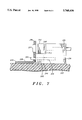
- FIG. 7 illustrates a greatly enlarged simplified sectional side view of the optoelectronic mount of FIG. 6.
- FIGS. 1 and 2 illustrate a package 10 including an optoelectronic mount 12 affixed to an interconnect substrate 13.
- Optoelectronic mount 12 includes an optical fiber holder 14 affixed to interconnect substrate 13 and holding optical fibers 15, a photonic unit 17 and an insulative flexible substrate 18 coupling photonic unit 17 to interconnect substrate 13.
- Flexible substrate 18 has an end 19 to which photonic unit 17 is coupled and an opposing end 20. End 20 is bonded to interconnect substrate 13, while end 19 is coupled to optical fiber holder 14. In this manner, optical devices can be incorporated with standard electrical components.
- photonic unit 17 can be any suitable photonic device or array of photonic devices including photo-transmitters, photo-receivers, or a combination thereof.
- a photo-transmitter can be any suitable device, such as a vertical cavity surface emitting laser (VCSEL), light emitting diode (LED), or the like.
- VCSEL vertical cavity surface emitting laser
- LED light emitting diode
- any suitable photo-receiving device can be used, such as a photodiode, e.g., P-I-N diode, PN diode, or the like.
- photonic unit 17 can be a broad range of photoactive devices capable of transmitting and receiving.
- Photonic unit 17 is illustrated as an array spanning the plurality of optical fibers 15 carried by optical fiber carrier 14.
- the array can be of any suitable configuration.
- the array can be made of individual photonic devices that are assembled to form unit 17 or the array can be made an integral unit.
- Photonic unit 17 is mounted to insulative flexible substrate 18 so that working portions of the photonic devices of unit 17 are aligned to individual optical fibers 15.
- Optical fiber holder 14 holds optical fibers 15 in a periodic fashion corresponding to the photonic devices of photonic unit 17.
- Optical fibers 15 are held such that each input surface 22 (FIG. 3) of each fiber 15 is substantially flush with a front surface 23 of optical fiber holder 14.
- Alignment holes 24 are formed in front surface 23 on opposing sides of optical fibers 15. Alignment holes 24 are precisely positioned relative optical fibers 15, and receive alignment pins 25 to insure alignment of photonic unit 17 with optical fibers 15, as will be described presently.
- Optical fiber holder 14 can be molded as a single piece with the alignment holes and fiber holes formed by precisely aligned hot pins pushed through the piece. The fibers are then threaded through the holes, glued and polished at input surface 22. Another method of forming optical fiber holder 14 is to mold two halves, and glue the halves around fibers 15. The ends are then polished.
- Interconnect substrate 13 is any suitable substrate, such as a printed circuit board, a FR4 board, a ceramic interconnect board, or the like, carrying electronic components.
- interconnect substrate 13 may be a printed circuit board having a plurality of integrated circuit (IC) chips 27 to drive the photonic devices of photonic unit 17.
- IC chips 27 are coupled to photonic unit 17 by flexible substrate 18.
- flexible substrate 18 is preferably a tape automated bonding (TAB) tape include several elements or features, such as bonding pads, thermally conductive traces and electrical traces. Only metallic electrical traces 30 and flexible insulation 32 are shown, as each of the other elements are well known and are not needed for the description of the present invention other than to know they are present for electrical coupling to substrate 13 and IC chips 27 for example.
- TAB tape automated bonding
- Adhesion of electrical traces 30 to flexible insulation 32 is such that they will not delaminate or separate when insulative flexible substrate 18 is bent or positioned on optical fiber holder 14 or interconnect substrate 13.
- materials selected for fabrication of insulative flexible substrate 18 are generally temperature resistant.
- optoelectronic mount 10 will undergo an overmolding process. Temperatures and times of duration of the overmolding process typically range from 200-300 degrees Celsius with time ranges from 10-15 minutes. Thus, material selected for fabrication of insulative flexible substrate 18 need to be tolerant of these temperatures and times. However, it should be evident that materials that exceed these requirements or performance levels, are also usable.
- Photonic unit 17 is coupled directly to electrical traces 30 which provide signals from IC chips 27 controlling the operation thereof. Additionally, a window 35 is formed through electrical traces 30, thereby allowing light to pass between optical fibers 15 and photonic unit 17.
- Alignment openings 37 are formed in insulative flexible substrate 18 on opposing sides of window 35. Alignment holes 37 are precisely positioned relative to the photonic unit 17, which is precisely mounted on the flexible substrate.
- Accurate placement or alignment of insulative flexible substrate 18, and therefore photonic unit 17, to optical fiber holder 14 is achieved by the use of alignment pins 25.
- pins 25 extend concurrently through openings 37 formed proximate end 19 of flexible substrate 18, and openings 24 formed in optical fiber holder 14, thereby aligning insulative flexible substrate 18 and photonic unit 17 to optical fiber holder 14.
- Attachment of insulative flexible substrate 18 to optical fiber holder 14 is achieved by any suitable method or technique, such as an adhesive, e.g., epoxy, polyimide, or any ultraviolet curable adhesive, or the like.
- Insulative flexible substrate 18 is positioned by alignment pins 25 and affixed to optical fiber holder 14 by use of an adhesive. For example, an optically transparent epoxy is applied to surface 23 of optical fiber holder 14. Insulative flexible substrate 18 is subsequently applied to optical fiber holder 14 and aligned using pins 25.
- Package 110 is similar to package 10 described above, and includes an optoelectronic mount 112 affixed to an interconnect substrate 113.
- Optoelectronic mount 112 includes an optical fiber holder 114 affixed to interconnect substrate 113 and holding optical fibers 115, a photonic unit 117 and an insulative flexible substrate 118 coupling photonic unit 117 to interconnect substrate 113.
- Flexible substrate 118 has an end 119 proximate to which photonic unit 117 is coupled and an opposing end 120. End 120 is bonded to interconnect substrate 113, while end 119 is coupled to optical fiber holder 114.
- alignment holes 124 are formed in a front surface 123 of optical fiber holder 114, on opposing sides of optical fibers 115, and alignment holes 137 are formed through insulative flexible substrate 118 proximate end 119. Alignment holes 124 and 137 are precisely positioned relative optical fibers 115 and photonic unit 117 respectively, and receive alignment pins 125 to insure alignment of photonic unit 117 with optical fibers 115.
- Interconnect substrate 113 includes electronics elements, such as IC chips 127 to run the photonic devices of photonic unit 117. IC chips 127 are coupled to photonic unit 117 by flexible substrate 118.
- Package 110 differs from package 10 in that an optical element 140 is positioned intermediate optical fiber holder 114 and insulative flexible substrate 118 to shape the beam received from or transmitted to the optical fibers.
- large core fibers are used. This is prevalent when plastic optical fibers are used in place of glass optical fibers. Generally, plastic fibers have a larger core diameter.
- a light emitting device such as a light emitting diode or a laser
- an optical fiber is improved. This is particularly important in order to couple a beam from a vertical cavity surface emitting laser (VCSEL) into a multimode optical fiber, with the modes of the fiber all being excited at the input end.
- VCSEL vertical cavity surface emitting laser
- Focusing and divergence can be achieved by employing a diffractive optical element.
- Optical element 140 is preferably etched into a glass or plastic base 142 and positioned directly between photonic unit 17 and optical fiber 15.
- a plurality of optical elements 140 are etched in base 142 with each optical element 140 positioned to align directly between a photonic device and its associated optical fiber.
- alignment holes 144 are formed through base 142 on opposing sides of optical elements 140. Alignment openings 144 are precisely positioned relative to optical elements 140.
- alignment pins 125 are inserted concurrently through openings 137 formed proximate end 119 of flexible substrate 118, openings 144 formed in base 142, and openings 124 formed in optical fiber holder 114, thereby aligning insulative flexible substrate 118 and photonic unit 117 to optical fiber holder 114, with optical elements 140 formed in base 142 positioned therebetween.
- Package 210 is similar to package 110 described above, and includes an optoelectronic mount 212 affixed to an interconnect substrate 213.
- Optoelectronic mount 212 includes an optical fiber holder 214 affixed to interconnect substrate 213 and holding optical fibers 215, a photonic unit 217 and an insulative flexible substrate 218 coupling photonic unit 217 to interconnect substrate 213.
- Flexible substrate 218 has an end 219 proximate to which photonic unit 217 is coupled and an opposing end 220. End 220 is bonded to interconnect substrate 213, while end 219 is coupled to optical fiber holder 214.
- alignment holes 224 are formed in a front surface 223 of optical fiber holder 214, on opposing sides of optical fibers 215, and alignment holes 237 are formed through insulative flexible substrate 218 proximate end 219. Alignment holes 224 and 237 are precisely positioned relative optical fibers 215 and photonic unit 217 respectively, and receive alignment pins 225 to insure alignment of photonic unit 217 with optical fibers 215.
- Package 210 differs from package 110 in that an optical element 240 formed in a base 242 is positioned in a receptacle 244 formed in optical fiber holder 214 and extending from front surface 223.
- Receptacle 244 defines a precisely positioned slot 245 dimensioned to receive and position base 242 intermediate optical fibers 215 and insulative flexible substrate 218.
- Optical element 240 is generally identical to optical element 140 described previously, but is aligned by employing slot 245 of receptacle 244 instead of alignment openings. Alignment openings 224 extend through receptacle 244 on opposing sides of slot 245.
- insulative flexible substrate 218 and therefore photonic unit 217, base 242 and therefore optical element 240, and optical fiber holder 214 is achieved by the use of alignment pins 225 and slot 245.
- base 142 is positioned intermediate optical fiber holder 114 and insulative flexible substrate 118 within slot 245.
- Slot 245 positions base 242 with optical elements 240 in alignment with optical fibers 215.
- Alignment pins 225 are inserted concurrently through openings 237 formed proximate end 219 of flexible substrate 218, and openings 224 formed in optical fiber holder 214, thereby aligning insulative flexible substrate 218 and photonic unit 217 to optical fiber holder 214, with optical elements 240 formed in base 242 positioned therebetween.
- the optoelectronic mount enables the incorporation of standard electronic components and optical components such that advantages of the optical components can be utilized. While the present disclosure illustrates a single optoelectronic mount, it will be understood by those skilled in the art that the unit may be used in either or both of an optical transmitter and an optical receiver. Further it should be noted that the method and apparatus of the present invention allow this integration in a cost effective manner by providing a way of eliminating costly steps carried out by hand and to automate the remaining manufacturing steps thus making the entire process highly manufacturable.
Abstract
Description
Claims (18)
Priority Applications (1)
| Application Number | Priority Date | Filing Date | Title |
|---|---|---|---|
| US08/753,311 US5768456A (en) | 1996-11-22 | 1996-11-22 | Optoelectronic package including photonic device mounted in flexible substrate |
Applications Claiming Priority (1)
| Application Number | Priority Date | Filing Date | Title |
|---|---|---|---|
| US08/753,311 US5768456A (en) | 1996-11-22 | 1996-11-22 | Optoelectronic package including photonic device mounted in flexible substrate |
Publications (1)
| Publication Number | Publication Date |
|---|---|
| US5768456A true US5768456A (en) | 1998-06-16 |
Family
ID=25030102
Family Applications (1)
| Application Number | Title | Priority Date | Filing Date |
|---|---|---|---|
| US08/753,311 Expired - Fee Related US5768456A (en) | 1996-11-22 | 1996-11-22 | Optoelectronic package including photonic device mounted in flexible substrate |
Country Status (1)
| Country | Link |
|---|---|
| US (1) | US5768456A (en) |
Cited By (81)
| Publication number | Priority date | Publication date | Assignee | Title |
|---|---|---|---|---|
| US5933558A (en) * | 1997-05-22 | 1999-08-03 | Motorola, Inc. | Optoelectronic device and method of assembly |
| US5940562A (en) * | 1996-03-12 | 1999-08-17 | Minnesota Mining And Manufacturing Company | Stubless optoelectronic device receptacle |
| US5940046A (en) * | 1997-04-14 | 1999-08-17 | The United States Of America As Represented By The Secretary Of The Navy | Standardized modular antenna system |
| EP0982610A2 (en) * | 1998-08-24 | 2000-03-01 | Hewlett-Packard Company | Optical subassembly for use in fiber optic data transmission and reception |
| EP1028341A2 (en) * | 1999-02-11 | 2000-08-16 | Hewlett-Packard Company | Integrated packaging system for optical communications devices that provides automatic alignment with optical fibers |
| EP1063547A1 (en) * | 1999-06-25 | 2000-12-27 | Lucent Technologies Inc. | Plastic packaged optoelectronic device |
| WO2001033272A1 (en) * | 1999-11-01 | 2001-05-10 | Cielo Communications, Inc. | Optical device using chip-on-board technology |
| WO2002025335A1 (en) * | 2000-09-21 | 2002-03-28 | Corona Optical Systems, Inc. | Electro-optic interconnect circuit board |
| WO2002025341A1 (en) * | 2000-09-21 | 2002-03-28 | Corona Optical Systems, Inc. | Method to align optical components to a substrate and other optical components |
| WO2002029465A1 (en) * | 2000-10-05 | 2002-04-11 | Corona Optical Systems, Inc. | Transparent substrate and hinged optical assembly |
| US6406195B1 (en) * | 1999-10-14 | 2002-06-18 | Digital Optics Corporation | Interface between opto-electronic devices and fibers |
| US6411758B1 (en) * | 2000-01-31 | 2002-06-25 | Motorola, Inc. | Method and apparatus for aligning a waveguide to a device |
| WO2002052909A2 (en) * | 2000-12-26 | 2002-07-04 | Emcore Corporation | Flexible printed circuit board |
| US20020110323A1 (en) * | 2001-02-13 | 2002-08-15 | Koichiro Kishima | Optical coupling device |
| US6459842B1 (en) | 2000-12-13 | 2002-10-01 | Teraconnect, Inc. | Packaging system for two-dimensional optoelectronic arrays |
| US20020159707A1 (en) * | 2000-02-28 | 2002-10-31 | Onix Microsystems, Inc. | Floating optical carrier |
| US6478625B2 (en) * | 2000-07-11 | 2002-11-12 | Bernard R. Tolmie | Electrical-optical hybrid connector |
| WO2002103427A2 (en) * | 2000-12-26 | 2002-12-27 | Emcore Corporation | Optoelectronic mounting structure |
| US6508595B1 (en) | 2000-05-11 | 2003-01-21 | International Business Machines Corporation | Assembly of opto-electronic module with improved heat sink |
| US20030026081A1 (en) * | 2001-08-03 | 2003-02-06 | National Semiconductor Corporation | Ceramic optical sub-assembly for optoelectronic modules |
| US6527456B1 (en) | 1999-10-13 | 2003-03-04 | Teraconnect, Inc. | Cluster integration approach to optical transceiver arrays and fiber bundles |
| US20030102157A1 (en) * | 2001-12-04 | 2003-06-05 | Rosenberg Paul K. | Circuit interconnect for optoelectronic device for controlled impedance at high frequencies |
| US20030129872A1 (en) * | 2002-01-07 | 2003-07-10 | Tolmie Bernard R. | Hybrid connector system and method |
| US20030142929A1 (en) * | 2002-01-22 | 2003-07-31 | Meir Bartur | Flex board interface to an optical module |
| US6601998B2 (en) | 2000-12-13 | 2003-08-05 | Teraconnect, Inc | Optical waveguide assembly for interfacing a two-dimensional optoelectronic array to fiber bundles |
| US20030147601A1 (en) * | 2002-02-01 | 2003-08-07 | Meir Bartur | Hybrid optical module employing integration of electronic circuitry with active optical devices |
| US6617518B2 (en) * | 2001-11-02 | 2003-09-09 | Jds Uniphase Corporaton | Enhanced flex cable |
| WO2003076998A1 (en) * | 2002-03-08 | 2003-09-18 | Infineon Technologies Ag | Optoelectronic module and plug arrangement |
| US20030180013A1 (en) * | 2002-03-19 | 2003-09-25 | Rosenberg Paul K. | Transistor outline package with exteriorly mounted risistors |
| US20030179558A1 (en) * | 2002-03-19 | 2003-09-25 | Giorgio Giaretta | Transmission line with integrated connection pads for circuit elements |
| US20030198427A1 (en) * | 2002-04-18 | 2003-10-23 | Bragg William David | Flexible optical circuit apparatus and method |
| US20030214860A1 (en) * | 2002-03-19 | 2003-11-20 | Finisar Corporation | Circuit board having traces with distinct transmission impedances |
| US20030227988A1 (en) * | 2002-01-25 | 2003-12-11 | Ravi Subrahmanyan | Jitter and wander reduction apparatus |
| US20040005124A1 (en) * | 2002-06-17 | 2004-01-08 | Kendra Gallup | Actively aligned optoelectronic device |
| US6676302B2 (en) * | 2001-09-17 | 2004-01-13 | Stratos Lightwave, Inc. | Method of constructing a fiber optics communications module |
| US20040057678A1 (en) * | 2002-08-30 | 2004-03-25 | Morris James E. | Optical and mechanical interface between opto-electronic devices and fibers |
| US6712527B1 (en) | 2000-01-12 | 2004-03-30 | International Business Machines Corporation | Fiber optic connections and method for using same |
| US20040067030A1 (en) * | 2002-10-02 | 2004-04-08 | Lakshman Rathnam | High-density fiber-optic module with multi-fold flexible circuit |
| US6729771B2 (en) | 2001-12-17 | 2004-05-04 | Stratos Lightwave, Inc. | Parallel optics subassembly having at least twelve lenses |
| US6739760B2 (en) | 2001-09-17 | 2004-05-25 | Stratos International, Inc. | Parallel fiber optics communications module |
| US20040136725A1 (en) * | 2002-12-12 | 2004-07-15 | Seiko Epson Corporation | Optical communication device |
| US6767142B2 (en) * | 2000-10-26 | 2004-07-27 | Fci | Optoelectronic emitter-receiver device |
| US20040146253A1 (en) * | 2003-01-28 | 2004-07-29 | Wang Charlie X. | Method and apparatus for parallel optical transceiver module assembly |
| JP2004354532A (en) * | 2003-05-27 | 2004-12-16 | Seiko Epson Corp | Optical module, its manufacturing method, optical communication device, and electronic apparatus |
| US20040264886A1 (en) * | 2003-06-26 | 2004-12-30 | Michael Powers | Low cost package design for fiber coupled optical component |
| US20050013560A1 (en) * | 2003-07-15 | 2005-01-20 | National Semiconductor Corporation | Opto-electronic module form factor having adjustable optical plane height |
| US20050018972A1 (en) * | 2000-12-26 | 2005-01-27 | Anderson Gene R. | Housing and mounting structure |
| US20050025435A1 (en) * | 2003-05-14 | 2005-02-03 | Seiko Epson Corporation | Optical module and manufacturing method of the same, optical-communication apparatus, and electronic apparatus |
| US20050025434A1 (en) * | 2003-07-31 | 2005-02-03 | International Business Machines Corporation | Method and apparatus for providing optoelectronic communication with an electronic device |
| US20050051598A1 (en) * | 2003-09-05 | 2005-03-10 | Trebor Heminway | Solder preform for low heat stress laser solder attachment |
| WO2005057262A1 (en) * | 2003-12-15 | 2005-06-23 | Nec Corporation | Optical module and production method therefor |
| US6910812B2 (en) | 2001-05-15 | 2005-06-28 | Peregrine Semiconductor Corporation | Small-scale optoelectronic package |
| US20050175297A1 (en) * | 2001-08-03 | 2005-08-11 | National Semiconductor Corporation | Optical sub-assembly for opto-electronic modules |
| US20050205957A1 (en) * | 2003-01-31 | 2005-09-22 | Morris Terrel L | Integrated VCSELs on traditional VLSI packaging |
| US20050254745A1 (en) * | 2004-05-14 | 2005-11-17 | Karl Schrodinger | Optoelectronic module and optoelectronic system |
| US20060028926A1 (en) * | 2004-08-04 | 2006-02-09 | Fujitsu Limited | Substrate, substrate adapted for interconnecting optical elements and optical module |
| US7021838B2 (en) | 2003-12-16 | 2006-04-04 | Matsushita Electric Industrial Co., Ltd. | Optimizing alignment of an optical fiber to an optical output port |
| US20060110110A1 (en) * | 2004-11-22 | 2006-05-25 | Yi Robert H | Optical turn system for optoelectronic modules |
| US7056032B2 (en) | 2001-09-17 | 2006-06-06 | Stratos International, Inc. | Transceiver assembly for use in fiber optics communications |
| US20060140534A1 (en) * | 2001-08-03 | 2006-06-29 | National Semiconductor Corporation | Ceramic optical sub-assembly for optoelectronic modules |
| US7073955B1 (en) | 2001-09-17 | 2006-07-11 | Stratos International, Inc. | Transceiver assembly for use in fiber optics communications |
| US7073954B1 (en) | 2001-09-17 | 2006-07-11 | Stratos International, Inc. | Transceiver assembly for use in fiber optics communications |
| US20060204177A1 (en) * | 2005-03-14 | 2006-09-14 | Matsushita Electric Industrial Co., Ltd. | Low cost, high precision multi-point optical component attachment |
| US20060237133A1 (en) * | 2001-07-19 | 2006-10-26 | Takayoshi Akamatsu | Methods for making laminated member for circuit board, making circuit board and laminating flexible film |
| US7128474B2 (en) * | 2001-11-13 | 2006-10-31 | Avago Technologies Fiber Ip (Singapore) Pte. Ltd. | Optical device, enclosure and method of fabricating |
| US20060251360A1 (en) * | 2005-05-06 | 2006-11-09 | Daoqiang Lu | Flip-chip mountable optical connector for chip-to-chip optical interconnectability |
| US20070031091A1 (en) * | 2005-08-04 | 2007-02-08 | Nec Electronics Corporation | Optical module with flexible substrate |
| US7254149B2 (en) | 2002-03-19 | 2007-08-07 | Finisar Corporation | Submount, pedestal, and bond wire assembly for a transistor outline package with reduced bond wire inductance |
| US7284913B2 (en) | 2003-07-14 | 2007-10-23 | Matsushita Electric Industrial Co., Ltd. | Integrated fiber attach pad for optical package |
| JP2007293018A (en) * | 2006-04-25 | 2007-11-08 | Nec Corp | Optoelectric composite module and optical i/o apparatus |
| JP2008170868A (en) * | 2007-01-15 | 2008-07-24 | Nec Corp | Optical waveguide type module |
| US20090297103A1 (en) * | 2008-06-02 | 2009-12-03 | Avago Technologies Fiber Ip (Singapore) Pte. Ltd. | Optical subassembly for an electro-optical assembly |
| US20110182546A1 (en) * | 2010-01-26 | 2011-07-28 | Hitachi Cable, Ltd. | Photoelectric conversion device |
| US8233757B2 (en) | 2001-10-23 | 2012-07-31 | Digitaloptics Corporation East | Wafer based optical chassis and associated methods |
| US20120251038A1 (en) * | 2011-03-29 | 2012-10-04 | Nitto Denko Corporation | Opto-electric hybrid board and manufacturing method therefor |
| US20120286904A1 (en) * | 2009-05-09 | 2012-11-15 | Fujitsu Limited | Connection terminal and transmission line |
| US20140126863A1 (en) * | 2012-11-07 | 2014-05-08 | Silicon Image, Inc. | Methods and apparatuses to provide an electro-optical alignment |
| US20140212086A1 (en) * | 2013-01-28 | 2014-07-31 | Hitachi Metals, Ltd. | Optical module |
| US20140270656A1 (en) * | 2013-03-18 | 2014-09-18 | Fujitsu Limited | Electronic device and optical connector |
| US10620377B1 (en) * | 2015-04-01 | 2020-04-14 | National Technology & Engineering Solutions Of Sandia, Llc | Kinematic chip to chip bonding |
| JP2021015176A (en) * | 2019-07-11 | 2021-02-12 | 日本電気株式会社 | Optical module and manufacturing method for optical module |
Citations (2)
| Publication number | Priority date | Publication date | Assignee | Title |
|---|---|---|---|---|
| US5249245A (en) * | 1992-08-31 | 1993-09-28 | Motorola, Inc. | Optoelectroinc mount including flexible substrate and method for making same |
| US5625734A (en) * | 1995-05-31 | 1997-04-29 | Motorola | Optoelectronic interconnect device and method of making |
-
1996
- 1996-11-22 US US08/753,311 patent/US5768456A/en not_active Expired - Fee Related
Patent Citations (2)
| Publication number | Priority date | Publication date | Assignee | Title |
|---|---|---|---|---|
| US5249245A (en) * | 1992-08-31 | 1993-09-28 | Motorola, Inc. | Optoelectroinc mount including flexible substrate and method for making same |
| US5625734A (en) * | 1995-05-31 | 1997-04-29 | Motorola | Optoelectronic interconnect device and method of making |
Cited By (171)
| Publication number | Priority date | Publication date | Assignee | Title |
|---|---|---|---|---|
| US5940562A (en) * | 1996-03-12 | 1999-08-17 | Minnesota Mining And Manufacturing Company | Stubless optoelectronic device receptacle |
| US5940046A (en) * | 1997-04-14 | 1999-08-17 | The United States Of America As Represented By The Secretary Of The Navy | Standardized modular antenna system |
| US5933558A (en) * | 1997-05-22 | 1999-08-03 | Motorola, Inc. | Optoelectronic device and method of assembly |
| EP0982610A3 (en) * | 1998-08-24 | 2003-01-02 | Agilent Technologies, Inc. (a Delaware corporation) | Optical subassembly for use in fiber optic data transmission and reception |
| EP0982610A2 (en) * | 1998-08-24 | 2000-03-01 | Hewlett-Packard Company | Optical subassembly for use in fiber optic data transmission and reception |
| EP1028341A3 (en) * | 1999-02-11 | 2004-07-21 | Agilent Technologies, Inc. (a Delaware corporation) | Integrated packaging system for optical communications devices that provides automatic alignment with optical fibers |
| JP4634562B2 (en) * | 1999-02-11 | 2011-02-16 | アバゴ・テクノロジーズ・ファイバー・アイピー(シンガポール)プライベート・リミテッド | Integrated packaging system for optical communication devices that automatically align with optical fibers |
| JP2000249883A (en) * | 1999-02-11 | 2000-09-14 | Agilent Technol Inc | Integrated packaging system for optical communication device to be automatically aligned to optical fiber |
| US6318909B1 (en) * | 1999-02-11 | 2001-11-20 | Agilent Technologies, Inc. | Integrated packaging system for optical communications devices that provides automatic alignment with optical fibers |
| US20020021874A1 (en) * | 1999-02-11 | 2002-02-21 | Giboney Kirk S. | Integrated packaging system for optical communications devices that provides automatic alignment with optical fibers |
| US7380994B2 (en) * | 1999-02-11 | 2008-06-03 | Avago Technologies Fiber Ip Pte Ltd | Integrated packaging system for optical communications devices that provides automatic alignment with optical fibers |
| EP1028341A2 (en) * | 1999-02-11 | 2000-08-16 | Hewlett-Packard Company | Integrated packaging system for optical communications devices that provides automatic alignment with optical fibers |
| US20060008214A1 (en) * | 1999-02-11 | 2006-01-12 | Giboney Kirk S | Integrated packaging system for optical communications devices that provides automatic alignment with optical fibers |
| US6835003B2 (en) | 1999-02-11 | 2004-12-28 | Agilent Technologies, Inc. | Integrated packaging system for optical communications devices that provides automatic alignment with optical fibers |
| EP1063547A1 (en) * | 1999-06-25 | 2000-12-27 | Lucent Technologies Inc. | Plastic packaged optoelectronic device |
| US6517258B1 (en) | 1999-06-25 | 2003-02-11 | Agere Systems Inc. | Plastic packaged optoelectronic device |
| US6527456B1 (en) | 1999-10-13 | 2003-03-04 | Teraconnect, Inc. | Cluster integration approach to optical transceiver arrays and fiber bundles |
| US6406195B1 (en) * | 1999-10-14 | 2002-06-18 | Digital Optics Corporation | Interface between opto-electronic devices and fibers |
| US6588945B2 (en) | 1999-10-14 | 2003-07-08 | Digital Optics Corporation | Interface between opto-electronic devices and fibers |
| US20040240803A1 (en) * | 1999-11-01 | 2004-12-02 | Rechberger David L. | Use of chip-on-board technology to mount optical transmitting and detecting devices with a protective covering with multiple optical interface options |
| WO2001033272A1 (en) * | 1999-11-01 | 2001-05-10 | Cielo Communications, Inc. | Optical device using chip-on-board technology |
| US6712527B1 (en) | 2000-01-12 | 2004-03-30 | International Business Machines Corporation | Fiber optic connections and method for using same |
| US6411758B1 (en) * | 2000-01-31 | 2002-06-25 | Motorola, Inc. | Method and apparatus for aligning a waveguide to a device |
| US20020159707A1 (en) * | 2000-02-28 | 2002-10-31 | Onix Microsystems, Inc. | Floating optical carrier |
| US6853779B2 (en) | 2000-02-28 | 2005-02-08 | Onix Microsystems | Floating optical carrier |
| US6508595B1 (en) | 2000-05-11 | 2003-01-21 | International Business Machines Corporation | Assembly of opto-electronic module with improved heat sink |
| US6822875B2 (en) | 2000-05-11 | 2004-11-23 | International Business Machines Corporation | Assembly of opto-electronic module with improved heat sink |
| US6478625B2 (en) * | 2000-07-11 | 2002-11-12 | Bernard R. Tolmie | Electrical-optical hybrid connector |
| US6793409B2 (en) | 2000-09-21 | 2004-09-21 | Corona Optical Systems, Inc. | Method to align optical components to a substrate and other optical components |
| WO2002025335A1 (en) * | 2000-09-21 | 2002-03-28 | Corona Optical Systems, Inc. | Electro-optic interconnect circuit board |
| WO2002025341A1 (en) * | 2000-09-21 | 2002-03-28 | Corona Optical Systems, Inc. | Method to align optical components to a substrate and other optical components |
| US6547454B2 (en) | 2000-09-21 | 2003-04-15 | Corona Optical Systems, Inc. | Method to align optical components to a substrate and other optical components |
| US6600853B2 (en) * | 2000-09-21 | 2003-07-29 | Corona Optical Systems, Inc. | Electro-optic interconnect circuit board |
| WO2002029465A1 (en) * | 2000-10-05 | 2002-04-11 | Corona Optical Systems, Inc. | Transparent substrate and hinged optical assembly |
| US6450704B1 (en) | 2000-10-05 | 2002-09-17 | Corona Optical Systems, Inc. | Transparent substrate and hinged optical assembly |
| US6843608B2 (en) | 2000-10-05 | 2005-01-18 | Corona Optical Systems, Inc. | Transparent substrate and hinged optical assembly |
| US20040208461A1 (en) * | 2000-10-05 | 2004-10-21 | Corona Optical Systems, Inc. | Transparent substrate and hinged optical assembly |
| US6729776B2 (en) * | 2000-10-05 | 2004-05-04 | Corona Optical Systems, Inc. | Transparent substrate and hinged optical assembly |
| US6767142B2 (en) * | 2000-10-26 | 2004-07-27 | Fci | Optoelectronic emitter-receiver device |
| US6601998B2 (en) | 2000-12-13 | 2003-08-05 | Teraconnect, Inc | Optical waveguide assembly for interfacing a two-dimensional optoelectronic array to fiber bundles |
| US6459842B1 (en) | 2000-12-13 | 2002-10-01 | Teraconnect, Inc. | Packaging system for two-dimensional optoelectronic arrays |
| US20030075355A1 (en) * | 2000-12-26 | 2003-04-24 | Anderson Gene R. | An apparatus and method of using flexible printed circuit board in optical transceiver device |
| WO2002052909A3 (en) * | 2000-12-26 | 2003-10-09 | Emcore Corp | Flexible printed circuit board |
| WO2002103427A3 (en) * | 2000-12-26 | 2003-10-30 | Emcore Corp | Optoelectronic mounting structure |
| WO2002052909A2 (en) * | 2000-12-26 | 2002-07-04 | Emcore Corporation | Flexible printed circuit board |
| US6799902B2 (en) | 2000-12-26 | 2004-10-05 | Emcore Corporation | Optoelectronic mounting structure |
| US20050018972A1 (en) * | 2000-12-26 | 2005-01-27 | Anderson Gene R. | Housing and mounting structure |
| WO2002103427A2 (en) * | 2000-12-26 | 2002-12-27 | Emcore Corporation | Optoelectronic mounting structure |
| US7027687B2 (en) * | 2001-02-13 | 2006-04-11 | Sony Corporation | Optical coupling device |
| US20020110323A1 (en) * | 2001-02-13 | 2002-08-15 | Koichiro Kishima | Optical coupling device |
| US6910812B2 (en) | 2001-05-15 | 2005-06-28 | Peregrine Semiconductor Corporation | Small-scale optoelectronic package |
| US7534361B2 (en) * | 2001-07-19 | 2009-05-19 | Toray Industries, Inc. | Methods for making laminated member for circuit board, making circuit board and laminating flexible film |
| US20060237133A1 (en) * | 2001-07-19 | 2006-10-26 | Takayoshi Akamatsu | Methods for making laminated member for circuit board, making circuit board and laminating flexible film |
| US7023705B2 (en) | 2001-08-03 | 2006-04-04 | National Semiconductor Corporation | Ceramic optical sub-assembly for optoelectronic modules |
| US20060140534A1 (en) * | 2001-08-03 | 2006-06-29 | National Semiconductor Corporation | Ceramic optical sub-assembly for optoelectronic modules |
| US7086788B2 (en) * | 2001-08-03 | 2006-08-08 | National Semiconductor Corporation | Optical sub-assembly for opto-electronic modules |
| US20030026081A1 (en) * | 2001-08-03 | 2003-02-06 | National Semiconductor Corporation | Ceramic optical sub-assembly for optoelectronic modules |
| US20050175297A1 (en) * | 2001-08-03 | 2005-08-11 | National Semiconductor Corporation | Optical sub-assembly for opto-electronic modules |
| US7269027B2 (en) | 2001-08-03 | 2007-09-11 | National Semiconductor Corporation | Ceramic optical sub-assembly for optoelectronic modules |
| US20040120659A1 (en) * | 2001-09-17 | 2004-06-24 | Stratos Lightwave, Inc. | Parallel fiber optics communications module |
| US20060153505A1 (en) * | 2001-09-17 | 2006-07-13 | Stratos International, Inc. | Transceiver assembly for use in fiber optics communications |
| US7097365B2 (en) | 2001-09-17 | 2006-08-29 | Stratos International, Inc. | Transceiver assembly for use in fiber optics communications |
| US7056032B2 (en) | 2001-09-17 | 2006-06-06 | Stratos International, Inc. | Transceiver assembly for use in fiber optics communications |
| US20060159403A1 (en) * | 2001-09-17 | 2006-07-20 | Stratos International, Inc. | Transceiver assembly for use in fiber optics communications |
| US20040105629A1 (en) * | 2001-09-17 | 2004-06-03 | Stratos Lightwave, Inc. | Parallel fiber optics communications module |
| US20040105631A1 (en) * | 2001-09-17 | 2004-06-03 | Stratos Lightware, Inc. | Parallel fiber optics communications module |
| US20040105630A1 (en) * | 2001-09-17 | 2004-06-03 | Stratos Lightwave, Inc. | Parallel fiber optics communications module |
| US6808318B2 (en) | 2001-09-17 | 2004-10-26 | Stratos International, Inc. | Parallel fiber optics communications module |
| US6808320B2 (en) | 2001-09-17 | 2004-10-26 | Stratos International, Inc. | Parallel fiber optics communications module |
| US6808319B2 (en) | 2001-09-17 | 2004-10-26 | Stratos International, Inc. | Parallel fiber optics communications module |
| US6808317B2 (en) | 2001-09-17 | 2004-10-26 | Stratos International, Inc. | Parallel fiber optics communications module |
| US7101090B2 (en) | 2001-09-17 | 2006-09-05 | Stratos International, Inc. | Transceiver assembly for use in fiber optics communications |
| US6739760B2 (en) | 2001-09-17 | 2004-05-25 | Stratos International, Inc. | Parallel fiber optics communications module |
| US20060153506A1 (en) * | 2001-09-17 | 2006-07-13 | Stratos International, Inc. | Transceiver assembly for use in fiber optics communications |
| US20060147159A1 (en) * | 2001-09-17 | 2006-07-06 | Stratos International, Inc | Transceiver assembly for use in fiber optics communications |
| US6676302B2 (en) * | 2001-09-17 | 2004-01-13 | Stratos Lightwave, Inc. | Method of constructing a fiber optics communications module |
| US7073955B1 (en) | 2001-09-17 | 2006-07-11 | Stratos International, Inc. | Transceiver assembly for use in fiber optics communications |
| US7073954B1 (en) | 2001-09-17 | 2006-07-11 | Stratos International, Inc. | Transceiver assembly for use in fiber optics communications |
| US8233757B2 (en) | 2001-10-23 | 2012-07-31 | Digitaloptics Corporation East | Wafer based optical chassis and associated methods |
| US6617518B2 (en) * | 2001-11-02 | 2003-09-09 | Jds Uniphase Corporaton | Enhanced flex cable |
| US7128474B2 (en) * | 2001-11-13 | 2006-10-31 | Avago Technologies Fiber Ip (Singapore) Pte. Ltd. | Optical device, enclosure and method of fabricating |
| US20050116239A1 (en) * | 2001-12-04 | 2005-06-02 | Rosenberg Paul K. | Circuit interconnect for optoelectronic device |
| US20030102157A1 (en) * | 2001-12-04 | 2003-06-05 | Rosenberg Paul K. | Circuit interconnect for optoelectronic device for controlled impedance at high frequencies |
| US7211830B2 (en) * | 2001-12-04 | 2007-05-01 | Finisar Corporation | Circuit interconnect for optoelectronic device |
| US6876004B2 (en) * | 2001-12-04 | 2005-04-05 | Finisar Corporation | Circuit interconnect for optoelectronic device for controlled impedance at high frequencies |
| US6729771B2 (en) | 2001-12-17 | 2004-05-04 | Stratos Lightwave, Inc. | Parallel optics subassembly having at least twelve lenses |
| US6821146B2 (en) | 2002-01-07 | 2004-11-23 | Bernard R. Tolmie | Hybrid connector system and method |
| US20030129872A1 (en) * | 2002-01-07 | 2003-07-10 | Tolmie Bernard R. | Hybrid connector system and method |
| US20030142929A1 (en) * | 2002-01-22 | 2003-07-31 | Meir Bartur | Flex board interface to an optical module |
| WO2003062866A2 (en) * | 2002-01-22 | 2003-07-31 | Zonu, Inc. | Flex board interface to an optical module |
| WO2003062866A3 (en) * | 2002-01-22 | 2003-10-30 | Zonu Inc | Flex board interface to an optical module |
| US20030227988A1 (en) * | 2002-01-25 | 2003-12-11 | Ravi Subrahmanyan | Jitter and wander reduction apparatus |
| US7212599B2 (en) | 2002-01-25 | 2007-05-01 | Applied Micro Circuits Corporation | Jitter and wander reduction apparatus |
| US20030147601A1 (en) * | 2002-02-01 | 2003-08-07 | Meir Bartur | Hybrid optical module employing integration of electronic circuitry with active optical devices |
| WO2003076998A1 (en) * | 2002-03-08 | 2003-09-18 | Infineon Technologies Ag | Optoelectronic module and plug arrangement |
| US7371012B2 (en) | 2002-03-08 | 2008-05-13 | Infineon Technologies Ag | Optoelectronic module and plug arrangement |
| US20060013542A1 (en) * | 2002-03-08 | 2006-01-19 | Infineon Technologies Ag | Optoelectronic module and plug arrangement |
| US20030179558A1 (en) * | 2002-03-19 | 2003-09-25 | Giorgio Giaretta | Transmission line with integrated connection pads for circuit elements |
| US6932518B2 (en) * | 2002-03-19 | 2005-08-23 | Finisar Corporation | Circuit board having traces with distinct transmission impedances |
| US20030214860A1 (en) * | 2002-03-19 | 2003-11-20 | Finisar Corporation | Circuit board having traces with distinct transmission impedances |
| US7042067B2 (en) | 2002-03-19 | 2006-05-09 | Finisar Corporation | Transmission line with integrated connection pads for circuit elements |
| US20030180013A1 (en) * | 2002-03-19 | 2003-09-25 | Rosenberg Paul K. | Transistor outline package with exteriorly mounted risistors |
| US7254149B2 (en) | 2002-03-19 | 2007-08-07 | Finisar Corporation | Submount, pedestal, and bond wire assembly for a transistor outline package with reduced bond wire inductance |
| US7044657B2 (en) | 2002-03-19 | 2006-05-16 | Finisar Corporation | Transistor outline package with exteriorly mounted resistors |
| US7532782B2 (en) * | 2002-04-18 | 2009-05-12 | Pivotal Decisions Llc | Flexible optical circuit apparatus and method |
| US20030198427A1 (en) * | 2002-04-18 | 2003-10-23 | Bragg William David | Flexible optical circuit apparatus and method |
| US20040005124A1 (en) * | 2002-06-17 | 2004-01-08 | Kendra Gallup | Actively aligned optoelectronic device |
| US6955480B2 (en) | 2002-06-17 | 2005-10-18 | Agilent Technologies, Inc. | Actively aligned optoelectronic device |
| US20040057678A1 (en) * | 2002-08-30 | 2004-03-25 | Morris James E. | Optical and mechanical interface between opto-electronic devices and fibers |
| US6821028B2 (en) | 2002-08-30 | 2004-11-23 | Digital Optics Corp. | Optical and mechanical interface between opto-electronic devices and fibers |
| US7070341B2 (en) | 2002-10-02 | 2006-07-04 | Emcore Corporation | High-density fiber-optic module with multi-fold flexible circuit |
| US20040067030A1 (en) * | 2002-10-02 | 2004-04-08 | Lakshman Rathnam | High-density fiber-optic module with multi-fold flexible circuit |
| US7127142B2 (en) | 2002-12-12 | 2006-10-24 | Seiko Epson Corporation | Optical communication device |
| US20040136725A1 (en) * | 2002-12-12 | 2004-07-15 | Seiko Epson Corporation | Optical communication device |
| WO2004070428A3 (en) * | 2003-01-28 | 2004-12-02 | Emcore Corp | Method and apparatus for parallel optical transceiver module assembly |
| WO2004070428A2 (en) * | 2003-01-28 | 2004-08-19 | Emcore Corporation | Method and apparatus for parallel optical transceiver module assembly |
| US20040146253A1 (en) * | 2003-01-28 | 2004-07-29 | Wang Charlie X. | Method and apparatus for parallel optical transceiver module assembly |
| US20050205957A1 (en) * | 2003-01-31 | 2005-09-22 | Morris Terrel L | Integrated VCSELs on traditional VLSI packaging |
| US20050025435A1 (en) * | 2003-05-14 | 2005-02-03 | Seiko Epson Corporation | Optical module and manufacturing method of the same, optical-communication apparatus, and electronic apparatus |
| US7103249B2 (en) | 2003-05-14 | 2006-09-05 | Seiko Epson Corporation | Optical module and manufacturing method of the same, optical-communication apparatus, and electronic apparatus |
| JP2004354532A (en) * | 2003-05-27 | 2004-12-16 | Seiko Epson Corp | Optical module, its manufacturing method, optical communication device, and electronic apparatus |
| US20050002618A1 (en) * | 2003-05-27 | 2005-01-06 | Seiko Epson Corporation | Optical module, method of manufacturing the same, optical communication device and electronic device using the same |
| US7160035B2 (en) | 2003-05-27 | 2007-01-09 | Seiko Epson Corporation | Optical module, method of manufacturing the same, optical communication device and electronic device using the same |
| US6883978B2 (en) * | 2003-06-26 | 2005-04-26 | Matsushita Electric Industrial Co., Ltd. | Low cost package design for fiber coupled optical component |
| US20040264886A1 (en) * | 2003-06-26 | 2004-12-30 | Michael Powers | Low cost package design for fiber coupled optical component |
| US7284913B2 (en) | 2003-07-14 | 2007-10-23 | Matsushita Electric Industrial Co., Ltd. | Integrated fiber attach pad for optical package |
| US7156562B2 (en) | 2003-07-15 | 2007-01-02 | National Semiconductor Corporation | Opto-electronic module form factor having adjustable optical plane height |
| US20050013560A1 (en) * | 2003-07-15 | 2005-01-20 | National Semiconductor Corporation | Opto-electronic module form factor having adjustable optical plane height |
| US7128472B2 (en) | 2003-07-31 | 2006-10-31 | International Business Machines Corporation | Method and apparatus for providing optoelectronic communication with an electronic device |
| US20050025434A1 (en) * | 2003-07-31 | 2005-02-03 | International Business Machines Corporation | Method and apparatus for providing optoelectronic communication with an electronic device |
| US7410088B2 (en) | 2003-09-05 | 2008-08-12 | Matsushita Electric Industrial, Co., Ltd. | Solder preform for low heat stress laser solder attachment |
| US20050051598A1 (en) * | 2003-09-05 | 2005-03-10 | Trebor Heminway | Solder preform for low heat stress laser solder attachment |
| WO2005057262A1 (en) * | 2003-12-15 | 2005-06-23 | Nec Corporation | Optical module and production method therefor |
| JPWO2005057262A1 (en) * | 2003-12-15 | 2007-08-23 | 日本電気株式会社 | Optical module and manufacturing method thereof |
| US7021838B2 (en) | 2003-12-16 | 2006-04-04 | Matsushita Electric Industrial Co., Ltd. | Optimizing alignment of an optical fiber to an optical output port |
| US20050254745A1 (en) * | 2004-05-14 | 2005-11-17 | Karl Schrodinger | Optoelectronic module and optoelectronic system |
| US7036999B2 (en) * | 2004-05-14 | 2006-05-02 | Schroedinger Karl | Optoelectronic module and optoelectronic system |
| US20060028926A1 (en) * | 2004-08-04 | 2006-02-09 | Fujitsu Limited | Substrate, substrate adapted for interconnecting optical elements and optical module |
| US7519243B2 (en) * | 2004-08-04 | 2009-04-14 | Fujitsu Limited | Substrate, substrate adapted for interconnecting optical elements and optical module |
| CN1779970B (en) * | 2004-11-22 | 2010-05-05 | 安华高科技杰纳勒尔Ip(新加坡)私人有限公司 | Optical rotation system for optoelectronic module |
| GB2421849B (en) * | 2004-11-22 | 2010-04-14 | Agilent Technologies Inc | Optoelectronic module and method of making such a module |
| GB2421849A (en) * | 2004-11-22 | 2006-07-05 | Agilent Technologies Inc | Optoelectronic Module and Method of Making Such a Module |
| US20060110110A1 (en) * | 2004-11-22 | 2006-05-25 | Yi Robert H | Optical turn system for optoelectronic modules |
| US20060204177A1 (en) * | 2005-03-14 | 2006-09-14 | Matsushita Electric Industrial Co., Ltd. | Low cost, high precision multi-point optical component attachment |
| US7263260B2 (en) | 2005-03-14 | 2007-08-28 | Matsushita Electric Industrial Co., Ltd. | Low cost, high precision multi-point optical component attachment |
| US20060251360A1 (en) * | 2005-05-06 | 2006-11-09 | Daoqiang Lu | Flip-chip mountable optical connector for chip-to-chip optical interconnectability |
| US7703991B2 (en) * | 2005-05-06 | 2010-04-27 | Intel Corporation | Flip-chip mountable optical connector for chip-to-chip optical interconnectability |
| US7260285B2 (en) * | 2005-08-04 | 2007-08-21 | Nec Electronics Corporation | Optical module with flexible substrate |
| US20070031091A1 (en) * | 2005-08-04 | 2007-02-08 | Nec Electronics Corporation | Optical module with flexible substrate |
| US7620272B2 (en) * | 2006-04-25 | 2009-11-17 | Nec Corporation | Photoelectric composite module and optical input/output device |
| JP2007293018A (en) * | 2006-04-25 | 2007-11-08 | Nec Corp | Optoelectric composite module and optical i/o apparatus |
| US20070280594A1 (en) * | 2006-04-25 | 2007-12-06 | Nec Corporation | Photoelectric composite module and optical input/output device |
| JP2008170868A (en) * | 2007-01-15 | 2008-07-24 | Nec Corp | Optical waveguide type module |
| US20090297103A1 (en) * | 2008-06-02 | 2009-12-03 | Avago Technologies Fiber Ip (Singapore) Pte. Ltd. | Optical subassembly for an electro-optical assembly |
| US7654753B2 (en) * | 2008-06-02 | 2010-02-02 | Avago Technologies Fiber Ip (Singapore) Pte. Ltd. | Optical subassembly for an electro-optical assembly |
| US20120286904A1 (en) * | 2009-05-09 | 2012-11-15 | Fujitsu Limited | Connection terminal and transmission line |
| US8491316B2 (en) * | 2009-05-09 | 2013-07-23 | Fujitsu Limited | Connection terminal and transmission line |
| US20110182546A1 (en) * | 2010-01-26 | 2011-07-28 | Hitachi Cable, Ltd. | Photoelectric conversion device |
| US9116314B2 (en) * | 2010-01-26 | 2015-08-25 | Hitachi Metals, Ltd. | Photoelectric conversion device |
| US8837873B2 (en) * | 2011-03-29 | 2014-09-16 | Nitto Denko Corporation | Opto-electric hybrid board and manufacturing method therefor |
| US20120251038A1 (en) * | 2011-03-29 | 2012-10-04 | Nitto Denko Corporation | Opto-electric hybrid board and manufacturing method therefor |
| US9497860B2 (en) * | 2012-11-07 | 2016-11-15 | Lattice Semiconductor Corporation | Methods and Apparatuses to provide an electro-optical alignment |
| US20140126863A1 (en) * | 2012-11-07 | 2014-05-08 | Silicon Image, Inc. | Methods and apparatuses to provide an electro-optical alignment |
| CN103969766A (en) * | 2013-01-28 | 2014-08-06 | 日立金属株式会社 | Optical module |
| US9104000B2 (en) * | 2013-01-28 | 2015-08-11 | Hitachi Metals, Ltd. | Optical module |
| US20140212086A1 (en) * | 2013-01-28 | 2014-07-31 | Hitachi Metals, Ltd. | Optical module |
| CN103969766B (en) * | 2013-01-28 | 2016-08-17 | 日立金属株式会社 | Optical module |
| US20140270656A1 (en) * | 2013-03-18 | 2014-09-18 | Fujitsu Limited | Electronic device and optical connector |
| US9360639B2 (en) * | 2013-03-18 | 2016-06-07 | Fujitsu Limited | Electronic device and optical connector |
| US10620377B1 (en) * | 2015-04-01 | 2020-04-14 | National Technology & Engineering Solutions Of Sandia, Llc | Kinematic chip to chip bonding |
| JP2021015176A (en) * | 2019-07-11 | 2021-02-12 | 日本電気株式会社 | Optical module and manufacturing method for optical module |
Similar Documents
| Publication | Publication Date | Title |
|---|---|---|
| US5768456A (en) | Optoelectronic package including photonic device mounted in flexible substrate | |
| US5625734A (en) | Optoelectronic interconnect device and method of making | |
| US5249245A (en) | Optoelectroinc mount including flexible substrate and method for making same | |
| US7118293B2 (en) | Optical module and manufacturing method of the same, optical communication device, opto-electrical hybrid integrated circuit, circuit board, and electronic apparatus | |
| US5337391A (en) | Optoelectronic sub-module and method of making same | |
| US5309537A (en) | Optoelectronic coupling device and method of making | |
| US5521992A (en) | Molded optical interconnect | |
| JP5270917B2 (en) | Optical assembly having optoelectronic device alignment function | |
| US5446814A (en) | Molded reflective optical waveguide | |
| JP3850569B2 (en) | Ferrule assembly and optical module | |
| EP0331331B1 (en) | Subassembly for optoelectronic devices | |
| EP2413171A1 (en) | Laterally coupled optical fiber component and processing method thereof | |
| JP2000082830A (en) | Optical subassembly for optical communication device and manufacture thereof | |
| JP2001515608A (en) | Receptacle for direct coupling of photoelectric element | |
| JPH08179171A (en) | Integrated mount, integrated mount assembly, photoelectronic package, and manufacture of integrated mount | |
| US5539200A (en) | Integrated optoelectronic substrate | |
| US6685363B2 (en) | Passive self-alignment technique for array laser transmitters and receivers for fiber optic applications | |
| JP2001356249A (en) | Device constituted of photodiode and optical fiber | |
| Ambrosy et al. | Silicon motherboards for multichannel optical modules | |
| JPH085872A (en) | Optical module and its production | |
| US6491446B1 (en) | Passive self-alignment technique for array laser transmitters and receivers for fiber optic applications | |
| US7519243B2 (en) | Substrate, substrate adapted for interconnecting optical elements and optical module | |
| US5500914A (en) | Optical interconnect unit and method or making | |
| JP2001343560A (en) | Optical module | |
| WO1998014813A1 (en) | Fiber optic array transmitter/receiver based on flexible circuit technology |
Legal Events
| Date | Code | Title | Description |
|---|---|---|---|
| AS | Assignment |
Owner name: MOTOROLA, INC., ILLINOIS Free format text: ASSIGNMENT OF ASSIGNORS INTEREST;ASSIGNORS:KNAPP, JAMES H.;FOLEY, BARBARA M.;REEL/FRAME:008288/0634 Effective date: 19961111 |
|
| CC | Certificate of correction | ||
| FPAY | Fee payment |
Year of fee payment: 4 |
|
| FPAY | Fee payment |
Year of fee payment: 8 |
|
| REMI | Maintenance fee reminder mailed | ||
| LAPS | Lapse for failure to pay maintenance fees | ||
| LAPS | Lapse for failure to pay maintenance fees |
Free format text: PATENT EXPIRED FOR FAILURE TO PAY MAINTENANCE FEES (ORIGINAL EVENT CODE: EXP.); ENTITY STATUS OF PATENT OWNER: LARGE ENTITY |
|
| STCH | Information on status: patent discontinuation |
Free format text: PATENT EXPIRED DUE TO NONPAYMENT OF MAINTENANCE FEES UNDER 37 CFR 1.362 |
|
| FP | Lapsed due to failure to pay maintenance fee |
Effective date: 20100616 |