US5776797A - Three-dimensional flexible assembly of integrated circuits - Google Patents
Three-dimensional flexible assembly of integrated circuits Download PDFInfo
- Publication number
- US5776797A US5776797A US08/887,430 US88743097A US5776797A US 5776797 A US5776797 A US 5776797A US 88743097 A US88743097 A US 88743097A US 5776797 A US5776797 A US 5776797A
- Authority
- US
- United States
- Prior art keywords
- chips
- flexible substrate
- substrate
- assembly
- integrated circuit
- Prior art date
- Legal status (The legal status is an assumption and is not a legal conclusion. Google has not performed a legal analysis and makes no representation as to the accuracy of the status listed.)
- Expired - Fee Related
Links
Images


Classifications
-
- H—ELECTRICITY
- H01—ELECTRIC ELEMENTS
- H01L—SEMICONDUCTOR DEVICES NOT COVERED BY CLASS H10
- H01L23/00—Details of semiconductor or other solid state devices
- H01L23/52—Arrangements for conducting electric current within the device in operation from one component to another, i.e. interconnections, e.g. wires, lead frames
- H01L23/538—Arrangements for conducting electric current within the device in operation from one component to another, i.e. interconnections, e.g. wires, lead frames the interconnection structure between a plurality of semiconductor chips being formed on, or in, insulating substrates
- H01L23/5387—Flexible insulating substrates
-
- H—ELECTRICITY
- H01—ELECTRIC ELEMENTS
- H01L—SEMICONDUCTOR DEVICES NOT COVERED BY CLASS H10
- H01L25/00—Assemblies consisting of a plurality of individual semiconductor or other solid state devices ; Multistep manufacturing processes thereof
- H01L25/03—Assemblies consisting of a plurality of individual semiconductor or other solid state devices ; Multistep manufacturing processes thereof all the devices being of a type provided for in the same subgroup of groups H01L27/00 - H01L33/00, or in a single subclass of H10K, H10N, e.g. assemblies of rectifier diodes
- H01L25/04—Assemblies consisting of a plurality of individual semiconductor or other solid state devices ; Multistep manufacturing processes thereof all the devices being of a type provided for in the same subgroup of groups H01L27/00 - H01L33/00, or in a single subclass of H10K, H10N, e.g. assemblies of rectifier diodes the devices not having separate containers
- H01L25/065—Assemblies consisting of a plurality of individual semiconductor or other solid state devices ; Multistep manufacturing processes thereof all the devices being of a type provided for in the same subgroup of groups H01L27/00 - H01L33/00, or in a single subclass of H10K, H10N, e.g. assemblies of rectifier diodes the devices not having separate containers the devices being of a type provided for in group H01L27/00
- H01L25/0657—Stacked arrangements of devices
-
- H—ELECTRICITY
- H01—ELECTRIC ELEMENTS
- H01L—SEMICONDUCTOR DEVICES NOT COVERED BY CLASS H10
- H01L2224/00—Indexing scheme for arrangements for connecting or disconnecting semiconductor or solid-state bodies and methods related thereto as covered by H01L24/00
- H01L2224/01—Means for bonding being attached to, or being formed on, the surface to be connected, e.g. chip-to-package, die-attach, "first-level" interconnects; Manufacturing methods related thereto
- H01L2224/10—Bump connectors; Manufacturing methods related thereto
- H01L2224/15—Structure, shape, material or disposition of the bump connectors after the connecting process
- H01L2224/16—Structure, shape, material or disposition of the bump connectors after the connecting process of an individual bump connector
- H01L2224/161—Disposition
- H01L2224/16151—Disposition the bump connector connecting between a semiconductor or solid-state body and an item not being a semiconductor or solid-state body, e.g. chip-to-substrate, chip-to-passive
- H01L2224/16221—Disposition the bump connector connecting between a semiconductor or solid-state body and an item not being a semiconductor or solid-state body, e.g. chip-to-substrate, chip-to-passive the body and the item being stacked
- H01L2224/16225—Disposition the bump connector connecting between a semiconductor or solid-state body and an item not being a semiconductor or solid-state body, e.g. chip-to-substrate, chip-to-passive the body and the item being stacked the item being non-metallic, e.g. insulating substrate with or without metallisation
-
- H—ELECTRICITY
- H01—ELECTRIC ELEMENTS
- H01L—SEMICONDUCTOR DEVICES NOT COVERED BY CLASS H10
- H01L2224/00—Indexing scheme for arrangements for connecting or disconnecting semiconductor or solid-state bodies and methods related thereto as covered by H01L24/00
- H01L2224/01—Means for bonding being attached to, or being formed on, the surface to be connected, e.g. chip-to-package, die-attach, "first-level" interconnects; Manufacturing methods related thereto
- H01L2224/26—Layer connectors, e.g. plate connectors, solder or adhesive layers; Manufacturing methods related thereto
- H01L2224/31—Structure, shape, material or disposition of the layer connectors after the connecting process
- H01L2224/32—Structure, shape, material or disposition of the layer connectors after the connecting process of an individual layer connector
- H01L2224/321—Disposition
- H01L2224/32135—Disposition the layer connector connecting between different semiconductor or solid-state bodies, i.e. chip-to-chip
- H01L2224/32145—Disposition the layer connector connecting between different semiconductor or solid-state bodies, i.e. chip-to-chip the bodies being stacked
-
- H—ELECTRICITY
- H01—ELECTRIC ELEMENTS
- H01L—SEMICONDUCTOR DEVICES NOT COVERED BY CLASS H10
- H01L2224/00—Indexing scheme for arrangements for connecting or disconnecting semiconductor or solid-state bodies and methods related thereto as covered by H01L24/00
- H01L2224/01—Means for bonding being attached to, or being formed on, the surface to be connected, e.g. chip-to-package, die-attach, "first-level" interconnects; Manufacturing methods related thereto
- H01L2224/26—Layer connectors, e.g. plate connectors, solder or adhesive layers; Manufacturing methods related thereto
- H01L2224/31—Structure, shape, material or disposition of the layer connectors after the connecting process
- H01L2224/32—Structure, shape, material or disposition of the layer connectors after the connecting process of an individual layer connector
- H01L2224/321—Disposition
- H01L2224/32151—Disposition the layer connector connecting between a semiconductor or solid-state body and an item not being a semiconductor or solid-state body, e.g. chip-to-substrate, chip-to-passive
- H01L2224/32221—Disposition the layer connector connecting between a semiconductor or solid-state body and an item not being a semiconductor or solid-state body, e.g. chip-to-substrate, chip-to-passive the body and the item being stacked
- H01L2224/32225—Disposition the layer connector connecting between a semiconductor or solid-state body and an item not being a semiconductor or solid-state body, e.g. chip-to-substrate, chip-to-passive the body and the item being stacked the item being non-metallic, e.g. insulating substrate with or without metallisation
-
- H—ELECTRICITY
- H01—ELECTRIC ELEMENTS
- H01L—SEMICONDUCTOR DEVICES NOT COVERED BY CLASS H10
- H01L2224/00—Indexing scheme for arrangements for connecting or disconnecting semiconductor or solid-state bodies and methods related thereto as covered by H01L24/00
- H01L2224/73—Means for bonding being of different types provided for in two or more of groups H01L2224/10, H01L2224/18, H01L2224/26, H01L2224/34, H01L2224/42, H01L2224/50, H01L2224/63, H01L2224/71
- H01L2224/732—Location after the connecting process
- H01L2224/73201—Location after the connecting process on the same surface
- H01L2224/73203—Bump and layer connectors
- H01L2224/73204—Bump and layer connectors the bump connector being embedded into the layer connector
-
- H—ELECTRICITY
- H01—ELECTRIC ELEMENTS
- H01L—SEMICONDUCTOR DEVICES NOT COVERED BY CLASS H10
- H01L2224/00—Indexing scheme for arrangements for connecting or disconnecting semiconductor or solid-state bodies and methods related thereto as covered by H01L24/00
- H01L2224/73—Means for bonding being of different types provided for in two or more of groups H01L2224/10, H01L2224/18, H01L2224/26, H01L2224/34, H01L2224/42, H01L2224/50, H01L2224/63, H01L2224/71
- H01L2224/732—Location after the connecting process
- H01L2224/73251—Location after the connecting process on different surfaces
- H01L2224/73253—Bump and layer connectors
-
- H—ELECTRICITY
- H01—ELECTRIC ELEMENTS
- H01L—SEMICONDUCTOR DEVICES NOT COVERED BY CLASS H10
- H01L2225/00—Details relating to assemblies covered by the group H01L25/00 but not provided for in its subgroups
- H01L2225/03—All the devices being of a type provided for in the same subgroup of groups H01L27/00 - H01L33/648 and H10K99/00
- H01L2225/04—All the devices being of a type provided for in the same subgroup of groups H01L27/00 - H01L33/648 and H10K99/00 the devices not having separate containers
- H01L2225/065—All the devices being of a type provided for in the same subgroup of groups H01L27/00 - H01L33/648 and H10K99/00 the devices not having separate containers the devices being of a type provided for in group H01L27/00
- H01L2225/06503—Stacked arrangements of devices
- H01L2225/06517—Bump or bump-like direct electrical connections from device to substrate
-
- H—ELECTRICITY
- H01—ELECTRIC ELEMENTS
- H01L—SEMICONDUCTOR DEVICES NOT COVERED BY CLASS H10
- H01L2225/00—Details relating to assemblies covered by the group H01L25/00 but not provided for in its subgroups
- H01L2225/03—All the devices being of a type provided for in the same subgroup of groups H01L27/00 - H01L33/648 and H10K99/00
- H01L2225/04—All the devices being of a type provided for in the same subgroup of groups H01L27/00 - H01L33/648 and H10K99/00 the devices not having separate containers
- H01L2225/065—All the devices being of a type provided for in the same subgroup of groups H01L27/00 - H01L33/648 and H10K99/00 the devices not having separate containers the devices being of a type provided for in group H01L27/00
- H01L2225/06503—Stacked arrangements of devices
- H01L2225/06579—TAB carriers; beam leads
-
- H—ELECTRICITY
- H01—ELECTRIC ELEMENTS
- H01L—SEMICONDUCTOR DEVICES NOT COVERED BY CLASS H10
- H01L2225/00—Details relating to assemblies covered by the group H01L25/00 but not provided for in its subgroups
- H01L2225/03—All the devices being of a type provided for in the same subgroup of groups H01L27/00 - H01L33/648 and H10K99/00
- H01L2225/04—All the devices being of a type provided for in the same subgroup of groups H01L27/00 - H01L33/648 and H10K99/00 the devices not having separate containers
- H01L2225/065—All the devices being of a type provided for in the same subgroup of groups H01L27/00 - H01L33/648 and H10K99/00 the devices not having separate containers the devices being of a type provided for in group H01L27/00
- H01L2225/06503—Stacked arrangements of devices
- H01L2225/06582—Housing for the assembly, e.g. chip scale package [CSP]
- H01L2225/06586—Housing with external bump or bump-like connectors
-
- H—ELECTRICITY
- H01—ELECTRIC ELEMENTS
- H01L—SEMICONDUCTOR DEVICES NOT COVERED BY CLASS H10
- H01L2924/00—Indexing scheme for arrangements or methods for connecting or disconnecting semiconductor or solid-state bodies as covered by H01L24/00
- H01L2924/01—Chemical elements
- H01L2924/01079—Gold [Au]
-
- H—ELECTRICITY
- H01—ELECTRIC ELEMENTS
- H01L—SEMICONDUCTOR DEVICES NOT COVERED BY CLASS H10
- H01L2924/00—Indexing scheme for arrangements or methods for connecting or disconnecting semiconductor or solid-state bodies as covered by H01L24/00
- H01L2924/095—Indexing scheme for arrangements or methods for connecting or disconnecting semiconductor or solid-state bodies as covered by H01L24/00 with a principal constituent of the material being a combination of two or more materials provided in the groups H01L2924/013 - H01L2924/0715
- H01L2924/097—Glass-ceramics, e.g. devitrified glass
- H01L2924/09701—Low temperature co-fired ceramic [LTCC]
-
- H—ELECTRICITY
- H01—ELECTRIC ELEMENTS
- H01L—SEMICONDUCTOR DEVICES NOT COVERED BY CLASS H10
- H01L2924/00—Indexing scheme for arrangements or methods for connecting or disconnecting semiconductor or solid-state bodies as covered by H01L24/00
- H01L2924/10—Details of semiconductor or other solid state devices to be connected
- H01L2924/102—Material of the semiconductor or solid state bodies
- H01L2924/1025—Semiconducting materials
- H01L2924/10251—Elemental semiconductors, i.e. Group IV
- H01L2924/10253—Silicon [Si]
-
- H—ELECTRICITY
- H01—ELECTRIC ELEMENTS
- H01L—SEMICONDUCTOR DEVICES NOT COVERED BY CLASS H10
- H01L2924/00—Indexing scheme for arrangements or methods for connecting or disconnecting semiconductor or solid-state bodies as covered by H01L24/00
- H01L2924/15—Details of package parts other than the semiconductor or other solid state devices to be connected
- H01L2924/151—Die mounting substrate
- H01L2924/153—Connection portion
- H01L2924/1531—Connection portion the connection portion being formed only on the surface of the substrate opposite to the die mounting surface
- H01L2924/15311—Connection portion the connection portion being formed only on the surface of the substrate opposite to the die mounting surface being a ball array, e.g. BGA
-
- H—ELECTRICITY
- H01—ELECTRIC ELEMENTS
- H01L—SEMICONDUCTOR DEVICES NOT COVERED BY CLASS H10
- H01L2924/00—Indexing scheme for arrangements or methods for connecting or disconnecting semiconductor or solid-state bodies as covered by H01L24/00
- H01L2924/15—Details of package parts other than the semiconductor or other solid state devices to be connected
- H01L2924/161—Cap
- H01L2924/1615—Shape
- H01L2924/16152—Cap comprising a cavity for hosting the device, e.g. U-shaped cap
Definitions
- chip in this description refers to an electrically functional integrated circuit die.
- the active face of the chip is defined as the surface on which the integrated electronics have been disposed.
- the back side refers to the surface opposite the active face.
- the present invention relates to integrated circuitry packaging to increase its functional density, through use of a three-dimensional assembly arrangement, and to reduce material and assembly costs.
- This invention includes the use of a folded flexible substrate with chips contained on one or both sides of the substrate.
- the techniques of this invention are applicable for use with any form of commercially available memory chip.
- a three dimensional integrated circuit assembly comprising a folded flexible substrate with integrated circuit chips and means for allowing mechanical and electrically functional attachment of integrated circuit chips to one or both sides of the flexible substrate using flip chip assembly techniques.
- the folded stack of chips and flexible assembly is encapsulated with a polymer molding compound or cast polymer material.
- the assembly is encapsulated on five sides leaving the pad array side of the stacked chips and flexible circuit assembly uncovered to allow attachment to the next assembly.
- a package substrate is provided upon which the folded substrate is secured with the associated chips.
- the chips are electrically connected to the flexible substrate and the flexible substrate is in turn electrically connected to the rigid package substrate.
- a cover is also provided that covers and protects the flexible substrate and the associated chips as well as a portion of the connected rigid package substrate.
- This invention provides a method of disposing integrated circuits in a vertical stack which then interfaces with a substrate.
- the interface area is similar size to that required to ordinarily interface a single integrated circuit chip with a substrate.
- This invention provides a method for interconnecting two or more chips to a flexible circuit made of a thin, metallized film material. The assembled flexible circuit is folded such that a n-high stack of chips is achieved where n is the number of chips attached to the flexible circuit. Any reasonable number of chips can be assembled in this manner. This creates a three-dimensional arrangement of chips for more effective use of substrate area and allows more chips to be contained in a given volume.
- a ceramic, or other low expansion substrate material with a means for allowing mechanical and electrically functional attachment of a stack of chips to the substrate using land grid array or ball grid array assembly techniques.
- a land grid array is formed with an array of conductive bond pads, circular, square or other suitable shape, formed on two opposing substrates. The two opposing patterns are connected together using solder (conductive adhesive or any other suitable conductive material) thus forming an electrical and mechanical connection.
- a ball grid array is similar except that balls of appropriate size and of a non-melting, but solder wettable (or adhesive bondable material) are included in the pad array so as to increase and control the spacing between the two opposing substrates.
- the substrate additionally provides an interconnect method for these stacked chips by means of internal vias and circuitry.
- the circuit packages described herein increase the density (volumetric efficiency) over existing approaches in order to provide higher density, lower weight, and improved functional performance for electronic systems.
- This invention relates to the packaging of electronic circuits and more particularly to the packaging of electronic circuitry that uses less volume.
- It is still another object of this invention is to provide an integrated package and method which are suitable for use with standard commercial chips of various dimensions.
- the three dimensional flexible assembly of integrated circuits invention that includes a folded flexible substrate with integrated circuit chips and means for allowing mechanical and electrically functional attachment of integrated circuit chips to one or both sides of the flexible substrate using flip chip assembly techniques.
- a package substrate is provided upon which the folded substrate is secured with the associated chips.
- the chips are electrically connected to the flexible substrate and the flexible substrate is in turn electrically connected to the rigid package substrate.
- a cover is also provided that covers and protects the flexible substrate and the associated chips as well as a portion of the connected rigid package substrate. However, the cover and rigid package substrate can be omitted if such protection is not necessary or desired.
- the method of the invention includes: 1) providing a flexible substrate with electrical connections for chips; 2) providing chips to be connected to the electrical connections on the electrical substrate; 3) connecting the chips to the electrical connections on the flexible substrate; 4) providing a low viscosity adhesive material and then injecting this material under each chip to fill the space between the surface of the chips and the adjacent flexible substrate surface; 5) folding the flexible substrate with the chips connected to it in such a manner that the chips are located in a back to back relationship; 6) connecting the chips together in a back to back relationship to form a stacked assembly of chips and a folded substrate; 7) providing a rigid package substrate with electrical connections; 8) connecting the stacked assembly of chips and a folded substrate to the electrical connections on the rigid package substrate; 9) providing a cover having provisions for receiving the stacked assembly of chips and flexible substrate and securing the cover to the rigid package substrate.
- FIG. 1 is a perspective view of the three dimensional flexible assembly of integrated circuits invention
- FIG. 2 is an exploded perspective view of the three dimensional flexible assembly of integrated circuits invention illustrated in FIG. 1;
- FIG. 3 is an enlarged sectional view of the three dimensional flexible assembly of integrated circuits invention taken substantially on the line 3--3 of FIG. 1;
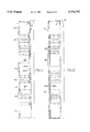
- FIG. 4 is an enlarged top plan view of the flexible substrate that forms part of the three dimensional flexible assembly of integrated circuits invention illustrated in FIGS. 2 and 3, but in its unfolded state;
- FIG. 5 is an enlarged bottom plan view of the unfolded flexible substrate that forms part of the three dimensional flexible assembly of integrated circuits invention illustrated in FIGS. 2, 3 and 4;
- FIG. 6 is an enlarged sectional view similar to that in FIG. 3 but of another embodiment of the three dimensional flexible assembly of integrated circuits invention with encapsulation rather than a cover;
- FIG. 7 is a sectional view similar to that in FIG. 3 but of another embodiment of the three dimensional flexible assembly of integrated circuits invention.
- FIG. 8 is a top plan view of the unfolded flexible substrate of the integrated circuit invention set forth in FIG. 7 with portions broken away for ease of illustration;
- FIG. 9 is a bottom plan view of the unfolded flexible substrate set forth in FIG. 8 with portions broken away for ease of illustration;
- FIG. 10 is a sectional view similar to that in FIG. 3 but of another embodiment of the three dimensional flexible assembly of integrated circuits invention.
- FIG. 11 is a top plan view of the flexible substrate that forms part of the circuit invention set forth in FIG. 10, but in its unfolded state with portions broken away for ease of illustration;
- FIG. 12 is a bottom plan view of the unfolded flexible substrate set forth in FIG. 11 with portions broken away for ease of illustration;
- FIG. 13 is a block diagram view of the basic method of the invention.
- the present invention uses a technique for creating a three-dimensional packaging arrangement of back-to-back chips located on one or both sides of a flexible substrate as will be hereinafter described in detail.
- the circuit package 10 comprises a flexible primary substrate 12 which is generally rectangular in shape and has an outer surface 14 and an oppositely located inner surface 16.
- the flexible substrate 12 is made of a thin metallized film material known in the art.
- the circuit package invention 10 also comprises a plurality of identical electronic chips 18 that are connected to portions of the inner surface 16 by solder bumps or other electrically conductive material represented by the number 22.
- the circuit package 10 also comprises a plurality of electronic circuit chips 24 that are located adjacent to portions of the inner surface 16 and are electrically connected to these inner portions by the solder bumps or other electrically conductive material represented by the number 28.
- the chips 18 and the adjacently located chips 24 are connected in a back to back relationship by the adhesive 29 and 30 that is known in the art.
- the circuit package invention 10 also comprises encapsulating means for encapsulating at least some of the chips 18 and 24 that comprises an encapsulating compound known in the art that is designated by the number 32.
- the circuit package invention 10 also comprises a rigid package substrate 34 and means for electrically connecting the flexible substrate 12 to the rigid package substrate comprising the electrical solder or other electrically conductive material connections 36 as well as means for encapsulating these connections that comprises an encapsulating compound 38 known in the art.
- the primary flexible substrate 12 has respective metallized layers 40 and 42 that form the respective outer 14 and inner surfaces 16.
- the flexible substrate 12 is folded so that there are two outer loops 20a and 20b formed by the substrate 12 with the chips 18 and 24 located in a back to back relationship inside the adjacent substrate 12 portion.
- Vias such as those numbered 44, 46, 48, 49 and 50 are also provided in the substrate 12 to allow the interconnection of the various chips 18 and 24 and/or assist in the connection of one or more of these chips 18 and 24 to the flex interface pads which form an interconnection to the rigid package substrate 34.
- a generally rectangular shaped dished cover 52 is provided that has a central dished portion 54 that is sized and shaped to receive the combined folded flexible primary substrate 12 and the associated connected chips 18 and 24.
- the cover 52 has a flat flange 56 surrounding its outer periphery that is sized and shaped to match the outer upper flat surface 58 of the rigid package substrate 34. This flange 56 is secured to the outer surface 58 by means known in the art such as by gold-tin solder so that the dished portion 54 receives and surrounds the completed combined folded substrate 12 and chips 18 and 24 assembly.
- FIG. 4 A top plan view of the unfolded flexible substrate 12 is illustrated in FIG. 4 and a bottom plan view is illustrated in FIG. 5.
- the flexible substrate 12 has four sets of electrical connections for the chips 18 and 24 designated respectively by the numbers 60, 62, 64 and 66. It will be noted that the same portion of the flexible substrate 12 that has the electrical connections 64 also has a series of electrical connections designated generally by the number 68 which contain vias 49 (FIG. 3) that connect the pads shown in FIG. 4 to the directly opposite pads 69 shown in FIG. 5. The pads 69 are used to electrically connect the flexible substrate 12 to the rigid package substrate 34.
- the flexible substrate 12 also has electrical connections or electrical conductive paths such as those designated 70a and 70b on the side 16 and 70c and 70d on the side 14 that electrically connect various individual connectors of the groups of electrical connectors 60, 62, 64 and 66 and individual connectors of the electrical connectors 69 that are used to electrically connect the flexible substrate 12 to the rigid package substrate 34.
- the groups of electrical connectors 60, 62, 64 and 66 are not equally spaced on the flexible substrate 12. As illustrated, the portion or space 71 on the flexible substrate 12 between the electrical connector groups 62 and 64 is greater than the portion or spaces between the groups 60 and 62, and 64 and 66. This space or distance 71 is greater since that portion 71 of the flexible substrate 12 must span a distance greater than the thickness of that of four chips 18 and 24 as well as two thickness of flexible substrate 12 when the flexible substrate 12 is folded as illustrated in FIG. 3.
- FIG. 6 illustrates a cross sectional view of an additional embodiment of the circuit package invention 73 that is identical to the embodiment of the circuit package invention set forth in FIGS. 1 through 5, but without a rigid base or package substrate 34 and the cover 52.
- the combined folded primary substrate 12 and the associated chips 18 and 24 are encapsulated with an encapsulating molding means for encapsulating the combined folded flexible primary substrate 12 and the associated connected chips 18 and 24 that could include a polymer molding or casting compound 75 such as Plaskon SMT-B-1 epoxy molding compound available from Rohm and Haas Company, Philadelphia, Pa.
- the assembly of the combined folded primary substrate 12 and the associated chips 18 and 24 is encapsulated with the compound 75 on five sides, leaving a pad array side 77 of the circuit package invention 73 uncovered to allow attachment at the next assembly (not shown).
- a pad array 79 is located on the exposed side 77 that is not covered by the encapsulating compound 75.
- solder balls 81 may be attached by reflow to the underside 77 to form a ball grid array for the embodiment 73.
- FIG. 7 illustrates a cross sectional view, taken substantially at the same location as the view in FIG. 3, of another embodiment of the circuit package invention that is designated by the number 72 and is substantially similar to the previously described embodiment 10 illustrated in FIGS. 1 through 5, but with a few modifications.
- the circuit package invention 72 has basically all of the same components as the circuit package invention 10 including the circuit chips 18 and 24 and the rigid substrate 34.
- the flexible substrate 74 is longer than the previous flexible substrate 12 and is folded in a different manner.
- the circuit package 72 has two additional chips 76 and 78 that are identical to the respective previously described chips 18 and 24. As illustrated in FIG.
- the flexible substrate 74 is folded so that there are three outer loops 80a, 80b, and 80c formed by the folded flexible substrate 74 with the chips 76 and 78 being located in a back to back relationship and located in and connected to the inside portions of the flexible substrate 74 adjacent to the loop 80b and the chips 18 and 24 being located in a back to back relationship and connected to the inside portions of the flexible substrate 74 adjacent to the loops 80a and 80c.
- the circuit package invention 72 has its various chips 18, 24, and 76, 78 electrically connected to the flexible substrate 74 by solder bumps or other suitable electrically conductive material designated by the number 82.
- the chips 18 and 76, the adjacently located chips 24 and 78 are connected in back to back relationships by the adhesive 84, 86 and 88 that is known in the art.
- the flexible end portions 83 and 85 of the flexible substrate 74 are also connected to the adjacent portions of the flexible substrate 74 by the respective adhesive 87 and 89 that is known in the art.
- the end portions 83 and 85 of the flexible substrate 74 are located within or surrounded by other portions of the flexible substrate 74.
- the circuit package 72 also comprises encapsulating means 90 comprising an encapsulating compound known in the art for encapsulating at least some of the chips 18, 24, 76 and 78.
- the circuit package 72 also comprises means for electrically connecting the flexible substrate 74 to the rigid package substrate 34 comprising the electrical solder or other suitable electrically conductive material connections 92 and means for encapsulating the connections 92 comprising an encapsulating compound 94 known in the art.
- the circuit package 72 also has a generally rectangular shaped dished cover 95 that is similar to the previously described cover 52 for the embodiment 10 illustrated in FIGS. 1 through 3.
- the cover 95 has a deeper dished portion 97 than the dished portion 54 of the cover 52 and the deeper dished portion 97 is sized and shaped to receive the added volume of the longer folded substrate 74 and the associated chips 18, 24, 76 and 78.
- FIGS. 8 and 9 illustrate respectively top and a bottom plan views of the unfolded flexible substrate 74 illustrated in FIG. 7.
- the flexible substrate 74 has four sets of electrical connections for the chips 18 and 24 on its upper surface 63 that are designated generally by the numbers 96, 98, 100 and 102.
- the same portion of the flexible substrate 74 that has the electrical connections 100 also has a series of electrical connections designated generally by the number 104 which contain vias (not shown) that electrically connect the pads shown in FIG. 8 to the directly opposite pads 105 shown in FIG. 9.
- the pads 105 electrically connect the flexible substrate 74 to the rigid substrate 34.
- FIG. 8 illustrates respectively top and a bottom plan views of the unfolded flexible substrate 74 illustrated in FIG. 7.
- the flexible substrate 74 has four sets of electrical connections for the chips 18 and 24 on its upper surface 63 that are designated generally by the numbers 96, 98, 100 and 102.
- the same portion of the flexible substrate 74 that has the electrical connections 100 also has a series of electrical connections designated generally
- the other side 67 of the flexible substrate 74 has two sets of electrical connections for the chips 76 and 78 that are designated by the numbers 106 and 108.
- the flexible substrate 74 also has electrical connections or electrically conductive paths 110a and 110b on the side 63 and 110c and 110d on the side 67 that electrically connect various individual connectors of the groups of electrical connectors 96, 98, 100, 102, 106 and 108 and individual connectors of the electrical connectors 105 that are used to connect the flexible substrate 74 to the rigid substrate 34.
- the flexible substrate 74 set forth in FIGS. 8 and 9 has groups of electrical connectors 96, 98, 100, 102, 106 and 108 that are not all equally spaced on the flexible substrate 74.
- the space or flexible substrate portion 112 between the group of electrical connectors 98 and 100 is significantly greater than the other spaces or substrate portions between the other groups of electrical connectors 106, 108, 96, 98, 100 and 102.
- This portion 112 is greater since this portion 112 must span a distance greater than the thickness of a total six chips 18, 24, 76 and 78 plus four thicknesses of flexible substrate 74 when the flexible substrate 74 is folded as illustrated in FIG. 7.
- FIG. 10 illustrates a cross sectional view of another embodiment of the circuit package invention that is designated by the number 114 and is substantially similar to the previously described embodiments 10 and 72 with a few modifications.
- the circuit package invention 114 has basically all of the same components of the previously described circuit package invention 72 including the circuit chips 18, 24, 76 and 78 and the rigid substrate 34.
- the circuit package invention 114 has a longer flexible substrate 116 than the previously described flexible substrate 74 and it is also folded in a different manner. As illustrated in FIG. 10, the circuit package 114 has two additional circuit chips 118 and 120 that are identical to the previously described circuit chips 18, 24, 76 and 78.
- the flexible substrate 116 is folded so that there are four outer loops 122a, 122b, 122c and 122d formed by the folded flexible substrate 116 with the respective chips 18, 24; 118, 120; 76, 78 and 24, 18 located in a back to back relationship and connected to the inside portions of the flexible substrate 116 adjacent to the respective loops 122a, 122b, 122c and 122d.
- the circuit package 114 has its various chips 18, 24, 76, 78 118 and 120 electrically connected to the flexible substrate 116 by the solder or other suitable electrically conductive material bumps designated by the number 124.
- the chips 18, 76, and 118 and the adjacently located chips 24, 78 and 120 are connected in back to back relationship by the adhesive 126, 128, 130 and 132 that is known in the art. It is important to note that the end portions 133 and 135 of the flexible substrate 116 are located within or surrounded by other portions of the flexible substrate 116. The flexible end portions 133 and 135 of the flexible substrate 116 are also connected to the adjacent portions of the flexible substrate 116 by the adhesive 137 and 139, and portions of the flexible substrate 116 are also connected together by the adhesive 141 that is known in the art.
- the circuit package 114 also comprises encapsulating means 134 comprising an encapsulating compound known in the art for encapsulating at least some of the chips 18, 24, 76, 78, 118 and 120.
- the circuit package 114 also comprises means for electrically connecting the flexible substrate 116 to the rigid substrate 34 comprising the electrical solder or other suitable electrically conductive material connections 136 and means for encapsulating the solder connections 136 comprising an encapsulating compound 138 known in the art.
- the circuit package 114 also has a generally rectangular shaped dished cover 143 that is similar to the previously described cover 52 for the embodiment 10 illustrated in FIGS. 1 through 3 and the cover 95 for the embodiment 72 illustrated in FIG. 7.
- the cover 143 has a deeper dished portion 145 than the dished portion 54 of the cover 52 or the dished portion 97 of the cover 95 and the deeper dished portion 145 is sized and shaped to receive the added volume of the longer folded substrate 116 and the associated chips 18, 24, 76, 78, 118 and 120.
- FIGS. 11 and 12 illustrate respectively top and bottom plan views of the unfolded flexible substrate 116 illustrated in FIG. 10.
- the flexible substrate 116 has six sets of electrical connections for chips 18, 24, 118 and 120 located on its upper surface 117 that are designated generally by the numbers 140, 142, 144, 146, 148 and 150.
- the same portion of the flexible substrate 116 that has the set of electrical connections 148 also has a series of electrical connections designated generally by the number 152 which contain vias (not shown) that connect the pads shown in FIG. 11 to the directly opposite pads 153 shown in FIG. 12.
- the pads 153 electrically connect the flexible substrate 116 to the rigid substrate 34.
- FIG. 11 illustrates the flexible substrate 116 to the rigid substrate 34.
- the other side 119 of the flexible substrate 116 has two sets of electrical connections for the chips 76 and 78 that are designated by the numbers 154 and 156.
- the flexible substrate 116 also has electrical connections or electrically conductive paths 158a and 158b on the side 117 and 158c and 158d on the side 119 that electrically interconnect various individual connectors of the groups of electrical connectors 140, 142, 144, 146, 148, 150, 154, and 156 and individual connectors of the electrical connectors 153 that are used to connect the flexible substrate 116 to the rigid substrate 34.
- the flexible substrate 116 as illustrated in FIGS. 11 and 12 has a larger distance or portion 160 between the group of electrical connectors 146 and 148 as well as a somewhat smaller greater distance portion 162 located adjacent to the group of electrical connectors 144.
- These larger portions 160 and 162 are needed since they respectively span a distance greater than the thickness of eight chips 18, 24, 76, 78, 118 and 120 plus six thickness of flexible substrate 116 in the case of the portion 160 and the thickness of four chips 76, 78, 118 and 120 plus three thickness of flexible substrate 116 in the case of the portion 162 when the flexible substrate 116 is folded as illustrated in FIG. 10.
- a flexible substrate having electrical connections for chips at specific locations such as that designated 12 in FIG. 4, is provided.
- chips that are to be electrically connected to the flexible substrate such as chips 18 and 24 in FIG. 3, are provided.
- chips 18 and 24 are then electrically connected to the respective electrical connections 60, 62, 64 and 66 on the flexible substrate 12.
- the bond pads of the chips 18 and 24 are bumped with conductive material such as tin-lead solder or conductive polymer adhesive or other suitable electrically conductive material using conventional, known flip-chip bumping techniques.
- Each of the four chips 18 and 24 is attached using known flip-chip mounting techniques to the flexible substrate 12 as shown in FIG. 3.
- the bond pad area on a chip 18 or 24 typically has a bond pad pitch in the range of 0.004-0.020 of an inch.
- a chip bond pad pitch of 0.010 of an inch or less is too small for compatibility with cofired or conventional printed wiring design rules. Larger pitches allow higher yield assembly using stencil printed solder paste and solder reflow.
- existing chip bond patterns are reconfigured using a flexible substrate 12 as shown in FIGS. 2, 3, 4 and 5.
- Flexible printed circuit technology allows formation of the fine pitch bond patterns and interconnect tracks required for interface with integrated circuit chips.
- the flexible substrate 12 has connections on two layers. The primary side 16 layer interfaces and performs an electrical coupling with four functional chips 18 and 24 using conventional flip-chip interconnection with known bumping and assembly techniques.
- the conductive interface pattern comprises an array of conductive pads with bond pads similar in size to those on the chip. Typical chip bond pad size of 0.002-0.006 of an inch and the corresponding chip interface bond pads are the same or within 0.004 of being the same size.
- a secondary array of substrate interface pads 69 is located on the side 14 opposite the connections 64 to create an array with a larger bond pad pitch and pad diameter. Suitable patterns may have a pitch within the range of 0.010-0.100 of an inch.
- a pad pattern that mirrors the package substrate pattern is provided on the secondary side 15 for electrical conductive material attachment using material such as solder, conductive adhesive or other suitable electrically conductive material interconnection to a substrate.
- Interconnect tracks are provided on either or both sides of the flexible substrate 12 to connect the chip bond pad patterns to the rigid substrate interface bond pad pattern as indicated in FIG. 4. Vias, such as those designated by the numbers 44, 46, 48, 49 and 50 as illustrated in FIG. 3, are located in the bond pad patterns to provide connections between the sides 14 and 16 of the flexible substrate 12. In making the connections, the external layer surfaces of the copper conductors are finished using known metalization techniques with gold, tin, or tin-lead at the locations for attachment of the chips and at the attachment pads for assembly to the package substrate 34.
- a low viscosity epoxy adhesive material 32 is applied along one or two edges of each chip 18 and 24 to fill the space between the flexible substrate 12 and the opposing chip 18 and 24 face by capillary action which draws the applied material into the space between the chip and the flexible substrate 12.
- the expansion characteristic desired for this material 32 is that it be closely matched to the conductive interface material expansion.
- This encapsulating resin 32 provides rigid support for the thin, flexible substrate 12 circuit material and maintains planarity of the interface pads which are to be attached to a substrate at the next level of assembly. This resin also improves fatigue life of the connections when the package is exposed to temperature cycling. The material is cured to form a rigidized assembly with the flexible substrate 12 unfolded.
- each chip 18 and 24 is connected and rigidized to the flexible substrate 12, the assembly is folded into the arrangement illustrated in FIGS. 2 and 3 with the end portions 23 and 25 of the flexible substrate 12 positioned inside the folded assembly so that they are surrounded by a portion of the flexible substrate 12. Then the backs of the two pairs of chips 18 and 24 which face each other and the opposing flex substrate portions 33A and 33B are bonded together with a liquid epoxy or film epoxy material, such as that designated by the numbers 29, 30 and 31 in FIG. 3, to form a bonded stack. This stack is then ready to be attached to a package substrate such as that designated 34.
- the package substrate 34 may be formed of any material suitable for electronic packaging including, but not limited to, alumina, aluminum nitride, silicon, mullite, glass-ceramic, or aramid fiber reinforced polyimide or epoxy. A material possessing low expansion characteristics (3-10 ppm/degree Celsius) which nearly matches the expansion characteristic of the silicon chip, may be desired to improve the long term reliability of the flip-chip connections under a cyclic temperature environment.
- the upward facing surface 35 of the package substrate 34 is dedicated to interface and perform an electrical coupling with the flexible circuit of the stacked chip assembly. This surface 35 is formed in a conventional manner and located for attachment of the flexible circuit chip stack using land grid array or ball grid array techniques. A second interface pattern is provided on the downward facing substrate layer 37. This pattern is used to interface with a matching pattern used for the next higher level assembly.
- this rigid package substrate 34 is provided and the chips 18 and 24 and flexible substrate 12 assembly is then assembled to the rigid package substrate 34 by using conventional known surface mount assembly connection techniques.
- solder paste is stencil printed to the substrate 34 bond pad pattern, and the chips 18 and 24 and flexible substrate 12 assembly is placed in the solder paste, and the assembly is reflowed to form the solder connections 36.
- solder may be introduced as plated solder on the package substrate 34 or flexible substrate 12 or solder preforms may be used. Any other conductive material such as conductive polymer adhesive may also be used in a similar manner in place of the solder paste.
- a low expansion, low modulus epoxy resin 38 is provided and this epoxy resin 38 is inserted into the space between the rigid substrate 34 and the flexible substrate 12 so that this space is filled with a rigid, low expansion, low modulus epoxy resin 38 after solder reflow (or conductive polymer cure) connection of the flexible substrate 12 and associated chips 18 and 24 to the rigid substrate 34.
- the rigid substrate 34 is optional.
- a cover 52 is then provided and the cover 52 is placed over and around the stacked folded flexible substrate 12 and chips 18 and 24 assembly and secured to the rigid substrate 34 to close out the package in order to provide a sealed enclosure. If desired this cover 52 can be omitted such as in cases where environments that require a sealed enclosure are not anticipated.
- the combined folded primary substrate 12 and the associated chips 18 and 24 can be encapsulated with encapsulating means that could include a polymer molding or casting compound such as Plaskon SMT-B-1 epoxy molding compound 75 that was referred to previously.
- the assembly of the combined folded primary 12 substrate and the associated chips 18 and 24 is encapsulated with the compound 75 on five sides, leaving the pad array side 77 of the circuit package invention 73 uncovered to allow attachment at the next assembly (not shown) by the pad array 79 that is located on the exposed side 77 that is not covered by the encapsulating compound 75.
- solder balls 81 may be attached by reflow to the underside 77 to form a ball grid array for the embodiment 73.
- the basic method of manufacturing the integrated circuit package invention comprises the steps of first providing a flexible substrate having end portions with electrical connections for chips 164, providing a plurality of chips having a back 166, and then connecting the plurality of chips to the electrical connections located on the flexible substrate 168.
- the method of manufacturing an integrated circuit package invention then includes the steps of folding the flexible substrate in such a manner that said chips have their backs located adjacent to the back of another chip and folding the flexible substrate in such a manner to cause the end portions to be located within or surrounded by other portions of said flexible substrate 170, connecting the backs of the adjacently located chips together to form a combined flexible substrate and chips assembly 172, providing a rigid substrate having electrical connections 174, and electrically connecting the combined flexible substrate and chips assembly to the rigid substrate 176.
- the last two steps 174 and 176 are optional.
- the method of manufacturing an integrated circuit module or package assembly can also comprise, after the step of electrically connecting the combined flexible substrate and chips assembly to the rigid substrate 176 set forth above, the steps of providing a cover, such as the cover 52 in FIGS. 1 through 3, for covering the combined flexible substrate and chips assembly and covering the combined flexible substrate and chips assembly with the cover.
- the method of manufacturing an integrated circuit can further comprise the steps of providing an adhesive material such as that designated 32 in FIG. 3, and applying the adhesive material between each chip 18 and 24 and the adjacent surface of the flexible substrate 12 after the step of connecting the plurality of chips to the electrical connections located on the flexible substrate 168 indicated in FIG. 13.
- the method of manufacturing an integrated circuit package can include the additional steps of providing an encapsulating compound, such as the compound 38 in FIG. 3, and filling the space between the rigid substrate 34 and the adjacently located combined flexible substrate and chips assembly with the encapsulating compound 38 after the step of electrically connecting the combined flexible substrate and chips assembly to the rigid substrate 176 indicated in FIG. 13.
- an encapsulating compound such as the compound 38 in FIG. 3
- the above indicated method can be implemented in a leaded or leadless ceramic package. This approach can be used with four chips or up to any reasonable even number, such as the six and eight stacked assembly of chips illustrated respectively in FIGS. 7 and 10.
- the cover 52 and the rigid base substrate 34 can be omitted.
- the method would omit the step of providing a rigid substrate having electrical connections 174 and the step of electrically connecting the combined flexible substrate and chips assembly to the rigid substrate 176 as well as the steps of providing a cover 52 for covering the combined flexible substrate and chips assembly and covering the combined folded flexible substrate and chips assembly with the cover 52.
- the method would substitute the following steps of providing an encapsulating compound 75 for encapsulating the combined flexible substrate and chips assembly and encapsulating the combined flexible substrate and chips assembly with the encapsulating compound 75 for encapsulating the combined flexible substrate and chips assembly for the steps referred to above that were omitted. This will result in the the circuit package invention 73 set forth in FIG. 6 where the encapsulating compound 75 is illustrated.
- the assembled circuit package invention 10 as well as the other embodiments 73, 72 and 114 can then be used in a conventional manner. However, due to the high density of chips, the embodiments of the invention 10, 73, 72 and 114 are suitable for use in many applications where other circuit packaging techniques would not work.
Abstract
A three dimensional flexible assembly of integrated circuits and method of fabricating the assembly of circuits including a folded flexible substrate with integrated circuit chips. The invention has provisions for allowing mechanical and electrically functional attachment of integrated circuit chips to one or both sides of the flexible substrate using flip chip assembly techniques. In addition, a rigid package substrate is provided upon which the folded substrate is secured with the associated chips. The chips are electrically connected to the flexible substrate and the flexible substrate is in turn electrically connected to the rigid substrate. A cover is also provided that covers and protects the flexible substrate and the associated chips as well as a portion of the connected rigid package substrate. In an additional embodiment, the cover and rigid substrate are omitted and instead the combined folded flexible substrate and integrated circuit chips are encapsulated with a suitable compound.
Description
This is a divisional patent application of co-pending U.S. patent application Ser. No. 08/577,843 filed Dec. 22, 1995 that has been allowed, now U.S. Pat. No. 5,646,446.
The increased complexity of spacecraft and aircraft as well as other vehicles has resulted in a need to incorporate more and more electronic systems in such vehicles. However, the complexity has reached a point where the required and desired electronic systems exceed the available space in the vehicle to accept all such systems. In order to overcome this problem, numerous efforts have and are being made to reduce the size of the electronic packages that make up such electronic systems.
Electronic system evolution has followed the trend of producing more functionality in less volume, at lower weight, and lower cost. Improvements in integrated circuit chip density and functionality have mostly contributed toward improved efficiency, however, advancements in packaging of these devices have also been beneficial. As it becomes more difficult to achieve substantial improvements through integrated circuit technology advances, new packaging approaches have become necessary to obtain density improvements and to allow the full performance potential of interconnected chips to be used. The term "chip" in this description refers to an electrically functional integrated circuit die. The active face of the chip is defined as the surface on which the integrated electronics have been disposed. The back side refers to the surface opposite the active face.
It is known to place an integrated circuit chip in a ceramic or plastic package for protection and then solder the package to a substrate. Typical integrated circuit packages contain only one chip. The package is substantially larger than the chip, thereby limiting the overall packaging density. Conventional packaging systems employing printed circuit boards with single chip packages are unable to provide the required number of chips within a volume and weight which is compatible with the needs of advanced circuit applications.
Applications which require large memory capacity suffer from excessive packaging overhead when single chip packages are used. The present invention relates to integrated circuitry packaging to increase its functional density, through use of a three-dimensional assembly arrangement, and to reduce material and assembly costs.
This invention includes the use of a folded flexible substrate with chips contained on one or both sides of the substrate. The techniques of this invention are applicable for use with any form of commercially available memory chip.
A three dimensional integrated circuit assembly is provided comprising a folded flexible substrate with integrated circuit chips and means for allowing mechanical and electrically functional attachment of integrated circuit chips to one or both sides of the flexible substrate using flip chip assembly techniques. The folded stack of chips and flexible assembly is encapsulated with a polymer molding compound or cast polymer material. The assembly is encapsulated on five sides leaving the pad array side of the stacked chips and flexible circuit assembly uncovered to allow attachment to the next assembly.
In addition, a package substrate is provided upon which the folded substrate is secured with the associated chips. The chips are electrically connected to the flexible substrate and the flexible substrate is in turn electrically connected to the rigid package substrate. A cover is also provided that covers and protects the flexible substrate and the associated chips as well as a portion of the connected rigid package substrate.
This invention provides a method of disposing integrated circuits in a vertical stack which then interfaces with a substrate. The interface area is similar size to that required to ordinarily interface a single integrated circuit chip with a substrate. This invention provides a method for interconnecting two or more chips to a flexible circuit made of a thin, metallized film material. The assembled flexible circuit is folded such that a n-high stack of chips is achieved where n is the number of chips attached to the flexible circuit. Any reasonable number of chips can be assembled in this manner. This creates a three-dimensional arrangement of chips for more effective use of substrate area and allows more chips to be contained in a given volume.
Thus, there is provided a ceramic, or other low expansion substrate material, with a means for allowing mechanical and electrically functional attachment of a stack of chips to the substrate using land grid array or ball grid array assembly techniques. A land grid array is formed with an array of conductive bond pads, circular, square or other suitable shape, formed on two opposing substrates. The two opposing patterns are connected together using solder (conductive adhesive or any other suitable conductive material) thus forming an electrical and mechanical connection. A ball grid array is similar except that balls of appropriate size and of a non-melting, but solder wettable (or adhesive bondable material) are included in the pad array so as to increase and control the spacing between the two opposing substrates. The substrate additionally provides an interconnect method for these stacked chips by means of internal vias and circuitry. The circuit packages described herein increase the density (volumetric efficiency) over existing approaches in order to provide higher density, lower weight, and improved functional performance for electronic systems.
This invention relates to the packaging of electronic circuits and more particularly to the packaging of electronic circuitry that uses less volume.
Accordingly, it is an object of the invention to provide an electronic circuit package and method that result in reduced volume and lower cost.
It is an object of the invention to provide an electronic circuit package and method that are capable of being used with a wide number of integrated circuits.
It is an object of the invention to provide an integrated circuit package and method that provide increased functionality with reduced volume.
It is an object of the invention to provide an integrated circuit package and method that result in increased functional density.
It is an object of the invention to provide an integrated circuit package and method that are well suited for use in circuits where the volume available for the circuit is limited.
It is an object of the invention to provide an integrated circuit package and method that are well suited for use in a variety of difficult situations.
It is an object of the invention to provide an integrated circuit package and method that permit multiple integrated circuits to be packaged in the same size of package that would contain fewer integrated circuit chips.
It is an object of the invention to provide an integrated circuit package and method that produce a compact package.
It is an object of the invention to provide an integrated circuit package and method that use bonded back to back mounted chips.
It is an object of the invention to provide an integrated circuit package and method in which the ends of the substrate are buried within the integrated circuit package.
It is an object of the invention to provide an integrated circuit package and method that produce a compact package where four or more chips can take up the space of only one chip.
It is an object of the invention to provide an integrated circuit package and method that produce a multiple chip package which can be handled as if it were a single chip.
It is an object of the invention to provide an integrated circuit package and method that are adapted for use with a wide variety of available chips.
It is an object of the invention to provide an integrated circuit package and method that are adapted for use with any form of commercially available chip.
It is also an object of the invention to provide an integrated circuit package and method that create a three dimensional assembly of c hips.
It is an object of the invention to provide an integrated circuit package and method that allow additional use of the space above or below a flexible substrate.
It is an object of the invention to provide an integrated circuit package and method that effectively increase the packaging density by many times over existing packaging techniques.
It is an object of the invention to provide an integrated circuit package assembly and method that include special means for mounting, stacking, and functionally interconnecting chips so as to provide increased functional density.
It is also an object of the present invention to provide an integrated circuit package and method that result in attaching integrated circuits to a substrate to optimize package and chip density.
It is another object of the invention to provide an integrated circuit package and method that use novel packaging technology to provide a high density package for chips that is useful for a variety of applications.
It is still another object of this invention is to provide an integrated package and method which are suitable for use with standard commercial chips of various dimensions.
It is a further object of this invention to provide an integrated circuit package and method that efficiently interconnect the chips in a high density package.
It is an object of the invention to provide an integrated circuit package and method where the multiple chip package can be mounted in a manner similar to a single flip chip combination.
It is an object of the invention to provide an integrated circuit package and method where the package can be mounted using a land grid array pattern.
It is an object of the invention to provide an integrated circuit package and method where the package can be mounted using distributed pads.
It is an object of the invention to provide an integrated circuit package and method where the stack pad array uses larger than normal pads.
It is an object of the invention to provide an integrated circuit package and method where the stack pad array uses a greater than normal pitch between pads.
It is an object of the invention to provide an integrated circuit package and method that uses chip underfill to rigidize the flexible substrate.
It is an object of the invention to provide an integrated circuit package and method whereby the chip stack is encapsulated by injection molding or by cast polymer material.
It is an object of the invention to provide an integrated circuit package and method that do not require an additional substrate.
These and other objects of the invention will be apparent from the three dimensional flexible assembly of integrated circuits invention that includes a folded flexible substrate with integrated circuit chips and means for allowing mechanical and electrically functional attachment of integrated circuit chips to one or both sides of the flexible substrate using flip chip assembly techniques. In addition, a package substrate is provided upon which the folded substrate is secured with the associated chips. The chips are electrically connected to the flexible substrate and the flexible substrate is in turn electrically connected to the rigid package substrate. A cover is also provided that covers and protects the flexible substrate and the associated chips as well as a portion of the connected rigid package substrate. However, the cover and rigid package substrate can be omitted if such protection is not necessary or desired.
The method of the invention includes: 1) providing a flexible substrate with electrical connections for chips; 2) providing chips to be connected to the electrical connections on the electrical substrate; 3) connecting the chips to the electrical connections on the flexible substrate; 4) providing a low viscosity adhesive material and then injecting this material under each chip to fill the space between the surface of the chips and the adjacent flexible substrate surface; 5) folding the flexible substrate with the chips connected to it in such a manner that the chips are located in a back to back relationship; 6) connecting the chips together in a back to back relationship to form a stacked assembly of chips and a folded substrate; 7) providing a rigid package substrate with electrical connections; 8) connecting the stacked assembly of chips and a folded substrate to the electrical connections on the rigid package substrate; 9) providing a cover having provisions for receiving the stacked assembly of chips and flexible substrate and securing the cover to the rigid package substrate.
The invention will be hereinafter more fully described with references to the accompanying drawings in which:
FIG. 1 is a perspective view of the three dimensional flexible assembly of integrated circuits invention;
FIG. 2 is an exploded perspective view of the three dimensional flexible assembly of integrated circuits invention illustrated in FIG. 1;
FIG. 3 is an enlarged sectional view of the three dimensional flexible assembly of integrated circuits invention taken substantially on the line 3--3 of FIG. 1;
FIG. 4 is an enlarged top plan view of the flexible substrate that forms part of the three dimensional flexible assembly of integrated circuits invention illustrated in FIGS. 2 and 3, but in its unfolded state;
FIG. 5 is an enlarged bottom plan view of the unfolded flexible substrate that forms part of the three dimensional flexible assembly of integrated circuits invention illustrated in FIGS. 2, 3 and 4;
FIG. 6 is an enlarged sectional view similar to that in FIG. 3 but of another embodiment of the three dimensional flexible assembly of integrated circuits invention with encapsulation rather than a cover;
FIG. 7 is a sectional view similar to that in FIG. 3 but of another embodiment of the three dimensional flexible assembly of integrated circuits invention;
FIG. 8 is a top plan view of the unfolded flexible substrate of the integrated circuit invention set forth in FIG. 7 with portions broken away for ease of illustration;
FIG. 9 is a bottom plan view of the unfolded flexible substrate set forth in FIG. 8 with portions broken away for ease of illustration;
FIG. 10 is a sectional view similar to that in FIG. 3 but of another embodiment of the three dimensional flexible assembly of integrated circuits invention;
FIG. 11 is a top plan view of the flexible substrate that forms part of the circuit invention set forth in FIG. 10, but in its unfolded state with portions broken away for ease of illustration;
FIG. 12 is a bottom plan view of the unfolded flexible substrate set forth in FIG. 11 with portions broken away for ease of illustration; and
FIG. 13 is a block diagram view of the basic method of the invention.
Many of the techniques disclosed in this detailed description of the invention are exemplary only, and it should be clear to one skilled in the art that alternate techniques may be employed in practicing this invention. Further, other techniques which are peripheral to the invention and well known in the art, such as how to fabricate a flexible printed wiring substrate, or ceramic substrate, are not disclosed so as to prevent obscuring the invention in unnecessary detail.
In order to increase the density of current substrates using integrated circuit chips, the present invention uses a technique for creating a three-dimensional packaging arrangement of back-to-back chips located on one or both sides of a flexible substrate as will be hereinafter described in detail.
Referring first to FIGS. 1, 2 and 3 the circuit package invention is illustrated and is designated by the number 10. The circuit package 10 comprises a flexible primary substrate 12 which is generally rectangular in shape and has an outer surface 14 and an oppositely located inner surface 16. The flexible substrate 12 is made of a thin metallized film material known in the art. The circuit package invention 10 also comprises a plurality of identical electronic chips 18 that are connected to portions of the inner surface 16 by solder bumps or other electrically conductive material represented by the number 22.
The circuit package 10 also comprises a plurality of electronic circuit chips 24 that are located adjacent to portions of the inner surface 16 and are electrically connected to these inner portions by the solder bumps or other electrically conductive material represented by the number 28. The chips 18 and the adjacently located chips 24 are connected in a back to back relationship by the adhesive 29 and 30 that is known in the art. The circuit package invention 10 also comprises encapsulating means for encapsulating at least some of the chips 18 and 24 that comprises an encapsulating compound known in the art that is designated by the number 32. The circuit package invention 10 also comprises a rigid package substrate 34 and means for electrically connecting the flexible substrate 12 to the rigid package substrate comprising the electrical solder or other electrically conductive material connections 36 as well as means for encapsulating these connections that comprises an encapsulating compound 38 known in the art.
It will be noted that the primary flexible substrate 12 has respective metallized layers 40 and 42 that form the respective outer 14 and inner surfaces 16. In addition, as illustrated in FIG. 3, the flexible substrate 12 is folded so that there are two outer loops 20a and 20b formed by the substrate 12 with the chips 18 and 24 located in a back to back relationship inside the adjacent substrate 12 portion. Vias such as those numbered 44, 46, 48, 49 and 50 are also provided in the substrate 12 to allow the interconnection of the various chips 18 and 24 and/or assist in the connection of one or more of these chips 18 and 24 to the flex interface pads which form an interconnection to the rigid package substrate 34. It is important to note that the end portions 23 and 25 of the flexible substrate 12 are connected together by the adhesive 31 and that they are located within or surrounded by other portions of the flexible substrate 12. Also, as illustrated, a generally rectangular shaped dished cover 52 is provided that has a central dished portion 54 that is sized and shaped to receive the combined folded flexible primary substrate 12 and the associated connected chips 18 and 24. The cover 52 has a flat flange 56 surrounding its outer periphery that is sized and shaped to match the outer upper flat surface 58 of the rigid package substrate 34. This flange 56 is secured to the outer surface 58 by means known in the art such as by gold-tin solder so that the dished portion 54 receives and surrounds the completed combined folded substrate 12 and chips 18 and 24 assembly.
A top plan view of the unfolded flexible substrate 12 is illustrated in FIG. 4 and a bottom plan view is illustrated in FIG. 5. As illustrated in FIG. 4, the flexible substrate 12 has four sets of electrical connections for the chips 18 and 24 designated respectively by the numbers 60, 62, 64 and 66. It will be noted that the same portion of the flexible substrate 12 that has the electrical connections 64 also has a series of electrical connections designated generally by the number 68 which contain vias 49 (FIG. 3) that connect the pads shown in FIG. 4 to the directly opposite pads 69 shown in FIG. 5. The pads 69 are used to electrically connect the flexible substrate 12 to the rigid package substrate 34. As illustrated, the flexible substrate 12 also has electrical connections or electrical conductive paths such as those designated 70a and 70b on the side 16 and 70c and 70d on the side 14 that electrically connect various individual connectors of the groups of electrical connectors 60, 62, 64 and 66 and individual connectors of the electrical connectors 69 that are used to electrically connect the flexible substrate 12 to the rigid package substrate 34.
It should be noted that the groups of electrical connectors 60, 62, 64 and 66, though they are substantially identical, are not equally spaced on the flexible substrate 12. As illustrated, the portion or space 71 on the flexible substrate 12 between the electrical connector groups 62 and 64 is greater than the portion or spaces between the groups 60 and 62, and 64 and 66. This space or distance 71 is greater since that portion 71 of the flexible substrate 12 must span a distance greater than the thickness of that of four chips 18 and 24 as well as two thickness of flexible substrate 12 when the flexible substrate 12 is folded as illustrated in FIG. 3.
FIG. 6 illustrates a cross sectional view of an additional embodiment of the circuit package invention 73 that is identical to the embodiment of the circuit package invention set forth in FIGS. 1 through 5, but without a rigid base or package substrate 34 and the cover 52. Instead of the rigid substrate 34 and cover 52, the combined folded primary substrate 12 and the associated chips 18 and 24 are encapsulated with an encapsulating molding means for encapsulating the combined folded flexible primary substrate 12 and the associated connected chips 18 and 24 that could include a polymer molding or casting compound 75 such as Plaskon SMT-B-1 epoxy molding compound available from Rohm and Haas Company, Philadelphia, Pa. The assembly of the combined folded primary substrate 12 and the associated chips 18 and 24 is encapsulated with the compound 75 on five sides, leaving a pad array side 77 of the circuit package invention 73 uncovered to allow attachment at the next assembly (not shown). A pad array 79 is located on the exposed side 77 that is not covered by the encapsulating compound 75. Optionally, solder balls 81 may be attached by reflow to the underside 77 to form a ball grid array for the embodiment 73.
FIG. 7 illustrates a cross sectional view, taken substantially at the same location as the view in FIG. 3, of another embodiment of the circuit package invention that is designated by the number 72 and is substantially similar to the previously described embodiment 10 illustrated in FIGS. 1 through 5, but with a few modifications. The circuit package invention 72 has basically all of the same components as the circuit package invention 10 including the circuit chips 18 and 24 and the rigid substrate 34. However, the flexible substrate 74 is longer than the previous flexible substrate 12 and is folded in a different manner. In addition, the circuit package 72 has two additional chips 76 and 78 that are identical to the respective previously described chips 18 and 24. As illustrated in FIG. 7, the flexible substrate 74 is folded so that there are three outer loops 80a, 80b, and 80c formed by the folded flexible substrate 74 with the chips 76 and 78 being located in a back to back relationship and located in and connected to the inside portions of the flexible substrate 74 adjacent to the loop 80b and the chips 18 and 24 being located in a back to back relationship and connected to the inside portions of the flexible substrate 74 adjacent to the loops 80a and 80c.
The circuit package invention 72 has its various chips 18, 24, and 76, 78 electrically connected to the flexible substrate 74 by solder bumps or other suitable electrically conductive material designated by the number 82. In addition, the chips 18 and 76, the adjacently located chips 24 and 78 are connected in back to back relationships by the adhesive 84, 86 and 88 that is known in the art. The flexible end portions 83 and 85 of the flexible substrate 74 are also connected to the adjacent portions of the flexible substrate 74 by the respective adhesive 87 and 89 that is known in the art. Also, in a manner similar to that illustrated in FIG. 3 for the embodiment 10, the end portions 83 and 85 of the flexible substrate 74 are located within or surrounded by other portions of the flexible substrate 74. The circuit package 72 also comprises encapsulating means 90 comprising an encapsulating compound known in the art for encapsulating at least some of the chips 18, 24, 76 and 78. The circuit package 72 also comprises means for electrically connecting the flexible substrate 74 to the rigid package substrate 34 comprising the electrical solder or other suitable electrically conductive material connections 92 and means for encapsulating the connections 92 comprising an encapsulating compound 94 known in the art. The circuit package 72 also has a generally rectangular shaped dished cover 95 that is similar to the previously described cover 52 for the embodiment 10 illustrated in FIGS. 1 through 3. However, the cover 95 has a deeper dished portion 97 than the dished portion 54 of the cover 52 and the deeper dished portion 97 is sized and shaped to receive the added volume of the longer folded substrate 74 and the associated chips 18, 24, 76 and 78.
FIGS. 8 and 9 illustrate respectively top and a bottom plan views of the unfolded flexible substrate 74 illustrated in FIG. 7. As illustrated in FIG. 8, the flexible substrate 74 has four sets of electrical connections for the chips 18 and 24 on its upper surface 63 that are designated generally by the numbers 96, 98, 100 and 102. Also, as illustrated, the same portion of the flexible substrate 74 that has the electrical connections 100 also has a series of electrical connections designated generally by the number 104 which contain vias (not shown) that electrically connect the pads shown in FIG. 8 to the directly opposite pads 105 shown in FIG. 9. The pads 105 electrically connect the flexible substrate 74 to the rigid substrate 34. In addition, as illustrated in FIG. 9, the other side 67 of the flexible substrate 74 has two sets of electrical connections for the chips 76 and 78 that are designated by the numbers 106 and 108. The flexible substrate 74 also has electrical connections or electrically conductive paths 110a and 110b on the side 63 and 110c and 110d on the side 67 that electrically connect various individual connectors of the groups of electrical connectors 96, 98, 100, 102, 106 and 108 and individual connectors of the electrical connectors 105 that are used to connect the flexible substrate 74 to the rigid substrate 34.
As was the case with the previously described flexible substrate 12 illustrated in FIG. 4 and 5, the flexible substrate 74 set forth in FIGS. 8 and 9 has groups of electrical connectors 96, 98, 100, 102, 106 and 108 that are not all equally spaced on the flexible substrate 74. Specifically, the space or flexible substrate portion 112 between the group of electrical connectors 98 and 100 is significantly greater than the other spaces or substrate portions between the other groups of electrical connectors 106, 108, 96, 98, 100 and 102. This portion 112 is greater since this portion 112 must span a distance greater than the thickness of a total six chips 18, 24, 76 and 78 plus four thicknesses of flexible substrate 74 when the flexible substrate 74 is folded as illustrated in FIG. 7.
FIG. 10 illustrates a cross sectional view of another embodiment of the circuit package invention that is designated by the number 114 and is substantially similar to the previously described embodiments 10 and 72 with a few modifications. The circuit package invention 114 has basically all of the same components of the previously described circuit package invention 72 including the circuit chips 18, 24, 76 and 78 and the rigid substrate 34. The circuit package invention 114 has a longer flexible substrate 116 than the previously described flexible substrate 74 and it is also folded in a different manner. As illustrated in FIG. 10, the circuit package 114 has two additional circuit chips 118 and 120 that are identical to the previously described circuit chips 18, 24, 76 and 78.
The flexible substrate 116 is folded so that there are four outer loops 122a, 122b, 122c and 122d formed by the folded flexible substrate 116 with the respective chips 18, 24; 118, 120; 76, 78 and 24, 18 located in a back to back relationship and connected to the inside portions of the flexible substrate 116 adjacent to the respective loops 122a, 122b, 122c and 122d. The circuit package 114 has its various chips 18, 24, 76, 78 118 and 120 electrically connected to the flexible substrate 116 by the solder or other suitable electrically conductive material bumps designated by the number 124. In addition, the chips 18, 76, and 118 and the adjacently located chips 24, 78 and 120 are connected in back to back relationship by the adhesive 126, 128, 130 and 132 that is known in the art. It is important to note that the end portions 133 and 135 of the flexible substrate 116 are located within or surrounded by other portions of the flexible substrate 116. The flexible end portions 133 and 135 of the flexible substrate 116 are also connected to the adjacent portions of the flexible substrate 116 by the adhesive 137 and 139, and portions of the flexible substrate 116 are also connected together by the adhesive 141 that is known in the art. In addition, the circuit package 114 also comprises encapsulating means 134 comprising an encapsulating compound known in the art for encapsulating at least some of the chips 18, 24, 76, 78, 118 and 120. The circuit package 114 also comprises means for electrically connecting the flexible substrate 116 to the rigid substrate 34 comprising the electrical solder or other suitable electrically conductive material connections 136 and means for encapsulating the solder connections 136 comprising an encapsulating compound 138 known in the art. The circuit package 114 also has a generally rectangular shaped dished cover 143 that is similar to the previously described cover 52 for the embodiment 10 illustrated in FIGS. 1 through 3 and the cover 95 for the embodiment 72 illustrated in FIG. 7. However, the cover 143 has a deeper dished portion 145 than the dished portion 54 of the cover 52 or the dished portion 97 of the cover 95 and the deeper dished portion 145 is sized and shaped to receive the added volume of the longer folded substrate 116 and the associated chips 18, 24, 76, 78, 118 and 120.
FIGS. 11 and 12 illustrate respectively top and bottom plan views of the unfolded flexible substrate 116 illustrated in FIG. 10. As illustrated in FIG. 11, the flexible substrate 116 has six sets of electrical connections for chips 18, 24, 118 and 120 located on its upper surface 117 that are designated generally by the numbers 140, 142, 144, 146, 148 and 150. Also, the same portion of the flexible substrate 116 that has the set of electrical connections 148 also has a series of electrical connections designated generally by the number 152 which contain vias (not shown) that connect the pads shown in FIG. 11 to the directly opposite pads 153 shown in FIG. 12. The pads 153 electrically connect the flexible substrate 116 to the rigid substrate 34. In addition, as illustrated in FIG. 12, the other side 119 of the flexible substrate 116 has two sets of electrical connections for the chips 76 and 78 that are designated by the numbers 154 and 156. The flexible substrate 116 also has electrical connections or electrically conductive paths 158a and 158b on the side 117 and 158c and 158d on the side 119 that electrically interconnect various individual connectors of the groups of electrical connectors 140, 142, 144, 146, 148, 150, 154, and 156 and individual connectors of the electrical connectors 153 that are used to connect the flexible substrate 116 to the rigid substrate 34.
In a manner similar to that for the previously described flexible substrates 12 and 74, that have the respective larger spaces 71 and 112, the flexible substrate 116 as illustrated in FIGS. 11 and 12 has a larger distance or portion 160 between the group of electrical connectors 146 and 148 as well as a somewhat smaller greater distance portion 162 located adjacent to the group of electrical connectors 144. These larger portions 160 and 162 are needed since they respectively span a distance greater than the thickness of eight chips 18, 24, 76, 78, 118 and 120 plus six thickness of flexible substrate 116 in the case of the portion 160 and the thickness of four chips 76, 78, 118 and 120 plus three thickness of flexible substrate 116 in the case of the portion 162 when the flexible substrate 116 is folded as illustrated in FIG. 10.
The method of the invention as well as the manner of manufacturing or forming the integrated circuit package or the three dimensional flexible assembly of integrated circuits invention illustrated in the figures is set forth below using the embodiment of the invention 10 which is for a four chip hermetic leadless package as illustrated in FIGS. 1 through 5 or the modified embodiment set forth in FIG. 6. First, a flexible substrate having electrical connections for chips at specific locations, such as that designated 12 in FIG. 4, is provided. Also, chips that are to be electrically connected to the flexible substrate, such as chips 18 and 24 in FIG. 3, are provided. Four chips 18 and 24 are then electrically connected to the respective electrical connections 60, 62, 64 and 66 on the flexible substrate 12. In accomplishing this, the bond pads of the chips 18 and 24 are bumped with conductive material such as tin-lead solder or conductive polymer adhesive or other suitable electrically conductive material using conventional, known flip-chip bumping techniques.
Each of the four chips 18 and 24 is attached using known flip-chip mounting techniques to the flexible substrate 12 as shown in FIG. 3. The bond pad area on a chip 18 or 24 typically has a bond pad pitch in the range of 0.004-0.020 of an inch. A chip bond pad pitch of 0.010 of an inch or less is too small for compatibility with cofired or conventional printed wiring design rules. Larger pitches allow higher yield assembly using stencil printed solder paste and solder reflow. In this invention, existing chip bond patterns are reconfigured using a flexible substrate 12 as shown in FIGS. 2, 3, 4 and 5. Flexible printed circuit technology allows formation of the fine pitch bond patterns and interconnect tracks required for interface with integrated circuit chips. The flexible substrate 12 has connections on two layers. The primary side 16 layer interfaces and performs an electrical coupling with four functional chips 18 and 24 using conventional flip-chip interconnection with known bumping and assembly techniques.
The conductive interface pattern comprises an array of conductive pads with bond pads similar in size to those on the chip. Typical chip bond pad size of 0.002-0.006 of an inch and the corresponding chip interface bond pads are the same or within 0.004 of being the same size. In addition, a secondary array of substrate interface pads 69 is located on the side 14 opposite the connections 64 to create an array with a larger bond pad pitch and pad diameter. Suitable patterns may have a pitch within the range of 0.010-0.100 of an inch. A pad pattern that mirrors the package substrate pattern is provided on the secondary side 15 for electrical conductive material attachment using material such as solder, conductive adhesive or other suitable electrically conductive material interconnection to a substrate. Interconnect tracks are provided on either or both sides of the flexible substrate 12 to connect the chip bond pad patterns to the rigid substrate interface bond pad pattern as indicated in FIG. 4. Vias, such as those designated by the numbers 44, 46, 48, 49 and 50 as illustrated in FIG. 3, are located in the bond pad patterns to provide connections between the sides 14 and 16 of the flexible substrate 12. In making the connections, the external layer surfaces of the copper conductors are finished using known metalization techniques with gold, tin, or tin-lead at the locations for attachment of the chips and at the attachment pads for assembly to the package substrate 34.
After attachment of the chips 18 and 24 using flip-chip mounting techniques, as indicated previously, a low viscosity epoxy adhesive material 32 is applied along one or two edges of each chip 18 and 24 to fill the space between the flexible substrate 12 and the opposing chip 18 and 24 face by capillary action which draws the applied material into the space between the chip and the flexible substrate 12. The expansion characteristic desired for this material 32 is that it be closely matched to the conductive interface material expansion. This encapsulating resin 32 provides rigid support for the thin, flexible substrate 12 circuit material and maintains planarity of the interface pads which are to be attached to a substrate at the next level of assembly. This resin also improves fatigue life of the connections when the package is exposed to temperature cycling. The material is cured to form a rigidized assembly with the flexible substrate 12 unfolded.
After each chip 18 and 24 is connected and rigidized to the flexible substrate 12, the assembly is folded into the arrangement illustrated in FIGS. 2 and 3 with the end portions 23 and 25 of the flexible substrate 12 positioned inside the folded assembly so that they are surrounded by a portion of the flexible substrate 12. Then the backs of the two pairs of chips 18 and 24 which face each other and the opposing flex substrate portions 33A and 33B are bonded together with a liquid epoxy or film epoxy material, such as that designated by the numbers 29, 30 and 31 in FIG. 3, to form a bonded stack. This stack is then ready to be attached to a package substrate such as that designated 34.
The known multi-layer approach for fabricating a printed wiring substrate or co-fired ceramic substrate is extended by adding appropriate circuitry layers. The package substrate 34 may be formed of any material suitable for electronic packaging including, but not limited to, alumina, aluminum nitride, silicon, mullite, glass-ceramic, or aramid fiber reinforced polyimide or epoxy. A material possessing low expansion characteristics (3-10 ppm/degree Celsius) which nearly matches the expansion characteristic of the silicon chip, may be desired to improve the long term reliability of the flip-chip connections under a cyclic temperature environment. The upward facing surface 35 of the package substrate 34 is dedicated to interface and perform an electrical coupling with the flexible circuit of the stacked chip assembly. This surface 35 is formed in a conventional manner and located for attachment of the flexible circuit chip stack using land grid array or ball grid array techniques. A second interface pattern is provided on the downward facing substrate layer 37. This pattern is used to interface with a matching pattern used for the next higher level assembly.
With the method this rigid package substrate 34 is provided and the chips 18 and 24 and flexible substrate 12 assembly is then assembled to the rigid package substrate 34 by using conventional known surface mount assembly connection techniques. For example, solder paste is stencil printed to the substrate 34 bond pad pattern, and the chips 18 and 24 and flexible substrate 12 assembly is placed in the solder paste, and the assembly is reflowed to form the solder connections 36. Alternatively, solder may be introduced as plated solder on the package substrate 34 or flexible substrate 12 or solder preforms may be used. Any other conductive material such as conductive polymer adhesive may also be used in a similar manner in place of the solder paste.
As an option, a low expansion, low modulus epoxy resin 38 is provided and this epoxy resin 38 is inserted into the space between the rigid substrate 34 and the flexible substrate 12 so that this space is filled with a rigid, low expansion, low modulus epoxy resin 38 after solder reflow (or conductive polymer cure) connection of the flexible substrate 12 and associated chips 18 and 24 to the rigid substrate 34. However, the rigid substrate 34 is optional.
A cover 52 is then provided and the cover 52 is placed over and around the stacked folded flexible substrate 12 and chips 18 and 24 assembly and secured to the rigid substrate 34 to close out the package in order to provide a sealed enclosure. If desired this cover 52 can be omitted such as in cases where environments that require a sealed enclosure are not anticipated.
As an alternative to a cover 52 and a base substrate 34 as indicated and described previously in connection with FIG. 6, the combined folded primary substrate 12 and the associated chips 18 and 24 can be encapsulated with encapsulating means that could include a polymer molding or casting compound such as Plaskon SMT-B-1 epoxy molding compound 75 that was referred to previously. The assembly of the combined folded primary 12 substrate and the associated chips 18 and 24 is encapsulated with the compound 75 on five sides, leaving the pad array side 77 of the circuit package invention 73 uncovered to allow attachment at the next assembly (not shown) by the pad array 79 that is located on the exposed side 77 that is not covered by the encapsulating compound 75. Optionally, solder balls 81 may be attached by reflow to the underside 77 to form a ball grid array for the embodiment 73.
From the foregoing and as indicated in FIG. 13, the basic method of manufacturing the integrated circuit package invention comprises the steps of first providing a flexible substrate having end portions with electrical connections for chips 164, providing a plurality of chips having a back 166, and then connecting the plurality of chips to the electrical connections located on the flexible substrate 168. The method of manufacturing an integrated circuit package invention then includes the steps of folding the flexible substrate in such a manner that said chips have their backs located adjacent to the back of another chip and folding the flexible substrate in such a manner to cause the end portions to be located within or surrounded by other portions of said flexible substrate 170, connecting the backs of the adjacently located chips together to form a combined flexible substrate and chips assembly 172, providing a rigid substrate having electrical connections 174, and electrically connecting the combined flexible substrate and chips assembly to the rigid substrate 176. However, the last two steps 174 and 176 are optional.
The method of manufacturing an integrated circuit module or package assembly can also comprise, after the step of electrically connecting the combined flexible substrate and chips assembly to the rigid substrate 176 set forth above, the steps of providing a cover, such as the cover 52 in FIGS. 1 through 3, for covering the combined flexible substrate and chips assembly and covering the combined flexible substrate and chips assembly with the cover.
Additionally, the method of manufacturing an integrated circuit can further comprise the steps of providing an adhesive material such as that designated 32 in FIG. 3, and applying the adhesive material between each chip 18 and 24 and the adjacent surface of the flexible substrate 12 after the step of connecting the plurality of chips to the electrical connections located on the flexible substrate 168 indicated in FIG. 13.
Also, the method of manufacturing an integrated circuit package can include the additional steps of providing an encapsulating compound, such as the compound 38 in FIG. 3, and filling the space between the rigid substrate 34 and the adjacently located combined flexible substrate and chips assembly with the encapsulating compound 38 after the step of electrically connecting the combined flexible substrate and chips assembly to the rigid substrate 176 indicated in FIG. 13.
The above indicated method can be implemented in a leaded or leadless ceramic package. This approach can be used with four chips or up to any reasonable even number, such as the six and eight stacked assembly of chips illustrated respectively in FIGS. 7 and 10.
As an alternative, if a non-hermetic package is acceptable, the cover 52 and the rigid base substrate 34 can be omitted. In this case the method would omit the step of providing a rigid substrate having electrical connections 174 and the step of electrically connecting the combined flexible substrate and chips assembly to the rigid substrate 176 as well as the steps of providing a cover 52 for covering the combined flexible substrate and chips assembly and covering the combined folded flexible substrate and chips assembly with the cover 52. Instead, the method would substitute the following steps of providing an encapsulating compound 75 for encapsulating the combined flexible substrate and chips assembly and encapsulating the combined flexible substrate and chips assembly with the encapsulating compound 75 for encapsulating the combined flexible substrate and chips assembly for the steps referred to above that were omitted. This will result in the the circuit package invention 73 set forth in FIG. 6 where the encapsulating compound 75 is illustrated.
The assembled circuit package invention 10 as well as the other embodiments 73, 72 and 114 can then be used in a conventional manner. However, due to the high density of chips, the embodiments of the invention 10, 73, 72 and 114 are suitable for use in many applications where other circuit packaging techniques would not work.
Although the invention has been described in considerable detail with reference to certain preferred embodiments, it will be appreciated and understood that various changes and modifications may be made without departing from the spirit and scope of the invention as defined in the appended claims.
Claims (6)
1. A method of manufacturing an integrated circuit package comprising the steps of:
A. providing a flexible substrate with electrical connections for chips and having end portions;
B. providing a plurality of chips having a back;
C. connecting said plurality of chips to the electrical connections located on said flexible substrate;
D. folding said flexible substrate in such a manner that said chips have their backs located adjacent to the back of another chip and end portions are located within or surrounded by other portions of said flexible substrate; and
E. connecting the backs of said adjacently located chips together to form a combined flexible substrate and chips assembly.
2. The method of manufacturing an integrated circuit of claim 1 further comprising the following steps after the step of connecting the backs of said adjacently located chips together to form a combined flexible substrate and chips assembly: providing a rigid substrate having electrical connections; and electrically connecting said combined flexible substrate and chips assembly to said rigid substrate.
3. The method of manufacturing an integrated circuit of claim 2 further comprising the following steps after the step of electrically connecting said combined flexible substrate and chips assembly to said rigid substrate: providing a cover for covering said combined flexible substrate and chip assembly and covering said combined flexible substrate and chip assembly with said cover.
4. The method of manufacturing an integrated circuit of claim 3 further comprising the steps of providing an adhesive material, and applying said adhesive material between each chip and the adjacent surface of said flexible substrate after the step of connecting the plurality of chips to the electrical connections located on the flexible substrate.
5. The method of manufacturing an integrated circuit of claim 4 including the additional steps of providing an encapsulating compound and filling the space between said rigid substrate and said adjacently located combined flexible substrate and chip assembly with said encapsulating compound.
6. The method of manufacturing an integrated circuit of claim 1 further comprising the following steps after the step of connecting the backs of said adjacently located chips together to form a combined flexible substrate and chips assembly: providing an encapsulating compound and encapsulating said combined flexible substrate and chips assembly with said encapsulating compound.
Priority Applications (1)
| Application Number | Priority Date | Filing Date | Title |
|---|---|---|---|
| US08/887,430 US5776797A (en) | 1995-12-22 | 1997-07-02 | Three-dimensional flexible assembly of integrated circuits |
Applications Claiming Priority (2)
| Application Number | Priority Date | Filing Date | Title |
|---|---|---|---|
| US08/577,843 US5646446A (en) | 1995-12-22 | 1995-12-22 | Three-dimensional flexible assembly of integrated circuits |
| US08/887,430 US5776797A (en) | 1995-12-22 | 1997-07-02 | Three-dimensional flexible assembly of integrated circuits |
Related Parent Applications (1)
| Application Number | Title | Priority Date | Filing Date |
|---|---|---|---|
| US08/577,843 Division US5646446A (en) | 1995-12-22 | 1995-12-22 | Three-dimensional flexible assembly of integrated circuits |
Publications (1)
| Publication Number | Publication Date |
|---|---|
| US5776797A true US5776797A (en) | 1998-07-07 |
Family
ID=24310377
Family Applications (2)
| Application Number | Title | Priority Date | Filing Date |
|---|---|---|---|
| US08/577,843 Expired - Fee Related US5646446A (en) | 1995-12-22 | 1995-12-22 | Three-dimensional flexible assembly of integrated circuits |
| US08/887,430 Expired - Fee Related US5776797A (en) | 1995-12-22 | 1997-07-02 | Three-dimensional flexible assembly of integrated circuits |
Family Applications Before (1)
| Application Number | Title | Priority Date | Filing Date |
|---|---|---|---|
| US08/577,843 Expired - Fee Related US5646446A (en) | 1995-12-22 | 1995-12-22 | Three-dimensional flexible assembly of integrated circuits |
Country Status (1)
| Country | Link |
|---|---|
| US (2) | US5646446A (en) |
Cited By (155)
| Publication number | Priority date | Publication date | Assignee | Title |
|---|---|---|---|---|
| WO1999018607A1 (en) * | 1997-10-03 | 1999-04-15 | The Board Of Trustees Of The University Of Arkansas | Methods of making flexible substrates for electronic packaging and flexible substrates formed by the method |
| WO1999065282A1 (en) * | 1998-06-10 | 1999-12-16 | Irvine Sensors Corporation | Ic stack utilizing flexible circuits with bga contacts |
| US6028365A (en) * | 1998-03-30 | 2000-02-22 | Micron Technology, Inc. | Integrated circuit package and method of fabrication |
| US6121676A (en) * | 1996-12-13 | 2000-09-19 | Tessera, Inc. | Stacked microelectronic assembly and method therefor |
| US6225688B1 (en) | 1997-12-11 | 2001-05-01 | Tessera, Inc. | Stacked microelectronic assembly and method therefor |
| US20010003049A1 (en) * | 1996-07-12 | 2001-06-07 | Norio Fukasawa | Method and mold for manufacturing semiconductor device, semiconductor device, and method for mounting the device |
| US6252299B1 (en) * | 1997-09-29 | 2001-06-26 | Hitachi, Ltd. | Stacked semiconductor device including improved lead frame arrangement |
| US6262895B1 (en) * | 2000-01-13 | 2001-07-17 | John A. Forthun | Stackable chip package with flex carrier |
| US20010026388A1 (en) * | 2000-02-08 | 2001-10-04 | Framatome Connectors International | Electro-optical connector module |
| US6300679B1 (en) * | 1998-06-01 | 2001-10-09 | Semiconductor Components Industries, Llc | Flexible substrate for packaging a semiconductor component |
| US6310392B1 (en) * | 1998-12-28 | 2001-10-30 | Staktek Group, L.P. | Stacked micro ball grid array packages |
| US6337225B1 (en) * | 2000-03-30 | 2002-01-08 | Advanced Micro Devices, Inc. | Method of making stacked die assemblies and modules |
| WO2002009182A1 (en) * | 2000-07-25 | 2002-01-31 | 3D Plus | Method for distributed shielding and/or bypass for electronic device with three-dimensional interconnection |
| WO2002049109A1 (en) * | 2000-12-11 | 2002-06-20 | Medtronic, Inc. | Stacked die package |
| US6417027B1 (en) * | 1999-06-10 | 2002-07-09 | Micron Technology, Inc. | High density stackable and flexible substrate-based devices and systems and methods of fabricating |
| US20020164838A1 (en) * | 2001-05-02 | 2002-11-07 | Moon Ow Chee | Flexible ball grid array chip scale packages and methods of fabrication |
| US20020190367A1 (en) * | 2001-06-15 | 2002-12-19 | Mantz Frank E. | Slice interconnect structure |
| US20030002267A1 (en) * | 2001-06-15 | 2003-01-02 | Mantz Frank E. | I/O interface structure |
| US20030025211A1 (en) * | 2001-07-24 | 2003-02-06 | Ted Bruce | Chip stack with differing chip package types |
| US20030048624A1 (en) * | 2001-08-22 | 2003-03-13 | Tessera, Inc. | Low-height multi-component assemblies |
| US20030051911A1 (en) * | 2001-09-20 | 2003-03-20 | Roeters Glen E. | Post in ring interconnect using 3-D stacking |
| WO2002060527A3 (en) * | 2000-12-26 | 2003-03-27 | Medtronic Inc | Implantable medical electronics using high voltage flip chip components |
| US6552910B1 (en) * | 2000-06-28 | 2003-04-22 | Micron Technology, Inc. | Stacked-die assemblies with a plurality of microelectronic devices and methods of manufacture |
| US20030081392A1 (en) * | 2001-10-26 | 2003-05-01 | Staktek Group, L.P. | Integrated circuit stacking system and method |
| US6560117B2 (en) * | 2000-06-28 | 2003-05-06 | Micron Technology, Inc. | Packaged microelectronic die assemblies and methods of manufacture |
| US6573461B2 (en) | 2001-09-20 | 2003-06-03 | Dpac Technologies Corp | Retaining ring interconnect used for 3-D stacking |
| US6576992B1 (en) | 2001-10-26 | 2003-06-10 | Staktek Group L.P. | Chip scale stacking system and method |
| US6600222B1 (en) * | 2002-07-17 | 2003-07-29 | Intel Corporation | Stacked microelectronic packages |
| US6605869B2 (en) * | 2001-04-03 | 2003-08-12 | Nec Electronics Corporation | Semiconductor device with improved cooling efficiency and reduced electric resistance |
| US6607937B1 (en) | 2000-08-23 | 2003-08-19 | Micron Technology, Inc. | Stacked microelectronic dies and methods for stacking microelectronic dies |
| US20030164551A1 (en) * | 2002-03-04 | 2003-09-04 | Lee Teck Kheng | Method and apparatus for flip-chip packaging providing testing capability |
| US20030168725A1 (en) * | 1996-12-13 | 2003-09-11 | Tessera, Inc. | Methods of making microelectronic assemblies including folded substrates |
| US6658296B1 (en) | 2001-06-19 | 2003-12-02 | Pacesetter, Inc. | Implantable cardioverter defibrillator having an articulated flexible circuit element and method of manufacturing |
| US20030232085A1 (en) * | 1999-01-08 | 2003-12-18 | Emisphere Technologies, Inc. | Polymeric delivery agents and delivery agent compounds |
| US20030234443A1 (en) * | 2001-10-26 | 2003-12-25 | Staktek Group, L.P. | Low profile stacking system and method |
| US6670700B1 (en) * | 1999-08-19 | 2003-12-30 | Seiko Epson Corporation | Interconnect substrate and semiconductor device electronic instrument |
| US20040000708A1 (en) * | 2001-10-26 | 2004-01-01 | Staktek Group, L.P. | Memory expansion and chip scale stacking system and method |
| US6677670B2 (en) * | 2000-04-25 | 2004-01-13 | Seiko Epson Corporation | Semiconductor device |
| US20040052060A1 (en) * | 2001-10-26 | 2004-03-18 | Staktek Group, L.P. | Low profile chip scale stacking system and method |
| WO2004025699A2 (en) * | 2002-09-11 | 2004-03-25 | Tessera, Inc. | Assemblies having stacked semiconductor chips |
| US6717250B1 (en) * | 1999-10-20 | 2004-04-06 | Seiko Epson Corporation | Stacked semiconductor apparatus and electronic device including stacked semiconductor apparatus |
| US20040090845A1 (en) * | 2001-03-07 | 2004-05-13 | Hewlett-Packard Company | Fabrication and assembly structures and methods for memory devices |
| US20040099938A1 (en) * | 2002-09-11 | 2004-05-27 | Tessera, Inc. | Assemblies having stacked semiconductor chips and methods of making same |
| US20040108584A1 (en) * | 2002-12-05 | 2004-06-10 | Roeters Glen E. | Thin scale outline package |
| US20040115866A1 (en) * | 2002-09-06 | 2004-06-17 | Tessera, Inc. | Methods of making microelectronic packages including folded substrates |
| US20040124527A1 (en) * | 2002-12-31 | 2004-07-01 | Chia-Pin Chiu | Folded BGA package design with shortened communication paths and more electrical routing flexibility |
| US20040126050A1 (en) * | 2002-12-30 | 2004-07-01 | Claydon Glenn Scott | Assembly, contact and coupling interconnection for optoelectronics |
| US6765288B2 (en) | 2002-08-05 | 2004-07-20 | Tessera, Inc. | Microelectronic adaptors, assemblies and methods |
| US20040145052A1 (en) * | 2003-01-29 | 2004-07-29 | Matsushita Electric Industrial Co., Ltd. | Semiconductor device and display device using the same |
| US20040150946A1 (en) * | 2001-10-02 | 2004-08-05 | International Business Machines Corporation | Electronic units and method for packaging and assembly of said electronic units |
| US20040150107A1 (en) * | 2002-12-31 | 2004-08-05 | Cha Ki Bon | Stack package and fabricating method thereof |
| US20040157365A1 (en) * | 2002-12-30 | 2004-08-12 | Koh Kyung Hee | Method for packaging a multi-chip module of a semiconductor device |
| US20040164396A1 (en) * | 1999-08-19 | 2004-08-26 | Seiko Epson Corporation | Interconnect substrate and method of manufacture thereof, electronic component and method of manufacturing thereof, circuit board and electronic instrument |
| US20040183183A1 (en) * | 2001-10-26 | 2004-09-23 | Staktek Group, L.P. | Integrated circuit stacking system and method |
| US20040191442A1 (en) * | 2003-03-27 | 2004-09-30 | Florencia Lim | Surface modification of expanded ultra high molecular weight polyethylene (eUHMWPE) for improved bondability |
| US20040209400A1 (en) * | 2002-08-26 | 2004-10-21 | Meyers John G. | Process and apparatus for packaging a tape substrate |
| US20040207990A1 (en) * | 2003-04-21 | 2004-10-21 | Rose Andrew C. | Stair-step signal routing |
| US20040238931A1 (en) * | 2003-05-30 | 2004-12-02 | Tessera, Inc. | Assemblies having stacked semiconductor chips and methods of making same |
| US20040251557A1 (en) * | 2003-06-16 | 2004-12-16 | Sandisk Corporation | Integrated circuit package having stacked integrated circuits and method therefor |
| US20050012199A1 (en) * | 2003-07-18 | 2005-01-20 | Rosenau Steven A. | Folded flex circuit interconnect having a grid array interface |
| US20050012194A1 (en) * | 2003-07-17 | 2005-01-20 | Jaeck Edward W. | Electronic package having a folded package substrate |
| US20050019984A1 (en) * | 2000-08-09 | 2005-01-27 | Tongbi Jiang | Multiple substrate microelectronic devices and methods of manufacture |
| US6881611B1 (en) * | 1996-07-12 | 2005-04-19 | Fujitsu Limited | Method and mold for manufacturing semiconductor device, semiconductor device and method for mounting the device |
| US20050150813A1 (en) * | 2003-10-29 | 2005-07-14 | Tessera, Inc. | Foldover packages and manufacturing and test methods therefor |
| SG112807A1 (en) * | 2001-08-31 | 2005-07-28 | Micron Technology Inc | Packaged microelectronic die assemblies and methods of manufacture |
| US20050167817A1 (en) * | 2002-08-05 | 2005-08-04 | Tessera, Inc. | Microelectronic adaptors, assemblies and methods |
| US20050174748A1 (en) * | 2004-01-14 | 2005-08-11 | Denso Corporation | Electronic control device |
| WO2005104227A1 (en) * | 2004-04-20 | 2005-11-03 | Staktek Group L.P. | Stacked module systems and methods |
| US20050279916A1 (en) * | 2004-05-03 | 2005-12-22 | Tessera, Inc. | Image sensor package and fabrication method |
| US6984881B2 (en) | 2003-06-16 | 2006-01-10 | Sandisk Corporation | Stackable integrated circuit package and method therefor |
| US20060033217A1 (en) * | 2004-08-10 | 2006-02-16 | Brian Taggart | Flip-chips on flex substrates, flip-chip and wire-bonded chip stacks, and methods of assembling same |
| US7030488B2 (en) * | 2001-10-30 | 2006-04-18 | Intel Corporation | Packaged combination memory for electronic devices |
| US20060086453A1 (en) * | 2002-07-08 | 2006-04-27 | Dela Cruz Ernesto S | Forming folded-stack packaged device using vertical progression folding tool |
| US7053478B2 (en) * | 2001-10-26 | 2006-05-30 | Staktek Group L.P. | Pitch change and chip scale stacking system |
| US7067352B1 (en) * | 2004-03-08 | 2006-06-27 | David Ralph Scheid | Vertical integrated package apparatus and method |
| WO2005112100A3 (en) * | 2004-04-30 | 2006-08-24 | Staktek Group Lp | Stacked module systems and methods |
| KR100618542B1 (en) * | 1999-07-27 | 2006-08-31 | 삼성전자주식회사 | Method for manufacturing stack package |
| US20060243392A1 (en) * | 2002-09-30 | 2006-11-02 | Pieda Ruel B | Forming folded-stack packaged device using progressive folding tool |
| US7132754B1 (en) * | 2005-03-17 | 2006-11-07 | Alfred E. Mann Foundation For Scientific Research | Flip chip stack |
| US20060261458A1 (en) * | 2003-11-12 | 2006-11-23 | Amkor Technology, Inc. | Semiconductor package and manufacturing method thereof |
| US20060267173A1 (en) * | 2005-05-26 | 2006-11-30 | Sandisk Corporation | Integrated circuit package having stacked integrated circuits and method therefor |
| US20060286717A1 (en) * | 2005-05-06 | 2006-12-21 | Tessera, Inc. | Stacked microelectronic assemblies having basal compliant layers |
| US7154171B1 (en) * | 2002-02-22 | 2006-12-26 | Amkor Technology, Inc. | Stacking structure for semiconductor devices using a folded over flexible substrate and method therefor |
| KR100675729B1 (en) * | 2000-10-18 | 2007-02-01 | 삼성전자주식회사 | Stack package using flexible substrate |
| US20070040251A1 (en) * | 2004-01-12 | 2007-02-22 | Alvin Seah | Method for connecting a die assembly to a substrate in an integrated circuit and a semiconductor device comprising a die assembly |
| US20070059918A1 (en) * | 2005-09-14 | 2007-03-15 | Samsung Electro-Mechanics Co., Ltd. | Rigid-flexible printed circuit board for package on package and manufacturing method |
| US20070074907A1 (en) * | 2003-09-16 | 2007-04-05 | Koninklijke Philips Electronics N.V. | Method of manufacturing an electronic device and an electronic device |
| US7202555B2 (en) * | 2001-10-26 | 2007-04-10 | Staktek Group L.P. | Pitch change and chip scale stacking system and method |
| EP1780664A2 (en) * | 1998-11-30 | 2007-05-02 | Hitachi, Ltd. | Method of mounting electronic circuit chip |
| US20070164428A1 (en) * | 2006-01-18 | 2007-07-19 | Alan Elbanhawy | High power module with open frame package |
| US20070187807A1 (en) * | 2006-02-13 | 2007-08-16 | Jeongil Lee | Multi-chip module for battery power control |
| US20070235886A1 (en) * | 2006-04-06 | 2007-10-11 | Hamza Yilmaz | Semiconductor die packages using thin dies and metal substrates |
| US20080001279A1 (en) * | 2006-06-30 | 2008-01-03 | Alan Elbanhawy | Chip module for complete power train |
| US20080054417A1 (en) * | 2006-08-29 | 2008-03-06 | Sangdo Lee | Semiconductor die package including stacked dice and heat sink structures |
| US20080086173A1 (en) * | 2006-08-18 | 2008-04-10 | Jerry Ok | Package for an Implantable Neural Stimulation Device |
| US20080122113A1 (en) * | 2006-08-17 | 2008-05-29 | Corisis David J | Semiconductor device assemblies and systems including at least one conductive pathway extending around a side of at least one semiconductor device and methods for forming the same |
| US20080185696A1 (en) * | 2007-02-05 | 2008-08-07 | Ruben Madrid | Semiconductor die package including leadframe with die attach pad with folded edge |
| US20080217762A1 (en) * | 2007-03-09 | 2008-09-11 | Phoenix Precision Technology Corporation | Chip carrier structure having semiconductor chip embedded therein and metal layer formed thereon |
| US7425758B2 (en) | 2006-08-28 | 2008-09-16 | Micron Technology, Inc. | Metal core foldover package structures |
| US20080251739A1 (en) * | 2007-04-13 | 2008-10-16 | Yoon Hwa Choi | Optical coupler package |
| US20080258272A1 (en) * | 2007-04-19 | 2008-10-23 | Lay Yeap Lim | Etched leadframe structure |
| US7485951B2 (en) * | 2001-10-26 | 2009-02-03 | Entorian Technologies, Lp | Modularized die stacking system and method |
| US20090057852A1 (en) * | 2007-08-27 | 2009-03-05 | Madrid Ruben P | Thermally enhanced thin semiconductor package |
| US20090057854A1 (en) * | 2007-08-28 | 2009-03-05 | Gomez Jocel P | Self locking and aligning clip structure for semiconductor die package |
| US20090057855A1 (en) * | 2007-08-30 | 2009-03-05 | Maria Clemens Quinones | Semiconductor die package including stand off structures |
| US20090109636A1 (en) * | 2007-10-25 | 2009-04-30 | Chipstack, Inc. | Multiple package module using a rigid flex printed circuit board |
| US20090140266A1 (en) * | 2007-11-30 | 2009-06-04 | Yong Liu | Package including oriented devices |
| US20090140179A1 (en) * | 2007-11-30 | 2009-06-04 | Yong Liu | Semiconductor die packages suitable for optoelectronic applications having clip attach structures for angled mounting of dice |
| US20090160036A1 (en) * | 2007-12-19 | 2009-06-25 | David Grey | Package with multiple dies |
| US20090174044A1 (en) * | 2007-12-13 | 2009-07-09 | Eom Joo-Yang | Multi-chip package |
| US20090174048A1 (en) * | 2008-01-09 | 2009-07-09 | Yong Liu | Die package including substrate with molded device |
| US20090179313A1 (en) * | 2008-01-10 | 2009-07-16 | Maria Clemens Quinones | Flex clip connector for semiconductor device |
| US20090194856A1 (en) * | 2008-02-06 | 2009-08-06 | Gomez Jocel P | Molded package assembly |
| US20090218666A1 (en) * | 2008-02-28 | 2009-09-03 | Yang Gwi-Gyeon | Power device package and method of fabricating the same |
| US20090230536A1 (en) * | 2008-03-12 | 2009-09-17 | Yong Liu | Semiconductor die package including multiple semiconductor dice |
| US20090243079A1 (en) * | 2008-03-31 | 2009-10-01 | Lim Seung-Won | Semiconductor device package |
| US20090278241A1 (en) * | 2008-05-08 | 2009-11-12 | Yong Liu | Semiconductor die package including die stacked on premolded substrate including die |
| US7656678B2 (en) | 2001-10-26 | 2010-02-02 | Entorian Technologies, Lp | Stacked module systems |
| US7719098B2 (en) | 2001-10-26 | 2010-05-18 | Entorian Technologies Lp | Stacked modules and method |
| US7737549B2 (en) | 2004-09-03 | 2010-06-15 | Entorian Technologies Lp | Circuit module with thermal casing systems |
| US20100148346A1 (en) * | 2008-12-12 | 2010-06-17 | Quinones Maria Clemens Y | Semiconductor die package including low stress configuration |
| US7760513B2 (en) | 2004-09-03 | 2010-07-20 | Entorian Technologies Lp | Modified core for circuit module system and method |
| US7768108B2 (en) | 2008-03-12 | 2010-08-03 | Fairchild Semiconductor Corporation | Semiconductor die package including embedded flip chip |
| US7768796B2 (en) | 2004-09-03 | 2010-08-03 | Entorian Technologies L.P. | Die module system |
| US20100193970A1 (en) * | 2003-12-30 | 2010-08-05 | Tessera, Inc. | Micro pin grid array with pin motion isolation |
| US20100193803A1 (en) * | 2009-02-04 | 2010-08-05 | Yong Liu | Stacked Micro Optocouplers and Methods of Making the Same |
| US20100193921A1 (en) * | 2009-02-05 | 2010-08-05 | Jereza Armand Vincent C | Semiconductor die package and method for making the same |
| US7804985B2 (en) | 2006-11-02 | 2010-09-28 | Entorian Technologies Lp | Circuit module having force resistant construction |
| US20100285627A1 (en) * | 2005-09-06 | 2010-11-11 | Semiconductor Energy Laboratory Co., Ltd. | Micro-electro-mechanical device and manufacturing method for the same |
| DE202009009087U1 (en) * | 2009-07-01 | 2010-12-09 | Aizo Ag Deutschland | Embedded sandwich hybrid circuit |
| US20110019370A1 (en) * | 2009-07-27 | 2011-01-27 | Gainteam Holdings Limited | Flexible circuit module |
| US7902648B2 (en) | 2002-03-04 | 2011-03-08 | Micron Technology, Inc. | Interposer configured to reduce the profiles of semiconductor device assemblies, packages including the same, and methods |
| US8193618B2 (en) | 2008-12-12 | 2012-06-05 | Fairchild Semiconductor Corporation | Semiconductor die package with clip interconnection |
| US20130009304A1 (en) * | 2011-07-04 | 2013-01-10 | Samsung Electronics Co., Ltd. | Chip-stacked semiconductor package |
| US20130044442A1 (en) * | 2010-01-19 | 2013-02-21 | Tristan Jobert | Sensor having damping |
| US8421204B2 (en) | 2011-05-18 | 2013-04-16 | Fairchild Semiconductor Corporation | Embedded semiconductor power modules and packages |
| US8580607B2 (en) | 2010-07-27 | 2013-11-12 | Tessera, Inc. | Microelectronic packages with nanoparticle joining |
| US8604348B2 (en) | 2003-10-06 | 2013-12-10 | Tessera, Inc. | Method of making a connection component with posts and pads |
| US8641913B2 (en) | 2003-10-06 | 2014-02-04 | Tessera, Inc. | Fine pitch microcontacts and method for forming thereof |
| US8723318B2 (en) | 2010-07-08 | 2014-05-13 | Tessera, Inc. | Microelectronic packages with dual or multiple-etched flip-chip connectors |
| US8853558B2 (en) | 2010-12-10 | 2014-10-07 | Tessera, Inc. | Interconnect structure |
| US20140306260A1 (en) * | 2013-04-15 | 2014-10-16 | Semiconductor Energy Laboratory Co., Ltd. | Light-emitting device |
| US8884448B2 (en) | 2007-09-28 | 2014-11-11 | Tessera, Inc. | Flip chip interconnection with double post |
| US9117684B1 (en) * | 2004-10-25 | 2015-08-25 | Amkor Technology, Inc. | Semiconductor package having a plurality of input/output members |
| KR101631625B1 (en) * | 2015-05-13 | 2016-06-17 | 울산과학기술원 | Electronic device and manufacturing method of the same |
| US9633971B2 (en) | 2015-07-10 | 2017-04-25 | Invensas Corporation | Structures and methods for low temperature bonding using nanoparticles |
| US10070176B2 (en) | 2013-03-13 | 2018-09-04 | Nagrastar, Llc | Systems and methods for performing transport I/O |
| USD840404S1 (en) * | 2013-03-13 | 2019-02-12 | Nagrastar, Llc | Smart card interface |
| US10297572B2 (en) * | 2014-10-06 | 2019-05-21 | Mc10, Inc. | Discrete flexible interconnects for modules of integrated circuits |
| USD864968S1 (en) | 2015-04-30 | 2019-10-29 | Echostar Technologies L.L.C. | Smart card interface |
| US10535626B2 (en) | 2015-07-10 | 2020-01-14 | Invensas Corporation | Structures and methods for low temperature bonding using nanoparticles |
| US11262795B2 (en) | 2014-10-17 | 2022-03-01 | Semiconductor Energy Laboratory Co., Ltd. | Electronic device |
| US20220173048A1 (en) * | 2020-12-02 | 2022-06-02 | Phoenix Pioneer Technology Co., Ltd. | Semiconductor package device |
| US11910337B2 (en) | 2015-08-28 | 2024-02-20 | Starkey Laboratories, Inc. | Synchronization of audio streams and sampling rate for wireless communication |
| WO2024064470A1 (en) * | 2022-09-23 | 2024-03-28 | Qualcomm Incorporated | Package comprising a flexible substrate |
Families Citing this family (61)
| Publication number | Priority date | Publication date | Assignee | Title |
|---|---|---|---|---|
| DE19617055C1 (en) * | 1996-04-29 | 1997-06-26 | Semikron Elektronik Gmbh | High-density multilayer prepreg semiconductor power module |
| DE19626126C2 (en) * | 1996-06-28 | 1998-04-16 | Fraunhofer Ges Forschung | Method for forming a spatial chip arrangement and spatial chip arrangement |
| US6208521B1 (en) * | 1997-05-19 | 2001-03-27 | Nitto Denko Corporation | Film carrier and laminate type mounting structure using same |
| US6525414B2 (en) | 1997-09-16 | 2003-02-25 | Matsushita Electric Industrial Co., Ltd. | Semiconductor device including a wiring board and semiconductor elements mounted thereon |
| DE19747177C2 (en) * | 1997-10-07 | 2003-08-21 | Fraunhofer Ges Forschung | Housing component and method for its production |
| US6021048A (en) * | 1998-02-17 | 2000-02-01 | Smith; Gary W. | High speed memory module |
| US6112795A (en) | 1998-03-12 | 2000-09-05 | International Business Machines Corporation | Fixture for multi-layered ceramic package assembly |
| US6147411A (en) * | 1998-03-31 | 2000-11-14 | Micron Technology, Inc. | Vertical surface mount package utilizing a back-to-back semiconductor device module |
| US6307751B1 (en) | 1998-06-01 | 2001-10-23 | Wearlogic, Inc. | Flexible circuit assembly |
| JP3186700B2 (en) * | 1998-06-24 | 2001-07-11 | 日本電気株式会社 | Semiconductor device and manufacturing method thereof |
| CN1229863C (en) | 1998-09-09 | 2005-11-30 | 精工爱普生株式会社 | Semiconductor device, method of manufacture thereof, circuit board, and electronic device |
| KR100304959B1 (en) * | 1998-10-21 | 2001-09-24 | 김영환 | Chip stacked semiconductor package and manufacturing method thereof |
| US6031730A (en) * | 1998-11-17 | 2000-02-29 | Siemens Automotive Corporation | Connector for electrically connecting circuit boards |
| TW460927B (en) * | 1999-01-18 | 2001-10-21 | Toshiba Corp | Semiconductor device, mounting method for semiconductor device and manufacturing method for semiconductor device |
| US6323060B1 (en) * | 1999-05-05 | 2001-11-27 | Dense-Pac Microsystems, Inc. | Stackable flex circuit IC package and method of making same |
| DE19923467B4 (en) * | 1999-05-21 | 2004-11-11 | Infineon Technologies Ag | Semiconductor module with several semiconductor chips and conductive connection by means of flexible strips between the semiconductor chips |
| WO2001026432A1 (en) * | 1999-10-01 | 2001-04-12 | Seiko Epson Corporation | Wiring board, semiconductor device and method of producing, testing and packaging the same, and circuit board and electronic equipment |
| US6674869B2 (en) * | 2000-02-23 | 2004-01-06 | Hei, Inc. | Hearing-aid assembly using folded flex circuits |
| US6683377B1 (en) * | 2000-05-30 | 2004-01-27 | Amkor Technology, Inc. | Multi-stacked memory package |
| SG114488A1 (en) * | 2000-06-28 | 2005-09-28 | Micron Technology Inc | Flexible ball grid array chip scale packages and methods of fabrication |
| EP1306900A3 (en) * | 2000-12-28 | 2005-07-06 | Texas Instruments Incorporated | Chip-scale packages stacked on folded interconnector for vertical assembly on substrates |
| SG122743A1 (en) * | 2001-08-21 | 2006-06-29 | Micron Technology Inc | Microelectronic devices and methods of manufacture |
| KR100567055B1 (en) * | 2001-12-15 | 2006-04-04 | 주식회사 하이닉스반도체 | method for stacking semiconductor package |
| SG104293A1 (en) * | 2002-01-09 | 2004-06-21 | Micron Technology Inc | Elimination of rdl using tape base flip chip on flex for die stacking |
| US6975035B2 (en) | 2002-03-04 | 2005-12-13 | Micron Technology, Inc. | Method and apparatus for dielectric filling of flip chip on interposer assembly |
| SG115455A1 (en) * | 2002-03-04 | 2005-10-28 | Micron Technology Inc | Methods for assembly and packaging of flip chip configured dice with interposer |
| SG115456A1 (en) * | 2002-03-04 | 2005-10-28 | Micron Technology Inc | Semiconductor die packages with recessed interconnecting structures and methods for assembling the same |
| SG115459A1 (en) * | 2002-03-04 | 2005-10-28 | Micron Technology Inc | Flip chip packaging using recessed interposer terminals |
| KR100460062B1 (en) * | 2002-04-23 | 2004-12-04 | 주식회사 하이닉스반도체 | Multi chip package and manufacturing method thereof |
| US6952047B2 (en) * | 2002-07-01 | 2005-10-04 | Tessera, Inc. | Assemblies having stacked semiconductor chips and methods of making same |
| DE10235797A1 (en) * | 2002-08-05 | 2004-02-19 | Infineon Technologies Ag | Semiconductor chip on a carrier and connection process has foil with structured metallization giving electrical contact between chip and carrier surfaces |
| US20040036170A1 (en) * | 2002-08-20 | 2004-02-26 | Lee Teck Kheng | Double bumping of flexible substrate for first and second level interconnects |
| US6841855B2 (en) * | 2003-04-28 | 2005-01-11 | Intel Corporation | Electronic package having a flexible substrate with ends connected to one another |
| US6924551B2 (en) * | 2003-05-28 | 2005-08-02 | Intel Corporation | Through silicon via, folded flex microelectronic package |
| JP4819320B2 (en) * | 2003-05-28 | 2011-11-24 | 株式会社オクテック | Manufacturing method of semiconductor device |
| FR2861895B1 (en) * | 2003-11-03 | 2006-02-24 | Commissariat Energie Atomique | METHOD AND DEVICE FOR CONNECTING CHIPS |
| US7141875B2 (en) * | 2004-03-31 | 2006-11-28 | Aptos Corp | Flexible multi-chip module and method of making the same |
| US7446663B2 (en) * | 2004-04-20 | 2008-11-04 | Alcoa Closure Systems International, Inc. | Method of forming an RF circuit assembly having multiple antenna portions |
| US7606050B2 (en) * | 2004-09-03 | 2009-10-20 | Entorian Technologies, Lp | Compact module system and method |
| US7579687B2 (en) * | 2004-09-03 | 2009-08-25 | Entorian Technologies, Lp | Circuit module turbulence enhancement systems and methods |
| US20060053345A1 (en) * | 2004-09-03 | 2006-03-09 | Staktek Group L.P. | Thin module system and method |
| US7446410B2 (en) * | 2004-09-03 | 2008-11-04 | Entorian Technologies, Lp | Circuit module with thermal casing systems |
| US7638866B1 (en) * | 2005-06-01 | 2009-12-29 | Rockwell Collins, Inc. | Stacked packaging designs offering inherent anti-tamper protection |
| US7508058B2 (en) * | 2006-01-11 | 2009-03-24 | Entorian Technologies, Lp | Stacked integrated circuit module |
| US7608920B2 (en) * | 2006-01-11 | 2009-10-27 | Entorian Technologies, Lp | Memory card and method for devising |
| US7816778B2 (en) * | 2007-02-20 | 2010-10-19 | Micron Technology, Inc. | Packaged IC device comprising an embedded flex circuit on leadframe, and methods of making same |
| US8031475B2 (en) * | 2007-07-12 | 2011-10-04 | Stats Chippac, Ltd. | Integrated circuit package system with flexible substrate and mounded package |
| US7944050B2 (en) * | 2008-02-06 | 2011-05-17 | Infineon Technologies Ag | Integrated circuit device and a method of making the integrated circuit device |
| US8030746B2 (en) * | 2008-02-08 | 2011-10-04 | Infineon Technologies Ag | Integrated circuit package |
| JP5012612B2 (en) * | 2008-03-26 | 2012-08-29 | 日本電気株式会社 | Semiconductor device mounting structure and electronic device using the mounting structure |
| US8278141B2 (en) * | 2008-06-11 | 2012-10-02 | Stats Chippac Ltd. | Integrated circuit package system with internal stacking module |
| KR20110124063A (en) * | 2010-05-10 | 2011-11-16 | 하나 마이크론(주) | Stack type semiconductor package |
| US9320130B2 (en) * | 2010-10-25 | 2016-04-19 | Korea Electric Terminal Co., Ltd. | Printed circuit board, and board block for vehicles using the same |
| ITVI20120060A1 (en) | 2012-03-19 | 2013-09-20 | St Microelectronics Srl | ELECTRONIC SYSTEM HAVING INCREASED CONNECTION THROUGH THE USE OF HORIZONTAL AND VERTICAL COMMUNICATION CHANNELS |
| DE102012214721A1 (en) * | 2012-08-20 | 2014-02-20 | Zf Friedrichshafen Ag | Method for producing three-dimensional printed circuit board assembly, involves bending connecting element such that main surfaces of printed circuit boards are coincided with each other |
| WO2017111903A1 (en) * | 2015-12-21 | 2017-06-29 | Intel Corporation | Integrating system in package (sip) with input/output (io) board for platform miniaturization |
| US10068817B2 (en) * | 2016-03-18 | 2018-09-04 | Macom Technology Solutions Holdings, Inc. | Semiconductor package |
| US11647678B2 (en) * | 2016-08-23 | 2023-05-09 | Analog Devices International Unlimited Company | Compact integrated device packages |
| RU2657092C1 (en) * | 2017-05-25 | 2018-06-08 | Закрытое акционерное общество "Научно-исследовательский институт микроприборов-технология" (ЗАО "НИИМП-Т") | Method of the three-dimensional multi-crystal module on flexible board manufacturing |
| JP7015691B2 (en) * | 2017-12-27 | 2022-02-03 | 新光電気工業株式会社 | Semiconductor device |
| US10733136B1 (en) * | 2019-03-01 | 2020-08-04 | Western Digital Technologies, Inc. | Vertical surface mount type C USB connector |
Citations (9)
| Publication number | Priority date | Publication date | Assignee | Title |
|---|---|---|---|---|
| US4603345A (en) * | 1984-03-19 | 1986-07-29 | Trilogy Computer Development Partners, Ltd. | Module construction for semiconductor chip |
| US5032894A (en) * | 1983-03-09 | 1991-07-16 | Sgs-Ates Componenti Elettronici S.P.A. | Semiconductor card with electrical contacts on both faces |
| US5281852A (en) * | 1991-12-10 | 1994-01-25 | Normington Peter J C | Semiconductor device including stacked die |
| US5324687A (en) * | 1992-10-16 | 1994-06-28 | General Electric Company | Method for thinning of integrated circuit chips for lightweight packaged electronic systems |
| US5401688A (en) * | 1991-02-18 | 1995-03-28 | Kabushiki Kaisha Toshiba | Semiconductor device of multichip module-type |
| US5410451A (en) * | 1993-12-20 | 1995-04-25 | Lsi Logic Corporation | Location and standoff pins for chip on tape |
| US5448511A (en) * | 1994-06-01 | 1995-09-05 | Storage Technology Corporation | Memory stack with an integrated interconnect and mounting structure |
| US5459641A (en) * | 1994-02-18 | 1995-10-17 | Rohm Co. Ltd. | Polar electronic component and mounting structure therefor |
| US5552963A (en) * | 1994-03-07 | 1996-09-03 | Staktek Corporation | Bus communication system for stacked high density integrated circuit packages |
-
1995
- 1995-12-22 US US08/577,843 patent/US5646446A/en not_active Expired - Fee Related
-
1997
- 1997-07-02 US US08/887,430 patent/US5776797A/en not_active Expired - Fee Related
Patent Citations (9)
| Publication number | Priority date | Publication date | Assignee | Title |
|---|---|---|---|---|
| US5032894A (en) * | 1983-03-09 | 1991-07-16 | Sgs-Ates Componenti Elettronici S.P.A. | Semiconductor card with electrical contacts on both faces |
| US4603345A (en) * | 1984-03-19 | 1986-07-29 | Trilogy Computer Development Partners, Ltd. | Module construction for semiconductor chip |
| US5401688A (en) * | 1991-02-18 | 1995-03-28 | Kabushiki Kaisha Toshiba | Semiconductor device of multichip module-type |
| US5281852A (en) * | 1991-12-10 | 1994-01-25 | Normington Peter J C | Semiconductor device including stacked die |
| US5324687A (en) * | 1992-10-16 | 1994-06-28 | General Electric Company | Method for thinning of integrated circuit chips for lightweight packaged electronic systems |
| US5410451A (en) * | 1993-12-20 | 1995-04-25 | Lsi Logic Corporation | Location and standoff pins for chip on tape |
| US5459641A (en) * | 1994-02-18 | 1995-10-17 | Rohm Co. Ltd. | Polar electronic component and mounting structure therefor |
| US5552963A (en) * | 1994-03-07 | 1996-09-03 | Staktek Corporation | Bus communication system for stacked high density integrated circuit packages |
| US5448511A (en) * | 1994-06-01 | 1995-09-05 | Storage Technology Corporation | Memory stack with an integrated interconnect and mounting structure |
Cited By (298)
| Publication number | Priority date | Publication date | Assignee | Title |
|---|---|---|---|---|
| US20010003049A1 (en) * | 1996-07-12 | 2001-06-07 | Norio Fukasawa | Method and mold for manufacturing semiconductor device, semiconductor device, and method for mounting the device |
| US6881611B1 (en) * | 1996-07-12 | 2005-04-19 | Fujitsu Limited | Method and mold for manufacturing semiconductor device, semiconductor device and method for mounting the device |
| US6699730B2 (en) | 1996-12-13 | 2004-03-02 | Tessers, Inc. | Stacked microelectronic assembly and method therefor |
| US6121676A (en) * | 1996-12-13 | 2000-09-19 | Tessera, Inc. | Stacked microelectronic assembly and method therefor |
| US7149095B2 (en) | 1996-12-13 | 2006-12-12 | Tessera, Inc. | Stacked microelectronic assemblies |
| US20030168725A1 (en) * | 1996-12-13 | 2003-09-11 | Tessera, Inc. | Methods of making microelectronic assemblies including folded substrates |
| US7122883B2 (en) | 1997-09-29 | 2006-10-17 | Hitachi, Ltd. | Stacked semiconductor device including improved lead frame arrangement |
| US6383845B2 (en) | 1997-09-29 | 2002-05-07 | Hitachi, Ltd. | Stacked semiconductor device including improved lead frame arrangement |
| US6252299B1 (en) * | 1997-09-29 | 2001-06-26 | Hitachi, Ltd. | Stacked semiconductor device including improved lead frame arrangement |
| US20050094433A1 (en) * | 1997-09-29 | 2005-05-05 | Masachika Masuda | Stacked semiconductor device including improved lead frame arrangement |
| US7012321B2 (en) | 1997-09-29 | 2006-03-14 | Hitachi, Ltd. | Stacked semiconductor device including improved lead frame arrangement |
| US6555918B2 (en) | 1997-09-29 | 2003-04-29 | Hitachi, Ltd. | Stacked semiconductor device including improved lead frame arrangement |
| US20030164542A1 (en) * | 1997-09-29 | 2003-09-04 | Masachika Masuda | Stacked semiconductor device including improved lead frame arrangement |
| WO1999018607A1 (en) * | 1997-10-03 | 1999-04-15 | The Board Of Trustees Of The University Of Arkansas | Methods of making flexible substrates for electronic packaging and flexible substrates formed by the method |
| US6225688B1 (en) | 1997-12-11 | 2001-05-01 | Tessera, Inc. | Stacked microelectronic assembly and method therefor |
| US6028365A (en) * | 1998-03-30 | 2000-02-22 | Micron Technology, Inc. | Integrated circuit package and method of fabrication |
| US6165817A (en) * | 1998-03-30 | 2000-12-26 | Micron Technology, Inc. | Method of bonding a flexible polymer tape to a substrate to reduce stresses on the electrical connections |
| US6300679B1 (en) * | 1998-06-01 | 2001-10-09 | Semiconductor Components Industries, Llc | Flexible substrate for packaging a semiconductor component |
| WO1999065282A1 (en) * | 1998-06-10 | 1999-12-16 | Irvine Sensors Corporation | Ic stack utilizing flexible circuits with bga contacts |
| EP1780664A2 (en) * | 1998-11-30 | 2007-05-02 | Hitachi, Ltd. | Method of mounting electronic circuit chip |
| EP1780664A3 (en) * | 1998-11-30 | 2007-10-03 | Hitachi, Ltd. | Method of mounting electronic circuit chip |
| US7549208B2 (en) | 1998-11-30 | 2009-06-23 | Hitachi, Ltd. | Method of mounting electronic circuit chip |
| US6310392B1 (en) * | 1998-12-28 | 2001-10-30 | Staktek Group, L.P. | Stacked micro ball grid array packages |
| US20030232085A1 (en) * | 1999-01-08 | 2003-12-18 | Emisphere Technologies, Inc. | Polymeric delivery agents and delivery agent compounds |
| US6417027B1 (en) * | 1999-06-10 | 2002-07-09 | Micron Technology, Inc. | High density stackable and flexible substrate-based devices and systems and methods of fabricating |
| US6617671B1 (en) * | 1999-06-10 | 2003-09-09 | Micron Technology, Inc. | High density stackable and flexible substrate-based semiconductor device modules |
| US6785144B1 (en) | 1999-06-10 | 2004-08-31 | Micron Technology, Inc. | High density stackable and flexible substrate-based devices and systems and methods of fabricating |
| KR100618542B1 (en) * | 1999-07-27 | 2006-08-31 | 삼성전자주식회사 | Method for manufacturing stack package |
| US6670700B1 (en) * | 1999-08-19 | 2003-12-30 | Seiko Epson Corporation | Interconnect substrate and semiconductor device electronic instrument |
| US6977441B2 (en) * | 1999-08-19 | 2005-12-20 | Seiko Epson Corporation | Interconnect substrate and method of manufacture thereof, electronic component and method of manufacturing thereof, circuit board and electronic instrument |
| US20040164396A1 (en) * | 1999-08-19 | 2004-08-26 | Seiko Epson Corporation | Interconnect substrate and method of manufacture thereof, electronic component and method of manufacturing thereof, circuit board and electronic instrument |
| US6717250B1 (en) * | 1999-10-20 | 2004-04-06 | Seiko Epson Corporation | Stacked semiconductor apparatus and electronic device including stacked semiconductor apparatus |
| US6262895B1 (en) * | 2000-01-13 | 2001-07-17 | John A. Forthun | Stackable chip package with flex carrier |
| US6473308B2 (en) | 2000-01-13 | 2002-10-29 | John A. Forthun | Stackable chip package with flex carrier |
| US20010026388A1 (en) * | 2000-02-08 | 2001-10-04 | Framatome Connectors International | Electro-optical connector module |
| US7088926B2 (en) * | 2000-02-08 | 2006-08-08 | Framatome Connectors International | Electro-optical connector module |
| US6337225B1 (en) * | 2000-03-30 | 2002-01-08 | Advanced Micro Devices, Inc. | Method of making stacked die assemblies and modules |
| US6677670B2 (en) * | 2000-04-25 | 2004-01-13 | Seiko Epson Corporation | Semiconductor device |
| US6552910B1 (en) * | 2000-06-28 | 2003-04-22 | Micron Technology, Inc. | Stacked-die assemblies with a plurality of microelectronic devices and methods of manufacture |
| US6560117B2 (en) * | 2000-06-28 | 2003-05-06 | Micron Technology, Inc. | Packaged microelectronic die assemblies and methods of manufacture |
| FR2812453A1 (en) * | 2000-07-25 | 2002-02-01 | 3D Plus Sa | DISTRIBUTED SHIELDING AND / OR DECOUPLING PROCESS FOR AN ELECTRONIC DEVICE WITH THREE-DIMENSIONAL INTERCONNECTION, DEVICE THUS OBTAINED AND PROCEDURE FOR OBTAINING THE SAME |
| WO2002009182A1 (en) * | 2000-07-25 | 2002-01-31 | 3D Plus | Method for distributed shielding and/or bypass for electronic device with three-dimensional interconnection |
| US20030173673A1 (en) * | 2000-07-25 | 2003-09-18 | Christian Val | Method for distributed shielding and/or bypass for electronic device with three dimensional interconnection |
| US20050019984A1 (en) * | 2000-08-09 | 2005-01-27 | Tongbi Jiang | Multiple substrate microelectronic devices and methods of manufacture |
| US7298031B1 (en) | 2000-08-09 | 2007-11-20 | Micron Technology, Inc. | Multiple substrate microelectronic devices and methods of manufacture |
| US7253025B2 (en) | 2000-08-09 | 2007-08-07 | Micron Technology, Inc. | Multiple substrate microelectronic devices and methods of manufacture |
| US6607937B1 (en) | 2000-08-23 | 2003-08-19 | Micron Technology, Inc. | Stacked microelectronic dies and methods for stacking microelectronic dies |
| US8067827B2 (en) | 2000-08-23 | 2011-11-29 | Micron Technology, Inc. | Stacked microelectronic device assemblies |
| US20070210435A1 (en) * | 2000-08-23 | 2007-09-13 | Micron Technology, Inc. | Stacked microelectronic dies and methods for stacking microelectronic dies |
| US7235871B2 (en) | 2000-08-23 | 2007-06-26 | Micron Technology, Inc. | Stacked microelectronic dies |
| US8587109B2 (en) | 2000-08-23 | 2013-11-19 | Micron Technology, Inc. | Stacked microelectronic dies and methods for stacking microelectronic dies |
| US20040038449A1 (en) * | 2000-08-23 | 2004-02-26 | Corisis David J. | Stacked microelectronic dies and methods for stacking microelectronic dies |
| KR100675729B1 (en) * | 2000-10-18 | 2007-02-01 | 삼성전자주식회사 | Stack package using flexible substrate |
| US20030180987A1 (en) * | 2000-12-11 | 2003-09-25 | Medtronic, Inc. | Stacked die package |
| WO2002049109A1 (en) * | 2000-12-11 | 2002-06-20 | Medtronic, Inc. | Stacked die package |
| US6696318B2 (en) | 2000-12-11 | 2004-02-24 | Medtronic, Inc. | Methods for forming a die package |
| US7045390B2 (en) | 2000-12-11 | 2006-05-16 | Medtronic, Inc. | Stacked die package |
| US6670217B2 (en) | 2000-12-11 | 2003-12-30 | Medtronic, Inc. | Methods for forming a die package |
| US6626931B2 (en) | 2000-12-26 | 2003-09-30 | Medtronic, Inc. | Implantable medical electronics using high voltage flip chip components |
| WO2002060527A3 (en) * | 2000-12-26 | 2003-03-27 | Medtronic Inc | Implantable medical electronics using high voltage flip chip components |
| US20050157557A1 (en) * | 2001-03-07 | 2005-07-21 | Hewlett-Packard Company | Fabrication and assembly structures and methods for memory devices |
| US6919633B2 (en) * | 2001-03-07 | 2005-07-19 | Hewlett-Packard Development Company, L.P. | Multi-section foldable memory device |
| US7084007B2 (en) | 2001-03-07 | 2006-08-01 | Hewlett-Packard Development Company, L.P. | Fabrication and assembly structures and methods for memory devices |
| US7199025B2 (en) * | 2001-03-07 | 2007-04-03 | Hewlett-Packard Development Company, L.P. | Fabrication and assembly structures and methods for memory devices |
| US20040090845A1 (en) * | 2001-03-07 | 2004-05-13 | Hewlett-Packard Company | Fabrication and assembly structures and methods for memory devices |
| US6605869B2 (en) * | 2001-04-03 | 2003-08-12 | Nec Electronics Corporation | Semiconductor device with improved cooling efficiency and reduced electric resistance |
| US20020164838A1 (en) * | 2001-05-02 | 2002-11-07 | Moon Ow Chee | Flexible ball grid array chip scale packages and methods of fabrication |
| US7115986B2 (en) * | 2001-05-02 | 2006-10-03 | Micron Technology, Inc. | Flexible ball grid array chip scale packages |
| US20030002267A1 (en) * | 2001-06-15 | 2003-01-02 | Mantz Frank E. | I/O interface structure |
| US20020190367A1 (en) * | 2001-06-15 | 2002-12-19 | Mantz Frank E. | Slice interconnect structure |
| US6658296B1 (en) | 2001-06-19 | 2003-12-02 | Pacesetter, Inc. | Implantable cardioverter defibrillator having an articulated flexible circuit element and method of manufacturing |
| WO2003010816A1 (en) * | 2001-07-24 | 2003-02-06 | Dpac Technologies Corp. | Chip stack with differing chip package types |
| US20030025211A1 (en) * | 2001-07-24 | 2003-02-06 | Ted Bruce | Chip stack with differing chip package types |
| US20030048624A1 (en) * | 2001-08-22 | 2003-03-13 | Tessera, Inc. | Low-height multi-component assemblies |
| SG112807A1 (en) * | 2001-08-31 | 2005-07-28 | Micron Technology Inc | Packaged microelectronic die assemblies and methods of manufacture |
| US6573460B2 (en) | 2001-09-20 | 2003-06-03 | Dpac Technologies Corp | Post in ring interconnect using for 3-D stacking |
| US20030051911A1 (en) * | 2001-09-20 | 2003-03-20 | Roeters Glen E. | Post in ring interconnect using 3-D stacking |
| US6573461B2 (en) | 2001-09-20 | 2003-06-03 | Dpac Technologies Corp | Retaining ring interconnect used for 3-D stacking |
| US20040149478A1 (en) * | 2001-10-02 | 2004-08-05 | International Business Machines Corporation | Electronic units and method for packaging and assembly of said electronic units |
| US6950312B2 (en) * | 2001-10-02 | 2005-09-27 | International Business Machines Corporation | Electronic units and method for packaging and assembly of said electronic units |
| US20040150946A1 (en) * | 2001-10-02 | 2004-08-05 | International Business Machines Corporation | Electronic units and method for packaging and assembly of said electronic units |
| US20030234443A1 (en) * | 2001-10-26 | 2003-12-25 | Staktek Group, L.P. | Low profile stacking system and method |
| US7202555B2 (en) * | 2001-10-26 | 2007-04-10 | Staktek Group L.P. | Pitch change and chip scale stacking system and method |
| US20080036068A1 (en) * | 2001-10-26 | 2008-02-14 | Staktek Group L.P. | Stacked Module Systems and Methods |
| US20040197956A1 (en) * | 2001-10-26 | 2004-10-07 | Staktek Group L.P. | Memory expansion and chip scale stacking system and method |
| US7094632B2 (en) * | 2001-10-26 | 2006-08-22 | Staktek Group L.P. | Low profile chip scale stacking system and method |
| US20040183183A1 (en) * | 2001-10-26 | 2004-09-23 | Staktek Group, L.P. | Integrated circuit stacking system and method |
| US20040178496A1 (en) * | 2001-10-26 | 2004-09-16 | Staktek Grop, L.P. | Memory expansion and chip scale stacking system and method |
| US20050041404A1 (en) * | 2001-10-26 | 2005-02-24 | Staktek Group. L.P. | Integrated circuit stacking system and method |
| US7053478B2 (en) * | 2001-10-26 | 2006-05-30 | Staktek Group L.P. | Pitch change and chip scale stacking system |
| US7485951B2 (en) * | 2001-10-26 | 2009-02-03 | Entorian Technologies, Lp | Modularized die stacking system and method |
| US7495334B2 (en) * | 2001-10-26 | 2009-02-24 | Entorian Technologies, Lp | Stacking system and method |
| US7656678B2 (en) | 2001-10-26 | 2010-02-02 | Entorian Technologies, Lp | Stacked module systems |
| US20030081392A1 (en) * | 2001-10-26 | 2003-05-01 | Staktek Group, L.P. | Integrated circuit stacking system and method |
| US6914324B2 (en) | 2001-10-26 | 2005-07-05 | Staktek Group L.P. | Memory expansion and chip scale stacking system and method |
| US7719098B2 (en) | 2001-10-26 | 2010-05-18 | Entorian Technologies Lp | Stacked modules and method |
| US20060091521A1 (en) * | 2001-10-26 | 2006-05-04 | Cady James W | Stacking system and method |
| US6576992B1 (en) | 2001-10-26 | 2003-06-10 | Staktek Group L.P. | Chip scale stacking system and method |
| US20040000708A1 (en) * | 2001-10-26 | 2004-01-01 | Staktek Group, L.P. | Memory expansion and chip scale stacking system and method |
| US6955945B2 (en) | 2001-10-26 | 2005-10-18 | Staktek Group L.P. | Memory expansion and chip scale stacking system and method |
| US7371609B2 (en) * | 2001-10-26 | 2008-05-13 | Staktek Group L.P. | Stacked module systems and methods |
| US6956284B2 (en) | 2001-10-26 | 2005-10-18 | Staktek Group L.P. | Integrated circuit stacking system and method |
| US6940729B2 (en) | 2001-10-26 | 2005-09-06 | Staktek Group L.P. | Integrated circuit stacking system and method |
| US20040229402A1 (en) * | 2001-10-26 | 2004-11-18 | Staktek Group, L.P. | Low profile chip scale stacking system and method |
| US20040052060A1 (en) * | 2001-10-26 | 2004-03-18 | Staktek Group, L.P. | Low profile chip scale stacking system and method |
| US7030488B2 (en) * | 2001-10-30 | 2006-04-18 | Intel Corporation | Packaged combination memory for electronic devices |
| US7154171B1 (en) * | 2002-02-22 | 2006-12-26 | Amkor Technology, Inc. | Stacking structure for semiconductor devices using a folded over flexible substrate and method therefor |
| US20110204499A1 (en) * | 2002-03-04 | 2011-08-25 | Micron Technology, Inc. | Semiconductor device assemblies |
| US8269326B2 (en) | 2002-03-04 | 2012-09-18 | Micron Technology, Inc. | Semiconductor device assemblies |
| US20030164551A1 (en) * | 2002-03-04 | 2003-09-04 | Lee Teck Kheng | Method and apparatus for flip-chip packaging providing testing capability |
| US7915718B2 (en) | 2002-03-04 | 2011-03-29 | Micron Technology, Inc. | Apparatus for flip-chip packaging providing testing capability |
| US7902648B2 (en) | 2002-03-04 | 2011-03-08 | Micron Technology, Inc. | Interposer configured to reduce the profiles of semiconductor device assemblies, packages including the same, and methods |
| US20060086453A1 (en) * | 2002-07-08 | 2006-04-27 | Dela Cruz Ernesto S | Forming folded-stack packaged device using vertical progression folding tool |
| US7544263B2 (en) * | 2002-07-08 | 2009-06-09 | Intel Corporation | Method of forming folded-stack packaged device using vertical progression folding tool |
| US6600222B1 (en) * | 2002-07-17 | 2003-07-29 | Intel Corporation | Stacked microelectronic packages |
| US6765288B2 (en) | 2002-08-05 | 2004-07-20 | Tessera, Inc. | Microelectronic adaptors, assemblies and methods |
| US20040217461A1 (en) * | 2002-08-05 | 2004-11-04 | Tessera, Inc. | Microelectronic adaptors, assemblies and methods |
| US20050167817A1 (en) * | 2002-08-05 | 2005-08-04 | Tessera, Inc. | Microelectronic adaptors, assemblies and methods |
| US20040209400A1 (en) * | 2002-08-26 | 2004-10-21 | Meyers John G. | Process and apparatus for packaging a tape substrate |
| US20090133247A1 (en) * | 2002-08-26 | 2009-05-28 | Meyers John G | Apparatus for packaging a tape substrate |
| US7503155B2 (en) * | 2002-08-26 | 2009-03-17 | Meyers John G | Method for packaging a tape substrate |
| US7246431B2 (en) | 2002-09-06 | 2007-07-24 | Tessera, Inc. | Methods of making microelectronic packages including folded substrates |
| US20040115866A1 (en) * | 2002-09-06 | 2004-06-17 | Tessera, Inc. | Methods of making microelectronic packages including folded substrates |
| WO2004025699A3 (en) * | 2002-09-11 | 2004-06-17 | Tessera Inc | Assemblies having stacked semiconductor chips |
| US7071547B2 (en) | 2002-09-11 | 2006-07-04 | Tessera, Inc. | Assemblies having stacked semiconductor chips and methods of making same |
| WO2004025699A2 (en) * | 2002-09-11 | 2004-03-25 | Tessera, Inc. | Assemblies having stacked semiconductor chips |
| US20040099938A1 (en) * | 2002-09-11 | 2004-05-27 | Tessera, Inc. | Assemblies having stacked semiconductor chips and methods of making same |
| US7718025B2 (en) * | 2002-09-30 | 2010-05-18 | Intel Corporation | Method of forming folded-stack packaged device using progressive folding tool |
| US20060243392A1 (en) * | 2002-09-30 | 2006-11-02 | Pieda Ruel B | Forming folded-stack packaged device using progressive folding tool |
| US20060243374A1 (en) * | 2002-09-30 | 2006-11-02 | Pieda Ruel B | Forming folded-stack packaged device using progressive folding tool |
| US20060243376A1 (en) * | 2002-09-30 | 2006-11-02 | Pieda Ruel B | Forming folded-stack packaged device using progressive folding tool |
| US20060243375A1 (en) * | 2002-09-30 | 2006-11-02 | Pieda Ruel B | Forming folded-stack packaged device using progressive folding tool |
| US6856010B2 (en) | 2002-12-05 | 2005-02-15 | Staktek Group L.P. | Thin scale outline package |
| US20040108584A1 (en) * | 2002-12-05 | 2004-06-10 | Roeters Glen E. | Thin scale outline package |
| US20040157365A1 (en) * | 2002-12-30 | 2004-08-12 | Koh Kyung Hee | Method for packaging a multi-chip module of a semiconductor device |
| US20040126050A1 (en) * | 2002-12-30 | 2004-07-01 | Claydon Glenn Scott | Assembly, contact and coupling interconnection for optoelectronics |
| US7087459B2 (en) * | 2002-12-30 | 2006-08-08 | Dongbu Electronics Co., Ltd. | Method for packaging a multi-chip module of a semiconductor device |
| US7327022B2 (en) * | 2002-12-30 | 2008-02-05 | General Electric Company | Assembly, contact and coupling interconnection for optoelectronics |
| US6869825B2 (en) * | 2002-12-31 | 2005-03-22 | Intel Corporation | Folded BGA package design with shortened communication paths and more electrical routing flexibility |
| US20040150107A1 (en) * | 2002-12-31 | 2004-08-05 | Cha Ki Bon | Stack package and fabricating method thereof |
| US20040124527A1 (en) * | 2002-12-31 | 2004-07-01 | Chia-Pin Chiu | Folded BGA package design with shortened communication paths and more electrical routing flexibility |
| US7291906B2 (en) * | 2002-12-31 | 2007-11-06 | Ki Bon Cha | Stack package and fabricating method thereof |
| US6956288B2 (en) * | 2003-01-29 | 2005-10-18 | Matsushita Electric Industrial Co., Ltd. | Semiconductor device with folded film substrate and display device using the same |
| US20040145052A1 (en) * | 2003-01-29 | 2004-07-29 | Matsushita Electric Industrial Co., Ltd. | Semiconductor device and display device using the same |
| US20040191442A1 (en) * | 2003-03-27 | 2004-09-30 | Florencia Lim | Surface modification of expanded ultra high molecular weight polyethylene (eUHMWPE) for improved bondability |
| US20040207990A1 (en) * | 2003-04-21 | 2004-10-21 | Rose Andrew C. | Stair-step signal routing |
| US20040238931A1 (en) * | 2003-05-30 | 2004-12-02 | Tessera, Inc. | Assemblies having stacked semiconductor chips and methods of making same |
| US6940158B2 (en) * | 2003-05-30 | 2005-09-06 | Tessera, Inc. | Assemblies having stacked semiconductor chips and methods of making same |
| WO2004109802A1 (en) * | 2003-06-03 | 2004-12-16 | Staktek Group, L.P. | Memory expansion and integrated circuit stacking system and method |
| WO2005001935A2 (en) * | 2003-06-16 | 2005-01-06 | Sandisk Corporation | Integrated circuit package having stacked integrated circuits and method therefor |
| US20040251557A1 (en) * | 2003-06-16 | 2004-12-16 | Sandisk Corporation | Integrated circuit package having stacked integrated circuits and method therefor |
| US6984881B2 (en) | 2003-06-16 | 2006-01-10 | Sandisk Corporation | Stackable integrated circuit package and method therefor |
| US7309923B2 (en) | 2003-06-16 | 2007-12-18 | Sandisk Corporation | Integrated circuit package having stacked integrated circuits and method therefor |
| WO2005001935A3 (en) * | 2003-06-16 | 2005-06-30 | Sandisk Corp | Integrated circuit package having stacked integrated circuits and method therefor |
| CN1830084B (en) * | 2003-06-16 | 2012-05-30 | 桑迪士克股份有限公司 | Integrated circuit package and method therefor |
| US20050012194A1 (en) * | 2003-07-17 | 2005-01-20 | Jaeck Edward W. | Electronic package having a folded package substrate |
| US6992376B2 (en) * | 2003-07-17 | 2006-01-31 | Intel Corporation | Electronic package having a folded package substrate |
| US6879032B2 (en) * | 2003-07-18 | 2005-04-12 | Agilent Technologies, Inc. | Folded flex circuit interconnect having a grid array interface |
| US20050012199A1 (en) * | 2003-07-18 | 2005-01-20 | Rosenau Steven A. | Folded flex circuit interconnect having a grid array interface |
| US7446383B2 (en) * | 2003-09-16 | 2008-11-04 | Koninklijke Philips Electronics N.V. | Electronic device mountable onto a substrate using surface mount techniques, and method |
| US20070074907A1 (en) * | 2003-09-16 | 2007-04-05 | Koninklijke Philips Electronics N.V. | Method of manufacturing an electronic device and an electronic device |
| US8641913B2 (en) | 2003-10-06 | 2014-02-04 | Tessera, Inc. | Fine pitch microcontacts and method for forming thereof |
| US8604348B2 (en) | 2003-10-06 | 2013-12-10 | Tessera, Inc. | Method of making a connection component with posts and pads |
| US20050150813A1 (en) * | 2003-10-29 | 2005-07-14 | Tessera, Inc. | Foldover packages and manufacturing and test methods therefor |
| US20060261458A1 (en) * | 2003-11-12 | 2006-11-23 | Amkor Technology, Inc. | Semiconductor package and manufacturing method thereof |
| US8531039B2 (en) | 2003-12-30 | 2013-09-10 | Tessera, Inc. | Micro pin grid array with pin motion isolation |
| US20100193970A1 (en) * | 2003-12-30 | 2010-08-05 | Tessera, Inc. | Micro pin grid array with pin motion isolation |
| US8263438B2 (en) | 2004-01-12 | 2012-09-11 | Infineon Technologies Ag | Method for connecting a die assembly to a substrate in an integrated circuit |
| US20070040251A1 (en) * | 2004-01-12 | 2007-02-22 | Alvin Seah | Method for connecting a die assembly to a substrate in an integrated circuit and a semiconductor device comprising a die assembly |
| US7880277B2 (en) * | 2004-01-12 | 2011-02-01 | Infineon Technologies Ag | Method for connecting a die assembly to a substrate in an integrated circuit and a semiconductor device comprising a die assembly |
| US20110097848A1 (en) * | 2004-01-12 | 2011-04-28 | Alvin Seah | Method for Connecting a Die Assembly to a Substrate in an Integrated Circuit and a Semiconductor Device Comprising a Die Assembly |
| US7369415B2 (en) * | 2004-01-14 | 2008-05-06 | Denso Corporation | Multilayer electronic circuit device |
| US20050174748A1 (en) * | 2004-01-14 | 2005-08-11 | Denso Corporation | Electronic control device |
| US7067352B1 (en) * | 2004-03-08 | 2006-06-27 | David Ralph Scheid | Vertical integrated package apparatus and method |
| WO2005104227A1 (en) * | 2004-04-20 | 2005-11-03 | Staktek Group L.P. | Stacked module systems and methods |
| WO2005112100A3 (en) * | 2004-04-30 | 2006-08-24 | Staktek Group Lp | Stacked module systems and methods |
| US7368695B2 (en) | 2004-05-03 | 2008-05-06 | Tessera, Inc. | Image sensor package and fabrication method |
| US20050279916A1 (en) * | 2004-05-03 | 2005-12-22 | Tessera, Inc. | Image sensor package and fabrication method |
| US20060033217A1 (en) * | 2004-08-10 | 2006-02-16 | Brian Taggart | Flip-chips on flex substrates, flip-chip and wire-bonded chip stacks, and methods of assembling same |
| US7737549B2 (en) | 2004-09-03 | 2010-06-15 | Entorian Technologies Lp | Circuit module with thermal casing systems |
| US7760513B2 (en) | 2004-09-03 | 2010-07-20 | Entorian Technologies Lp | Modified core for circuit module system and method |
| US7768796B2 (en) | 2004-09-03 | 2010-08-03 | Entorian Technologies L.P. | Die module system |
| US9117684B1 (en) * | 2004-10-25 | 2015-08-25 | Amkor Technology, Inc. | Semiconductor package having a plurality of input/output members |
| US7132754B1 (en) * | 2005-03-17 | 2006-11-07 | Alfred E. Mann Foundation For Scientific Research | Flip chip stack |
| US20060286717A1 (en) * | 2005-05-06 | 2006-12-21 | Tessera, Inc. | Stacked microelectronic assemblies having basal compliant layers |
| US20060267173A1 (en) * | 2005-05-26 | 2006-11-30 | Sandisk Corporation | Integrated circuit package having stacked integrated circuits and method therefor |
| US20070218588A1 (en) * | 2005-05-26 | 2007-09-20 | Sandisk Corporation | Integrated circuit package having stacked integrated circuits and method therefor |
| US20100285627A1 (en) * | 2005-09-06 | 2010-11-11 | Semiconductor Energy Laboratory Co., Ltd. | Micro-electro-mechanical device and manufacturing method for the same |
| US8552473B2 (en) | 2005-09-06 | 2013-10-08 | Semiconductor Energy Laboratory Co., Ltd. | Micro-electro-mechanical device and manufacturing method for the same |
| US8058145B2 (en) * | 2005-09-06 | 2011-11-15 | Semiconductor Energy Laboratory Co., Ltd. | Micro-electro-mechanical device and manufacturing method for the same |
| US20090233400A1 (en) * | 2005-09-14 | 2009-09-17 | Samsung Electro-Mechanics Co., Ltd. | Rigid-flexible printed circuit board manufacturing method for package on package |
| US7802358B2 (en) | 2005-09-14 | 2010-09-28 | Samsung Electro-Mechanics Co., Ltd. | Rigid-flexible printed circuit board manufacturing method for package on package |
| US20070059918A1 (en) * | 2005-09-14 | 2007-03-15 | Samsung Electro-Mechanics Co., Ltd. | Rigid-flexible printed circuit board for package on package and manufacturing method |
| US20070164428A1 (en) * | 2006-01-18 | 2007-07-19 | Alan Elbanhawy | High power module with open frame package |
| US7868432B2 (en) | 2006-02-13 | 2011-01-11 | Fairchild Semiconductor Corporation | Multi-chip module for battery power control |
| US20070187807A1 (en) * | 2006-02-13 | 2007-08-16 | Jeongil Lee | Multi-chip module for battery power control |
| US7768075B2 (en) | 2006-04-06 | 2010-08-03 | Fairchild Semiconductor Corporation | Semiconductor die packages using thin dies and metal substrates |
| US20070235886A1 (en) * | 2006-04-06 | 2007-10-11 | Hamza Yilmaz | Semiconductor die packages using thin dies and metal substrates |
| US7875498B2 (en) | 2006-06-30 | 2011-01-25 | Fairchild Semiconductor Corporation | Chip module for complete power train |
| US20080001279A1 (en) * | 2006-06-30 | 2008-01-03 | Alan Elbanhawy | Chip module for complete power train |
| US7656024B2 (en) | 2006-06-30 | 2010-02-02 | Fairchild Semiconductor Corporation | Chip module for complete power train |
| US20080122113A1 (en) * | 2006-08-17 | 2008-05-29 | Corisis David J | Semiconductor device assemblies and systems including at least one conductive pathway extending around a side of at least one semiconductor device and methods for forming the same |
| US7888185B2 (en) * | 2006-08-17 | 2011-02-15 | Micron Technology, Inc. | Semiconductor device assemblies and systems including at least one conductive pathway extending around a side of at least one semiconductor device |
| US20080086173A1 (en) * | 2006-08-18 | 2008-04-10 | Jerry Ok | Package for an Implantable Neural Stimulation Device |
| US8412339B2 (en) * | 2006-08-18 | 2013-04-02 | Second Sight Medical Products, Inc. | Package for an implantable neural stimulation device |
| US8571672B2 (en) * | 2006-08-18 | 2013-10-29 | Second Sight Medical Products, Inc. | Package for a neural stimulation device |
| US20080299709A1 (en) * | 2006-08-28 | 2008-12-04 | Micron Technology, Inc. | Metal core foldover package structures |
| US8115112B2 (en) | 2006-08-28 | 2012-02-14 | Micron Technology, Inc. | Interposer substrates and semiconductor device assemblies and electronic systems including such interposer substrates |
| US20080316728A1 (en) * | 2006-08-28 | 2008-12-25 | Micron Technology, Inc. | Metal core foldover package structures |
| US7425758B2 (en) | 2006-08-28 | 2008-09-16 | Micron Technology, Inc. | Metal core foldover package structures |
| US7915077B2 (en) | 2006-08-28 | 2011-03-29 | Micron Technology, Inc. | Methods of making metal core foldover package structures |
| US20080054417A1 (en) * | 2006-08-29 | 2008-03-06 | Sangdo Lee | Semiconductor die package including stacked dice and heat sink structures |
| US7564124B2 (en) | 2006-08-29 | 2009-07-21 | Fairchild Semiconductor Corporation | Semiconductor die package including stacked dice and heat sink structures |
| US7804985B2 (en) | 2006-11-02 | 2010-09-28 | Entorian Technologies Lp | Circuit module having force resistant construction |
| US9583454B2 (en) | 2007-01-24 | 2017-02-28 | Fairchild Semiconductor Corporation | Semiconductor die package including low stress configuration |
| US20110008935A1 (en) * | 2007-02-05 | 2011-01-13 | Fairchild Semiconductor Corporation | Semiconductor die package including leadframe with die attach pad with folded edge |
| US20080185696A1 (en) * | 2007-02-05 | 2008-08-07 | Ruben Madrid | Semiconductor die package including leadframe with die attach pad with folded edge |
| US7821116B2 (en) | 2007-02-05 | 2010-10-26 | Fairchild Semiconductor Corporation | Semiconductor die package including leadframe with die attach pad with folded edge |
| US20080217762A1 (en) * | 2007-03-09 | 2008-09-11 | Phoenix Precision Technology Corporation | Chip carrier structure having semiconductor chip embedded therein and metal layer formed thereon |
| US7880296B2 (en) * | 2007-03-09 | 2011-02-01 | Unimicron Technology Corp. | Chip carrier structure having semiconductor chip embedded therein and metal layer formed thereon |
| US20080251739A1 (en) * | 2007-04-13 | 2008-10-16 | Yoon Hwa Choi | Optical coupler package |
| US7659531B2 (en) | 2007-04-13 | 2010-02-09 | Fairchild Semiconductor Corporation | Optical coupler package |
| US20080258272A1 (en) * | 2007-04-19 | 2008-10-23 | Lay Yeap Lim | Etched leadframe structure |
| US7683463B2 (en) | 2007-04-19 | 2010-03-23 | Fairchild Semiconductor Corporation | Etched leadframe structure including recesses |
| US20090057852A1 (en) * | 2007-08-27 | 2009-03-05 | Madrid Ruben P | Thermally enhanced thin semiconductor package |
| US20090057854A1 (en) * | 2007-08-28 | 2009-03-05 | Gomez Jocel P | Self locking and aligning clip structure for semiconductor die package |
| US8067273B2 (en) | 2007-08-28 | 2011-11-29 | Fairchild Semiconductor Corporation | Self locking and aligning clip structure for semiconductor die package |
| US7902657B2 (en) | 2007-08-28 | 2011-03-08 | Fairchild Semiconductor Corporation | Self locking and aligning clip structure for semiconductor die package |
| US20110076807A1 (en) * | 2007-08-28 | 2011-03-31 | Gomez Jocel P | Self locking and aligning clip structure for semiconductor die package |
| US20090057855A1 (en) * | 2007-08-30 | 2009-03-05 | Maria Clemens Quinones | Semiconductor die package including stand off structures |
| US8884448B2 (en) | 2007-09-28 | 2014-11-11 | Tessera, Inc. | Flip chip interconnection with double post |
| US20090109636A1 (en) * | 2007-10-25 | 2009-04-30 | Chipstack, Inc. | Multiple package module using a rigid flex printed circuit board |
| US20090140179A1 (en) * | 2007-11-30 | 2009-06-04 | Yong Liu | Semiconductor die packages suitable for optoelectronic applications having clip attach structures for angled mounting of dice |
| US7589338B2 (en) | 2007-11-30 | 2009-09-15 | Fairchild Semiconductor Corporation | Semiconductor die packages suitable for optoelectronic applications having clip attach structures for angled mounting of dice |
| US20090140266A1 (en) * | 2007-11-30 | 2009-06-04 | Yong Liu | Package including oriented devices |
| US20090174044A1 (en) * | 2007-12-13 | 2009-07-09 | Eom Joo-Yang | Multi-chip package |
| US7936054B2 (en) | 2007-12-13 | 2011-05-03 | Fairchild Korea Semiconductor Ltd. | Multi-chip package |
| US20090160036A1 (en) * | 2007-12-19 | 2009-06-25 | David Grey | Package with multiple dies |
| US7781872B2 (en) | 2007-12-19 | 2010-08-24 | Fairchild Semiconductor Corporation | Package with multiple dies |
| US8525192B2 (en) | 2008-01-09 | 2013-09-03 | Fairchild Semiconductor Corporation | Die package including substrate with molded device |
| US20090174048A1 (en) * | 2008-01-09 | 2009-07-09 | Yong Liu | Die package including substrate with molded device |
| US8106406B2 (en) | 2008-01-09 | 2012-01-31 | Fairchild Semiconductor Corporation | Die package including substrate with molded device |
| US7824966B2 (en) | 2008-01-10 | 2010-11-02 | Fairchild Semiconductor Corporation | Flex chip connector for semiconductor device |
| US20090311832A1 (en) * | 2008-01-10 | 2009-12-17 | Quinones Maria Clemens Y | Flex Chip Connector For Semiconductor Device |
| US7626249B2 (en) | 2008-01-10 | 2009-12-01 | Fairchild Semiconductor Corporation | Flex clip connector for semiconductor device |
| US20090179313A1 (en) * | 2008-01-10 | 2009-07-16 | Maria Clemens Quinones | Flex clip connector for semiconductor device |
| US20090194856A1 (en) * | 2008-02-06 | 2009-08-06 | Gomez Jocel P | Molded package assembly |
| US20090218666A1 (en) * | 2008-02-28 | 2009-09-03 | Yang Gwi-Gyeon | Power device package and method of fabricating the same |
| KR101524545B1 (en) * | 2008-02-28 | 2015-06-01 | 페어차일드코리아반도체 주식회사 | Power device package and the method of fabricating the same |
| US8198139B2 (en) * | 2008-02-28 | 2012-06-12 | Fairchild Korea Semiconductor Ltd. | Power device package and method of fabricating the same |
| US8018054B2 (en) | 2008-03-12 | 2011-09-13 | Fairchild Semiconductor Corporation | Semiconductor die package including multiple semiconductor dice |
| US20090230536A1 (en) * | 2008-03-12 | 2009-09-17 | Yong Liu | Semiconductor die package including multiple semiconductor dice |
| US7768108B2 (en) | 2008-03-12 | 2010-08-03 | Fairchild Semiconductor Corporation | Semiconductor die package including embedded flip chip |
| US20090243079A1 (en) * | 2008-03-31 | 2009-10-01 | Lim Seung-Won | Semiconductor device package |
| US20090278241A1 (en) * | 2008-05-08 | 2009-11-12 | Yong Liu | Semiconductor die package including die stacked on premolded substrate including die |
| US8106501B2 (en) | 2008-12-12 | 2012-01-31 | Fairchild Semiconductor Corporation | Semiconductor die package including low stress configuration |
| US8193618B2 (en) | 2008-12-12 | 2012-06-05 | Fairchild Semiconductor Corporation | Semiconductor die package with clip interconnection |
| US20100148346A1 (en) * | 2008-12-12 | 2010-06-17 | Quinones Maria Clemens Y | Semiconductor die package including low stress configuration |
| US20100193803A1 (en) * | 2009-02-04 | 2010-08-05 | Yong Liu | Stacked Micro Optocouplers and Methods of Making the Same |
| US7973393B2 (en) | 2009-02-04 | 2011-07-05 | Fairchild Semiconductor Corporation | Stacked micro optocouplers and methods of making the same |
| US20100193921A1 (en) * | 2009-02-05 | 2010-08-05 | Jereza Armand Vincent C | Semiconductor die package and method for making the same |
| US8222718B2 (en) | 2009-02-05 | 2012-07-17 | Fairchild Semiconductor Corporation | Semiconductor die package and method for making the same |
| DE202009009087U1 (en) * | 2009-07-01 | 2010-12-09 | Aizo Ag Deutschland | Embedded sandwich hybrid circuit |
| US20110019370A1 (en) * | 2009-07-27 | 2011-01-27 | Gainteam Holdings Limited | Flexible circuit module |
| US9263395B2 (en) * | 2010-01-19 | 2016-02-16 | Robert Bosch Gmbh | Sensor having damping |
| US20130044442A1 (en) * | 2010-01-19 | 2013-02-21 | Tristan Jobert | Sensor having damping |
| US8723318B2 (en) | 2010-07-08 | 2014-05-13 | Tessera, Inc. | Microelectronic packages with dual or multiple-etched flip-chip connectors |
| US9030001B2 (en) | 2010-07-27 | 2015-05-12 | Tessera, Inc. | Microelectronic packages with nanoparticle joining |
| US8580607B2 (en) | 2010-07-27 | 2013-11-12 | Tessera, Inc. | Microelectronic packages with nanoparticle joining |
| US9397063B2 (en) | 2010-07-27 | 2016-07-19 | Tessera, Inc. | Microelectronic packages with nanoparticle joining |
| US8853558B2 (en) | 2010-12-10 | 2014-10-07 | Tessera, Inc. | Interconnect structure |
| US9496236B2 (en) | 2010-12-10 | 2016-11-15 | Tessera, Inc. | Interconnect structure |
| US8421204B2 (en) | 2011-05-18 | 2013-04-16 | Fairchild Semiconductor Corporation | Embedded semiconductor power modules and packages |
| US8698300B2 (en) * | 2011-07-04 | 2014-04-15 | Samsung Electronics Co., Ltd. | Chip-stacked semiconductor package |
| US20130009304A1 (en) * | 2011-07-04 | 2013-01-10 | Samsung Electronics Co., Ltd. | Chip-stacked semiconductor package |
| US10070176B2 (en) | 2013-03-13 | 2018-09-04 | Nagrastar, Llc | Systems and methods for performing transport I/O |
| US10382816B2 (en) | 2013-03-13 | 2019-08-13 | Nagrastar, Llc | Systems and methods for performing transport I/O |
| USD840404S1 (en) * | 2013-03-13 | 2019-02-12 | Nagrastar, Llc | Smart card interface |
| US9406898B2 (en) * | 2013-04-15 | 2016-08-02 | Semiconductor Energy Laboratory Co., Ltd. | Light-emitting device comprising a substrate with a bent end portion |
| US10924595B2 (en) | 2013-04-15 | 2021-02-16 | Semiconductor Energy Laboratory Co., Ltd. | Light-emitting device having a bent substrate |
| US9848070B2 (en) | 2013-04-15 | 2017-12-19 | Semiconductor Energy Laboratory Co., Ltd. | Light-emitting device having bent end portions |
| US11723253B2 (en) | 2013-04-15 | 2023-08-08 | Semiconductor Energy Laboratory Co., Ltd. | Light-emitting device including flexible printed circuit |
| US20140306260A1 (en) * | 2013-04-15 | 2014-10-16 | Semiconductor Energy Laboratory Co., Ltd. | Light-emitting device |
| US11095763B2 (en) | 2013-04-15 | 2021-08-17 | Semiconductor Energy Laboratory Co., Ltd. | Light-emitting device having multiple curved regions |
| US10297572B2 (en) * | 2014-10-06 | 2019-05-21 | Mc10, Inc. | Discrete flexible interconnects for modules of integrated circuits |
| US11262795B2 (en) | 2014-10-17 | 2022-03-01 | Semiconductor Energy Laboratory Co., Ltd. | Electronic device |
| USD864968S1 (en) | 2015-04-30 | 2019-10-29 | Echostar Technologies L.L.C. | Smart card interface |
| KR101631625B1 (en) * | 2015-05-13 | 2016-06-17 | 울산과학기술원 | Electronic device and manufacturing method of the same |
| US10535626B2 (en) | 2015-07-10 | 2020-01-14 | Invensas Corporation | Structures and methods for low temperature bonding using nanoparticles |
| US10886250B2 (en) | 2015-07-10 | 2021-01-05 | Invensas Corporation | Structures and methods for low temperature bonding using nanoparticles |
| US10892246B2 (en) | 2015-07-10 | 2021-01-12 | Invensas Corporation | Structures and methods for low temperature bonding using nanoparticles |
| US9818713B2 (en) | 2015-07-10 | 2017-11-14 | Invensas Corporation | Structures and methods for low temperature bonding using nanoparticles |
| US11710718B2 (en) | 2015-07-10 | 2023-07-25 | Adeia Semiconductor Technologies Llc | Structures and methods for low temperature bonding using nanoparticles |
| US9633971B2 (en) | 2015-07-10 | 2017-04-25 | Invensas Corporation | Structures and methods for low temperature bonding using nanoparticles |
| US11910337B2 (en) | 2015-08-28 | 2024-02-20 | Starkey Laboratories, Inc. | Synchronization of audio streams and sampling rate for wireless communication |
| US20220173048A1 (en) * | 2020-12-02 | 2022-06-02 | Phoenix Pioneer Technology Co., Ltd. | Semiconductor package device |
| US11749612B2 (en) * | 2020-12-02 | 2023-09-05 | Phoenix Pioneer Technology Co., Ltd. | Semiconductor package device |
| WO2024064470A1 (en) * | 2022-09-23 | 2024-03-28 | Qualcomm Incorporated | Package comprising a flexible substrate |
Also Published As
| Publication number | Publication date |
|---|---|
| US5646446A (en) | 1997-07-08 |
Similar Documents
| Publication | Publication Date | Title |
|---|---|---|
| US5776797A (en) | Three-dimensional flexible assembly of integrated circuits | |
| US5491612A (en) | Three-dimensional modular assembly of integrated circuits | |
| US5327325A (en) | Three-dimensional integrated circuit package | |
| KR100248678B1 (en) | Stackable three-dimensional multiple chip semiconductor device and method for making the same | |
| US5172303A (en) | Electronic component assembly | |
| US6558978B1 (en) | Chip-over-chip integrated circuit package | |
| US5216278A (en) | Semiconductor device having a pad array carrier package | |
| EP0729180B1 (en) | Packaging multi-chip modules without wirebond interconnection | |
| US5977640A (en) | Highly integrated chip-on-chip packaging | |
| US5081563A (en) | Multi-layer package incorporating a recessed cavity for a semiconductor chip | |
| EP0708484B1 (en) | Three-dimensional integrated circuit stacking | |
| US7205646B2 (en) | Electronic device and chip package | |
| US6492726B1 (en) | Chip scale packaging with multi-layer flip chip arrangement and ball grid array interconnection | |
| US5600541A (en) | Vertical IC chip stack with discrete chip carriers formed from dielectric tape | |
| KR100368696B1 (en) | Semiconductor device, and method for manufacturing the same | |
| US20180240789A1 (en) | Stackable electronic package and method of fabricating same | |
| US20020081774A1 (en) | Flip-chip on flex for high performance packaging applications | |
| JPH09129670A (en) | Contact high density type ball grid array package for flip chip | |
| EP0179577A2 (en) | Method for making a semiconductor device having conductor pins | |
| EP0585376A4 (en) | Integrated circuit chip carrier | |
| JPH07169872A (en) | Semiconductor device and manufacture thereof | |
| USRE43536E1 (en) | Stackable layer containing ball grid array package | |
| US6107121A (en) | Method of making interconnections between a multi-layer chip stack to a printed circuit board in a ceramic package | |
| US5255157A (en) | Plastic pin grid array package with locking pillars | |
| US6967411B2 (en) | Stackable layers containing ball grid array packages |
Legal Events
| Date | Code | Title | Description |
|---|---|---|---|
| REMI | Maintenance fee reminder mailed | ||
| LAPS | Lapse for failure to pay maintenance fees | ||
| STCH | Information on status: patent discontinuation |
Free format text: PATENT EXPIRED DUE TO NONPAYMENT OF MAINTENANCE FEES UNDER 37 CFR 1.362 |
|
| FP | Lapsed due to failure to pay maintenance fee |
Effective date: 20020707 |