US5790151A - Ink jet printhead and method of making - Google Patents
Ink jet printhead and method of making Download PDFInfo
- Publication number
- US5790151A US5790151A US08/622,815 US62281596A US5790151A US 5790151 A US5790151 A US 5790151A US 62281596 A US62281596 A US 62281596A US 5790151 A US5790151 A US 5790151A
- Authority
- US
- United States
- Prior art keywords
- metal
- ink
- substrate
- nozzle holes
- nozzle
- Prior art date
- Legal status (The legal status is an assumption and is not a legal conclusion. Google has not performed a legal analysis and makes no representation as to the accuracy of the status listed.)
- Expired - Fee Related
Links
- 238000004519 manufacturing process Methods 0.000 title claims 5
- 229910052751 metal Inorganic materials 0.000 claims abstract description 219
- 239000002184 metal Substances 0.000 claims abstract description 219
- 239000000758 substrate Substances 0.000 claims abstract description 171
- 238000000034 method Methods 0.000 claims abstract description 52
- 239000004020 conductor Substances 0.000 claims abstract description 36
- 239000004033 plastic Substances 0.000 claims description 22
- 229920003023 plastic Polymers 0.000 claims description 22
- 239000010703 silicon Substances 0.000 claims description 22
- 229910052710 silicon Inorganic materials 0.000 claims description 22
- 238000005530 etching Methods 0.000 claims description 18
- 229920002120 photoresistant polymer Polymers 0.000 claims description 17
- QXZUUHYBWMWJHK-UHFFFAOYSA-N [Co].[Ni] Chemical compound [Co].[Ni] QXZUUHYBWMWJHK-UHFFFAOYSA-N 0.000 claims description 11
- PCHJSUWPFVWCPO-UHFFFAOYSA-N gold Chemical compound [Au] PCHJSUWPFVWCPO-UHFFFAOYSA-N 0.000 claims description 9
- 239000010931 gold Substances 0.000 claims description 9
- 229910052737 gold Inorganic materials 0.000 claims description 9
- 238000007747 plating Methods 0.000 claims description 8
- 239000004417 polycarbonate Substances 0.000 claims description 8
- 229920000515 polycarbonate Polymers 0.000 claims description 8
- 238000004891 communication Methods 0.000 claims description 6
- VYZAMTAEIAYCRO-UHFFFAOYSA-N Chromium Chemical compound [Cr] VYZAMTAEIAYCRO-UHFFFAOYSA-N 0.000 claims description 5
- 229910052804 chromium Inorganic materials 0.000 claims description 5
- 239000011651 chromium Substances 0.000 claims description 5
- 239000011248 coating agent Substances 0.000 claims description 5
- 238000000576 coating method Methods 0.000 claims description 5
- 239000011159 matrix material Substances 0.000 claims description 4
- 229910000531 Co alloy Inorganic materials 0.000 claims 6
- PXHVJJICTQNCMI-UHFFFAOYSA-N Nickel Chemical compound [Ni] PXHVJJICTQNCMI-UHFFFAOYSA-N 0.000 claims 6
- 229910017052 cobalt Inorganic materials 0.000 claims 3
- 239000010941 cobalt Substances 0.000 claims 3
- GUTLYIVDDKVIGB-UHFFFAOYSA-N cobalt atom Chemical compound [Co] GUTLYIVDDKVIGB-UHFFFAOYSA-N 0.000 claims 3
- 229910052759 nickel Inorganic materials 0.000 claims 3
- 239000012530 fluid Substances 0.000 claims 2
- 239000000919 ceramic Substances 0.000 claims 1
- XUIMIQQOPSSXEZ-UHFFFAOYSA-N Silicon Chemical compound [Si] XUIMIQQOPSSXEZ-UHFFFAOYSA-N 0.000 description 20
- 238000007639 printing Methods 0.000 description 8
- 238000005323 electroforming Methods 0.000 description 6
- 238000007641 inkjet printing Methods 0.000 description 4
- UNCGJRRROFURDV-UHFFFAOYSA-N 1,2-dichloro-3-(3,4-dichlorophenyl)benzene Chemical compound C1=C(Cl)C(Cl)=CC=C1C1=CC=CC(Cl)=C1Cl UNCGJRRROFURDV-UHFFFAOYSA-N 0.000 description 3
- 238000003486 chemical etching Methods 0.000 description 3
- 230000005686 electrostatic field Effects 0.000 description 3
- 238000001020 plasma etching Methods 0.000 description 3
- 239000004065 semiconductor Substances 0.000 description 3
- RYGMFSIKBFXOCR-UHFFFAOYSA-N Copper Chemical compound [Cu] RYGMFSIKBFXOCR-UHFFFAOYSA-N 0.000 description 2
- 229920004142 LEXAN™ Polymers 0.000 description 2
- 239000004418 Lexan Substances 0.000 description 2
- IISBACLAFKSPIT-UHFFFAOYSA-N bisphenol A Chemical compound C=1C=C(O)C=CC=1C(C)(C)C1=CC=C(O)C=C1 IISBACLAFKSPIT-UHFFFAOYSA-N 0.000 description 2
- 229910052802 copper Inorganic materials 0.000 description 2
- 239000010949 copper Substances 0.000 description 2
- 238000005553 drilling Methods 0.000 description 2
- 230000006870 function Effects 0.000 description 2
- 239000007788 liquid Substances 0.000 description 2
- 239000000463 material Substances 0.000 description 2
- 238000000465 moulding Methods 0.000 description 2
- 238000004544 sputter deposition Methods 0.000 description 2
- 238000002207 thermal evaporation Methods 0.000 description 2
- BVKZGUZCCUSVTD-UHFFFAOYSA-L Carbonate Chemical compound [O-]C([O-])=O BVKZGUZCCUSVTD-UHFFFAOYSA-L 0.000 description 1
- YGYAWVDWMABLBF-UHFFFAOYSA-N Phosgene Chemical compound ClC(Cl)=O YGYAWVDWMABLBF-UHFFFAOYSA-N 0.000 description 1
- 230000004888 barrier function Effects 0.000 description 1
- 238000005260 corrosion Methods 0.000 description 1
- 230000007797 corrosion Effects 0.000 description 1
- 238000000151 deposition Methods 0.000 description 1
- 230000008021 deposition Effects 0.000 description 1
- 229920006351 engineering plastic Polymers 0.000 description 1
- 230000002401 inhibitory effect Effects 0.000 description 1
- 239000011810 insulating material Substances 0.000 description 1
- 150000002500 ions Chemical class 0.000 description 1
- 230000000704 physical effect Effects 0.000 description 1
- 239000004431 polycarbonate resin Substances 0.000 description 1
- 229920005668 polycarbonate resin Polymers 0.000 description 1
- 229920000642 polymer Polymers 0.000 description 1
- 239000000843 powder Substances 0.000 description 1
- 229920001169 thermoplastic Polymers 0.000 description 1
- 239000004416 thermosoftening plastic Substances 0.000 description 1
Images


Classifications
-
- B—PERFORMING OPERATIONS; TRANSPORTING
- B41—PRINTING; LINING MACHINES; TYPEWRITERS; STAMPS
- B41J—TYPEWRITERS; SELECTIVE PRINTING MECHANISMS, i.e. MECHANISMS PRINTING OTHERWISE THAN FROM A FORME; CORRECTION OF TYPOGRAPHICAL ERRORS
- B41J2/00—Typewriters or selective printing mechanisms characterised by the printing or marking process for which they are designed
- B41J2/005—Typewriters or selective printing mechanisms characterised by the printing or marking process for which they are designed characterised by bringing liquid or particles selectively into contact with a printing material
- B41J2/01—Ink jet
- B41J2/135—Nozzles
- B41J2/16—Production of nozzles
- B41J2/1621—Manufacturing processes
- B41J2/1625—Manufacturing processes electroforming
-
- B—PERFORMING OPERATIONS; TRANSPORTING
- B41—PRINTING; LINING MACHINES; TYPEWRITERS; STAMPS
- B41J—TYPEWRITERS; SELECTIVE PRINTING MECHANISMS, i.e. MECHANISMS PRINTING OTHERWISE THAN FROM A FORME; CORRECTION OF TYPOGRAPHICAL ERRORS
- B41J2/00—Typewriters or selective printing mechanisms characterised by the printing or marking process for which they are designed
- B41J2/005—Typewriters or selective printing mechanisms characterised by the printing or marking process for which they are designed characterised by bringing liquid or particles selectively into contact with a printing material
- B41J2/01—Ink jet
- B41J2/135—Nozzles
- B41J2/16—Production of nozzles
- B41J2/162—Manufacturing of the nozzle plates
-
- B—PERFORMING OPERATIONS; TRANSPORTING
- B41—PRINTING; LINING MACHINES; TYPEWRITERS; STAMPS
- B41J—TYPEWRITERS; SELECTIVE PRINTING MECHANISMS, i.e. MECHANISMS PRINTING OTHERWISE THAN FROM A FORME; CORRECTION OF TYPOGRAPHICAL ERRORS
- B41J2/00—Typewriters or selective printing mechanisms characterised by the printing or marking process for which they are designed
- B41J2/005—Typewriters or selective printing mechanisms characterised by the printing or marking process for which they are designed characterised by bringing liquid or particles selectively into contact with a printing material
- B41J2/01—Ink jet
- B41J2/135—Nozzles
- B41J2/16—Production of nozzles
- B41J2/1621—Manufacturing processes
- B41J2/1626—Manufacturing processes etching
- B41J2/1628—Manufacturing processes etching dry etching
-
- B—PERFORMING OPERATIONS; TRANSPORTING
- B41—PRINTING; LINING MACHINES; TYPEWRITERS; STAMPS
- B41J—TYPEWRITERS; SELECTIVE PRINTING MECHANISMS, i.e. MECHANISMS PRINTING OTHERWISE THAN FROM A FORME; CORRECTION OF TYPOGRAPHICAL ERRORS
- B41J2/00—Typewriters or selective printing mechanisms characterised by the printing or marking process for which they are designed
- B41J2/005—Typewriters or selective printing mechanisms characterised by the printing or marking process for which they are designed characterised by bringing liquid or particles selectively into contact with a printing material
- B41J2/01—Ink jet
- B41J2/135—Nozzles
- B41J2/16—Production of nozzles
- B41J2/1621—Manufacturing processes
- B41J2/1631—Manufacturing processes photolithography
-
- B—PERFORMING OPERATIONS; TRANSPORTING
- B41—PRINTING; LINING MACHINES; TYPEWRITERS; STAMPS
- B41J—TYPEWRITERS; SELECTIVE PRINTING MECHANISMS, i.e. MECHANISMS PRINTING OTHERWISE THAN FROM A FORME; CORRECTION OF TYPOGRAPHICAL ERRORS
- B41J2/00—Typewriters or selective printing mechanisms characterised by the printing or marking process for which they are designed
- B41J2/005—Typewriters or selective printing mechanisms characterised by the printing or marking process for which they are designed characterised by bringing liquid or particles selectively into contact with a printing material
- B41J2/01—Ink jet
- B41J2/135—Nozzles
- B41J2/16—Production of nozzles
- B41J2/1621—Manufacturing processes
- B41J2/1632—Manufacturing processes machining
- B41J2/1634—Manufacturing processes machining laser machining
-
- B—PERFORMING OPERATIONS; TRANSPORTING
- B41—PRINTING; LINING MACHINES; TYPEWRITERS; STAMPS
- B41J—TYPEWRITERS; SELECTIVE PRINTING MECHANISMS, i.e. MECHANISMS PRINTING OTHERWISE THAN FROM A FORME; CORRECTION OF TYPOGRAPHICAL ERRORS
- B41J2/00—Typewriters or selective printing mechanisms characterised by the printing or marking process for which they are designed
- B41J2/005—Typewriters or selective printing mechanisms characterised by the printing or marking process for which they are designed characterised by bringing liquid or particles selectively into contact with a printing material
- B41J2/01—Ink jet
- B41J2/135—Nozzles
- B41J2/16—Production of nozzles
- B41J2/1621—Manufacturing processes
- B41J2/1637—Manufacturing processes molding
-
- B—PERFORMING OPERATIONS; TRANSPORTING
- B41—PRINTING; LINING MACHINES; TYPEWRITERS; STAMPS
- B41J—TYPEWRITERS; SELECTIVE PRINTING MECHANISMS, i.e. MECHANISMS PRINTING OTHERWISE THAN FROM A FORME; CORRECTION OF TYPOGRAPHICAL ERRORS
- B41J2/00—Typewriters or selective printing mechanisms characterised by the printing or marking process for which they are designed
- B41J2/005—Typewriters or selective printing mechanisms characterised by the printing or marking process for which they are designed characterised by bringing liquid or particles selectively into contact with a printing material
- B41J2/01—Ink jet
- B41J2/135—Nozzles
- B41J2/16—Production of nozzles
- B41J2/1621—Manufacturing processes
- B41J2/164—Manufacturing processes thin film formation
- B41J2/1642—Manufacturing processes thin film formation thin film formation by CVD [chemical vapor deposition]
-
- B—PERFORMING OPERATIONS; TRANSPORTING
- B41—PRINTING; LINING MACHINES; TYPEWRITERS; STAMPS
- B41J—TYPEWRITERS; SELECTIVE PRINTING MECHANISMS, i.e. MECHANISMS PRINTING OTHERWISE THAN FROM A FORME; CORRECTION OF TYPOGRAPHICAL ERRORS
- B41J2/00—Typewriters or selective printing mechanisms characterised by the printing or marking process for which they are designed
- B41J2/005—Typewriters or selective printing mechanisms characterised by the printing or marking process for which they are designed characterised by bringing liquid or particles selectively into contact with a printing material
- B41J2/01—Ink jet
- B41J2/135—Nozzles
- B41J2/16—Production of nozzles
- B41J2/1621—Manufacturing processes
- B41J2/164—Manufacturing processes thin film formation
- B41J2/1643—Manufacturing processes thin film formation thin film formation by plating
-
- B—PERFORMING OPERATIONS; TRANSPORTING
- B41—PRINTING; LINING MACHINES; TYPEWRITERS; STAMPS
- B41J—TYPEWRITERS; SELECTIVE PRINTING MECHANISMS, i.e. MECHANISMS PRINTING OTHERWISE THAN FROM A FORME; CORRECTION OF TYPOGRAPHICAL ERRORS
- B41J2/00—Typewriters or selective printing mechanisms characterised by the printing or marking process for which they are designed
- B41J2/005—Typewriters or selective printing mechanisms characterised by the printing or marking process for which they are designed characterised by bringing liquid or particles selectively into contact with a printing material
- B41J2/01—Ink jet
- B41J2/135—Nozzles
- B41J2/16—Production of nozzles
- B41J2/1621—Manufacturing processes
- B41J2/164—Manufacturing processes thin film formation
- B41J2/1646—Manufacturing processes thin film formation thin film formation by sputtering
Definitions
- This invention pertains to the field of electrostatic ink jet printing, and more specifically, to multi-nozzle ink jet printheads, and to methods of making the same.
- Nonlimiting examples of a printing medium are liquid ink, liquid toner, dry toner, dry powder, and the like, hereinafter collectively called ink.
- Nonlimiting examples of a print substrate are a final substrate, such as plain paper and the like, or an intermediate substrate on which the ink is first deposited, and from which the ink is thereafter transferred to a final print substrate, such as plain paper, hereinafter collectively called print substrate.
- a stationary printhead is usually mounted closely adjacent to a moving print substrate.
- the printhead usually comprises a plurality of individually controllable nozzles that are aligned in a direction that extends generally perpendicular to the direction of movement of the print substrate.
- the direction of movement of the print substrate can be said to define the columns of print pixels that may be selectively printed on the print substrate, whereas the direction in which the nozzles extend can be said to define the rows of print pixels that may be selectively printed on the print substrate.
- the number of pixel columns per page of print substrate is usually established by the physical nozzle arrangement within the printhead, whereas the number of pixel rows per page of print substrate is usually established by controlling the printhead to emit ink in synchronism with movement of the print substrate.
- U.S. Pat. No. 4,728,392, and its divisional U.S. Pat. No. 4,801,995 describes a printhead having, considered in the direction of ink movement, an ink container 6, an electrically conductive pipe 6a, an ink chamber 5, a rear nozzle plate 7 having a projecting nozzle 8, a laminar air-flow chamber 10a, and a ring electrode that is aligned with the projecting nozzle.
- a signal source is connected between the pipe and the ring electrode.
- the rear nozzle plate is formed of an insulating material, and etching processes are used to form the projecting nozzle.
- U.S. Pat. No. 4,716,423 describes a thermal ink jet printhead, wherein a barrier layer and orifice plate assemble are made using electroforming techniques.
- U.S. Pat. Nos. 4,169,008, 5,006,202 and 5,041,190 describe nozzle plates for ink jet printing that are produced using silicon, or the like material, and wherein nozzles are produced using etching techniques.
- an improved printhead that includes a nonconductive substrate having a plurality of ink jet nozzles preformed or molded therein, the substrate having an ink entrance side, and an ink exit side, with each of the nozzles being cone-shaped, with the cone's large-area being coincident with the ink entrance side and with the cone's small-area being coincident with the ink exit side.
- a first metal is coated on all surfaces of the substrate.
- This first metal is then processed to (1) form an exposed circle of the first metal surrounding each nozzle coincident with its large-area portion, (2) form an exposed electrical conductor of the first metal on the entrance side and leading to each of the exposed circles, (3) form cone-shape of with first metal for each nozzle, and (4) form an exposed circle of the first metal surrounding each nozzle coincident with its small-area portion.
- a second metal is now plated on each of the circles, the electrical conductors, and the cone shapes, after which the exit side of the substrate is lapped to remove the metal that is on the exit side.
- the exit side of the substrate is now etched to remove a portion thereof, and to thereby produce tubular metal projections for each of the metal nozzles, these protrusions extending beyond the exit side of the substrate.
- This invention provides a new and unusual multi-nozzle ink jet printhead, and methods of making the same.
- a multi-nozzle ink jet printhead in accordance with this invention a relatively large quantity of ink is held in a reservoir that is mounted to the printhead at a location that is generally adjacent to the ink entry side of a generally flat or planar multi-nozzle array.
- Electrical potential applied to the nozzle array for example, as is taught in the above-mentioned copending patent application incorporated herein by reference, causes a very small quantity of ink to deform from the ink exit side of potential-selected nozzles.
- an array of nozzles in accordance with an embodiment of the invention are produced by starting with a generally planar plastic plate into which a plurality of spaced and conical-shaped nozzle holes have been preformed; for example, by molding of the plastic plate, by laser drilling of the plastic plate, or by chemical etching of the plastic plate.
- a plastic plate was formed of the LEXAN or ULTAM brands of a thermoplastic carbonate-linked polymer that is formed by reacting bisphenol A and phosgene; i.e., a polycarbonate resin.
- cone-shaped nozzle holes are oriented so that the large, or wide cross-sectional area of each cone is coincident with the ink entry side of the plastic plate, and so that the small or narrow crosssectional area of each cone is coincident with the ink exit side of the plastic plate.
- a thin, electrical conductive, seed-metal layer (for example, chromium flash followed by copper) is then vacuum deposited, or coated, on all surfaces, or at least on the ink entry surface, the ink exit surface, and the cone surfaces, of the plastic plate, for example, by the use of a thermal evaporation process, or more preferably by the use of a sputtering process.
- This seed-metal-coated plastic plate is then photoresist processed so as to (1) form a plurality of seed-metal nozzle cones, one for each nozzle hole, (2) form a like plurality of large annular seed-metal rings and electrical conductors or wires that individually surround, and physically lead away from, each individual seed-metal nozzle cone on the ink entry side of the plastic plate, and (3) form a like plurality of small seed-metal rings that individually surround each individual seed-metal nozzle cone on the ink exit side of the plastic plate.
- the plastic plate is then emersed in a plating bath (for example, a nickel-cobalt plating bath), and plated. After rinsing, the plastic plate is then preferably plated with a thin layer of gold, whereupon the plastic plate is rinsed and dried.
- a plating bath for example, a nickel-cobalt plating bath
- the plastic plate is now full surface etched on the ink exit side thereof so as to remove the plastic material to a depth of from about 25 to about 250 micrometers; for example, by E-beam etching or reactive ion (REI) etching.
- This step of the process leaves a similar-dimension metal protrusion for each metal nozzle cone, these protrusions extending a common distance beyond the now-etched ink exit side of the plastic plate.
- An object of this invention is to provide an ink jet printhead, having an electrically nonconductive substrate into which a plurality of cone-shaped nozzle holes have been preformed, with the wide cone area coincident with the substrate's ink entry side, and with the marrow cone area coincident with the substrate's ink exit side.
- a thin metal coating covers the interior of each of the nozzle holes, also provides an plurality of electrical conductors on the substrate's ink entry side, one conductor for each metal cone, and also provides a metal extension of each metal cone that extends beyond the substrate's ink exit side.
- a plurality of electrical conductors may be provided on the substrate's exit side to facilitate nozzle control using signal multiplexing.
- a field compensation electrode may be provided on this ink exit side, as is taught in the above-mentioned copending patent application.
- a printhead having a flat and electrically nonconductive substrate having a number of cone-shaped ink jet nozzles preformed therein, wherein a first metal layer is coated on all surfaces of the substrate, or at least on the ink entry side, the ink exit side, and the nozzle cones thereof, wherein the first metal layer is thereafter selectively removed to leave a circle of the first metal layer that surround each individual nozzle cone on the cone's ink entry side, to leave electrical conductors of the first metal layer on the ink entry side, each individual conductor extending away from an individual metal circle for the purpose of facilitating the selective application of control voltages to each nozzle cone, wherein a second metal is then coated on each of the metal circles, metal conductors, and metal nozzle cones, wherein the ink exit side of the substrate is then full surface lapped, and wherein the ink exit side of the substrate is then full surface etched to remove a depth its ink exit side, thus leaving short and generally circular-cylinder
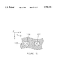
- FIG. 1 is a cross section side view of a flat, electrically nonconductive, substrate or plate member from which a printhead in accordance with the present invention is formed using electroforming techniques, this exemplary substrate having three cone-shaped ink jet nozzle holes preformed therein.
- FIG. 2 is a side view of the substrate of FIG. 1 after a first metal layer has been coated on all surfaces thereof, or at least on the ink entry side, the ink exit side, and the three nozzle cones thereof.
- FIG. 3 is side view of the substrate of FIG. 2 after the first metal layer shown in FIG. 2 has been selectively removed, by the use of photoresist and metal etching techniques, so as to leave three circles of the first metal layer that individually surround, and are continuous with, the three individual metal nozzle cones on the cone's ink entry side, so as to provide three electrical conductors (not shown in FIG. 3) of the first metal layer, each electrical conductor extending away from an individual metal circle for the purpose of facilitating the selective application of individual control voltages to the three metal nozzle cones, and so as to leave three circles of the first metal layer that individually surround, and are continuous with, the three individual metal nozzle cones on the cone's ink exit side.
- FIG. 4 is a top view of FIG. 3, this view showing the three electrical conductors that are formed on the cone's ink entry side.
- FIG. 5 is a side view of the substrate of FIGS. 3,4, wherein a second metal has been plated on each of the six metal circles, the three metal conductors, and the three metal nozzle cones of FIGS. 3,4.
- FIG. 6 is a side view of the substrate of FIG. 5, wherein the ink exit side of the substrate has been full surface lapped to thereby remove the three metal rings from the ink exit side of the three metal nozzle cones shown in FIG. 5.
- FIG. 7 is a side view of the substrate of FIG. 6, wherein the ink exit side of the substrate has been full surface etched to remove a depth of that side of the substrate, thus leaving a short, and generally circular, cylinder-shaped metal extension for each of the three cone-shaped metal nozzles, these three metal extensions extending beyond the now-etched ink exit side of the substrate by a common amount that is equal to amount of the substrate that was removed by the full surface etching thereof.
- FIG. 8 is a top or ink entry surface view of a substrate such as shown in FIG. 7, wherein the substrate contains a multi-nozzle array of nozzles arranged in an X-Y matrix array.
- FIG. 9 is a bottom or ink exit surface view of the multi-nozzle substrate of FIG. 8.
- FIG. 10 is a top or ink entry surface view of a signal multiplexing X-Y nozzle array in accordance with the invention.
- FIG. 11 is a bottom or ink exit surface view of the signal multiplexing X-Y nozzle array of FIG. 10.
- FIG. 12 is an enlarged side view of an edge portion of the multiplexing X-Y nozzle array of FIGS. 10 and 11.
- FIG. 13 is a side view of a printhead of the invention, whereby the nozzle substrate of FIG. 7, or the nozzle substrate of FIGS. 8 and 9, or the nozzle substrate of FIGS. 10, 11 and 12, is provided with a printing ink that is contained in a reservoir that is in communication with the ink entry side of the substrate.
- FIGS. 14-19 show a silicon embodiment of the invention, wherein FIG. 14 is a side view of a silicon semiconductor substrate having two square, cross-section nozzle holes etched therein, as shown in the section view of FIG. 15, wherein FIG. 16 shows two photoresist disks that have been deposited on the ink exit side of the silicon substrate, wherein FIG. 17 shows the silicon substrate after a depth of the silicon substrate has been removed from the ink exit side thereof, wherein FIG. 18 shows a finished silicon substrate having two metal nozzles, and wherein FIG. 19 is a top view, or ink entry surface view, of FIG. 18.
- the multi-nozzle ink jet printhead of the present invention preferably comprises a X-Y planar nozzle array that comprises a relatively large number of individually controllable nozzles.
- a number of generally parallel and multi-nozzle rows extend in the X direction that is shown by coordinate system 10 of FIG. 1.
- such a printhead is usually mounted at a stationary position, closely adjacent to a moving print medium (not shown) that moves in the Y direction.
- Ink filaments are selectively caused to move in the Z direction, these ink filaments traveling from selected printhead nozzles to thereafter deposit ink on selected pixels on the print substrate.
- selection of individual nozzles for emitting an ink filament may be made in accordance with a page map memory that electronically defines the printed content of a printed page.
- Equal increments of the Y direction of movement of the print substrate operate to define the X direction rows of pixels to be selectively printed on the print substrate, whereas the X direction physical spacing of the individual nozzles operate to define the Y direction columns of pixels that may be selectively printed on the print substrate; for example, one Y direction pixel column per nozzle. That is, the number of Y direction pixel columns per printed page is generally established by the physical spacing of the individual nozzles within the printhead, whereas the number of X direction pixel rows per printed page is generally established by controlling the printhead to emit ink in synchronism with the Y direction of movement of the print substrate.
- FIG. 1 is a cross-section side view of a flat, electrically nonconductive, substrate plate or member 11 from which a printhead in accordance with the invention is formed using electroforming techniques.
- substrate 10 is shown as having only three cone-shaped ink jet nozzles, or holes, 12,13,14 preformed therein, wherein nozzles 12,13,14 are aligned in the X direction, and wherein the central axis 20,21,22 of each individual cone-shaped nozzle 12,13,14 extends in the Z direction; i.e., central axes 20,21,22 are parallel.
- cone-shaped nozzle is intended to mean not only nozzles 12,13,14 having a conventional circular cross section when viewed in the X-Y plane of FIG. 1, that is a shape that is formed by rotating a right-triangle about a triangle leg that extends in the Z direction, but this term is also intended to include a cone-shaped nozzle having other X-Y planar cross-sectional shapes; for example, triangular, square or rectangular cross sectional shapes.
- the selected cone shape be truncated so as to provide a small cross sectional area 15 at the ink exit side 16 of the printhead and of substrate 11, and so as to provide a larger cross-sectional area 17 at the ink entry side 18 of the printhead and of substrate 11.
- the ink entry side 18 and the ink exit side 18 of substrate 11 lie in physically spaced and parallel X-Y planes.
- substrate 11 was formed of a structurally stable and electrically nonconductive engineering plastic, such as the brand Lexan polycarbonate, in which cone-shaped nozzles 12,13,14 were preformed as by molding, laser drilling or chemical etching.
- a structurally stable and electrically nonconductive engineering plastic such as the brand Lexan polycarbonate, in which cone-shaped nozzles 12,13,14 were preformed as by molding, laser drilling or chemical etching.
- the Z direction thickness 23 of substrate 11 was about 0.028-inch
- the diameter 24 of each large cone area 17 was about 0.015-inch
- the diameter 25 of each small cone area 15 was about 0.0065-inch
- the small cone areas 15 terminated in a circular cylinder portion having a Z direction dimension 26 of about 0.004-inch
- the large cone areas 17 terminated in a circular cylinder portion having a Z direction dimension 27 of about 0.005-inch.
- FIG. 2 is a side view of substrate 11, similar to FIG. 1, after a first metal layer 30 has been coated on all surfaces thereof, or at least on the ink entry side 18, the ink exit side 16, the internal surfaces of the three cones 12,13,14.
- First metal layer 30 comprises an electrically conductive seed-metal layer that is quite thin, for example about 3,000 angstroms thick.
- Metal layer 30 is preferably vacuum deposited (for example, by using sputtering or thermal evaporation processes, well known to those of skill in the art).
- layer 30 comprised chromium flash layer, followed by deposition of a copper layer.
- each individual cone-shaped metal nozzle when considered from the ink entry side 18 to the ink exit side 16, consists of a unitary metal surface having three portions; i.e., a circular cylinder 17, a conical surface 28, and a smaller circular cylinder 15.
- the upper end of circular cylinder 17, i.e., the end that is coincident with ink entry side 18, is continuous with the layer of first metal 30 that coats the full surface of ink entry side 18, whereas the lower end of circular cylinder 15, i.e., the end that is coincident with ink exit side 16, is continuous with the layer of first metal 30 that coats the full surface of ink exit side 16.
- FIG. 3 is a side view of substrate 11, similar to FIG. 2, and FIG. 4 is a top or ink entry view of substrate 11, after the first metal layer 30 that is shown in FIG. 2 has been selectively removed, by the use of well-known photoresist and metal etching techniques.
- substrate 11 of FIG. 2, full surface coated with metal 30, was full surface covered with a positive working photoresist, selected areas of the photoresist were exposed, the exposed areas of photoresist were removed as by etching, and the resulting uncovered areas of metal layer 30 were removed.
- This well-known photoresist/metal-etch process operates to leave three circles 31,32,33 of metal layer 30 on ink entry side 18, these three metal circles 31,32,33 individually surrounding and being continuous with the ink entry side of the three individual metal nozzle cones 12,13,14.
- ink entry side 18 also is now provided with three individual electrical conductors 34,35,36 of metal 30, as shown in the top view of FIG. 4. As shown in FIG. 4, each electrical conductor 34,35,36 extends away from an individual one of metal circles 31,32,33, these electrical conductors being provided for the purpose of facilitating the selective application of individual control voltages to the three metal nozzle cones 12,13,14.
- the edge-to-edge spacing 37 of adjacent metal circles 12,13,14 was about 0.012-inch, and the radial thickness 38 of each metal circle 12,13,14 was about 0.004-inch.
- the above-described photoresist/metal-etch process operated to leave a small metal ring 40,41,42 for each of the metal nozzle cones 12,13,14 on at the ink exit side 16 thereof.
- Metal rings 40,41,42 are provided for the purpose of ensuring adequate plating of a second metal layer, these rings will be removed by subsequent processing of substrate 11.
- FIG. 5 is a side view of substrate 11 of FIGS. 3,4, wherein a second metal 45 has been plated on each of the three metal circles 31,32,33, the three metal conductors 34,35,36, the three metal nozzle cones 12,13,14, and the three metal rings 40,41,42 of FIGS. 3,4.
- FIG. 5 also shows that after plating with this second metal 45, a metal stub 46,47,48 protrudes from the ink exit side 16 of the three metal nozzle cones 12,13,14.
- substrate 11 of FIGS. 3 and 4 was first immersed in a nickel-cobalt plating bath, and metal 30 was plated with a nickel-cobalt layer, to thereby form a first portion of the second metal. After rinsing, a thin layer of gold was preferably plated on the above-described nickel-cobalt layer, to thereby complete the second metal layer. Thereafter, the assembly of FIG. 5 was rinsed and dried. The use of a top gold layer is preferred for the purpose of inhibiting corrosion.
- FIG. 6 is a side view of substrate 11 of FIG. 5 after the ink exit side 16 thereof has been full surface lapped, to thereby remove metal protrusions 46,47,48 that are shown in FIG. 5.
- This lapping process operates primarily to remove metal protrusions 46,47,48, and may incidently remove a small portion of substrate 11 on the ink exit side 16 thereof.
- the ink exit side 16 of substrate 11, as shown in FIG. 6, first full surface lapped to remove metal portions 46,47,48 and thereafter substrate 11 is full surface etched to remove a uniform portion of that side of substrate 11.
- FIG. 7 is a side view of a completed substrate 11 after the ink exit side 16 of substrate 11, as seen in FIG. 6, has been full surface lapped, and then etched to remove a uniform substrate depth 50 from that side of substrate 11.
- dimension 50 is about 0.005-inch.
- each of the metal nozzle cones 12,13,14 is left with a relatively short, and generally circular-cylinder-shaped metal extension 51,52,53.
- the metal extensions 51,52,53 extend axial relative to metal nozzle cones 12,13,14, and generally correspond to metal circular cylinder portions 15 that were above-described relative to FIG. 2.
- Metal extensions 51,52,53 extend beyond the now-etched surface 54 of substrate 11 by an amount that is equal to the amount 50 of substrate 11 that was removed by the full surface etching of the substrate's exit side 16. Examples of well-known techniques that may be used to remove portion 50 of substrate 11 include plasma etching, E-beam etching, and Reactive Ion Etching (RIE).
- plasma etching E-beam etching
- RIE Reactive Ion Etching
- the exterior surfaces of metal extensions 51,52,53 i.e., the metal surfaces that are exposed by removal of the portion 50 of substrate 11, were then coated with a thin layer of gold.
- a substrate 11 in accordance with the present invention, and fabricated as described above, may contain a multi-nozzle X-Y array having a relatively large number of individual metal nozzles cones, each individual cone of which is of the type 12,13,14 above described.
- FIG. 8 is a top view, or ink entry surface 18 view, of such an X-Y nozzle array
- FIG. 9 is a bottom view, or ink exit surface 16 view, of the X-Y nozzle array of FIG. 8.
- one of the many individual nozzles within substrate 11 is identified by numeral 55.
- FIGS. 8 and 9 In this exemplary showing of a multi-nozzle substrate 11, eight X direction nozzle rows 60-67 are shown, these eight rows being identified by X direction lines 60-67 in FIGS. 8 and 9. While such a substrate 11 actually contains a relatively large number of Y direction nozzle columns, for purposes of simplicity, only a limited number of nozzle columns are shown in FIGS. 8 and 9, the physical position of these columns being provided by X direction staggering of the nozzles 55 that are within the eight nozzle rows 60-67.
- a multi-nozzle substrate 11 in accordance with the present invention can be constructed and arranged to facilitate selective control of the multiple nozzles, therein by using well-known control signal multiplexing techniques.
- substrate 11 again is fabricated, as described above, to contain a multi-nozzle X-Y nozzle array having a relatively large number of individual metal nozzles cones, each individual cone of which is of the type 12,13,14 above described.
- FIG. 10 is a top view, or ink entry surface 18 view, of such a signal multiplexing X-Y nozzle array.
- FIG. 11 is a bottom view, or ink exit surface 16 view, of the X-Y nozzle array of FIG. 10.
- one of the many individual nozzles that are within substrate 11 is identified by numeral 68.
- FIGS. 10 and 11 In this exemplary showing of a multi-nozzle substrate 11 that facilitates signal multiplexing to select any given nozzle or nozzles 68 for the printing of a page pixel or pixels, eight X direction nozzle rows 70-77 are shown, these eight rows being identified by X direction lines 70-77 in FIGS. 10 and 11. While substrate 11 of FIGS. 10 and 11 actually contains a relatively large number of Y direction nozzle columns, for purposes of simplicity, only a limited number of nozzle columns are shown in FIGS. 10 and 11, the physical position of these columns being provided by X direction staggering of the nozzles 68 that are within the eight nozzle rows 70-77.
- the X direction nozzle rows are signal-controlled by a number of row-selection electrical conductors that are all located on the ink entry side 18 of substrate 11, and that are all collectively identified by one reference numeral 78 in FIG. 10. As shown, each individual one of the conductors 78 electrically connects to four nozzles 68 that reside in four different ones of the X direction nozzle rows 70-77. As will be apparent to those of skill in the art, conductors 78 are fabricated, or manufactured, in accordance with the invention using the techniques that are above-described relative to FIGS. 3 and 4.
- the ink exit side 16 of substrate 11, as shown in FIG. 11, is fabricated, as above described, to contain seven column-selection metal electrical conductors 80-86 that physically extend in the X direction.
- multiplexing column-selection control signals are connected to conductors 80-86, in synchronism with connecting multiplexing row-selection control signals to conductors 78 of FIG. 10. More specifically, in order to select any nozzle 68 for printing, that nozzles conductor 78 must be activated, and the two conductors 80-86 that lie on opposite side of that nozzle must both be activated.
- the four conductors 80,82,84,86 are shown as each being provided with an individual electrical conductor signal 90,91,92,93 to which column-selection control signals are applied.
- the remaining conductors 81,83,85 are likewise provided with an individual column-selection conductor; for example, at the left hand side of FIG. 11, not shown therein.
- the ink exit side 16 of substrate 11, shown in FIG. 11, is preferably provided with a metal field compensation electrode 95, as is described in that copending patent application.
- electrode 95 is deposited on the ink exit side 16 of substrate 11 using the techniques that are above-described relative to FIGS. 2-6.
- FIG. 12 is an enlarged side view of a portion of the substrate 11 that is shown in FIGS. 10 and 11.
- one of the array-edge-located nozzles 68 that is within outer nozzle row 70 is shown in physical relation to both that nozzle's row-selection control conductor 78 and that nozzles's column-selection control conductor 80, as well as that nozzle's closely adjacent field compensation electrode 95.
- FIG. 13 is a side view of such an arrangement.
- substrate 11 is supported by, and physically sealed to, a Printed Circuit Board (PCB) 56, or to a similar structural member, that surrounds and structurally supports all four sides of substrate 11, leaving the center and nozzle-active portion of substrate 11 exposed both on its ink entry side 18, and on its ink exit side 16.
- PCB 56 operates to facilitate the connection of electrical control signals to the electrical conductors that are carried by the ink entry side 18 of substrate 11.
- Printing ink usually under ambient pressure, is supplied in a well-known manner to a reservoir 58 that is defined by housing 57, PCB 56, and substrate 11.
- multi-nozzle printhead substrate members as above described can also be made using well-known semiconductor processing techniques.
- FIGS. 14-18 provide a teaching of such a multi-nozzle substrate in accordance with the invention.
- FIG. 14 is a side view of a thin, flat, silicon semiconductor substrate 10 having a flat and X-Y planar ink entry side 101 that is parallel to flat and X-Y planar ink exit side 102.
- a photoresist layer 103 has been coated on ink entry surface 101 in such a manner to leave two circular voids 104,105 in photoresist layer 103.
- square cross-section nozzle holes 106,107 are then produced in substrate 101.
- the square cross-sectional shape of each of the nozzle holes 106,107 is shown in FIG. 15, FIG. 15 being a section view of nozzle hole 106 as shown in FIG. 14.
- FIG. 16 shows the silicon substrate 100 of FIG. 14 after photoresist layer 103 has been removed from ink entry side 101, and after two donut-shaped photoresist disks 108 and 109 have been placed on the ink exit side 103 of silicon substrate 100.
- each of the two photoresist disks 108,109 may include a square-shaped central opening 110,111 that is located to be axially coincident with the square ink exit shape of nozzle hole 106,107, respectively.
- FIG. 17 shows the silicon substrate 100 of FIG. 16 after well-known silicon etching techniques have been used to remove a depth 113 of silicon substrate 100, to thereby form a generally annular shaped silicon protrusion 114,115 at the ink exit ends of each of the respective nozzle holes 106,107.
- FIG. 18 shows a finished silicon substrate 100, wherein the photoresist disks 108,109 of FIG. 17 have been removed, and wherein two metal nozzles 116,117 have been plated on silicon substrate 100 at the respective locations of the two nozzles holes 106,107.
- each of the two metal nozzles 116,117 comprise a disk-shaped metal portion 120 that is coincident with the ink entry side 101 of substrate 100, a square cross section cone-shaped metal portion 121, and a disk-shaped metal portion 122 that is coincident with the ink exit side of each of the two silicon protrusions 114,115.
- the metal nozzles 116,117 may comprise nickel-cobalt upon which a thin layer of gold has been plated.
- substrate 100 of FIG. 18 is also intended for use as above described in relation to FIG. 13, and substrate 100 may, if desired, be constructed to facilitate multiplex control of a large number of metal nozzles, as above described.
- the various embodiments provide that the described metal ink jet nozzles will terminate at a nozzle-extension that extends a distance beyond the ink exit side of the substrate (for example, see metal extensions 51,52,53 and distance 50 of FIG. 7).
- This feature of the invention insures that the ink that resides in all of the various printhead nozzles will not undesirably wet the adjacent surface of the substrates ink exit side.
- this distance 50 is selected as a function of the small X-Y cross-sectional area of these nozzle terminations, and the physical properties of the ink that is used in the printhead. More specifically, when these nozzle extensions are of a circular cross section, this distance 50 is selected as a function of the diameter of the circular cross section, and more specifically, this distance 50 is selected to be generally equal to the diameter of the circular cross section.
Abstract
Description
Claims (30)
Priority Applications (2)
| Application Number | Priority Date | Filing Date | Title |
|---|---|---|---|
| US08/622,815 US5790151A (en) | 1996-03-27 | 1996-03-27 | Ink jet printhead and method of making |
| PCT/US1997/005090 WO1997035726A1 (en) | 1996-03-27 | 1997-03-25 | Ink jet printhead and method of making |
Applications Claiming Priority (1)
| Application Number | Priority Date | Filing Date | Title |
|---|---|---|---|
| US08/622,815 US5790151A (en) | 1996-03-27 | 1996-03-27 | Ink jet printhead and method of making |
Publications (1)
| Publication Number | Publication Date |
|---|---|
| US5790151A true US5790151A (en) | 1998-08-04 |
Family
ID=24495622
Family Applications (1)
| Application Number | Title | Priority Date | Filing Date |
|---|---|---|---|
| US08/622,815 Expired - Fee Related US5790151A (en) | 1996-03-27 | 1996-03-27 | Ink jet printhead and method of making |
Country Status (2)
| Country | Link |
|---|---|
| US (1) | US5790151A (en) |
| WO (1) | WO1997035726A1 (en) |
Cited By (80)
| Publication number | Priority date | Publication date | Assignee | Title |
|---|---|---|---|---|
| WO1999034981A1 (en) * | 1998-01-08 | 1999-07-15 | Lexmark International, Inc. | Nozzle array for printhead |
| WO1999065686A2 (en) * | 1998-06-19 | 1999-12-23 | Lexmark International, Inc. | A heater chip module and process for making same |
| US6137506A (en) * | 1994-06-13 | 2000-10-24 | Canon Kabushiki Kaisha | Ink jet recording head with a plurality of orifice plates |
| US6154234A (en) * | 1998-01-09 | 2000-11-28 | Hewlett-Packard Company | Monolithic ink jet nozzle formed from an oxide and nitride composition |
| US6196664B1 (en) * | 1997-01-30 | 2001-03-06 | Nec Corporation | Ink droplet eject apparatus and method |
| EP1121249A1 (en) * | 1998-10-16 | 2001-08-08 | Silverbrook Research Pty. Limited | Improvements relating to inkjet printers |
| EP1065059A3 (en) * | 1999-07-02 | 2001-10-04 | Canon Kabushiki Kaisha | Method for producing liquid discharge head, liquid discharge head, head cartridge, liquid discharging recording apparatus, method for producing silicon plate and silicon plate |
| US6371600B1 (en) * | 1998-06-15 | 2002-04-16 | Lexmark International, Inc. | Polymeric nozzle plate |
| US6420196B1 (en) * | 1998-10-16 | 2002-07-16 | Silverbrook Research Pty. Ltd | Method of forming an inkjet printhead using part of active circuitry layers to form sacrificial structures |
| US20020121274A1 (en) * | 1995-04-05 | 2002-09-05 | Aerogen, Inc. | Laminated electroformed aperture plate |
| US6467876B1 (en) * | 1997-09-10 | 2002-10-22 | Seiko Epson Corporation | Porous structure, ink-jet recording head, methods of their production, and ink jet recorder |
| US6604813B2 (en) | 2001-07-06 | 2003-08-12 | Illinois Tool Works Inc. | Low debris fluid jetting system |
| WO2004009284A1 (en) * | 2002-07-23 | 2004-01-29 | Matsushita Electric Industrial Co., Ltd. | Laser processing method and laser processing apparatus |
| US20040032440A1 (en) * | 1998-10-16 | 2004-02-19 | Silverbrook Research Pty Ltd | Temperature control in printheads having thermal actuators |
| US20040031150A1 (en) * | 1998-10-16 | 2004-02-19 | Kia Silverbrook | Manufacturing inkjet printheads with large numbers of nozzles |
| US20040079724A1 (en) * | 1998-09-09 | 2004-04-29 | Silverbrook Research Pty Ltd | Method of fabricating a fluid ejection device using a planarizing step |
| US20040092121A1 (en) * | 1998-10-16 | 2004-05-13 | Kia Silverbrook | Fabrication of a printhead chip incorporating a plurality of nozzle arrangements |
| US20040246308A1 (en) * | 1998-10-16 | 2004-12-09 | Silverbrook Research Pty Ltd | Thermal bend actuator with spatial thermal pattern |
| US20040246305A1 (en) * | 1998-10-16 | 2004-12-09 | Kia Silverbrook | Inkjet printhead having thermal bend actuator heating element electrically isolated from nozzle chamber ink |
| US20040263551A1 (en) * | 1998-10-16 | 2004-12-30 | Kia Silverbrook | Method and apparatus for firing ink from a plurality of nozzles on a printhead |
| US20050083377A1 (en) * | 1998-10-16 | 2005-04-21 | Kia Silverbrook | Printhead assembly incorporating an array of printhead chips on an ink distribution structure |
| US20050116990A1 (en) * | 1998-10-16 | 2005-06-02 | Kia Silverbrook | Inkjet printer using meniscus rim in nozzle chamber |
| US20050195245A1 (en) * | 2004-03-02 | 2005-09-08 | Kyouhei Yamada | Liquid droplet ejecting apparatus and method for producing same |
| US20050231560A1 (en) * | 1999-10-15 | 2005-10-20 | Silverbrook Research Pty Ltd | Micro-electromechanical liquid ejection device |
| US20050264607A1 (en) * | 1998-10-16 | 2005-12-01 | Silverbrook Research Pty Ltd | Printhead assembly with power and ground connections along single edge |
| US20050279090A1 (en) * | 1998-09-09 | 2005-12-22 | Silverbrook Research Pty Ltd | Micro-electromechanical integrated circuit device with laminated actuators |
| US20060119661A1 (en) * | 1999-10-19 | 2006-06-08 | Silverbrook Research Pty Ltd | Nozzle arrangement |
| US20060164489A1 (en) * | 2005-01-26 | 2006-07-27 | Ramon Vega | Latent inkjet printing, to avoid drying and liquid-loading problems, and provide sharper imaging |
| US20060174720A1 (en) * | 2002-01-24 | 2006-08-10 | Sensarray Corporation | Process condition sensing wafer and data analysis system |
| US20070081187A1 (en) * | 1998-11-09 | 2007-04-12 | Silverbrook Research Pty Ltd | Mobile telephone with printer and print media dispenser |
| US7237874B2 (en) | 2000-06-30 | 2007-07-03 | Silverbrook Research Pty Ltd | Inkjet printhead with grouped nozzles and a nozzle guard |
| US20070176968A1 (en) * | 1998-10-16 | 2007-08-02 | Silverbrook Research Pty Ltd | Pagewidth printhead having small print zone |
| US7360463B2 (en) | 2002-01-24 | 2008-04-22 | Sensarray Corporation | Process condition sensing wafer and data analysis system |
| US20080094432A1 (en) * | 1998-10-16 | 2008-04-24 | Silverbrook Research Pty Ltd | High nozzle density printhead ejecting low drop volumes |
| WO2009011709A1 (en) * | 2007-07-19 | 2009-01-22 | The Board Of Trustees Of The University Of Illinois | High resolution electrohydrodynamic jet printing for manufacturing systems |
| US20090145511A1 (en) * | 2006-01-10 | 2009-06-11 | Volker Till | Method of printing a pictorial image onto the circumferential outer surface of beverage bottles and filling beverage bottles in a bottling plant for filling bottles with a liquid beverage filling material in rotary filling machinery and apparatus therefor |
| US20090237433A1 (en) * | 1998-10-16 | 2009-09-24 | Silverbrook Research Pty Ltd | Printhead Integrated Circuit With Low Drive Transistor To Nozzle Area Ratio |
| US7677467B2 (en) | 2002-01-07 | 2010-03-16 | Novartis Pharma Ag | Methods and devices for aerosolizing medicament |
| US20100155098A1 (en) * | 2005-12-13 | 2010-06-24 | Kla-Tencor Corporation | Component package for maintaining safe operating temperature of components |
| US7748377B2 (en) | 2000-05-05 | 2010-07-06 | Novartis Ag | Methods and systems for operating an aerosol generator |
| US7771642B2 (en) | 2002-05-20 | 2010-08-10 | Novartis Ag | Methods of making an apparatus for providing aerosol for medical treatment |
| US20100289124A1 (en) * | 2004-06-04 | 2010-11-18 | The Board Of Trustees Of The University Of Illinois | Printable Semiconductor Structures and Related Methods of Making and Assembling |
| US7946291B2 (en) | 2004-04-20 | 2011-05-24 | Novartis Ag | Ventilation systems and methods employing aerosol generators |
| US7971588B2 (en) | 2000-05-05 | 2011-07-05 | Novartis Ag | Methods and systems for operating an aerosol generator |
| US20110170225A1 (en) * | 2010-01-08 | 2011-07-14 | John Rogers | High Resolution Printing of Charge |
| US7982296B2 (en) | 2004-06-04 | 2011-07-19 | The Board Of Trustees Of The University Of Illinois | Methods and devices for fabricating and assembling printable semiconductor elements |
| CN102267286A (en) * | 2011-06-14 | 2011-12-07 | 华中科技大学 | Array electric fluid power printing head |
| US8336545B2 (en) | 2000-05-05 | 2012-12-25 | Novartis Pharma Ag | Methods and systems for operating an aerosol generator |
| US8372726B2 (en) | 2008-10-07 | 2013-02-12 | Mc10, Inc. | Methods and applications of non-planar imaging arrays |
| US8389862B2 (en) | 2008-10-07 | 2013-03-05 | Mc10, Inc. | Extremely stretchable electronics |
| US8398001B2 (en) | 1999-09-09 | 2013-03-19 | Novartis Ag | Aperture plate and methods for its construction and use |
| US20130135392A1 (en) * | 2011-11-25 | 2013-05-30 | Samsung Electronics Co., Ltd. | Inkjet printing apparatus and method of forming nozzles |
| US20130235123A1 (en) * | 2012-03-06 | 2013-09-12 | Toshiba Tec Kabushiki Kaisha | Ink-jet head and manufacturing method of the same |
| US8536667B2 (en) | 2008-10-07 | 2013-09-17 | Mc10, Inc. | Systems, methods, and devices having stretchable integrated circuitry for sensing and delivering therapy |
| US8539944B2 (en) | 2002-01-07 | 2013-09-24 | Novartis Ag | Devices and methods for nebulizing fluids for inhalation |
| US8562095B2 (en) | 2010-11-01 | 2013-10-22 | The Board Of Trustees Of The University Of Illinois | High resolution sensing and control of electrohydrodynamic jet printing |
| US8561604B2 (en) | 1995-04-05 | 2013-10-22 | Novartis Ag | Liquid dispensing apparatus and methods |
| US8616195B2 (en) | 2003-07-18 | 2013-12-31 | Novartis Ag | Nebuliser for the production of aerosolized medication |
| US8666471B2 (en) | 2010-03-17 | 2014-03-04 | The Board Of Trustees Of The University Of Illinois | Implantable biomedical devices on bioresorbable substrates |
| US8681493B2 (en) | 2011-05-10 | 2014-03-25 | Kla-Tencor Corporation | Heat shield module for substrate-like metrology device |
| US8865489B2 (en) | 2009-05-12 | 2014-10-21 | The Board Of Trustees Of The University Of Illinois | Printed assemblies of ultrathin, microscale inorganic light emitting diodes for deformable and semitransparent displays |
| US8886334B2 (en) | 2008-10-07 | 2014-11-11 | Mc10, Inc. | Systems, methods, and devices using stretchable or flexible electronics for medical applications |
| US8934965B2 (en) | 2011-06-03 | 2015-01-13 | The Board Of Trustees Of The University Of Illinois | Conformable actively multiplexed high-density surface electrode array for brain interfacing |
| US9108211B2 (en) | 2005-05-25 | 2015-08-18 | Nektar Therapeutics | Vibration systems and methods |
| US20150283563A1 (en) * | 2005-06-06 | 2015-10-08 | Micron Technology, Inc. | Device for Controlling Placement of Nanoparticles |
| US9159635B2 (en) | 2011-05-27 | 2015-10-13 | Mc10, Inc. | Flexible electronic structure |
| US9171794B2 (en) | 2012-10-09 | 2015-10-27 | Mc10, Inc. | Embedding thin chips in polymer |
| US9289132B2 (en) | 2008-10-07 | 2016-03-22 | Mc10, Inc. | Catheter balloon having stretchable integrated circuitry and sensor array |
| JP2016155357A (en) * | 2015-02-26 | 2016-09-01 | ブラザー工業株式会社 | Liquid discharge device and method for manufacturing liquid discharge device |
| US9554484B2 (en) | 2012-03-30 | 2017-01-24 | The Board Of Trustees Of The University Of Illinois | Appendage mountable electronic devices conformable to surfaces |
| US9568167B2 (en) | 2006-06-02 | 2017-02-14 | Electro Scientific Industries, Inc. | Products with a patterned light-transmissive portion |
| US9691873B2 (en) | 2011-12-01 | 2017-06-27 | The Board Of Trustees Of The University Of Illinois | Transient devices designed to undergo programmable transformations |
| US9723122B2 (en) | 2009-10-01 | 2017-08-01 | Mc10, Inc. | Protective cases with integrated electronics |
| US9765934B2 (en) | 2011-05-16 | 2017-09-19 | The Board Of Trustees Of The University Of Illinois | Thermally managed LED arrays assembled by printing |
| US9936574B2 (en) | 2009-12-16 | 2018-04-03 | The Board Of Trustees Of The University Of Illinois | Waterproof stretchable optoelectronics |
| US10441185B2 (en) | 2009-12-16 | 2019-10-15 | The Board Of Trustees Of The University Of Illinois | Flexible and stretchable electronic systems for epidermal electronics |
| US10918298B2 (en) | 2009-12-16 | 2021-02-16 | The Board Of Trustees Of The University Of Illinois | High-speed, high-resolution electrophysiology in-vivo using conformal electronics |
| US10925543B2 (en) | 2015-11-11 | 2021-02-23 | The Board Of Trustees Of The University Of Illinois | Bioresorbable silicon electronics for transient implants |
| US11029198B2 (en) | 2015-06-01 | 2021-06-08 | The Board Of Trustees Of The University Of Illinois | Alternative approach for UV sensing |
| US11118965B2 (en) | 2015-06-01 | 2021-09-14 | The Board Of Trustees Of The University Of Illinois | Miniaturized electronic systems with wireless power and near-field communication capabilities |
Families Citing this family (3)
| Publication number | Priority date | Publication date | Assignee | Title |
|---|---|---|---|---|
| US10857815B2 (en) | 2016-07-19 | 2020-12-08 | Hewlett-Packard Development Company, L.P. | Printing systems |
| WO2018017063A1 (en) * | 2016-07-19 | 2018-01-25 | Hewlett-Packard Development Company, L.P. | Plasma treatment heads |
| US10532582B2 (en) | 2016-07-19 | 2020-01-14 | Hewlett-Packard Development Company, L.P. | Printing systems |
Citations (11)
| Publication number | Priority date | Publication date | Assignee | Title |
|---|---|---|---|---|
| US4169008A (en) * | 1977-06-13 | 1979-09-25 | International Business Machines Corporation | Process for producing uniform nozzle orifices in silicon wafers |
| US4528070A (en) * | 1983-02-04 | 1985-07-09 | Burlington Industries, Inc. | Orifice plate constructions |
| US4542386A (en) * | 1982-11-15 | 1985-09-17 | Dalemark Industries, Inc. | Ink jet printing system |
| US4716423A (en) * | 1985-11-22 | 1987-12-29 | Hewlett-Packard Company | Barrier layer and orifice plate for thermal ink jet print head assembly and method of manufacture |
| US4728392A (en) * | 1984-04-20 | 1988-03-01 | Matsushita Electric Industrial Co., Ltd. | Ink jet printer and method for fabricating a nozzle member |
| US4801995A (en) * | 1984-12-28 | 1989-01-31 | Kabushiki Kaisha Toshiba | Semiconductor device |
| US5006202A (en) * | 1990-06-04 | 1991-04-09 | Xerox Corporation | Fabricating method for silicon devices using a two step silicon etching process |
| US5041190A (en) * | 1990-05-16 | 1991-08-20 | Xerox Corporation | Method of fabricating channel plates and ink jet printheads containing channel plates |
| JPH04299150A (en) * | 1991-03-28 | 1992-10-22 | Seiko Epson Corp | Nozzle plate and manufacturing method therefor |
| WO1994027825A1 (en) * | 1993-05-20 | 1994-12-08 | Compaq Computer Corporation | Single side drive system interconnectable ink jet printhead and method of manufacturing the same |
| US5598195A (en) * | 1993-06-22 | 1997-01-28 | Fuji Xerox Co., Ltd. | Ink jet recording method |
-
1996
- 1996-03-27 US US08/622,815 patent/US5790151A/en not_active Expired - Fee Related
-
1997
- 1997-03-25 WO PCT/US1997/005090 patent/WO1997035726A1/en active Application Filing
Patent Citations (11)
| Publication number | Priority date | Publication date | Assignee | Title |
|---|---|---|---|---|
| US4169008A (en) * | 1977-06-13 | 1979-09-25 | International Business Machines Corporation | Process for producing uniform nozzle orifices in silicon wafers |
| US4542386A (en) * | 1982-11-15 | 1985-09-17 | Dalemark Industries, Inc. | Ink jet printing system |
| US4528070A (en) * | 1983-02-04 | 1985-07-09 | Burlington Industries, Inc. | Orifice plate constructions |
| US4728392A (en) * | 1984-04-20 | 1988-03-01 | Matsushita Electric Industrial Co., Ltd. | Ink jet printer and method for fabricating a nozzle member |
| US4801995A (en) * | 1984-12-28 | 1989-01-31 | Kabushiki Kaisha Toshiba | Semiconductor device |
| US4716423A (en) * | 1985-11-22 | 1987-12-29 | Hewlett-Packard Company | Barrier layer and orifice plate for thermal ink jet print head assembly and method of manufacture |
| US5041190A (en) * | 1990-05-16 | 1991-08-20 | Xerox Corporation | Method of fabricating channel plates and ink jet printheads containing channel plates |
| US5006202A (en) * | 1990-06-04 | 1991-04-09 | Xerox Corporation | Fabricating method for silicon devices using a two step silicon etching process |
| JPH04299150A (en) * | 1991-03-28 | 1992-10-22 | Seiko Epson Corp | Nozzle plate and manufacturing method therefor |
| WO1994027825A1 (en) * | 1993-05-20 | 1994-12-08 | Compaq Computer Corporation | Single side drive system interconnectable ink jet printhead and method of manufacturing the same |
| US5598195A (en) * | 1993-06-22 | 1997-01-28 | Fuji Xerox Co., Ltd. | Ink jet recording method |
Cited By (366)
| Publication number | Priority date | Publication date | Assignee | Title |
|---|---|---|---|---|
| US6137506A (en) * | 1994-06-13 | 2000-10-24 | Canon Kabushiki Kaisha | Ink jet recording head with a plurality of orifice plates |
| US8561604B2 (en) | 1995-04-05 | 2013-10-22 | Novartis Ag | Liquid dispensing apparatus and methods |
| US20020121274A1 (en) * | 1995-04-05 | 2002-09-05 | Aerogen, Inc. | Laminated electroformed aperture plate |
| US6196664B1 (en) * | 1997-01-30 | 2001-03-06 | Nec Corporation | Ink droplet eject apparatus and method |
| US7597435B2 (en) | 1997-07-15 | 2009-10-06 | Silverbrook Research Pty Ltd | Ink supply unit for an ink jet printer |
| US20080129809A1 (en) * | 1997-07-15 | 2008-06-05 | Silverbrook Research Pty Ltd | Ink Supply Unit For An Ink Jet Printer |
| US20030038854A1 (en) * | 1997-09-10 | 2003-02-27 | Seiko Epson Corporation | Porous structure, ink jet recording head, methods of their production, and ink jet recorder |
| US6467876B1 (en) * | 1997-09-10 | 2002-10-22 | Seiko Epson Corporation | Porous structure, ink-jet recording head, methods of their production, and ink jet recorder |
| US6821716B2 (en) * | 1997-09-10 | 2004-11-23 | Seiko Epson Corporation | Porous structure, ink jet recording head, methods of their production, and ink jet recorder |
| US6024440A (en) * | 1998-01-08 | 2000-02-15 | Lexmark International, Inc. | Nozzle array for printhead |
| WO1999034981A1 (en) * | 1998-01-08 | 1999-07-15 | Lexmark International, Inc. | Nozzle array for printhead |
| US6154234A (en) * | 1998-01-09 | 2000-11-28 | Hewlett-Packard Company | Monolithic ink jet nozzle formed from an oxide and nitride composition |
| US6371600B1 (en) * | 1998-06-15 | 2002-04-16 | Lexmark International, Inc. | Polymeric nozzle plate |
| US6164762A (en) * | 1998-06-19 | 2000-12-26 | Lexmark International, Inc. | Heater chip module and process for making same |
| WO1999065686A3 (en) * | 1998-06-19 | 2000-03-30 | Lexmark Int Inc | A heater chip module and process for making same |
| WO1999065686A2 (en) * | 1998-06-19 | 1999-12-23 | Lexmark International, Inc. | A heater chip module and process for making same |
| US20090244194A1 (en) * | 1998-09-09 | 2009-10-01 | Silverbrook Research Pty Ltd | Micro-Electromechanical Integrated Circuit Device With Laminated Actuators |
| US20070211112A1 (en) * | 1998-09-09 | 2007-09-13 | Silverbrook Research Pty Ltd | Ink jet printer nozzle assembly with micro-electromechanical paddles |
| US20050279090A1 (en) * | 1998-09-09 | 2005-12-22 | Silverbrook Research Pty Ltd | Micro-electromechanical integrated circuit device with laminated actuators |
| US20050189317A1 (en) * | 1998-09-09 | 2005-09-01 | Kia Silverbrook | Method of fabricating inkjet nozzle |
| US20040079724A1 (en) * | 1998-09-09 | 2004-04-29 | Silverbrook Research Pty Ltd | Method of fabricating a fluid ejection device using a planarizing step |
| US20050189316A1 (en) * | 1998-09-09 | 2005-09-01 | Kia Silverbrook | Method of fabricating micro-electromechanical inkjet nozzle |
| US20080309697A1 (en) * | 1998-10-16 | 2008-12-18 | Silverbrook Research Pty Ltd | Printhead of an inkjet printer having densely spaced nozzles |
| US7677686B2 (en) | 1998-10-16 | 2010-03-16 | Silverbrook Research Pty Ltd | High nozzle density printhead ejecting low drop volumes |
| US20040246305A1 (en) * | 1998-10-16 | 2004-12-09 | Kia Silverbrook | Inkjet printhead having thermal bend actuator heating element electrically isolated from nozzle chamber ink |
| US20040263551A1 (en) * | 1998-10-16 | 2004-12-30 | Kia Silverbrook | Method and apparatus for firing ink from a plurality of nozzles on a printhead |
| US20050030343A1 (en) * | 1998-10-16 | 2005-02-10 | Kia Silverbrook | Inkjet printhead chip with trace orientation to enhance performance characteristics |
| US20050037532A1 (en) * | 1998-10-16 | 2005-02-17 | Kia Silverbrook | Method of fabricating a micro-electromechanical actuator that includes drive circuitry |
| US20050036002A1 (en) * | 1998-10-16 | 2005-02-17 | Kia Silverbrook | Micro-electromechanical actuator that includes drive circuitry |
| US20050041063A1 (en) * | 1998-10-16 | 2005-02-24 | Kia Silverbrook | Pagewidth inkjet printhead incorporating an array of nozzle arrangements |
| US20050041052A1 (en) * | 1998-10-16 | 2005-02-24 | Kia Silverbrook | Method of operating an ink jet printhead within a predetermined temperature range |
| US20050052497A1 (en) * | 1998-10-16 | 2005-03-10 | Kia Silverbrook | Pagewidth Inkjet printhead assembly with actuator drive circuitry |
| US7524032B2 (en) | 1998-10-16 | 2009-04-28 | Silverbrook Research Pty Ltd | Inkjet nozzle assembly with resistive heating actuator |
| US20050093934A1 (en) * | 1998-10-16 | 2005-05-05 | Kia Silverbrook | Printer assembly and nozzle arrangement |
| US20050093933A1 (en) * | 1998-10-16 | 2005-05-05 | Kia Silverbrook | Thermal ink ejection actuator |
| US20050099466A1 (en) * | 1998-10-16 | 2005-05-12 | Kia Silverbrook | Printhead wafer with individual ink feed to each nozzle |
| US20050099465A1 (en) * | 1998-10-16 | 2005-05-12 | Kia Silverbrook | Printhead temperature feedback method for a microelectromechanical ink jet printhead |
| US20050097742A1 (en) * | 1998-10-16 | 2005-05-12 | Kia Silverbrook | Nozzle and drive circuitry fabrication method |
| US20050109730A1 (en) * | 1998-10-16 | 2005-05-26 | Kia Silverbrook | Printhead wafer etched from opposing sides |
| US20050110832A1 (en) * | 1998-10-16 | 2005-05-26 | Kia Silverbrook | Printhead and ink supply arrangement |
| US20050116990A1 (en) * | 1998-10-16 | 2005-06-02 | Kia Silverbrook | Inkjet printer using meniscus rim in nozzle chamber |
| US20050134649A1 (en) * | 1998-10-16 | 2005-06-23 | Kia Silverbrook | Printhead chip with nozzle arrangement for color printing |
| US20050140726A1 (en) * | 1998-10-16 | 2005-06-30 | Kia Silverbrook | Nozzle arrangement including an actuator |
| US6913347B2 (en) | 1998-10-16 | 2005-07-05 | Silverbrook Research Pty Ltd | Inkjet printhead chip with trace orientation to enhance performance characteristics |
| US20050146559A1 (en) * | 1998-10-16 | 2005-07-07 | Kia Silverbrook | Inkjet printhead chip with improved nozzle arrangement layout |
| US20050144781A1 (en) * | 1998-10-16 | 2005-07-07 | Kia Silverbrook | Fabricating an inkjet printhead with grouped nozzles |
| US20050146566A1 (en) * | 1998-10-16 | 2005-07-07 | Kia Silverbrook | Inkjet printhead that incorporates feed back sense lines |
| US20050144782A1 (en) * | 1998-10-16 | 2005-07-07 | Kia Silverbrook | Method of fabricating printhead IC using CTE matched wafer and sacrificial materials |
| US20050157042A1 (en) * | 1998-10-16 | 2005-07-21 | Kia Silverbrook | Printhead |
| US20050185021A1 (en) * | 1998-10-16 | 2005-08-25 | Silverbrook Research Pty Ltd | Ink jet printhead having columnar arrays of transistor drive circuits |
| US20040092121A1 (en) * | 1998-10-16 | 2004-05-13 | Kia Silverbrook | Fabrication of a printhead chip incorporating a plurality of nozzle arrangements |
| US20040031150A1 (en) * | 1998-10-16 | 2004-02-19 | Kia Silverbrook | Manufacturing inkjet printheads with large numbers of nozzles |
| US6938991B2 (en) | 1998-10-16 | 2005-09-06 | Silverbrook Research Pty Ltd | Thermal bend actuator with spatial thermal pattern |
| US6938994B2 (en) | 1998-10-16 | 2005-09-06 | Silverbrook Research Pty Ltd | Method of operating an ink jet printhead within a predetermined temperature range |
| EP1121249A1 (en) * | 1998-10-16 | 2001-08-08 | Silverbrook Research Pty. Limited | Improvements relating to inkjet printers |
| US20050225601A1 (en) * | 1998-10-16 | 2005-10-13 | Silverbrook Research Pty Ltd. | Inkjet printhead apparatus |
| US20050225602A1 (en) * | 1998-10-16 | 2005-10-13 | Silverbrook Research Pty Ltd | Printhead IC with actuator movement parallel to ink inlet flow |
| US20050225604A1 (en) * | 1998-10-16 | 2005-10-13 | Silverbrook Research Pty Ltd | Method of forming a nozzle rim |
| US8336990B2 (en) | 1998-10-16 | 2012-12-25 | Zamtec Limited | Ink supply unit for printhead of inkjet printer |
| US20050243134A1 (en) * | 1998-10-16 | 2005-11-03 | Silverbrook Research Pty Ltd | Printhead integrated circuit comprising thermal bend actuator |
| US20050248620A1 (en) * | 1998-10-16 | 2005-11-10 | Silverbrook Research Pty Ltd | Ink jet printhead assembly with an ink distribution manifold |
| US20050253897A1 (en) * | 1998-10-16 | 2005-11-17 | Silverbrook Research Pty Ltd | Inkjet printhead having grouped inkjet nozzles |
| US20050264607A1 (en) * | 1998-10-16 | 2005-12-01 | Silverbrook Research Pty Ltd | Printhead assembly with power and ground connections along single edge |
| US20050270335A1 (en) * | 1998-10-16 | 2005-12-08 | Silverbrook Research Pty Ltd | Method of fabricating a micro-electromechanical actuating mechanism |
| US20040032440A1 (en) * | 1998-10-16 | 2004-02-19 | Silverbrook Research Pty Ltd | Temperature control in printheads having thermal actuators |
| US6988789B2 (en) | 1998-10-16 | 2006-01-24 | Silverbrook Research Pty Ltd | Thermal ink ejection actuator |
| US6994424B2 (en) | 1998-10-16 | 2006-02-07 | Silverbrook Research Pty Ltd | Printhead assembly incorporating an array of printhead chips on an ink distribution structure |
| US6998278B2 (en) | 1998-10-16 | 2006-02-14 | Silverbrook Research Pty Ltd | Method of fabricating a micro-electromechanical actuator that includes drive circuitry |
| US7004563B2 (en) | 1998-10-16 | 2006-02-28 | Silverbrook Research Pty Ltd | Pagewidth inkjet printhead incorporating an array of nozzle arrangements |
| US7014785B2 (en) | 1998-10-16 | 2006-03-21 | Silverbrook Research Pty Ltd | Method of fabricating inkjet nozzle |
| US7032992B2 (en) | 1998-10-16 | 2006-04-25 | Silverbrook Research Pty Ltd | Inkjet printer using meniscus rim in nozzle chamber |
| US7032997B2 (en) | 1998-10-16 | 2006-04-25 | Silverbrook Research Pty Ltd | Micro-electromechanical actuator that includes drive circuitry |
| US20060092220A1 (en) * | 1998-10-16 | 2006-05-04 | Silverbrook Research Pty Ltd | Pagewidth inkjet printhead assembly with data and power supply mounted on ink distribution assembly |
| US20060098047A1 (en) * | 1998-10-16 | 2006-05-11 | Silverbrook Research Pty Ltd. | Pagewidth inkjet printhead assembly with longitudinally extending sets of nozzles |
| US7048868B2 (en) | 1998-10-16 | 2006-05-23 | Silverbrook Reseach Pty Ltd | Method of fabricating micro-electromechanical inkjet nozzle |
| US8087757B2 (en) | 1998-10-16 | 2012-01-03 | Silverbrook Research Pty Ltd | Energy control of a nozzle of an inkjet printhead |
| US7070258B2 (en) | 1998-10-16 | 2006-07-04 | Silverbrook Research Pty Ltd | Printhead and ink supply arrangement |
| US7073881B2 (en) | 1998-10-16 | 2006-07-11 | Silverbrook Research Pty Ltd | Temperature control in printheads having thermal actuators |
| US20060152551A1 (en) * | 1998-10-16 | 2006-07-13 | Silverbrook Research Pty Ltd | Printhead integrated circuit for a pagewidth inkjet printhead |
| US7080895B2 (en) | 1998-10-16 | 2006-07-25 | Silverbrook Research Pty Ltd | Inkjet printhead apparatus |
| US7080893B2 (en) | 1998-10-16 | 2006-07-25 | Silverbrook Research Pty Ltd | Ink jet printhead having columnar arrays of transistor drive circuits |
| US8066355B2 (en) | 1998-10-16 | 2011-11-29 | Silverbrook Research Pty Ltd | Compact nozzle assembly of an inkjet printhead |
| US7083262B2 (en) | 1998-10-16 | 2006-08-01 | Silverbrook Research Pty Ltd | Inkjet printhead chip with improved nozzle arrangement layout |
| US8061795B2 (en) | 1998-10-16 | 2011-11-22 | Silverbrook Research Pty Ltd | Nozzle assembly of an inkjet printhead |
| US7101020B2 (en) | 1998-10-16 | 2006-09-05 | Silverbrook Research Pty Ltd | Pagewidth inkjet printhead assembly with data and power supply mounted on ink distribution assembly |
| US7111924B2 (en) | 1998-10-16 | 2006-09-26 | Silverbrook Research Pty Ltd | Inkjet printhead having thermal bend actuator heating element electrically isolated from nozzle chamber ink |
| US20060227156A1 (en) * | 1998-10-16 | 2006-10-12 | Silverbrook Research Pty Ltd | Inkjet printhead having a pre-determined array of inkjet nozzle assemblies |
| US20060238571A1 (en) * | 1998-10-16 | 2006-10-26 | Silverbrook Research Pty Ltd | Printhead integrated circuit with coupled arrays of transistor drive circuits and nozzles |
| US7132056B2 (en) | 1998-10-16 | 2006-11-07 | Silverbrook Research Pty Ltd | Method of fabricating a fluid ejection device using a planarizing step |
| US20060250448A1 (en) * | 1998-10-16 | 2006-11-09 | Silverbrook Research Pty Ltd | Inkjet printhead having ink flow preventing actuators |
| US7134740B2 (en) | 1998-10-16 | 2006-11-14 | Silverbrook Research Pty Ltd | Pagewidth inkjet printhead assembly with actuator drive circuitry |
| US20060268048A1 (en) * | 1998-10-16 | 2006-11-30 | Silverbrook Research Pty Ltd | Inkjet printhead integrated circuit with optimized trace orientation |
| US20060268064A1 (en) * | 1998-10-16 | 2006-11-30 | Silverbrook Research Pty Ltd | Pagewidth printhead assembly with flexible tab film for supplying power and data to printhead integrated circuits |
| US7144519B2 (en) | 1998-10-16 | 2006-12-05 | Silverbrook Research Pty Ltd | Method of fabricating an inkjet printhead chip having laminated actuators |
| US20060274119A1 (en) * | 1998-10-16 | 2006-12-07 | Silverbrook Research Pty Ltd | Ink ejection nozzle with a thermal bend actuator |
| US20060274121A1 (en) * | 1998-10-16 | 2006-12-07 | Silverbrook Research Pty Ltd | Inkjet nozzle assembly with resistive heating actuator |
| US7147307B2 (en) | 1998-10-16 | 2006-12-12 | Silverbrook Research Pty Ltd | Printhead IC with actuator movement parallel to ink inlet flow |
| US7147304B2 (en) | 1998-10-16 | 2006-12-12 | Silverbrook Research Pty Ltd | Pagewidth inkjet printhead assembly with longitudinally extending sets of nozzles |
| US7152944B2 (en) | 1998-10-16 | 2006-12-26 | Silverbrook Research Pty Ltd | Ink jet printhead assembly with an ink distribution manifold |
| US7155823B2 (en) | 1998-10-16 | 2007-01-02 | Silverbrook Research Pty Ltd | Manufacturing inkjet printheads with large numbers of nozzles |
| US7159968B2 (en) | 1998-10-16 | 2007-01-09 | Silverbrook Research Pty Ltd | Printhead integrated circuit comprising thermal bend actuator |
| US20070008386A1 (en) * | 1998-10-16 | 2007-01-11 | Silverbrook Research Pty Ltd | Nozzle arrangement for an inkjet printhead having a thermal actuator and paddle |
| US7168167B2 (en) | 1998-10-16 | 2007-01-30 | Silverbrook Research Pty Ltd | Nozzle and drive circuitry fabrication method |
| US20070030315A1 (en) * | 1998-10-16 | 2007-02-08 | Silverbrook Research Pty Ltd. | Printhead with drive transistors and corresponding ink ejection actuators |
| US20070030321A1 (en) * | 1998-10-16 | 2007-02-08 | Silverbrook Research Pty Ltd | Ink supply unit for an ink jet printer |
| US7175775B2 (en) | 1998-10-16 | 2007-02-13 | Silverbrook Research Pty Ltd | Method of fabricating printhead IC using CTE matched wafer and sacrificial materials |
| US7178899B2 (en) | 1998-10-16 | 2007-02-20 | Silverbrook Research Pty Ltd | Printhead integrated circuit for a pagewidth inkjet printhead |
| US7182437B2 (en) | 1998-10-16 | 2007-02-27 | Silverbrook Research Pty Ltd | Inkjet printhead having ink flow preventing actuators |
| US8057014B2 (en) | 1998-10-16 | 2011-11-15 | Silverbrook Research Pty Ltd | Nozzle assembly for an inkjet printhead |
| US7188935B2 (en) | 1998-10-16 | 2007-03-13 | Silverbrook Research Pty Ltd | Printhead wafer with individual ink feed to each nozzle |
| US20070070133A1 (en) * | 1998-10-16 | 2007-03-29 | Silverbrook Research Pty Ltd | Ink supply unit for a printhead in an inkjet printer |
| US7198346B2 (en) | 1998-10-16 | 2007-04-03 | Silverbrook Research Pty Ltd | Inkjet printhead that incorporates feed back sense lines |
| US8047633B2 (en) | 1998-10-16 | 2011-11-01 | Silverbrook Research Pty Ltd | Control of a nozzle of an inkjet printhead |
| US20070081031A1 (en) * | 1998-10-16 | 2007-04-12 | Silverbrook Research Pty Ltd | Pagewidth printhead having sealed inkjet actuators |
| US7207656B2 (en) | 1998-10-16 | 2007-04-24 | Silverbrook Research Pty Ltd | Printhead configuration having acutely aligned nozzle actuators |
| US7210764B2 (en) | 1998-10-16 | 2007-05-01 | Silverbrook Research Pty Ltd | Printhead with drive transistors and corresponding ink ejection actuators |
| US7216956B2 (en) | 1998-10-16 | 2007-05-15 | Silverbrook Research Pty Ltd | Printhead assembly with power and ground connections along single edge |
| US20070109345A1 (en) * | 1998-10-16 | 2007-05-17 | Silverbrook Research Pty Ltd | Nozzle arrangement for an inkjet printhead with associated actuator drive ciircuitry |
| US7219427B2 (en) | 1998-10-16 | 2007-05-22 | Silverbrook Research Pty Ltd | Fabricating an inkjet printhead with grouped nozzles |
| US20070115316A1 (en) * | 1998-10-16 | 2007-05-24 | Silverbrook Research Pty Ltd | Inkjet printhead with a wafer assembly having an array of nozzle arrangments |
| US7226147B2 (en) | 1998-10-16 | 2007-06-05 | Silverbrook Research Pty Ltd | Printhead integrated circuit with coupled arrays of transistor drive circuits and nozzles |
| US7229154B2 (en) | 1998-10-16 | 2007-06-12 | Silverbrook Research Pty Ltd | Ink ejection nozzle with a thermal bend actuator |
| US20070146432A1 (en) * | 1998-10-16 | 2007-06-28 | Silverbrook Research Pty Ltd | Inkjet printhead with spillage pits |
| US8025355B2 (en) | 1998-10-16 | 2011-09-27 | Silverbrook Research Pty Ltd | Printer system for providing pre-heat signal to printhead |
| US20070176968A1 (en) * | 1998-10-16 | 2007-08-02 | Silverbrook Research Pty Ltd | Pagewidth printhead having small print zone |
| US20070176971A1 (en) * | 1998-10-16 | 2007-08-02 | Silverbrook Research Pty Ltd | Web printer with straight print media Path |
| US20070176967A1 (en) * | 1998-10-16 | 2007-08-02 | Silverbrook Research Pty Ltd | Photo printer for printing 6" x 4" photos |
| US20070182785A1 (en) * | 1998-10-16 | 2007-08-09 | Silverbrook Research Pty Ltd | Inkjet Printhead Incorporating Interleaved Actuator Tails |
| US20070182784A1 (en) * | 1998-10-16 | 2007-08-09 | Silverbrook Research Pty Ltd | Ink ejection nozzle arrangement with layered actuator mechanism |
| US20070188557A1 (en) * | 1998-10-16 | 2007-08-16 | Silverbrook Research Pty Ltd | Printer comprising small area print chips forming a pagewidth printhead |
| US20070188554A1 (en) * | 1998-10-16 | 2007-08-16 | Silverbrook Research Pty Ltd | Inkjet printhead with pairs of ink spread restriction pits |
| US20070188570A1 (en) * | 1998-10-16 | 2007-08-16 | Silverbrook Research Pty Ltd | Ink supply arrangement incorporating baffles in an ink distribution molding |
| US20070211102A1 (en) * | 1998-10-16 | 2007-09-13 | Silverbrook Research Pty Ltd | Ink Supply Arrangement Incorporating Sets of Passages for Carrying Respective Types of Ink |
| US8011757B2 (en) | 1998-10-16 | 2011-09-06 | Silverbrook Research Pty Ltd | Inkjet printhead with interleaved drive transistors |
| US20070222821A1 (en) * | 1998-10-16 | 2007-09-27 | Silverbrook Research Pty Ltd | Signaling method for printhead |
| US20070222819A1 (en) * | 1998-10-16 | 2007-09-27 | Silverbrook Research Pty Ltd | Printhead with small drive transistor to nozzle area ratio |
| US20070222807A1 (en) * | 1998-10-16 | 2007-09-27 | Silverbrook Research Pty Ltd | Printhead and method for contolling print quality using printhead temperature |
| US7284836B2 (en) | 1998-10-16 | 2007-10-23 | Silverbrook Research Pty Ltd | Nozzle arrangement including an actuator |
| US20080012923A1 (en) * | 1998-10-16 | 2008-01-17 | Silverbrook Research Pty Ltd | Printer incorporating a print roll unit supplying ink to a baffled ink supply unit |
| US7322680B2 (en) | 1998-10-16 | 2008-01-29 | Silverbrook Research Pty Ltd | Printer assembly and nozzle arrangement |
| US7331101B2 (en) | 1998-10-16 | 2008-02-19 | Silverbrook Research Pty Ltd | Method of fabricating a micro-electromechanical actuating mechanism |
| US7350906B2 (en) | 1998-10-16 | 2008-04-01 | Silverbrook Research Pty Ltd | Ink supply arrangement incorporating sets of passages for carrying respective types of ink |
| US7350901B2 (en) | 1998-10-16 | 2008-04-01 | Silverbrook Research Pty Ltd | Ink supply unit for an ink jet printer |
| US20080079760A1 (en) * | 1998-10-16 | 2008-04-03 | Silverbrook Research Pry Ltd | Printhead with variable nozzle firing sequence |
| US7976131B2 (en) | 1998-10-16 | 2011-07-12 | Silverbrook Research Pty Ltd | Printhead integrated circuit comprising resistive elements spaced apart from substrate |
| US20080094432A1 (en) * | 1998-10-16 | 2008-04-24 | Silverbrook Research Pty Ltd | High nozzle density printhead ejecting low drop volumes |
| US7370942B2 (en) | 1998-10-16 | 2008-05-13 | Silverbrook Research Pty Ltd | Ink supply arrangement incorporating baffles in an ink distribution molding |
| US7380339B2 (en) | 1998-10-16 | 2008-06-03 | Silverbrook Research Pty Ltd | Method of manufacturing a printhead wafer etched from opposing sides |
| US7380906B2 (en) | 1998-10-16 | 2008-06-03 | Silverbrook Research Pty Ltd | Printhead |
| US7380913B2 (en) | 1998-10-16 | 2008-06-03 | Silverbrook Research Pty Ltd | Ink jet printer nozzle assembly with micro-electromechanical paddles |
| US7971967B2 (en) | 1998-10-16 | 2011-07-05 | Silverbrook Research Pty Ltd | Nozzle arrangement with actuator slot protection barrier |
| US7384131B2 (en) | 1998-10-16 | 2008-06-10 | Silverbrook Research Pty Ltd | Pagewidth printhead having small print zone |
| US7387368B2 (en) | 1998-10-16 | 2008-06-17 | Silverbrook Reseach Pty Ltd | Pagewidth printhead having sealed inkjet actuators |
| US7396108B2 (en) | 1998-10-16 | 2008-07-08 | Silverbrook Research Pty Ltd | Pagewidth printhead assembly with flexible tab film for supplying power and data to printhead integrated circuits |
| US7401895B2 (en) | 1998-10-16 | 2008-07-22 | Silverbrook Research Pty Ltd | Inkjet printhead integrated circuit with optimized trace orientation |
| US20080192096A1 (en) * | 1998-10-16 | 2008-08-14 | Silverbrook Research Pty Ltd | Ink supply unit having a cover unit for positioning tape automated bonded film |
| US7416275B2 (en) | 1998-10-16 | 2008-08-26 | Silverbrook Research Pty Ltd | Printhead chip with nozzle arrangement for color printing |
| US20080204514A1 (en) * | 1998-10-16 | 2008-08-28 | Silverbrook Research Pty Ltd | Nozzle Arrangement Having An Actuator Slot Protection Barrier To Reduce Ink Wicking |
| US7419247B2 (en) | 1998-10-16 | 2008-09-02 | Silverbrook Research Pty Ltd | Printer comprising small area print chips forming a pagewidth printhead |
| US7419244B2 (en) | 1998-10-16 | 2008-09-02 | Silverbrook Research Pty Ltd | Ink ejection nozzle arrangement with layered actuator mechanism |
| US7971975B2 (en) | 1998-10-16 | 2011-07-05 | Silverbrook Research Pty Ltd | Inkjet printhead comprising actuator spaced apart from substrate |
| US20080211879A1 (en) * | 1998-10-16 | 2008-09-04 | Silverbrook Research Pty Ltd | Pagewidth inkjet printhead assembly with nozzle arrangements having actuator arms configured to be in thermal balance when in a quiescent state |
| US20080211877A1 (en) * | 1998-10-16 | 2008-09-04 | Silverbrook Research Pty Ltd | Inkjet Printhead Having Nozzle Arrangements With Ink Spreading Prevention Rims |
| US20080211876A1 (en) * | 1998-10-16 | 2008-09-04 | Silverbrook Research Pty Ltd | Printhead For Use In Camera Photo-Printing |
| US7971972B2 (en) | 1998-10-16 | 2011-07-05 | Silverbrook Research Pty Ltd | Nozzle arrangement with fully static CMOS control logic architecture |
| US20080246817A1 (en) * | 1998-10-16 | 2008-10-09 | Silverbrook Research Pty Ltd | Nozzle Arrangement With Control Logic Architecture For An Ink Jet Printhead |
| US7441867B2 (en) | 1998-10-16 | 2008-10-28 | Silverbrook Research Pty Ltd | Inkjet printhead having a pre-determined array of inkjet nozzle assemblies |
| US7442317B2 (en) | 1998-10-16 | 2008-10-28 | Silverbrook Research Pty Ltd | Method of forming a nozzle rim |
| US20080266361A1 (en) * | 1998-10-16 | 2008-10-30 | Silverbrook Research Pty Ltd | Energy control of a nozzle of an inkjet printhead |
| US20080266356A1 (en) * | 1998-10-16 | 2008-10-30 | Silverbrook Research Pty Ltd | Compact nozzle assembly of an inkjet printhead |
| US20080266341A1 (en) * | 1998-10-16 | 2008-10-30 | Silverbrook Research Pty Ltd | Control logic for an inkjet printhead |
| US20080273059A1 (en) * | 1998-10-16 | 2008-11-06 | Silverbrook Research Pty Ltd | Nozzle assembly of an inkjet printhead |
| US20080278559A1 (en) * | 1998-10-16 | 2008-11-13 | Silverbrook Research Pty Ltd | Printer assembly with a controller for maintaining a printhead at an equilibrium temperature |
| US20080303871A1 (en) * | 1998-10-16 | 2008-12-11 | Silverbrook Research Pty Ltd | Nozzle assembly for an inkjet printer for ejecting a low volume droplet |
| US20080303866A1 (en) * | 1998-10-16 | 2008-12-11 | Silverbrook Research Pty Ltd | Nozzle assembly for an inkjet printer for ejecting a low speed droplet |
| US20080309722A1 (en) * | 1998-10-16 | 2008-12-18 | Silverbrook Research Pty Ltd | Low pressure nozzle for an inkjet printer |
| US20080309696A1 (en) * | 1998-10-16 | 2008-12-18 | Silverbrook Research Pty Ltd | g of nozzles of a printhead of an inkjet printer |
| US20080309694A1 (en) * | 1998-10-16 | 2008-12-18 | Silverbrook Research Pty Ltd | Aperture of a nozzle assembly of an inkjet printer |
| US20080309695A1 (en) * | 1998-10-16 | 2008-12-18 | Silverbrook Research Pty Ltd | Nozzle assembly for an inkjet printer having a short drive transistor channel |
| US20080309693A1 (en) * | 1998-10-16 | 2008-12-18 | Silverbrook Research Pty Ltd | Nozzle assembly for ejecting small droplets |
| US20080309721A1 (en) * | 1998-10-16 | 2008-12-18 | Silverbrook Research Pty Ltd | Low voltage nozzle assembly for an inkjet printer |
| US20080309720A1 (en) * | 1998-10-16 | 2008-12-18 | Silverbrook Research Pty Ltd | Inkjet printer nozzle formed on a drive transistor and control logic |
| US7967422B2 (en) | 1998-10-16 | 2011-06-28 | Silverbrook Research Pty Ltd | Inkjet nozzle assembly having resistive element spaced apart from substrate |
| US20080309699A1 (en) * | 1998-10-16 | 2008-12-18 | Silverbrook Research Pty Ltd | Low energy consumption nozzle assembly for an inkjet printer |
| US20080316271A1 (en) * | 1998-10-16 | 2008-12-25 | Silverbrook Research Pty Ltd | Nozzle arrangement for an inkjet printer with ink wicking reduction |
| US20080316262A1 (en) * | 1998-10-16 | 2008-12-25 | Silverbrook Research Pty Ltd | Compact nozzle assembly for an inkjet printer |
| US20080316242A1 (en) * | 1998-10-16 | 2008-12-25 | Silverbrook Research Pty Ltd | Control Of A Nozzle Of An Inkjet Printhead |
| US20080316276A1 (en) * | 1998-10-16 | 2008-12-25 | Silverbrook Research Pty Ltd. | Printhead integrated circuit having an ink ejection member with a laminated structure |
| US20080316241A1 (en) * | 1998-10-16 | 2008-12-25 | Silverbrook Research Pty Ltd | Nozzle assembly for an inkjet printhead |
| US20090002470A1 (en) * | 1998-10-16 | 2009-01-01 | Silverbrook Research Pty Ltd | Camera Printhead Assembly With Baffles To Retard Ink Acceleration |
| US7950771B2 (en) | 1998-10-16 | 2011-05-31 | Silverbrook Research Pty Ltd | Printhead nozzle arrangement with dual mode thermal actuator |
| US7506966B2 (en) | 1998-10-16 | 2009-03-24 | Silverbrook Research Pty Ltd | Printer incorporating a print roll unit supplying ink to a baffled ink supply unit |
| US7517055B2 (en) | 1998-10-16 | 2009-04-14 | Silverbrook Research Pty Ltd | Nozzle arrangement for an inkjet printhead with associated actuator drive circuitry |
| US20050083377A1 (en) * | 1998-10-16 | 2005-04-21 | Kia Silverbrook | Printhead assembly incorporating an array of printhead chips on an ink distribution structure |
| US20040246308A1 (en) * | 1998-10-16 | 2004-12-09 | Silverbrook Research Pty Ltd | Thermal bend actuator with spatial thermal pattern |
| US7537314B2 (en) | 1998-10-16 | 2009-05-26 | Silverbrook Research Pty Ltd | Inkjet printhead having nozzle arrangements with ink spreading prevention rims |
| US7946671B2 (en) | 1998-10-16 | 2011-05-24 | Silverbrook Research Pty Ltd | Inkjet printer for photographs |
| US7549726B2 (en) | 1998-10-16 | 2009-06-23 | Silverbrook Research Pty Ltd | Inkjet printhead with a wafer assembly having an array of nozzle arrangements |
| US7556352B2 (en) | 1998-10-16 | 2009-07-07 | Silverbrook Research Pty Ltd | Inject printhead with outwarldy extending actuator tails |
| US7556353B2 (en) | 1998-10-16 | 2009-07-07 | Silverbrook Research Pty Ltd | Printhead with small drive transistor to nozzle area ratio |
| US7556351B2 (en) | 1998-10-16 | 2009-07-07 | Silverbrook Research Pty Ltd | Inkjet printhead with spillage pits |
| US7556361B2 (en) | 1998-10-16 | 2009-07-07 | Silverbrook Research Pty Ltd | Ink supply unit having a cover unit for positioning tape automated bonded film |
| US7556358B2 (en) | 1998-10-16 | 2009-07-07 | Silverbrook Research Pty Ltd | Micro-electromechanical integrated circuit device with laminated actuators |
| US7562963B2 (en) | 1998-10-16 | 2009-07-21 | Silverbrook Research Pty Ltd | Pagewidth inkjet printhead assembly with nozzle arrangements having actuator arms configured to be in thermal balance when in a quiescent state |
| US7562962B2 (en) | 1998-10-16 | 2009-07-21 | Silverbrook Research Pty Ltd | Printhead for use in camera photo-printing |
| US7938524B2 (en) | 1998-10-16 | 2011-05-10 | Silverbrook Research Pty Ltd | Ink supply unit for ink jet printer |
| US20090195614A1 (en) * | 1998-10-16 | 2009-08-06 | Silverbrook Research Pty Ltd | Inkjet Printhead Nozzle Arrangement With Actuator Arm Slot Protection Barrier |
| US20090195598A1 (en) * | 1998-10-16 | 2009-08-06 | Silverbrook Research Pty Ltd | Inkjet Printhead With Shared Ink Spread Restriction Walls |
| US20090201339A1 (en) * | 1998-10-16 | 2009-08-13 | Silverbrook Research Pty Ltd | Printhead Nozzle Having Shaped Heating Element |
| US7578569B2 (en) | 1998-10-16 | 2009-08-25 | Silverbrook Research Pty Ltd | Printhead with variable nozzle firing sequence |
| US20090213186A1 (en) * | 1998-10-16 | 2009-08-27 | Silvebrook Research Pty Ltd | Inkjet Printhead Having Plural Nozzle Arrangements Grouped In Pods |
| US7585047B2 (en) | 1998-10-16 | 2009-09-08 | Silverbrook Research Pty Ltd | Nozzle arrangement with control logic architecture for an ink jet printhead |
| US7591541B2 (en) | 1998-10-16 | 2009-09-22 | Silverbrook Research Pty Ltd | Nozzle arrangement having an actuator slot protection barrier to reduce ink wicking |
| US20090237461A1 (en) * | 1998-10-16 | 2009-09-24 | Silverbrook Research Pty Ltd | Ink ejection nozzle arrangement |
| US20090237450A1 (en) * | 1998-10-16 | 2009-09-24 | Silverbrook Research Pty Ltd | Inkjet Printhead and Printhead Nozzle Arrangement |
| US20090237433A1 (en) * | 1998-10-16 | 2009-09-24 | Silverbrook Research Pty Ltd | Printhead Integrated Circuit With Low Drive Transistor To Nozzle Area Ratio |
| US20090244193A1 (en) * | 1998-10-16 | 2009-10-01 | Silverbrook Research Pty Ltd | Inkjet printhead and printhead nozzle arrangement |
| US6420196B1 (en) * | 1998-10-16 | 2002-07-16 | Silverbrook Research Pty. Ltd | Method of forming an inkjet printhead using part of active circuitry layers to form sacrificial structures |
| EP1121249A4 (en) * | 1998-10-16 | 2002-07-03 | Silverbrook Res Pty Ltd | Improvements relating to inkjet printers |
| US20090256890A1 (en) * | 1998-10-16 | 2009-10-15 | Silverbrook Research Pty Ltd | Printhead Nozzle Arrangement With Dual Mode Thermal Actuator |
| US7611220B2 (en) | 1998-10-16 | 2009-11-03 | Silverbrook Research Pty Ltd | Printhead and method for controlling print quality using printhead temperature |
| US20090289979A1 (en) * | 1998-10-16 | 2009-11-26 | Silverbrook Research Pty Ltd | Inkjet Printhead With Drive Circuitry Controlling Variable Firing Sequences |
| US7625068B2 (en) | 1998-10-16 | 2009-12-01 | Silverbrook Research Pty Ltd | Spring of nozzles of a printhead of an inkjet printer |
| US7625067B2 (en) | 1998-10-16 | 2009-12-01 | Silverbrook Research Pty Ltd | Nozzle assembly for an inkjet printer having a short drive transistor channel |
| US7625061B2 (en) | 1998-10-16 | 2009-12-01 | Silverbrook Research Pty Ltd | Printhead integrated circuit having an ink ejection member with a laminated structure |
| US20090303290A1 (en) * | 1998-10-16 | 2009-12-10 | Silverbrook Research Pty Ltd | Nozzle Arrangement With Actuator Slot Protection Barrier |
| US20090303297A1 (en) * | 1998-10-16 | 2009-12-10 | Silverbrook Research Pty Ltd. | Ink Supply Unit For Ink Jet Printer |
| US7637582B2 (en) | 1998-10-16 | 2009-12-29 | Silverbrook Research Pty Ltd | Photo printer for printing 6″ × 4″ photos |
| US7654628B2 (en) | 1998-10-16 | 2010-02-02 | Silverbrook Research Pty Ltd | Signaling method for printhead |
| US7661797B2 (en) | 1998-10-16 | 2010-02-16 | Silverbrook Research Pty Ltd | Printhead of an inkjet printer having densely spaced nozzles |
| US7661796B2 (en) | 1998-10-16 | 2010-02-16 | Silverbrook Research Pty Ltd | Nozzle assembly for ejecting small droplets |
| US7669951B2 (en) | 1998-10-16 | 2010-03-02 | Silverbrook Research Pty Ltd | Low energy consumption nozzle assembly for an inkjet printer |
| US7669950B2 (en) | 1998-10-16 | 2010-03-02 | Silverbrook Research Pty Ltd | Energy control of a nozzle of an inkjet printhead |
| US7669964B2 (en) | 1998-10-16 | 2010-03-02 | Silverbrook Research Pty Ltd | Ink supply unit for a printhead in an inkjet printer |
| US20100053274A1 (en) * | 1998-10-16 | 2010-03-04 | Silverbrook Research Pty Ltd | Inkjet nozzle assembly having resistive element spaced apart from substrate |
| US20100053268A1 (en) * | 1998-10-16 | 2010-03-04 | Silverbrook Research Pty Ltd | Nozzle Arrangement With Laminated Ink Ejection Member And Ink Spread Prevention Rim |
| US20100053276A1 (en) * | 1998-10-16 | 2010-03-04 | Silverbrook Research Pty Ltd | Printhead Integrated Circuit Comprising Resistive Elements Spaced Apart From Substrate |
| US7934799B2 (en) | 1998-10-16 | 2011-05-03 | Silverbrook Research Pty Ltd | Inkjet printer with low drop volume printhead |
| US7524029B2 (en) | 1998-10-16 | 2009-04-28 | Silverbrook Research Pty Ltd | Inkjet printhead with pairs of ink spread restriction pits |
| US7931351B2 (en) | 1998-10-16 | 2011-04-26 | Silverbrook Research Pty Ltd | Inkjet printhead and printhead nozzle arrangement |
| US7677685B2 (en) | 1998-10-16 | 2010-03-16 | Silverbrook Research Pty Ltd | Nozzle assembly for an inkjet printer for ejecting a low volume droplet |
| US20100073441A1 (en) * | 1998-10-16 | 2010-03-25 | Silverbrook Research Pty Ltd | Ink Supply Unit For Printhead Of Inkjet Printer |
| US20100110130A1 (en) * | 1998-10-16 | 2010-05-06 | Silverbrook Research Pty Ltd | Printer System For Providing Pre-Heat Signal To Printhead |
| US20100110129A1 (en) * | 1998-10-16 | 2010-05-06 | Silvebrook Research Pty Ltd | Inkjet printer for photographs |
| US7735968B2 (en) | 1998-10-16 | 2010-06-15 | Silverbrook Research Pty Ltd | Inkjet printhead nozzle arrangement with actuator arm slot protection barrier |
| US20100149274A1 (en) * | 1998-10-16 | 2010-06-17 | Silverbrook Research Pty Ltd | Energy Control Of A Nozzle Of An Inkjet Printhead |
| US20100149268A1 (en) * | 1998-10-16 | 2010-06-17 | Silverbrook Research Pty Ltd | Inkjet Printer With Low Drop Volume Printhead |
| US7918540B2 (en) | 1998-10-16 | 2011-04-05 | Silverbrook Research Pty Ltd | Microelectromechanical ink jet printhead with printhead temperature feedback |
| US7918541B2 (en) | 1998-10-16 | 2011-04-05 | Silverbrook Research Pty Ltd | Micro-electromechanical integrated circuit device with laminated actuators |
| US7748827B2 (en) | 1998-10-16 | 2010-07-06 | Silverbrook Research Pty Ltd | Inkjet printhead incorporating interleaved actuator tails |
| US7753487B2 (en) | 1998-10-16 | 2010-07-13 | Silverbrook Research Pty Ltd | Aperture of a nozzle assembly of an inkjet printer |
| US7758162B2 (en) | 1998-10-16 | 2010-07-20 | Silverbrook Research Pty Ltd | Nozzle arrangement for an inkjet printer with ink wicking reduction |
| US7758160B2 (en) | 1998-10-16 | 2010-07-20 | Silverbrook Research Pty Ltd | Compact nozzle assembly for an inkjet printer |
| US7914115B2 (en) | 1998-10-16 | 2011-03-29 | Silverbrook Research Pty Ltd | Inkjet printhead and printhead nozzle arrangement |
| US7771025B2 (en) | 1998-10-16 | 2010-08-10 | Silverbrook Research Pty Ltd | Inkjet printhead having plural nozzle arrangements grouped in pods |
| US7905588B2 (en) | 1998-10-16 | 2011-03-15 | Silverbrook Research Pty Ltd | Camera printhead assembly with baffles to retard ink acceleration |
| US7771032B2 (en) | 1998-10-16 | 2010-08-10 | Silverbrook Research Pty Ltd | Printer assembly with a controller for maintaining a printhead at an equilibrium temperature |
| US7780264B2 (en) | 1998-10-16 | 2010-08-24 | Kia Silverbrook | Inkjet printer nozzle formed on a drive transistor and control logic |
| US7784905B2 (en) | 1998-10-16 | 2010-08-31 | Silverbrook Research Pty Ltd | Nozzle assembly for an inkjet printer for ejecting a low speed droplet |
| US7794050B2 (en) | 1998-10-16 | 2010-09-14 | Silverbrook Research Pty Ltd | Printhead nozzle having shaped heating element |
| US7815291B2 (en) | 1998-10-16 | 2010-10-19 | Silverbrook Research Pty Ltd | Printhead integrated circuit with low drive transistor to nozzle area ratio |
| US20100265298A1 (en) * | 1998-10-16 | 2010-10-21 | Silverbrook Research Pty Ltd | Inkjet printhead with interleaved drive transistors |
| US7901023B2 (en) | 1998-10-16 | 2011-03-08 | Silverbrook Research Pty Ltd | Inkjet printhead with drive circuitry controlling variable firing sequences |
| US20100277549A1 (en) * | 1998-10-16 | 2010-11-04 | Silverbrook Research Pty Ltd | Nozzle arrangement for inkjet printer with ink wicking reduction |
| US7896473B2 (en) | 1998-10-16 | 2011-03-01 | Silverbrook Research Pty Ltd | Low pressure nozzle for an inkjet printer |
| US20100295887A1 (en) * | 1998-10-16 | 2010-11-25 | Silverbrook Research Pty Ltd | Printer assembly with controller for maintaining printhead at equilibrium temperature |
| US7896468B2 (en) | 1998-10-16 | 2011-03-01 | Silverbrook Research Pty Ltd | Ink ejection nozzle arrangement |
| US7874644B2 (en) | 1998-10-16 | 2011-01-25 | Silverbrook Research Pty Ltd | Inkjet printhead with shared ink spread restriction walls |
| US7891773B2 (en) | 1998-10-16 | 2011-02-22 | Kia Silverbrook | Low voltage nozzle assembly for an inkjet printer |
| US7564580B2 (en) | 1998-11-09 | 2009-07-21 | Silverbrook Research Pty Ltd | Mobile telephone with printer and print media dispenser |
| US20070081187A1 (en) * | 1998-11-09 | 2007-04-12 | Silverbrook Research Pty Ltd | Mobile telephone with printer and print media dispenser |
| EP1065059A3 (en) * | 1999-07-02 | 2001-10-04 | Canon Kabushiki Kaisha | Method for producing liquid discharge head, liquid discharge head, head cartridge, liquid discharging recording apparatus, method for producing silicon plate and silicon plate |
| US8398001B2 (en) | 1999-09-09 | 2013-03-19 | Novartis Ag | Aperture plate and methods for its construction and use |
| US20050231560A1 (en) * | 1999-10-15 | 2005-10-20 | Silverbrook Research Pty Ltd | Micro-electromechanical liquid ejection device |
| US7419250B2 (en) | 1999-10-15 | 2008-09-02 | Silverbrook Research Pty Ltd | Micro-electromechanical liquid ejection device |
| US20060119661A1 (en) * | 1999-10-19 | 2006-06-08 | Silverbrook Research Pty Ltd | Nozzle arrangement |
| US7182431B2 (en) | 1999-10-19 | 2007-02-27 | Silverbrook Research Pty Ltd | Nozzle arrangement |
| US7748377B2 (en) | 2000-05-05 | 2010-07-06 | Novartis Ag | Methods and systems for operating an aerosol generator |
| US8336545B2 (en) | 2000-05-05 | 2012-12-25 | Novartis Pharma Ag | Methods and systems for operating an aerosol generator |
| US7971588B2 (en) | 2000-05-05 | 2011-07-05 | Novartis Ag | Methods and systems for operating an aerosol generator |
| US7237874B2 (en) | 2000-06-30 | 2007-07-03 | Silverbrook Research Pty Ltd | Inkjet printhead with grouped nozzles and a nozzle guard |
| US8196573B2 (en) | 2001-03-20 | 2012-06-12 | Novartis Ag | Methods and systems for operating an aerosol generator |
| US6604813B2 (en) | 2001-07-06 | 2003-08-12 | Illinois Tool Works Inc. | Low debris fluid jetting system |
| US7677467B2 (en) | 2002-01-07 | 2010-03-16 | Novartis Pharma Ag | Methods and devices for aerosolizing medicament |
| US8539944B2 (en) | 2002-01-07 | 2013-09-24 | Novartis Ag | Devices and methods for nebulizing fluids for inhalation |
| US20080228419A1 (en) * | 2002-01-24 | 2008-09-18 | Sensarray Corporation | Process condition sensing wafer and data analysis system |
| US7819033B2 (en) | 2002-01-24 | 2010-10-26 | Renken Wayne G | Process condition sensing wafer and data analysis system |
| US20100294051A1 (en) * | 2002-01-24 | 2010-11-25 | Kla-Tencor Corporation | Process condition sensing wafer and data analysis system |
| US7360463B2 (en) | 2002-01-24 | 2008-04-22 | Sensarray Corporation | Process condition sensing wafer and data analysis system |
| US9165846B2 (en) | 2002-01-24 | 2015-10-20 | Kla-Tencor Corporation | Process condition sensing wafer and data analysis system |
| US20060174720A1 (en) * | 2002-01-24 | 2006-08-10 | Sensarray Corporation | Process condition sensing wafer and data analysis system |
| US7757574B2 (en) | 2002-01-24 | 2010-07-20 | Kla-Tencor Corporation | Process condition sensing wafer and data analysis system |
| US20110040527A1 (en) * | 2002-01-24 | 2011-02-17 | Kla-Tencor Corporation | Process condition sensing wafer and data analysis system |
| US8033190B2 (en) | 2002-01-24 | 2011-10-11 | Kla-Tencor Technologies Corporation | Process condition sensing wafer and data analysis system |
| US7771642B2 (en) | 2002-05-20 | 2010-08-10 | Novartis Ag | Methods of making an apparatus for providing aerosol for medical treatment |
| WO2004009284A1 (en) * | 2002-07-23 | 2004-01-29 | Matsushita Electric Industrial Co., Ltd. | Laser processing method and laser processing apparatus |
| US8616195B2 (en) | 2003-07-18 | 2013-12-31 | Novartis Ag | Nebuliser for the production of aerosolized medication |
| US20050195245A1 (en) * | 2004-03-02 | 2005-09-08 | Kyouhei Yamada | Liquid droplet ejecting apparatus and method for producing same |
| US7946291B2 (en) | 2004-04-20 | 2011-05-24 | Novartis Ag | Ventilation systems and methods employing aerosol generators |
| US8664699B2 (en) | 2004-06-04 | 2014-03-04 | The Board Of Trustees Of The University Of Illinois | Methods and devices for fabricating and assembling printable semiconductor elements |
| US9768086B2 (en) | 2004-06-04 | 2017-09-19 | The Board Of Trustees Of The University Of Illinois | Methods and devices for fabricating and assembling printable semiconductor elements |
| US20100289124A1 (en) * | 2004-06-04 | 2010-11-18 | The Board Of Trustees Of The University Of Illinois | Printable Semiconductor Structures and Related Methods of Making and Assembling |
| US8039847B2 (en) | 2004-06-04 | 2011-10-18 | The Board Of Trustees Of The University Of Illinois | Printable semiconductor structures and related methods of making and assembling |
| US11088268B2 (en) | 2004-06-04 | 2021-08-10 | The Board Of Trustees Of The University Of Illinois | Methods and devices for fabricating and assembling printable semiconductor elements |
| US7982296B2 (en) | 2004-06-04 | 2011-07-19 | The Board Of Trustees Of The University Of Illinois | Methods and devices for fabricating and assembling printable semiconductor elements |
| US10374072B2 (en) | 2004-06-04 | 2019-08-06 | The Board Of Trustees Of The University Of Illinois | Methods and devices for fabricating and assembling printable semiconductor elements |
| US9450043B2 (en) | 2004-06-04 | 2016-09-20 | The Board Of Trustees Of The University Of Illinois | Methods and devices for fabricating and assembling printable semiconductor elements |
| US8394706B2 (en) | 2004-06-04 | 2013-03-12 | The Board Of Trustees Of The University Of Illinois | Printable semiconductor structures and related methods of making and assembling |
| US9761444B2 (en) | 2004-06-04 | 2017-09-12 | The Board Of Trustees Of The University Of Illinois | Methods and devices for fabricating and assembling printable semiconductor elements |
| US8440546B2 (en) | 2004-06-04 | 2013-05-14 | The Board Of Trustees Of The University Of Illinois | Methods and devices for fabricating and assembling printable semiconductor elements |
| US7677716B2 (en) | 2005-01-26 | 2010-03-16 | Hewlett-Packard Development Company, L.P. | Latent inkjet printing, to avoid drying and liquid-loading problems, and provide sharper imaging |
| US20060164489A1 (en) * | 2005-01-26 | 2006-07-27 | Ramon Vega | Latent inkjet printing, to avoid drying and liquid-loading problems, and provide sharper imaging |
| US9108211B2 (en) | 2005-05-25 | 2015-08-18 | Nektar Therapeutics | Vibration systems and methods |
| US20150283563A1 (en) * | 2005-06-06 | 2015-10-08 | Micron Technology, Inc. | Device for Controlling Placement of Nanoparticles |
| US9610593B2 (en) * | 2005-06-06 | 2017-04-04 | Micron Technology, Inc. | Device for positioning nanoparticles |
| US20100155098A1 (en) * | 2005-12-13 | 2010-06-24 | Kla-Tencor Corporation | Component package for maintaining safe operating temperature of components |
| US8604361B2 (en) | 2005-12-13 | 2013-12-10 | Kla-Tencor Corporation | Component package for maintaining safe operating temperature of components |
| US20090145511A1 (en) * | 2006-01-10 | 2009-06-11 | Volker Till | Method of printing a pictorial image onto the circumferential outer surface of beverage bottles and filling beverage bottles in a bottling plant for filling bottles with a liquid beverage filling material in rotary filling machinery and apparatus therefor |
| US9221275B2 (en) * | 2006-01-10 | 2015-12-29 | Khs Gmbh | Method of printing a pictorial image onto the circumferential outer surface of beverage bottles and filling beverage bottles in a bottling plant for filling bottles with a liquid beverage filling material in rotary filling machinery and apparatus therefor |
| US9568167B2 (en) | 2006-06-02 | 2017-02-14 | Electro Scientific Industries, Inc. | Products with a patterned light-transmissive portion |
| US9061494B2 (en) | 2007-07-19 | 2015-06-23 | The Board Of Trustees Of The University Of Illinois | High resolution electrohydrodynamic jet printing for manufacturing systems |
| US20110187798A1 (en) * | 2007-07-19 | 2011-08-04 | Rogers John A | High Resolution Electrohydrodynamic Jet Printing for Manufacturing Systems |
| US9487002B2 (en) | 2007-07-19 | 2016-11-08 | The Board Of Trustees Of The University Of Illinois | High resolution electrohydrodynamic jet printing for manufacturing systems |
| WO2009011709A1 (en) * | 2007-07-19 | 2009-01-22 | The Board Of Trustees Of The University Of Illinois | High resolution electrohydrodynamic jet printing for manufacturing systems |
| US8536667B2 (en) | 2008-10-07 | 2013-09-17 | Mc10, Inc. | Systems, methods, and devices having stretchable integrated circuitry for sensing and delivering therapy |
| US9516758B2 (en) | 2008-10-07 | 2016-12-06 | Mc10, Inc. | Extremely stretchable electronics |
| US9012784B2 (en) | 2008-10-07 | 2015-04-21 | Mc10, Inc. | Extremely stretchable electronics |
| US8372726B2 (en) | 2008-10-07 | 2013-02-12 | Mc10, Inc. | Methods and applications of non-planar imaging arrays |
| US8886334B2 (en) | 2008-10-07 | 2014-11-11 | Mc10, Inc. | Systems, methods, and devices using stretchable or flexible electronics for medical applications |
| US9289132B2 (en) | 2008-10-07 | 2016-03-22 | Mc10, Inc. | Catheter balloon having stretchable integrated circuitry and sensor array |
| US8389862B2 (en) | 2008-10-07 | 2013-03-05 | Mc10, Inc. | Extremely stretchable electronics |
| US10546841B2 (en) | 2009-05-12 | 2020-01-28 | The Board Of Trustees Of The University Of Illinois | Printed assemblies of ultrathin, microscale inorganic light emitting diodes for deformable and semitransparent displays |
| US8865489B2 (en) | 2009-05-12 | 2014-10-21 | The Board Of Trustees Of The University Of Illinois | Printed assemblies of ultrathin, microscale inorganic light emitting diodes for deformable and semitransparent displays |
| US9647171B2 (en) | 2009-05-12 | 2017-05-09 | The Board Of Trustees Of The University Of Illinois | Printed assemblies of ultrathin, microscale inorganic light emitting diodes for deformable and semitransparent displays |
| US9723122B2 (en) | 2009-10-01 | 2017-08-01 | Mc10, Inc. | Protective cases with integrated electronics |
| US9936574B2 (en) | 2009-12-16 | 2018-04-03 | The Board Of Trustees Of The University Of Illinois | Waterproof stretchable optoelectronics |
| US10441185B2 (en) | 2009-12-16 | 2019-10-15 | The Board Of Trustees Of The University Of Illinois | Flexible and stretchable electronic systems for epidermal electronics |
| US10918298B2 (en) | 2009-12-16 | 2021-02-16 | The Board Of Trustees Of The University Of Illinois | High-speed, high-resolution electrophysiology in-vivo using conformal electronics |
| US11057991B2 (en) | 2009-12-16 | 2021-07-06 | The Board Of Trustees Of The University Of Illinois | Waterproof stretchable optoelectronics |
| US9057994B2 (en) | 2010-01-08 | 2015-06-16 | The Board Of Trustees Of The University Of Illinois | High resolution printing of charge |
| US20110170225A1 (en) * | 2010-01-08 | 2011-07-14 | John Rogers | High Resolution Printing of Charge |
| US8666471B2 (en) | 2010-03-17 | 2014-03-04 | The Board Of Trustees Of The University Of Illinois | Implantable biomedical devices on bioresorbable substrates |
| US9986924B2 (en) | 2010-03-17 | 2018-06-05 | The Board Of Trustees Of The University Of Illinois | Implantable biomedical devices on bioresorbable substrates |
| US9278522B2 (en) | 2010-11-01 | 2016-03-08 | The Board Of Trustees Of The University Of Illinois | High resolution sensing and control of electrohydrodynamic jet printing |
| US8562095B2 (en) | 2010-11-01 | 2013-10-22 | The Board Of Trustees Of The University Of Illinois | High resolution sensing and control of electrohydrodynamic jet printing |
| US8681493B2 (en) | 2011-05-10 | 2014-03-25 | Kla-Tencor Corporation | Heat shield module for substrate-like metrology device |
| US9765934B2 (en) | 2011-05-16 | 2017-09-19 | The Board Of Trustees Of The University Of Illinois | Thermally managed LED arrays assembled by printing |
| US9159635B2 (en) | 2011-05-27 | 2015-10-13 | Mc10, Inc. | Flexible electronic structure |
| US8934965B2 (en) | 2011-06-03 | 2015-01-13 | The Board Of Trustees Of The University Of Illinois | Conformable actively multiplexed high-density surface electrode array for brain interfacing |
| US10349860B2 (en) | 2011-06-03 | 2019-07-16 | The Board Of Trustees Of The University Of Illinois | Conformable actively multiplexed high-density surface electrode array for brain interfacing |
| CN102267286B (en) * | 2011-06-14 | 2014-03-05 | 华中科技大学 | Array electric fluid power printing head |
| CN102267286A (en) * | 2011-06-14 | 2011-12-07 | 华中科技大学 | Array electric fluid power printing head |
| US20130135392A1 (en) * | 2011-11-25 | 2013-05-30 | Samsung Electronics Co., Ltd. | Inkjet printing apparatus and method of forming nozzles |
| US8888244B2 (en) * | 2011-11-25 | 2014-11-18 | Samsung Electronics Co., Ltd. | Inkjet printing apparatus and method of forming nozzles |
| US9691873B2 (en) | 2011-12-01 | 2017-06-27 | The Board Of Trustees Of The University Of Illinois | Transient devices designed to undergo programmable transformations |
| US10396173B2 (en) | 2011-12-01 | 2019-08-27 | The Board Of Trustees Of The University Of Illinois | Transient devices designed to undergo programmable transformations |
| US20130235123A1 (en) * | 2012-03-06 | 2013-09-12 | Toshiba Tec Kabushiki Kaisha | Ink-jet head and manufacturing method of the same |
| US9050798B2 (en) * | 2012-03-06 | 2015-06-09 | Toshiba Tec Kabushiki Kaisha | Ink-jet head and manufacturing method of the same |
| US10052066B2 (en) | 2012-03-30 | 2018-08-21 | The Board Of Trustees Of The University Of Illinois | Appendage mountable electronic devices conformable to surfaces |
| US10357201B2 (en) | 2012-03-30 | 2019-07-23 | The Board Of Trustees Of The University Of Illinois | Appendage mountable electronic devices conformable to surfaces |
| US9554484B2 (en) | 2012-03-30 | 2017-01-24 | The Board Of Trustees Of The University Of Illinois | Appendage mountable electronic devices conformable to surfaces |
| US9171794B2 (en) | 2012-10-09 | 2015-10-27 | Mc10, Inc. | Embedding thin chips in polymer |
| JP2016155357A (en) * | 2015-02-26 | 2016-09-01 | ブラザー工業株式会社 | Liquid discharge device and method for manufacturing liquid discharge device |
| US11029198B2 (en) | 2015-06-01 | 2021-06-08 | The Board Of Trustees Of The University Of Illinois | Alternative approach for UV sensing |
| US11118965B2 (en) | 2015-06-01 | 2021-09-14 | The Board Of Trustees Of The University Of Illinois | Miniaturized electronic systems with wireless power and near-field communication capabilities |
| US10925543B2 (en) | 2015-11-11 | 2021-02-23 | The Board Of Trustees Of The University Of Illinois | Bioresorbable silicon electronics for transient implants |
Also Published As
| Publication number | Publication date |
|---|---|
| WO1997035726A1 (en) | 1997-10-02 |
Similar Documents
| Publication | Publication Date | Title |
|---|---|---|
| US5790151A (en) | Ink jet printhead and method of making | |
| WO1997035726A9 (en) | Ink jet printhead and method of making | |
| EP0485182B1 (en) | Thermal inkjet thin film printhead having a plastic orifice plate and method of manufacture | |
| US5194877A (en) | Process for manufacturing thermal ink jet printheads having metal substrates and printheads manufactured thereby | |
| EP0509669B1 (en) | Thermal inkjet printhead orifice plate and method of manufacture | |
| JP2716174B2 (en) | Inkjet print head | |
| US5877791A (en) | Heat generating type ink-jet print head | |
| US6254219B1 (en) | Inkjet printhead orifice plate having related orifices | |
| US4954225A (en) | Method for making nozzle plates | |
| US4014029A (en) | Staggered nozzle array | |
| US4789425A (en) | Thermal ink jet printhead fabricating process | |
| CN101242956B (en) | Method for droplet ejection | |
| CA2376182C (en) | Device for manufacturing microarrays | |
| JPS6058707B2 (en) | Planar electrode for inkjet printing device and method for manufacturing the same | |
| JPH0639717A (en) | Manufacture of electric insulating material plate | |
| US3975741A (en) | Charge electrode for ink jet | |
| US7437820B2 (en) | Method of manufacturing a charge plate and orifice plate for continuous ink jet printers | |
| EP0426854B1 (en) | Ink-jet printing head and method of making it | |
| CN100418773C (en) | Liquid ejection element and manufacturing method therefor | |
| US7595004B2 (en) | Ink jet printhead and relative manufacturing process | |
| CN100522622C (en) | Method for manufacturing mandrel for electroformation of an orifice plate and the mandrel | |
| RU1800273C (en) | Method of multicolored jet printing, jet printing head to embody the method, and method of making the head | |
| GB2035908A (en) | Electrostatic print head and method of fabrication | |
| EP3969285B1 (en) | Electrohydrodynamic print head with structured feed layer | |
| US6402296B1 (en) | High resolution inkjet printer |
Legal Events
| Date | Code | Title | Description |
|---|---|---|---|
| AS | Assignment |
Owner name: IMAGING TECHNOLOGY INTERNATIONAL CORPORATION, COLO Free format text: ASSIGNMENT OF ASSIGNORS INTEREST;ASSIGNOR:MILIS, ROSS N.;REEL/FRAME:008070/0722 Effective date: 19960715 |
|
| FEPP | Fee payment procedure |
Free format text: PAYER NUMBER DE-ASSIGNED (ORIGINAL EVENT CODE: RMPN); ENTITY STATUS OF PATENT OWNER: SMALL ENTITY Free format text: PAYOR NUMBER ASSIGNED (ORIGINAL EVENT CODE: ASPN); ENTITY STATUS OF PATENT OWNER: SMALL ENTITY |
|
| FPAY | Fee payment |
Year of fee payment: 4 |
|
| REMI | Maintenance fee reminder mailed | ||
| FPAY | Fee payment |
Year of fee payment: 8 |
|
| AS | Assignment |
Owner name: DURST PHOTOTECHNIK AG, ITALY Free format text: SECURITY AGREEMENT;ASSIGNOR:IMAGING TECHNOLOGY INTERNATIONAL CORPORATION;REEL/FRAME:022597/0839 Effective date: 20070920 |
|
| REMI | Maintenance fee reminder mailed | ||
| LAPS | Lapse for failure to pay maintenance fees | ||
| STCH | Information on status: patent discontinuation |
Free format text: PATENT EXPIRED DUE TO NONPAYMENT OF MAINTENANCE FEES UNDER 37 CFR 1.362 |
|
| FP | Lapsed due to failure to pay maintenance fee |
Effective date: 20100804 |