US5858869A - Method for fabricating intermetal dielectric insulation using anisotropic plasma oxides and low dielectric constant polymers - Google Patents
Method for fabricating intermetal dielectric insulation using anisotropic plasma oxides and low dielectric constant polymers Download PDFInfo
- Publication number
- US5858869A US5858869A US08/868,343 US86834397A US5858869A US 5858869 A US5858869 A US 5858869A US 86834397 A US86834397 A US 86834397A US 5858869 A US5858869 A US 5858869A
- Authority
- US
- United States
- Prior art keywords
- conductive layer
- oxide
- dielectric constant
- low dielectric
- deposited
- Prior art date
- Legal status (The legal status is an assumption and is not a legal conclusion. Google has not performed a legal analysis and makes no representation as to the accuracy of the status listed.)
- Expired - Lifetime
Links
Images


Classifications
-
- H—ELECTRICITY
- H01—ELECTRIC ELEMENTS
- H01L—SEMICONDUCTOR DEVICES NOT COVERED BY CLASS H10
- H01L21/00—Processes or apparatus adapted for the manufacture or treatment of semiconductor or solid state devices or of parts thereof
- H01L21/02—Manufacture or treatment of semiconductor devices or of parts thereof
- H01L21/02104—Forming layers
- H01L21/02107—Forming insulating materials on a substrate
- H01L21/02109—Forming insulating materials on a substrate characterised by the type of layer, e.g. type of material, porous/non-porous, pre-cursors, mixtures or laminates
- H01L21/02112—Forming insulating materials on a substrate characterised by the type of layer, e.g. type of material, porous/non-porous, pre-cursors, mixtures or laminates characterised by the material of the layer
- H01L21/02118—Forming insulating materials on a substrate characterised by the type of layer, e.g. type of material, porous/non-porous, pre-cursors, mixtures or laminates characterised by the material of the layer carbon based polymeric organic or inorganic material, e.g. polyimides, poly cyclobutene or PVC
-
- H—ELECTRICITY
- H01—ELECTRIC ELEMENTS
- H01L—SEMICONDUCTOR DEVICES NOT COVERED BY CLASS H10
- H01L21/00—Processes or apparatus adapted for the manufacture or treatment of semiconductor or solid state devices or of parts thereof
- H01L21/02—Manufacture or treatment of semiconductor devices or of parts thereof
- H01L21/02104—Forming layers
- H01L21/02107—Forming insulating materials on a substrate
- H01L21/02109—Forming insulating materials on a substrate characterised by the type of layer, e.g. type of material, porous/non-porous, pre-cursors, mixtures or laminates
- H01L21/02112—Forming insulating materials on a substrate characterised by the type of layer, e.g. type of material, porous/non-porous, pre-cursors, mixtures or laminates characterised by the material of the layer
- H01L21/02123—Forming insulating materials on a substrate characterised by the type of layer, e.g. type of material, porous/non-porous, pre-cursors, mixtures or laminates characterised by the material of the layer the material containing silicon
- H01L21/02126—Forming insulating materials on a substrate characterised by the type of layer, e.g. type of material, porous/non-porous, pre-cursors, mixtures or laminates characterised by the material of the layer the material containing silicon the material containing Si, O, and at least one of H, N, C, F, or other non-metal elements, e.g. SiOC, SiOC:H or SiONC
- H01L21/02131—Forming insulating materials on a substrate characterised by the type of layer, e.g. type of material, porous/non-porous, pre-cursors, mixtures or laminates characterised by the material of the layer the material containing silicon the material containing Si, O, and at least one of H, N, C, F, or other non-metal elements, e.g. SiOC, SiOC:H or SiONC the material being halogen doped silicon oxides, e.g. FSG
-
- H—ELECTRICITY
- H01—ELECTRIC ELEMENTS
- H01L—SEMICONDUCTOR DEVICES NOT COVERED BY CLASS H10
- H01L21/00—Processes or apparatus adapted for the manufacture or treatment of semiconductor or solid state devices or of parts thereof
- H01L21/02—Manufacture or treatment of semiconductor devices or of parts thereof
- H01L21/02104—Forming layers
- H01L21/02107—Forming insulating materials on a substrate
- H01L21/02109—Forming insulating materials on a substrate characterised by the type of layer, e.g. type of material, porous/non-porous, pre-cursors, mixtures or laminates
- H01L21/02112—Forming insulating materials on a substrate characterised by the type of layer, e.g. type of material, porous/non-porous, pre-cursors, mixtures or laminates characterised by the material of the layer
- H01L21/02123—Forming insulating materials on a substrate characterised by the type of layer, e.g. type of material, porous/non-porous, pre-cursors, mixtures or laminates characterised by the material of the layer the material containing silicon
- H01L21/02164—Forming insulating materials on a substrate characterised by the type of layer, e.g. type of material, porous/non-porous, pre-cursors, mixtures or laminates characterised by the material of the layer the material containing silicon the material being a silicon oxide, e.g. SiO2
-
- H—ELECTRICITY
- H01—ELECTRIC ELEMENTS
- H01L—SEMICONDUCTOR DEVICES NOT COVERED BY CLASS H10
- H01L21/00—Processes or apparatus adapted for the manufacture or treatment of semiconductor or solid state devices or of parts thereof
- H01L21/02—Manufacture or treatment of semiconductor devices or of parts thereof
- H01L21/02104—Forming layers
- H01L21/02107—Forming insulating materials on a substrate
- H01L21/02109—Forming insulating materials on a substrate characterised by the type of layer, e.g. type of material, porous/non-porous, pre-cursors, mixtures or laminates
- H01L21/022—Forming insulating materials on a substrate characterised by the type of layer, e.g. type of material, porous/non-porous, pre-cursors, mixtures or laminates the layer being a laminate, i.e. composed of sublayers, e.g. stacks of alternating high-k metal oxides
-
- H—ELECTRICITY
- H01—ELECTRIC ELEMENTS
- H01L—SEMICONDUCTOR DEVICES NOT COVERED BY CLASS H10
- H01L21/00—Processes or apparatus adapted for the manufacture or treatment of semiconductor or solid state devices or of parts thereof
- H01L21/02—Manufacture or treatment of semiconductor devices or of parts thereof
- H01L21/02104—Forming layers
- H01L21/02107—Forming insulating materials on a substrate
- H01L21/02225—Forming insulating materials on a substrate characterised by the process for the formation of the insulating layer
- H01L21/0226—Forming insulating materials on a substrate characterised by the process for the formation of the insulating layer formation by a deposition process
- H01L21/02263—Forming insulating materials on a substrate characterised by the process for the formation of the insulating layer formation by a deposition process deposition from the gas or vapour phase
- H01L21/02271—Forming insulating materials on a substrate characterised by the process for the formation of the insulating layer formation by a deposition process deposition from the gas or vapour phase deposition by decomposition or reaction of gaseous or vapour phase compounds, i.e. chemical vapour deposition
- H01L21/02274—Forming insulating materials on a substrate characterised by the process for the formation of the insulating layer formation by a deposition process deposition from the gas or vapour phase deposition by decomposition or reaction of gaseous or vapour phase compounds, i.e. chemical vapour deposition in the presence of a plasma [PECVD]
-
- H—ELECTRICITY
- H01—ELECTRIC ELEMENTS
- H01L—SEMICONDUCTOR DEVICES NOT COVERED BY CLASS H10
- H01L21/00—Processes or apparatus adapted for the manufacture or treatment of semiconductor or solid state devices or of parts thereof
- H01L21/02—Manufacture or treatment of semiconductor devices or of parts thereof
- H01L21/02104—Forming layers
- H01L21/02107—Forming insulating materials on a substrate
- H01L21/02225—Forming insulating materials on a substrate characterised by the process for the formation of the insulating layer
- H01L21/0226—Forming insulating materials on a substrate characterised by the process for the formation of the insulating layer formation by a deposition process
- H01L21/02282—Forming insulating materials on a substrate characterised by the process for the formation of the insulating layer formation by a deposition process liquid deposition, e.g. spin-coating, sol-gel techniques, spray coating
-
- H—ELECTRICITY
- H01—ELECTRIC ELEMENTS
- H01L—SEMICONDUCTOR DEVICES NOT COVERED BY CLASS H10
- H01L21/00—Processes or apparatus adapted for the manufacture or treatment of semiconductor or solid state devices or of parts thereof
- H01L21/02—Manufacture or treatment of semiconductor devices or of parts thereof
- H01L21/04—Manufacture or treatment of semiconductor devices or of parts thereof the devices having at least one potential-jump barrier or surface barrier, e.g. PN junction, depletion layer or carrier concentration layer
- H01L21/18—Manufacture or treatment of semiconductor devices or of parts thereof the devices having at least one potential-jump barrier or surface barrier, e.g. PN junction, depletion layer or carrier concentration layer the devices having semiconductor bodies comprising elements of Group IV of the Periodic System or AIIIBV compounds with or without impurities, e.g. doping materials
- H01L21/30—Treatment of semiconductor bodies using processes or apparatus not provided for in groups H01L21/20 - H01L21/26
- H01L21/31—Treatment of semiconductor bodies using processes or apparatus not provided for in groups H01L21/20 - H01L21/26 to form insulating layers thereon, e.g. for masking or by using photolithographic techniques; After treatment of these layers; Selection of materials for these layers
- H01L21/314—Inorganic layers
- H01L21/316—Inorganic layers composed of oxides or glassy oxides or oxide based glass
- H01L21/31604—Deposition from a gas or vapour
- H01L21/31608—Deposition of SiO2
- H01L21/31612—Deposition of SiO2 on a silicon body
-
- H—ELECTRICITY
- H01—ELECTRIC ELEMENTS
- H01L—SEMICONDUCTOR DEVICES NOT COVERED BY CLASS H10
- H01L21/00—Processes or apparatus adapted for the manufacture or treatment of semiconductor or solid state devices or of parts thereof
- H01L21/70—Manufacture or treatment of devices consisting of a plurality of solid state components formed in or on a common substrate or of parts thereof; Manufacture of integrated circuit devices or of parts thereof
- H01L21/71—Manufacture of specific parts of devices defined in group H01L21/70
- H01L21/768—Applying interconnections to be used for carrying current between separate components within a device comprising conductors and dielectrics
- H01L21/76801—Applying interconnections to be used for carrying current between separate components within a device comprising conductors and dielectrics characterised by the formation and the after-treatment of the dielectrics, e.g. smoothing
- H01L21/76829—Applying interconnections to be used for carrying current between separate components within a device comprising conductors and dielectrics characterised by the formation and the after-treatment of the dielectrics, e.g. smoothing characterised by the formation of thin functional dielectric layers, e.g. dielectric etch-stop, barrier, capping or liner layers
- H01L21/76834—Applying interconnections to be used for carrying current between separate components within a device comprising conductors and dielectrics characterised by the formation and the after-treatment of the dielectrics, e.g. smoothing characterised by the formation of thin functional dielectric layers, e.g. dielectric etch-stop, barrier, capping or liner layers formation of thin insulating films on the sidewalls or on top of conductors
-
- H—ELECTRICITY
- H01—ELECTRIC ELEMENTS
- H01L—SEMICONDUCTOR DEVICES NOT COVERED BY CLASS H10
- H01L21/00—Processes or apparatus adapted for the manufacture or treatment of semiconductor or solid state devices or of parts thereof
- H01L21/70—Manufacture or treatment of devices consisting of a plurality of solid state components formed in or on a common substrate or of parts thereof; Manufacture of integrated circuit devices or of parts thereof
- H01L21/71—Manufacture of specific parts of devices defined in group H01L21/70
- H01L21/768—Applying interconnections to be used for carrying current between separate components within a device comprising conductors and dielectrics
- H01L21/76801—Applying interconnections to be used for carrying current between separate components within a device comprising conductors and dielectrics characterised by the formation and the after-treatment of the dielectrics, e.g. smoothing
- H01L21/76835—Combinations of two or more different dielectric layers having a low dielectric constant
-
- H—ELECTRICITY
- H01—ELECTRIC ELEMENTS
- H01L—SEMICONDUCTOR DEVICES NOT COVERED BY CLASS H10
- H01L23/00—Details of semiconductor or other solid state devices
- H01L23/52—Arrangements for conducting electric current within the device in operation from one component to another, i.e. interconnections, e.g. wires, lead frames
- H01L23/522—Arrangements for conducting electric current within the device in operation from one component to another, i.e. interconnections, e.g. wires, lead frames including external interconnections consisting of a multilayer structure of conductive and insulating layers inseparably formed on the semiconductor body
- H01L23/532—Arrangements for conducting electric current within the device in operation from one component to another, i.e. interconnections, e.g. wires, lead frames including external interconnections consisting of a multilayer structure of conductive and insulating layers inseparably formed on the semiconductor body characterised by the materials
- H01L23/5329—Insulating materials
-
- H—ELECTRICITY
- H01—ELECTRIC ELEMENTS
- H01L—SEMICONDUCTOR DEVICES NOT COVERED BY CLASS H10
- H01L2924/00—Indexing scheme for arrangements or methods for connecting or disconnecting semiconductor or solid-state bodies as covered by H01L24/00
- H01L2924/0001—Technical content checked by a classifier
- H01L2924/0002—Not covered by any one of groups H01L24/00, H01L24/00 and H01L2224/00
Definitions
- the present invention relates to a method for making integrated circuits on semiconductor substrates, and more particularly to a method for forming multilevel wiring on substrates with insulators having a low dielectric constant that reduce the RC time delays.
- the method is particularly useful for interconnections on ULSI circuits with minimum feature sizes less than 0.5 micrometers (um).
- Integrated circuits fabricated on semiconductor substrates for Ultra Large Scale Integration require multilevels of metal interconnections for electrically interconnecting the discrete semiconductor devices on the semiconductor chips.
- the different levels of interconnections are separated by layers of insulating material. These interposed insulating layers have etched via holes which are used to connect one level of metal to the next.
- the insulating layer is a silicon oxide (SiO 2 ) having a dielectric constant (relative to vacuum) of about 4.1 to 4.5.
- SiO 2 silicon oxide
- dielectric constant relative to vacuum
- the curve 1 shows the time delay in nanoseconds of the FET gate minimum feature size (channel length) in um (gate delay) and the curve 2 shows the interconnect delay as a function of the minimum feature size (line spacings).
- the interconnection delay (curve 2) becomes the predominant circuit delay. For example, below 0.5 um the gate delay (curve 1) decreases to about 0.1 E-9 seconds while the interconnect delay 2 increases rapidly to about 2.5 E-9 seconds.
- One approach to minimize these RC time delays is to use a good electrical conductor for the interconnections, such as replacing aluminium with copper to reduce resistance R, and in addition to use an insulating material that has a lower dielectric constant k, such as an organic, to reduce the capacitance C between lines.
- the improvement in the interconnect delay can best be understood by the family of curves in the prior art of FIG. 2 (Proceedings from the International Electronic Device Meeting (IEDM), 1995, page 244).
- RC 2pke o (4L 2 /P 2 +L 2 /T 2 ), where p is the metal resistivity, k is the relative dielectric constant, and e o is the permittivity in vacuum.
- the family of curves is shown for the interconnect RC time delay in nanoseconds (abscissa) as a function of metal thickness in micrometers (ordinate axis) for a metal line pitch of 0.8 um and having 10 mm lengths.
- the curve 2 shows the rapid increase in the interconnection delay (nsec.) as the metal thickness T is decreased for a constant pitch P and a metal length L of 0.8 um.
- the curve 3 is for aluminum (Al) lines having an intralevel dielectric constant k of 4, such as an undoped silicon oxide (SiO 2 ), while curve 4 shows the improvement in delay for comparable patterned copper lines using an insulator having the same dielectric constant k of 4.
- FIG. 3 is shown having closely spaced metal lines 16 formed on a substrate 10 having a silicon oxide layer 12.
- a conformal chemical vapor deposited liner 18, such as silicon oxide, is deposited by low temperature chemical vapor deposition (CVD) to protect the metal lines from the low k polymer that typically has high moisture content.
- the CVD lines also serve to improve the adhesion of the low k polymer 20 which is then deposited.
- a low dielectric polymer is deposited and planarized to provide an intermetal dielectric (IMD) layer.
- IMD intermetal dielectric
- a hard mask 22 composed of a low temperature CVD is deposited and a photoresist mask 24 is then patterned to form the via holes in the hard mask and in the low k polymer.
- a photoresist mask 24 is then patterned to form the via holes in the hard mask and in the low k polymer.
- problems associated with this structure One is the ability to control the chemical/mechanical polishing of the polymer to the top of the metal lines 16.
- Other problems are non-standard via hole etch, outgassing of moisture such as H 2 O in the via holes that can cause via poisoning, which can erode the next level of aluminum contacts, and low dielectric breakdown strength and high electrical leakage currents.
- the low k polymer also has the issue of a low mechanical strength and poor dimensional stability.
- thermal stability ⁇ 450° C.
- SOP spin-on polymer
- HSQ Hetachi Chemical polymer
- the oxides have a thermal conductivity K as measured in milliWatts/cm o C which is about 4 to 6 times better than the polymers.
- a CVD oxide is then deposited and contacts are etched to the metal lines without exposing the SOG.
- Chen et. al., in the Japanese Journal of Applied Physics, Vol 32 (1993) pp. 6119-6121, entitled “The Anisotropic Plasma-Enhanced Chemical Vapor Deposition SiO 2 /Spin-on Glass Process for 0.35 um Technology” teaches a method for forming an intermetal dielectric for sub-micrometer metal interconnections.
- a principal object of the present invention is to provide an anisotropic plasma oxide liner which enhances the gap-filling between the very closely spaced metal interconnections with a low dielectric constant (k) insulator, thereby providing low RC time delays for integrated circuits.
- a further object of this invention is to provide a stable fluorine-doped silicon oxide (FSG) having a low dielectric constant between the interlevel metallurgy to further reduce the RC time constant for the multilevel interconnections on integrated circuits and to provide better thermal cooling for the chip.
- FSG fluorine-doped silicon oxide
- a new method is achieved for forming multilevel interconnections with planar low dielectric constant insulators over a semiconductor substrate having partially completed semiconductor device structures, such as field effect transistors (FETs).
- An insulating layer is deposited over the semiconductor devices having contact openings to the devices.
- a barrier layer such as titanium (Ti)/titanium nitride (TiN) or titanium tungsten (TiW) is deposited to prevent penetration of the Al into the shallow junctions of the devices.
- a first conductive layer such as aluminum (Al), aluminum copper (AlCu), or Cu is deposited over the insulating layer and in the contact openings to regions of the semiconductor devices. The first conductive layer is patterned to form the interconnections for the devices.
- An anisotropic plasma oxide is deposited over the patterned first conductive layer.
- the anisotropic plasma oxide is deposited, which is thicker on the top surface than on the sidewalls of the conductive layer, having a ratio between the sidewall oxide thickness and top oxide thickness of about 0.17. This allows one to form more closely spaced conductive lines with a low dielectric constant insulator therebetween.
- a low dielectric constant insulator composed of an organic material, such as a polymer, is deposited on the anisotropic plasma oxide.
- the low dielectric constant insulator is chemical/mechanically polished essentially down to and into the anisotropic plasma oxide to the top surface of the patterned first conductive layer to form a planarized surface.
- a fluorine-doped oxide also having a relatively low dielectric constant of about 3.5, is deposited on the planar low dielectric insulator and on the exposed top surface of the patterned first conductive layer. Via holes are then etched in the fluorine-doped oxide to the first conductive layer to provide contacts for the second level of metal interconnections.
- a second conductive layer such as Al, Al/Cu, or Cu, is deposited on the fluorine-doped oxide and in the via holes, and is patterned to form the second level of metal interconnections. The process can be repeated to form additional levels of planar metal interconnections to complete the wiring of integrated circuits having these low RC time delays.
- FIG. 1 is a graph showing the dependence of the RC time delay for metal interconnections and gate electrode delay of an FET as a function of minimum feature size (um).
- FIG. 2 is a graph showing the rapid increase in the RC interconnection delays (nsec) as a function of metal thickness for thicknesses less than 0.5 um. Also shown is the dependence on the dielectric constant of the insulator and the electrical conductivity of the metals Al and Cu.
- FIG. 3 is a schematic cross-sectional view of a single level of metal interconnections depicting some of the current limitations of the prior art.
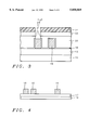
- FIGS. 4 through 9 are schematic cross-sectional views showing the sequence of process steps for planar metal interconnections, by the method of this invention, having the improved intermetal low dielectric material.
- FIG. 10 is a cross-sectional view of two adjacent metal lines that depicts the conventional use of PECVD oxide and low dielectric constant materials for making the intermetal dielectric layers.
- FIG. 11 is a cross-sectional view of two adjacent metal lines that depicts the improved intermetal dielectric layer using anisotropic plasma oxide and fluorinated oxide, by the method of this invention.
- FIG. 12 is a graph of the effective dielectric constant between metal lines as a function of the silicon oxide sidewall thickness on metal lines having a low dielectric material in the openings between the lines.
- FIG. 13 is a graph of the endpoint detect trace for the chemical/mechanical polishing back to planarize the low dielectric polymer and the anisotropic plasma oxide.
- the present invention relates to a method for fabricating low dielectric constant polymer intermetal dielectrics using anisotropic plasma oxide for metal interconnections on semiconductor substrates for ULSI circuits.
- the method utilizes an anisotropic plasma oxide to form a very thin oxide on the sidewalls of metal interconnection, which allows the line pitch to be significantly reduced thereby allowing the spacings to be filled with a low dielectric polymer.
- the thicker anisotropic plasma oxide on the top of the metal lines allows greater latitude in controlling the chem/mech polishing used to planarize the insulating layer.
- a fluoride-doped oxide between metal levels is used to further reduce the RC delay and to minimize via poisoning
- an insulating layer 12 is deposited on the semiconductor substrate 10 over the semiconductor devices to electrically insulate the devices from the first level of interconnections.
- Layer 12 is typically deposited by low pressure chemical vapor deposition (LPCVD) using a reactant gas such as tetraethosiloxane (TEOS), and is typically deposited to a thickness of between about 2000 and 20000 Angstroms.
- LPCVD low pressure chemical vapor deposition
- TEOS tetraethosiloxane
- a barrier layer such as titanium (Ti), titanium nitride (TiN), or titanium tungsten (TiW) is deposited to prevent penetration of Al into the shallow diffused junctions of the devices when the first level of interconnections is formed next.
- metal plugs such as tungsten, can be formed in the contact openings be provide electrical contacts to the devices.
- a first conductive layer 16 such as aluminum (Al), aluminum copper (AlCu), or copper (Cu) is deposited over the insulating layer 12 and in the contact openings (not shown) to regions of the semiconductor devices.
- the first conductive layer 16 is deposited by physical vapor deposition (PVD) or by sputter deposition to a thickness of between about 3000 and 10000 Angstroms.
- PVD physical vapor deposition
- sputter deposition to a thickness of between about 3000 and 10000 Angstroms.
- the first conductive layer 16 is then patterned by conventional photolithographic techniques and anisotropic plasma etching to form the interconnecting metal lines 16 for the devices.
- the anisotropic plasma etching can be carried out in a reactive ion etcher (RIE) using a reactant gas containing chlorine (Cl 2 ) and a carrier gas such as argon (Ar).
- RIE reactive ion etcher
- an intermetal dielectric (IMD) layer is formed by first depositing an anisotropic plasma oxide (APO) 18 over the metal lines 16.
- the anisotropic plasma oxide is deposited preferably by using a TEOS/O 2 chemistry resulting in a thicker oxide on the top surface of the metal lines 16 than on the sidewalls.
- the APO can have a ratio of oxide thicknesses on the sidewalls (18') of the metal lines to the oxide thickness on the top of the metal lines of about 0.1 to 0.5, and more specifically a ratio of 0.17.
- the APO layer 18 can be deposited, for example, from the reaction of TEOS with a helium/oxygen mixture in a parallel-plate RF plasma reactor.
- the APO layer is achieved by using a low oxygen flow rate, for example, the ratio of O 2 to TEOS flow rate can range between about 0 and 0.3.
- the APO can be deposited to a thickness of between about 1000 and 5000 Angstroms on the top of the metal lines, resulting in a sidewall coverage of between about 200 and 900 Angstroms, respectively. This provides a larger opening between the metal lines 16 for filling with a low dielectric constant insulator, such as a polymer, to reduce RC time delays.
- a low dielectric constant (k) insulator 20 composed of an organic material, such as a polymer, is deposited over the anisotropic plasma oxide layer 18 to a thickness sufficient to fill the openings between the metal lines 16, and more specifically to a thickness of between about 2000 and 20000 Angstroms.
- the low k layer 20 can be one of the organic materials, such as a polyimide.
- other low k materials such as polysilsequioxane (Si polymer), benzocyclobutene (BCB), fluorinated polyimide, and the like can be used to fill the openings.
- the low k polymer can be deposited, for example, by spin coating at a spin speed of between about 2000 and 4000 revolutions per minute (RPM), and is baked or annealed at a temperature of between about 80° and 450° C. for 0.5 to 2.0 minutes to cure the polymer.
- RPM revolutions per minute
- the low dielectric constant insulator 20 and the top portion of the anisotropic plasma oxide (APO) is polished back to the top surface of the metal lines 16 using chemical/mechanical polishing to provide a global planarized surface. Because of the thicker APO layer 18 on the top surface of the metal lines 16, it is easier to control the chemical/mechanical polishing (CMP) by providing a wider process window when the APO is polished back to the metal lines 16, as shown by the endpoint detect curves in FIG. 13.
- CMP chemical/mechanical polishing
- the endpoint graph shown in FIG. 13 shows the change in motor current (curve 200), and the change in pad temperature (curve 202) during polishing, either of which can be used to determine the endpoint for the polishing.
- Region E is the polish back in the low k insulator (20 in FIG. 7) and the polishing through the thicker anisotropic plasma oxide (18 in FIG. 7) on the top surface of the metal lines (16 in FIG. 7), which allows greater latitude in polishing time during removal of the APO in region D, while still providing a very thin APO (18' in FIG. 7) on the sidewalls of the metal lines.
- the abscissa (Y axis) on the left side of the graph shows the percent change in the motor current, while the abscissa on the right side of the graph shows the change in pad temperature in degrees Celsius.
- the ordinate (X axis) shows the polishing time in seconds.
- a fluorine-doped oxide (FSG) layer 22 is deposited over the planarized low dielectric insulator 20 and on the exposed top surface of the metal lines 16 formed from the patterned first conductive layer.
- layer 22 is deposited to a thickness of between about 2000 and 10000 Angstroms.
- the fluorine-doped oxide layer 22 is preferably formed by using plasma-enhanced chemical vapor deposition (PECVD), or a high-density plasma-enhanced CVD (HDPECVD), and a reactant gas such as TEOS to deposit a silicon oxide (SiO 2 ), and doping the SiO 2 with fluorine (F).
- the oxide is deposited at a temperature in the range of about 200° to 500° C.
- One method of doping the SiO 2 is by ion implanting F ions after the SiO 2 deposition, but preferably the method of doping the SiO 2 is by in-situ doping during the PECVD or HDPECVD using a reactant gas such as one of the following fluorine-containing gases: CF 4 , SiF 4 , C 2 F 6 , Si 2 F 4 , or SF 6 .
- the fluorine-doped oxide 22 is doped to a concentration of between about 2 and 8 atomic percent.
- the FSG is deposited in a reactor at a power of between about 400 and 600 Watts, at a pressure of between about 5 and 11 Torr using a gas mixture of about 600 sccm of TEOS, 900 sccm of O 2 , and 100 to 200 sccm of C 2 F 6 .
- the fluorine-doped oxide further reduces the RC delay time between the electrically conductive layers and minimizes via poisoning.
- the F-doped glass 22 has a much better thermal conductivity K than the low dielectric constant (k) polymers, and therefore is much more effective in removing the heat generated by the electric current (Joule heating) in the metal lines when the device is powered up.
- via holes 24 are etched in the FSG layer 22 to the metal lines 16 to provide contacts for the second level of metal interconnections.
- a second conductive layer 26, such as Al, Al/Cu, or Cu, is deposited on the fluorine-doped oxide 22 and in the via holes 24.
- Layer 26 is deposited similar to the deposition of the first conductive layer 16, for example, using physical vapor deposition, and to a thickness of between about 2000 and 20000 Angstroms.
- Layer 26 is patterned, for example, using reactive ion etching and a reactant gas mixture containing a chlorine (Cl 2 ) species and a carrier gas such as argon (Ar), to form the second level of metal interconnections.
- planar low k intermetal dielectric can be repeated to form additional levels of planar metal interconnections to complete the wiring of integrated circuits having these low RC time delays.
- FIG. 10 depicts a cross-sectional view of two adjacent metal lines 16 with a spacing S using the conventional PECVD layer 18 filled with a low k dielectric polymer 20.
- the dimensions T a show the thickness of the PECVD oxide over the metal
- T b shows the thickness of the PECVD oxide on the sidewalls of the metal lines.
- T c is the resulting gap formed between the adjacent metal lines, which is filled with the low k dielectric.
- FIG. 11 shows the corresponding adjacent metal lines 16 using the anisotropic PECVD oxide 18.
- the anisotropic PECVD oxide provides a much narrower sidewall oxide 18' having a width T b , which allows for a wider opening T c that the low k polymer can fill. This reduces the RC time delay.
- TABLES III and IV show a comparison of the resulting spacings T c filled with the low k constant for a series of top oxide thicknesses T a between 1000 and 5000 Angstroms.
- the first column, rows 1-5 is for the top oxide thickness (T a ) of the PECVD oxide in Angstroms. Col.
- TABLE IV for the anisotropic plasma oxide, the openings T c for the corresponding T a thickness of 2000 Angstroms and metal spacing S of 0.2 and 0.3 um, the openings T c are much wider having a width of 1320 and 2320 Angstroms, respectively. This allows one, by the method of this invention, to make more closely spaced lines having insulators with lower dielectric constants therebetween.
- the effective dielectric constant k for the insulator between metal lines is shown as a function of the linear oxide thickness T b for four different metal spacings.
- curve 102 is for 2000 Angstroms
- curve 103 is for 3000 Angstroms
- curve 104 is for 4000 Angstroms.
- the anisotropic plasma oxide (18 in FIG. 11) is deposited to a thickness of 2000 Angstroms
- the sidewall oxide T b (18' in FIG. 11) is only 340 Angstroms thick and provides a opening T c of 1320 Angstroms.
- FIG. 11 the anisotropic plasma oxide
- the vertical line 200 at 340 Angstroms thickness intersects the curve 102 represents an effective dielectric constant of only about 2.85 where the horizontal line 201 intersects the Y-axis.
Abstract
A method for making multilevel electrical interconnections having a planar intermetal dielectric (IMD) with low dielectric constant k and good thermal conductivity was achieved. The method involves patterning an electrically conductive layer to form metal lines on which is deposited an anisotropic plasma oxide (APO) resulting in a thin oxide on the sidewalls of the metal lines and a much thicker oxide on top of the lines. A low dielectric constant (k) polymer is deposited and the polymer and APO are chem/mech polished back to the top of the metal lines. A fluorine-doped silicon oxide (FSG) is deposited, and via holes are etched to provide electrical connections for the next level of interconnections. The APO provides wider openings between metal lines filled with the low k dielectric polymer thereby reducing the RC time delay of the circuit. The thick top APO provides more processing latitude for polishing back the APO and low k polymer. The FSG provides a lower dielectric constant k for further reducing the RC delay and a better thermal conductivity constant K for minimizing the Joule heating when the circuit is powered up. The process can be repeated several times to form a planar multilevel interconnection for completing wiring on the integrated circuit.
Description
(1) Field of the Invention
The present invention relates to a method for making integrated circuits on semiconductor substrates, and more particularly to a method for forming multilevel wiring on substrates with insulators having a low dielectric constant that reduce the RC time delays. The method is particularly useful for interconnections on ULSI circuits with minimum feature sizes less than 0.5 micrometers (um).
(2) Description of the Prior Art
Integrated circuits fabricated on semiconductor substrates for Ultra Large Scale Integration (ULSI) require multilevels of metal interconnections for electrically interconnecting the discrete semiconductor devices on the semiconductor chips. In the more conventional method the different levels of interconnections are separated by layers of insulating material. These interposed insulating layers have etched via holes which are used to connect one level of metal to the next. Typically, the insulating layer is a silicon oxide (SiO2) having a dielectric constant (relative to vacuum) of about 4.1 to 4.5. However, as the device dimensions decrease and the packing density increases, it is necessary to reduce the spacing between the metal lines in the interconnections to effectively wire up the integrated circuits. Unfortunately, as the spacing decreases, the intra- (on the same metal level) and interlevel (between metal levels) capacitances increase between metal lines when an insulating layer having the same dielectric constant is used since the capacitance C is inversely proportional to the spacing d between the lines (C=keA/d where k is the dielectric coefficient, e is the permittivity of the insulator, A is the area, and d is the spacing between lines). Therefore, it is very desirable to minimize the dielectric constant k in the insulator (dielectric) between the conducting lines to reduce the RC time constant and thereby increase the performance of the circuit (frequency response) since the signal propagation time in the circuit is adversely affected by the RC delay time, where R is the resistance of the metal line, and C is the inter- and/or the intralevel capacitance mentioned above. The dependence of delays due to the gate delays and the interconnects are shown in FIG. 1 reported at the International Symposium on VLSI, TSA, 1995, page 164. As shown in FIG. 1, the curve 1 shows the time delay in nanoseconds of the FET gate minimum feature size (channel length) in um (gate delay) and the curve 2 shows the interconnect delay as a function of the minimum feature size (line spacings). It is clearly seen that as the minimum feature size is reduced below 1.0 um, the interconnection delay (curve 2) becomes the predominant circuit delay. For example, below 0.5 um the gate delay (curve 1) decreases to about 0.1 E-9 seconds while the interconnect delay 2 increases rapidly to about 2.5 E-9 seconds.
One approach to minimize these RC time delays is to use a good electrical conductor for the interconnections, such as replacing aluminium with copper to reduce resistance R, and in addition to use an insulating material that has a lower dielectric constant k, such as an organic, to reduce the capacitance C between lines. The improvement in the interconnect delay can best be understood by the family of curves in the prior art of FIG. 2 (Proceedings from the International Electronic Device Meeting (IEDM), 1995, page 244). The RC expression for a metal line L with a pitch of P and a metal thickness T and an intermetal insulating layer also having a thickness T is given by RC=2pkeo (4L2 /P2 +L2 /T2), where p is the metal resistivity, k is the relative dielectric constant, and eo is the permittivity in vacuum. The family of curves is shown for the interconnect RC time delay in nanoseconds (abscissa) as a function of metal thickness in micrometers (ordinate axis) for a metal line pitch of 0.8 um and having 10 mm lengths. FIG. 2 shows the rapid increase in the interconnection delay (nsec.) as the metal thickness T is decreased for a constant pitch P and a metal length L of 0.8 um. The curve 3 is for aluminum (Al) lines having an intralevel dielectric constant k of 4, such as an undoped silicon oxide (SiO2), while curve 4 shows the improvement in delay for comparable patterned copper lines using an insulator having the same dielectric constant k of 4. Curves 5 and 6 show comparable improvement in the delay time for Al and Cu, respectively, using a low k interlevel dielectric of k=2, such as an organic polymer. For example, a number of inorganic and organic dielectrics are listed in TABLE I that can be used to reduce the RC delays.
              TABLE I
______________________________________
                  DIELECTRIC CONSTANT
______________________________________
INORGANICS
PLASMA SIO.sub.2    4.1-4.5
FLUORINE-DOPED SIO.sub.2
                    3.5
ORGANICS
POLYIMIDE           3.0-3.7
POLYSILSEQUIOXANE (Si POLYMER)
                    2.7-3.0
BENZOCYCLOBUTENE (BCB)
                    2.7
PARYLENE N          2.7
FLUORINATED POLYIMIDE
                    2.5
PARYLENE F          2.3
AMORPHOUS TEFLON    1.9
______________________________________
To better understand the problems associated with using a low dielectric polymer, FIG. 3 is shown having closely spaced metal lines 16 formed on a substrate 10 having a silicon oxide layer 12. A conformal chemical vapor deposited liner 18, such as silicon oxide, is deposited by low temperature chemical vapor deposition (CVD) to protect the metal lines from the low k polymer that typically has high moisture content. The CVD lines also serve to improve the adhesion of the low k polymer 20 which is then deposited. Typically a low dielectric polymer is deposited and planarized to provide an intermetal dielectric (IMD) layer. A hard mask 22 composed of a low temperature CVD is deposited and a photoresist mask 24 is then patterned to form the via holes in the hard mask and in the low k polymer. Typically there are several problems associated with this structure. One is the ability to control the chemical/mechanical polishing of the polymer to the top of the metal lines 16. Other problems are non-standard via hole etch, outgassing of moisture such as H2 O in the via holes that can cause via poisoning, which can erode the next level of aluminum contacts, and low dielectric breakdown strength and high electrical leakage currents. The low k polymer also has the issue of a low mechanical strength and poor dimensional stability. Another concern is poor thermal stability (<450° C.) that can be exacerbated by the Joule heating of the metal lines from high current density and poor thermal conductivity K of the polymers. For comparison the thermal conductivity of polymers such as polyimide, SOP (spin-on polymer), and HSQ (Hitachi Chemical polymer) are compared with the inorganic oxides plasma-enhanced PETEOS and high-density plasma (HDP) CVD in TABLE II.
              TABLE II
______________________________________
             Thermal Conductivity
                           Film Thickness
Dielectric Film
             K(mW/cm° C.)
                           (um)
______________________________________
PETEOS       11.5          0.1-3.8
HDP CVD Oxide
             12.0          1.0-1.8
Polyimide    2.4           3.3-9.0
SOP          2.4           0.34-0.5
HSQ          3.7           0.27-0.38
______________________________________
As can be seen the oxides have a thermal conductivity K as measured in milliWatts/cmo C which is about 4 to 6 times better than the polymers.
Several methods for forming planarized interconnections using low dielectric constant insulators have been described. For example, Jeng, U.S. Pat. No. 5,486,493, describes a method for forming closely spaced Al or titanium nitride/Al/titanium nitride interconnect lines having a low dielectric constant insulator between metal lines. Another method for making sub-micron metal interconnections using a spin-on glass (SOG) is described by Chen et al., U.S. Pat. No. 5,366,850, in which the SOG is cured and partially etched back to an insulating liner on the metal lines to form a planar surface. A CVD oxide is then deposited and contacts are etched to the metal lines without exposing the SOG. Chen et. al., in the Japanese Journal of Applied Physics, Vol 32 (1993) pp. 6119-6121, entitled "The Anisotropic Plasma-Enhanced Chemical Vapor Deposition SiO2 /Spin-on Glass Process for 0.35 um Technology" teaches a method for forming an intermetal dielectric for sub-micrometer metal interconnections.
As the spacings between interconnecting metal lines are further reduced, such as in future 0.18-0.13 micrometer technologies, it becomes increasingly difficult to provide an insulating layer having a low dielectric constant between adjacent metal lines and further to provide good thermal conductivity for cooling the circuit. There is also a need for providing a process with greater latitude for forming a planar low k dielectric layer, which is free of poisoned via holes (outgassing problems) that can degrade the metal contacts. Therefore there is still a strong need in the semiconductor industry for providing a simplified method for forming multilevel metal interconnections having reduced inter- and intralevel capacitance to reduce the RC time constant that improves circuit performance.
A principal object of the present invention is to provide an anisotropic plasma oxide liner which enhances the gap-filling between the very closely spaced metal interconnections with a low dielectric constant (k) insulator, thereby providing low RC time delays for integrated circuits.
It is another object of this invention to use an anisotropic plasma oxide which allows the low k polymers (insulators) to be chemical/mechanically polished back with greater processing latitude.
A further object of this invention is to provide a stable fluorine-doped silicon oxide (FSG) having a low dielectric constant between the interlevel metallurgy to further reduce the RC time constant for the multilevel interconnections on integrated circuits and to provide better thermal cooling for the chip.
In accordance with the objects of this invention, a new method is achieved for forming multilevel interconnections with planar low dielectric constant insulators over a semiconductor substrate having partially completed semiconductor device structures, such as field effect transistors (FETs). An insulating layer is deposited over the semiconductor devices having contact openings to the devices. A barrier layer such as titanium (Ti)/titanium nitride (TiN) or titanium tungsten (TiW) is deposited to prevent penetration of the Al into the shallow junctions of the devices. A first conductive layer, such as aluminum (Al), aluminum copper (AlCu), or Cu is deposited over the insulating layer and in the contact openings to regions of the semiconductor devices. The first conductive layer is patterned to form the interconnections for the devices. An anisotropic plasma oxide is deposited over the patterned first conductive layer. The anisotropic plasma oxide is deposited, which is thicker on the top surface than on the sidewalls of the conductive layer, having a ratio between the sidewall oxide thickness and top oxide thickness of about 0.17. This allows one to form more closely spaced conductive lines with a low dielectric constant insulator therebetween. A low dielectric constant insulator, composed of an organic material, such as a polymer, is deposited on the anisotropic plasma oxide. The low dielectric constant insulator is chemical/mechanically polished essentially down to and into the anisotropic plasma oxide to the top surface of the patterned first conductive layer to form a planarized surface. To further reduce the RC delay time between conductive layers and to minimize via poisoning, a fluorine-doped oxide, also having a relatively low dielectric constant of about 3.5, is deposited on the planar low dielectric insulator and on the exposed top surface of the patterned first conductive layer. Via holes are then etched in the fluorine-doped oxide to the first conductive layer to provide contacts for the second level of metal interconnections. A second conductive layer, such as Al, Al/Cu, or Cu, is deposited on the fluorine-doped oxide and in the via holes, and is patterned to form the second level of metal interconnections. The process can be repeated to form additional levels of planar metal interconnections to complete the wiring of integrated circuits having these low RC time delays.
The objectives and other advantages of this invention are best understood with reference to the preferred embodiment and drawings.
FIG. 1 is a graph showing the dependence of the RC time delay for metal interconnections and gate electrode delay of an FET as a function of minimum feature size (um).
FIG. 2 is a graph showing the rapid increase in the RC interconnection delays (nsec) as a function of metal thickness for thicknesses less than 0.5 um. Also shown is the dependence on the dielectric constant of the insulator and the electrical conductivity of the metals Al and Cu.
FIG. 3 is a schematic cross-sectional view of a single level of metal interconnections depicting some of the current limitations of the prior art.
FIGS. 4 through 9 are schematic cross-sectional views showing the sequence of process steps for planar metal interconnections, by the method of this invention, having the improved intermetal low dielectric material.
FIG. 10 is a cross-sectional view of two adjacent metal lines that depicts the conventional use of PECVD oxide and low dielectric constant materials for making the intermetal dielectric layers.
FIG. 11 is a cross-sectional view of two adjacent metal lines that depicts the improved intermetal dielectric layer using anisotropic plasma oxide and fluorinated oxide, by the method of this invention.
FIG. 12 is a graph of the effective dielectric constant between metal lines as a function of the silicon oxide sidewall thickness on metal lines having a low dielectric material in the openings between the lines.
FIG. 13 is a graph of the endpoint detect trace for the chemical/mechanical polishing back to planarize the low dielectric polymer and the anisotropic plasma oxide.
The present invention relates to a method for fabricating low dielectric constant polymer intermetal dielectrics using anisotropic plasma oxide for metal interconnections on semiconductor substrates for ULSI circuits. The method utilizes an anisotropic plasma oxide to form a very thin oxide on the sidewalls of metal interconnection, which allows the line pitch to be significantly reduced thereby allowing the spacings to be filled with a low dielectric polymer. The thicker anisotropic plasma oxide on the top of the metal lines allows greater latitude in controlling the chem/mech polishing used to planarize the insulating layer. A fluoride-doped oxide between metal levels is used to further reduce the RC delay and to minimize via poisoning
Referring now to FIG. 4, an insulating layer 12, is deposited on the semiconductor substrate 10 over the semiconductor devices to electrically insulate the devices from the first level of interconnections. Layer 12 is typically deposited by low pressure chemical vapor deposition (LPCVD) using a reactant gas such as tetraethosiloxane (TEOS), and is typically deposited to a thickness of between about 2000 and 20000 Angstroms. Contact openings are etched by conventional photolithographic to the devices, but are not shown in the Figs. to simplify the drawings and description. A barrier layer, also not depicted in the drawings, such as titanium (Ti), titanium nitride (TiN), or titanium tungsten (TiW) is deposited to prevent penetration of Al into the shallow diffused junctions of the devices when the first level of interconnections is formed next. Alternatively, metal plugs, such as tungsten, can be formed in the contact openings be provide electrical contacts to the devices.
Still referring to FIG. 4, a first conductive layer 16, such as aluminum (Al), aluminum copper (AlCu), or copper (Cu), is deposited over the insulating layer 12 and in the contact openings (not shown) to regions of the semiconductor devices. Preferably the first conductive layer 16 is deposited by physical vapor deposition (PVD) or by sputter deposition to a thickness of between about 3000 and 10000 Angstroms. The first conductive layer 16 is then patterned by conventional photolithographic techniques and anisotropic plasma etching to form the interconnecting metal lines 16 for the devices. Typically for patterning Al or Al/Cu layers, the anisotropic plasma etching can be carried out in a reactive ion etcher (RIE) using a reactant gas containing chlorine (Cl2) and a carrier gas such as argon (Ar).
Referring now to FIG. 5, an intermetal dielectric (IMD) layer is formed by first depositing an anisotropic plasma oxide (APO) 18 over the metal lines 16. The anisotropic plasma oxide is deposited preferably by using a TEOS/O2 chemistry resulting in a thicker oxide on the top surface of the metal lines 16 than on the sidewalls. For example, the APO can have a ratio of oxide thicknesses on the sidewalls (18') of the metal lines to the oxide thickness on the top of the metal lines of about 0.1 to 0.5, and more specifically a ratio of 0.17. The APO layer 18 can be deposited, for example, from the reaction of TEOS with a helium/oxygen mixture in a parallel-plate RF plasma reactor. The APO layer is achieved by using a low oxygen flow rate, for example, the ratio of O2 to TEOS flow rate can range between about 0 and 0.3. Preferably the APO can be deposited to a thickness of between about 1000 and 5000 Angstroms on the top of the metal lines, resulting in a sidewall coverage of between about 200 and 900 Angstroms, respectively. This provides a larger opening between the metal lines 16 for filling with a low dielectric constant insulator, such as a polymer, to reduce RC time delays.
Referring to FIG. 6, a low dielectric constant (k) insulator 20, composed of an organic material, such as a polymer, is deposited over the anisotropic plasma oxide layer 18 to a thickness sufficient to fill the openings between the metal lines 16, and more specifically to a thickness of between about 2000 and 20000 Angstroms. Preferably the low k layer 20 can be one of the organic materials, such as a polyimide. Alternatively other low k materials such as polysilsequioxane (Si polymer), benzocyclobutene (BCB), fluorinated polyimide, and the like can be used to fill the openings. The low k polymer can be deposited, for example, by spin coating at a spin speed of between about 2000 and 4000 revolutions per minute (RPM), and is baked or annealed at a temperature of between about 80° and 450° C. for 0.5 to 2.0 minutes to cure the polymer.
Referring next to FIG. 7, the low dielectric constant insulator 20 and the top portion of the anisotropic plasma oxide (APO) is polished back to the top surface of the metal lines 16 using chemical/mechanical polishing to provide a global planarized surface. Because of the thicker APO layer 18 on the top surface of the metal lines 16, it is easier to control the chemical/mechanical polishing (CMP) by providing a wider process window when the APO is polished back to the metal lines 16, as shown by the endpoint detect curves in FIG. 13. The endpoint graph shown in FIG. 13 shows the change in motor current (curve 200), and the change in pad temperature (curve 202) during polishing, either of which can be used to determine the endpoint for the polishing. Region E is the polish back in the low k insulator (20 in FIG. 7) and the polishing through the thicker anisotropic plasma oxide (18 in FIG. 7) on the top surface of the metal lines (16 in FIG. 7), which allows greater latitude in polishing time during removal of the APO in region D, while still providing a very thin APO (18' in FIG. 7) on the sidewalls of the metal lines. The abscissa (Y axis) on the left side of the graph shows the percent change in the motor current, while the abscissa on the right side of the graph shows the change in pad temperature in degrees Celsius. The ordinate (X axis) shows the polishing time in seconds.
Referring now to FIG. 8, a fluorine-doped oxide (FSG) layer 22, also having a relatively low dielectric constant k of about 0.35, is deposited over the planarized low dielectric insulator 20 and on the exposed top surface of the metal lines 16 formed from the patterned first conductive layer. Preferably layer 22 is deposited to a thickness of between about 2000 and 10000 Angstroms. The fluorine-doped oxide layer 22 is preferably formed by using plasma-enhanced chemical vapor deposition (PECVD), or a high-density plasma-enhanced CVD (HDPECVD), and a reactant gas such as TEOS to deposit a silicon oxide (SiO2), and doping the SiO2 with fluorine (F). Preferably the oxide is deposited at a temperature in the range of about 200° to 500° C. One method of doping the SiO2 is by ion implanting F ions after the SiO2 deposition, but preferably the method of doping the SiO2 is by in-situ doping during the PECVD or HDPECVD using a reactant gas such as one of the following fluorine-containing gases: CF4, SiF4, C2 F6, Si2 F4, or SF6. Preferably the fluorine-doped oxide 22 is doped to a concentration of between about 2 and 8 atomic percent. Preferably the FSG is deposited in a reactor at a power of between about 400 and 600 Watts, at a pressure of between about 5 and 11 Torr using a gas mixture of about 600 sccm of TEOS, 900 sccm of O2, and 100 to 200 sccm of C2 F6. The fluorine-doped oxide further reduces the RC delay time between the electrically conductive layers and minimizes via poisoning. The F-doped glass 22 has a much better thermal conductivity K than the low dielectric constant (k) polymers, and therefore is much more effective in removing the heat generated by the electric current (Joule heating) in the metal lines when the device is powered up.
Referring next to FIG. 9, using conventional photolithographic techniques and anisotropic plasma etching, via holes 24 are etched in the FSG layer 22 to the metal lines 16 to provide contacts for the second level of metal interconnections. A second conductive layer 26, such as Al, Al/Cu, or Cu, is deposited on the fluorine-doped oxide 22 and in the via holes 24. Layer 26 is deposited similar to the deposition of the first conductive layer 16, for example, using physical vapor deposition, and to a thickness of between about 2000 and 20000 Angstroms. Layer 26 is patterned, for example, using reactive ion etching and a reactant gas mixture containing a chlorine (Cl2) species and a carrier gas such as argon (Ar), to form the second level of metal interconnections.
The process steps for forming the planar low k intermetal dielectric (IMD) can be repeated to form additional levels of planar metal interconnections to complete the wiring of integrated circuits having these low RC time delays.
The advantages of the anisotropic plasma oxide deposited over the conventional PECVD for low dielectric (k) insulators is best understood by reference to FIG. 10 for the conventional PECVD barrier oxide, and FIG. 11 for the anisotropic PECVD oxide by the method of this invention. FIG. 10 depicts a cross-sectional view of two adjacent metal lines 16 with a spacing S using the conventional PECVD layer 18 filled with a low k dielectric polymer 20. The dimensions Ta show the thickness of the PECVD oxide over the metal, and Tb shows the thickness of the PECVD oxide on the sidewalls of the metal lines. Tc is the resulting gap formed between the adjacent metal lines, which is filled with the low k dielectric. FIG. 11 shows the corresponding adjacent metal lines 16 using the anisotropic PECVD oxide 18. Now, as can be seen in FIG. 11, the anisotropic PECVD oxide provides a much narrower sidewall oxide 18' having a width Tb, which allows for a wider opening Tc that the low k polymer can fill. This reduces the RC time delay. TABLES III and IV show a comparison of the resulting spacings Tc filled with the low k constant for a series of top oxide thicknesses Ta between 1000 and 5000 Angstroms. For the conventional PECVD (TABLE III) and the anisotropic plasma oxide (TABLE IV), the first column, rows 1-5 is for the top oxide thickness (Ta) of the PECVD oxide in Angstroms. Col. 2, rows 1-5 show the corresponding ratio of the thickness of the sidewall oxide to the thickness of the top oxide (Ta /Tb), and Col. 3, rows 1-5 show the resulting PECVD sidewall thickness Tb in Angstroms. Cols. 4-9, rows 1-5 show the corresponding openings Tc in Angstroms for spacings of S=0.2 to 0.7 um between the metal lines. It is clearly seen from TABLES III and IV that for metal spacings S between 0.2 and 0.7 um, the anisotropic PECVD oxide provides much wider openings Tc for the low k polymer. For example, TABLE III shows that for spacing S=0.2 um and a Ta of 2000 Angstroms, the opening Tc is 0 width, and for S=0.3 um and a Ta of 2000 Angstroms, the opening Tc is only 400 Angstroms by the conventional method. Now as shown in TABLE IV for the anisotropic plasma oxide, the openings Tc for the corresponding Ta thickness of 2000 Angstroms and metal spacing S of 0.2 and 0.3 um, the openings Tc are much wider having a width of 1320 and 2320 Angstroms, respectively. This allows one, by the method of this invention, to make more closely spaced lines having insulators with lower dielectric constants therebetween.
                                  TABLE III
__________________________________________________________________________
col.
    / 1
       | 2
          3    4   5   6   7   8   9
__________________________________________________________________________
             |
               metal spacing S (um)
    T.sub.a
       T.sub.a /T.sub.b
          T.sub.b
             |
               0.7 0.6 0.5 0.4 0.3 0.2
row
1   1000
       0.65
           650
             |
               5700
                   4700
                       3700
                           2700
                               1700
                                   700
2   2000
       0.65
          1300
             |
               4400
                   3400
                       2400
                           1400
                               400 0
3   3000
       0.65
          1950
             |
               3100
                   2100
                       1100
                           100 0   0
4   4000
       0.65
          2600
             |
               1800
                   800 0   0   0   0
5   5000
       0.65
          3250
             |
               500 0   0   0   0   0
__________________________________________________________________________
                                  TABLE IV
__________________________________________________________________________
col.
    / 1
       | 2
          3    4   5   6   7   8   9
__________________________________________________________________________
             |
               metal spacing S (um)
    T.sub.a
       T.sub.a /T.sub.b
          T.sub.b
             |
               0.7 0.6 0.5 0.4 0.3 0.2
row
1   1000
       0.17
          170
             |
               6660
                   5660
                       4660
                           3660
                               2660
                                   1660
2   2000
       0.17
          340
             |
               6320
                   5320
                       4320
                           3320
                               2320
                                   1320
3   3000
       0.17
          510
             |
               5980
                   4980
                       3980
                           2980
                               1980
                                   980
4   4000
       0.17
          680
             |
               5640
                   4640
                       3640
                           2640
                               1640
                                   640
5   5000
       0.17
          850
             |
               5300
                   4300
                       3330
                           2330
                               1330
                                   300
__________________________________________________________________________
Referring to FIG. 12, the effective dielectric constant k for the insulator between metal lines is shown as a function of the linear oxide thickness Tb for four different metal spacings. Curve 101 is for S=1000 Angstroms, curve 102 is for 2000 Angstroms, curve 103 is for 3000 Angstroms, and curve 104 is for 4000 Angstroms. For example, if the anisotropic plasma oxide (18 in FIG. 11) is deposited to a thickness of 2000 Angstroms, the sidewall oxide Tb (18' in FIG. 11) is only 340 Angstroms thick and provides a opening Tc of 1320 Angstroms. As shown in FIG. 12 where the vertical line 200 at 340 Angstroms thickness intersects the curve 102, represents an effective dielectric constant of only about 2.85 where the horizontal line 201 intersects the Y-axis. By the conventional PECVD method, the Tb is 1300 Angstroms and completely fills the opening Tc between the metal lines having a spacing S of 2000 Angstroms since the total oxide thickness is 2×Tb. This results in a much higher dielectric constant resulting from the CVD oxide (k=4.0) and also results in longer RC delay times.
While the invention has been particularly shown and described with reference to the preferred embodiments thereof, it will be understood by those skilled in the art that various changes in form and details may be made without departing from the spirit and scope of the invention.
Claims (20)
1. A method for fabricating multilevel metal interconnections having low dielectric constant insulators on a substrate comprising the steps of:
a. providing a semiconductor substrate having semiconductor devices having contacts protected by a barrier layer;
b. depositing a first conductive layer for-contacting regions of said devices;
c. patterning said first conductive layer to form interconnections for said devices;
d. depositing an anisotropic plasma oxide over said patterned first conductive layer, said anisotropic plasma oxide being thicker on the top surface than on the sidewalls of said patterned conductive layer;
e. depositing a low dielectric constant insulator on said anisotropic plasma oxide;
f. planarizing said low dielectric constant insulator down to and further planarizing into said anisotropic plasma oxide by chemical/mechanical polishing to said top surface of said patterned first conductive layer;
g. depositing a fluorine-doped oxide on said low dielectric insulator on said patterned first conductive layer;
h. forming via holes in said fluorine-doped oxide to said patterned first conductive layer;
i. depositing a second conductive layer on said fluorine-doped oxide and in said via holes;
j. patterning said second conductive layer to form a second level of metal interconnections.
2. The method of claim 1, wherein said barrier layer is composed of titanium/titanium nitride and prevents aluminum from penetrating said devices having said contacts.
3. The method of claim 1, wherein said conductive layer is aluminum.
4. The method of claim 1, wherein said anisotropic plasma oxide is a silicon oxide deposited by plasma-enhanced chemical vapor deposition at a temperature of between about 375° and 425° C. using tetraethosiloxane (TEOS) and oxygen.
5. The method of claim 1, wherein said anisotropic plasma oxide is deposited to a thickness of between about 1000 and 5000 Angstroms on top surface of said patterned conductive layer, resulting in a respective thickness of said anisotropic oxide on the sidewalls of said patterned conductive layer of between about 170 and 850 Angstroms.
6. The method of claim 1, wherein said low dielectric constant insulating layer is an organic material having a dielectric constant of between about 1.9 and 3.7.
7. The method of claim 6, wherein said organic material is comprised of a polymer selected from a group consisting of polyimide, polysilsequioxane, benzocyclobutene (BCB), parylene N, fluorinated polyimide, parylene F, and amorphous Teflon.
8. The method of claim 1, wherein said low dielectric constant insulating layer is deposited to a thickness sufficient to fill the openings in said patterned conductive layer.
9. The method of claim 1, wherein said fluorine-doped oxide is a silicon oxide deposited by chemical vapor deposition to a thickness of between about 2000 and 10000 Angstroms.
10. The method of claim 1, wherein said fluorine-doped oxide has a fluorine concentration of between about 2 and 8 atomic percent and a dielectric constant of between about 3.8 and 3.1.
11. A method for fabricating multilevel metal interconnections having low dielectric constant insulators on a substrate comprising the steps of:
a. providing a semiconductor substrate having semiconductor devices having contacts protected by a barrier layer;
b. depositing a conductive layer for contacting regions of said devices;
c. patterning said conductive layer to form interconnections for said devices;
d. depositing an anisotropic plasma oxide over said patterned conductive layer, said anisotropic plasma oxide being thicker on the top surface than on the sidewalls of said patterned conductive layer;
e. depositing a low dielectric constant insulator on said anisotropic plasma oxide;
f. planarizing said low dielectric constant insulator down to and further planarizing into said anisotropic plasma oxide by chemical/mechanical polishing to said top surface of said patterned conductive layer;
g. depositing a fluorine-doped oxide on said low dielectric insulator on said patterned conductive layer;
h. forming via holes in said fluorine-doped oxide to said patterned conductive layer;
i. performing elements b. through h. n times, where n is the number of said patterned conductive layers required to complete said multilevel metal interconnections on an integrated circuit.
12. The method of claim 11, wherein said barrier layer is composed of titanium/titanium nitride and prevents aluminum from penetrating said devices having said contacts.
13. The method of claim 11, wherein said conductive layer is aluminum.
14. The method of claim 11, wherein said anisotropic plasma oxide is a silicon oxide deposited by plasma enhanced chemical vapor deposition at a temperature of between about 375° and 425° C. using tetraethosiloxane (TEOS) and oxygen.
15. The method of claim 11, wherein said anisotropic plasma oxide is deposited to a thickness of between about 1000 and 5000 Angstroms on top surface of said patterned conductive layer, resulting in a respective thickness of said anisotropic oxide on the sidewalls of said patterned conductive layer of between about 170 and 850 Angstroms.
16. The method of claim 11, wherein said low dielectric constant insulating layer is an organic material having a dielectric constant of between about 1.9 and 3.7.
17. The method of claim 16, wherein said organic material is comprised of a polymer selected from a group consisting of polyimide, polysilsequioxane, benzocyclobutene (BCB), parylene N, fluorinated polyimide, parylene F, and amorphous Teflon.
18. The method of claim 11, wherein said low dielectric constant insulating layer is deposited to a thickness sufficient to fill the openings in said patterned conductive layer.
19. The method of claim 11, wherein said fluorine-doped oxide is a silicon oxide deposited by chemical vapor deposition to a thickness of between about 2000 and 10000 Angstroms.
20. The method of claim 11, wherein said fluorine-doped oxide has a fluorine concentration of between about 2 and 8 atomic percent and a dielectric constant of between about 3.8 and 3.1.
Priority Applications (1)
| Application Number | Priority Date | Filing Date | Title |
|---|---|---|---|
| US08/868,343 US5858869A (en) | 1997-06-03 | 1997-06-03 | Method for fabricating intermetal dielectric insulation using anisotropic plasma oxides and low dielectric constant polymers |
Applications Claiming Priority (1)
| Application Number | Priority Date | Filing Date | Title |
|---|---|---|---|
| US08/868,343 US5858869A (en) | 1997-06-03 | 1997-06-03 | Method for fabricating intermetal dielectric insulation using anisotropic plasma oxides and low dielectric constant polymers |
Publications (1)
| Publication Number | Publication Date |
|---|---|
| US5858869A true US5858869A (en) | 1999-01-12 |
Family
ID=25351482
Family Applications (1)
| Application Number | Title | Priority Date | Filing Date |
|---|---|---|---|
| US08/868,343 Expired - Lifetime US5858869A (en) | 1997-06-03 | 1997-06-03 | Method for fabricating intermetal dielectric insulation using anisotropic plasma oxides and low dielectric constant polymers |
Country Status (1)
| Country | Link |
|---|---|
| US (1) | US5858869A (en) |
Cited By (71)
| Publication number | Priority date | Publication date | Assignee | Title |
|---|---|---|---|---|
| US6022814A (en) * | 1997-02-13 | 2000-02-08 | Kabushiki Kaisha Toshiba | Material of forming silicon oxide film, silicon oxide film, method of forming silicon oxide film and semiconductor element |
| US6043152A (en) * | 1999-05-14 | 2000-03-28 | Taiwan Semiconductor Manufacturing Company | Method to reduce metal damage in the HDP-CVD process by using a sacrificial dielectric film |
| US6048803A (en) * | 1997-08-19 | 2000-04-11 | Advanced Microdevices, Inc. | Method of fabricating a semiconductor device having fluorine bearing oxide between conductive lines |
| US6060383A (en) * | 1998-08-10 | 2000-05-09 | Nogami; Takeshi | Method for making multilayered coaxial interconnect structure |
| US6071824A (en) * | 1997-09-25 | 2000-06-06 | Advanced Micro Devices, Inc. | Method and system for patterning to enhance performance of a metal layer of a semiconductor device |
| US6077764A (en) * | 1997-04-21 | 2000-06-20 | Applied Materials, Inc. | Process for depositing high deposition rate halogen-doped silicon oxide layer |
| US6087705A (en) * | 1997-12-19 | 2000-07-11 | Advanced Micro Devices, Inc. | Trench isolation structure partially bound between a pair of low K dielectric structures |
| US6117345A (en) * | 1997-04-02 | 2000-09-12 | United Microelectronics Corp. | High density plasma chemical vapor deposition process |
| US6121159A (en) * | 1997-06-19 | 2000-09-19 | Lsi Logic Corporation | Polymeric dielectric layers having low dielectric constants and improved adhesion to metal lines |
| US6136680A (en) * | 2000-01-21 | 2000-10-24 | Taiwan Semiconductor Manufacturing Company | Methods to improve copper-fluorinated silica glass interconnects |
| US6140163A (en) * | 1997-07-11 | 2000-10-31 | Advanced Micro Devices, Inc. | Method and apparatus for upper level substrate isolation integrated with bulk silicon |
| US6140691A (en) * | 1997-12-19 | 2000-10-31 | Advanced Micro Devices, Inc. | Trench isolation structure having a low K dielectric material isolated from a silicon-based substrate |
| US6153512A (en) * | 1999-10-12 | 2000-11-28 | Taiwan Semiconductor Manufacturing Company | Process to improve adhesion of HSQ to underlying materials |
| US6153509A (en) * | 1998-07-01 | 2000-11-28 | Kabushiki Kaisha Toshiba | Method of manufacturing a semiconductor device |
| US6159872A (en) * | 1998-09-03 | 2000-12-12 | National Semiconductor Corporation | F ion implantation into oxide films to form low-K intermetal dielectric |
| US6162583A (en) * | 1998-03-20 | 2000-12-19 | Industrial Technology Research Institute | Method for making intermetal dielectrics (IMD) on semiconductor integrated circuits using low dielectric constant spin-on polymers |
| US6165915A (en) * | 1999-08-11 | 2000-12-26 | Taiwan Semiconductor Manufacturing Company | Forming halogen doped glass dielectric layer with enhanced stability |
| US6187624B1 (en) | 1999-06-04 | 2001-02-13 | Taiwan Semiconductor Manufacturing Company | Method for making closely spaced capacitors with reduced parasitic capacitance on a dynamic random access memory (DRAM) device |
| EP1077483A2 (en) * | 1999-08-17 | 2001-02-21 | Lucent Technologies Inc. | Method of making an integrated circuit device having a planar interlevel dielectric layer |
| US6218078B1 (en) * | 1997-09-24 | 2001-04-17 | Advanced Micro Devices, Inc. | Creation of an etch hardmask by spin-on technique |
| US6228780B1 (en) | 1999-05-26 | 2001-05-08 | Taiwan Semiconductor Manufacturing Company | Non-shrinkable passivation scheme for metal em improvement |
| US6235666B1 (en) * | 1999-03-29 | 2001-05-22 | Guardian Industries Corporation | Grey glass composition and method of making same |
| US6239491B1 (en) * | 1998-05-18 | 2001-05-29 | Lsi Logic Corporation | Integrated circuit structure with thin dielectric between at least local interconnect level and first metal interconnect level, and process for making same |
| US6245666B1 (en) * | 2000-04-03 | 2001-06-12 | Taiwan Semiconductor Manufacturing Company | Method for forming a delamination resistant multi-layer dielectric layer for passivating a conductor layer |
| US6265298B1 (en) * | 1998-12-04 | 2001-07-24 | United Microelectronics Corp. | Method for forming inter-metal dielectrics |
| US6271116B1 (en) * | 2000-01-13 | 2001-08-07 | Taiwan Semiconductor Manufacturing Co., Ltd. | Method of fabricating interconnects |
| US6277764B1 (en) * | 1997-12-30 | 2001-08-21 | Samsung Electronics Co., Ltd. | Interlayered dielectric layer of semiconductor device and method of manufacturing the same |
| US6287955B1 (en) * | 1999-06-09 | 2001-09-11 | Alliedsignal Inc. | Integrated circuits with multiple low dielectric-constant inter-metal dielectrics |
| US6333260B1 (en) * | 1998-06-24 | 2001-12-25 | Samsung Electronics Co., Ltd. | Semiconductor device having improved metal line structure and manufacturing method therefor |
| US6348421B1 (en) * | 1998-02-06 | 2002-02-19 | National Semiconductor Corporation | Dielectric gap fill process that effectively reduces capacitance between narrow metal lines using HDP-CVD |
| US6348706B1 (en) | 2000-03-20 | 2002-02-19 | Micron Technology, Inc. | Method to form etch and/or CMP stop layers |
| US6372291B1 (en) * | 1999-12-23 | 2002-04-16 | Applied Materials, Inc. | In situ deposition and integration of silicon nitride in a high density plasma reactor |
| US6380066B1 (en) | 2000-03-21 | 2002-04-30 | Chartered Semiconductor Manufacturing Ltd. | Methods for eliminating metal corrosion by FSG |
| US6395631B1 (en) | 1999-08-04 | 2002-05-28 | Chartered Semiconductor Manufacturing Ltd. | Low dielectric constant dielectric layer fabrication method employing hard mask layer delamination |
| US20020070419A1 (en) * | 2000-12-13 | 2002-06-13 | Farrar Paul A. | Method of forming buried conductor patterns by surface transformation of empty spaces in solid state materials |
| US6436824B1 (en) | 1999-07-02 | 2002-08-20 | Chartered Semiconductor Manufacturing Ltd. | Low dielectric constant materials for copper damascene |
| US6437441B1 (en) * | 1997-07-10 | 2002-08-20 | Kawasaki Microelectronics, Inc. | Wiring structure of a semiconductor integrated circuit and a method of forming the wiring structure |
| US6452274B1 (en) * | 1997-11-17 | 2002-09-17 | Sony Corporation | Semiconductor device having a low dielectric layer as an interlayer insulating layer |
| US6451686B1 (en) * | 1997-09-04 | 2002-09-17 | Applied Materials, Inc. | Control of semiconductor device isolation properties through incorporation of fluorine in peteos films |
| US6465343B1 (en) * | 2001-02-28 | 2002-10-15 | Advanced Micro Devices, Inc. | Method for forming backend interconnect with copper etching and ultra low-k dielectric materials |
| US6503825B1 (en) | 1997-02-28 | 2003-01-07 | Tokyo Ohka Kogyo Ltd. | Method for forming multi-layer wiring structure |
| US6559045B2 (en) * | 1999-06-09 | 2003-05-06 | Alliedsignal Inc. | Fabrication of integrated circuits with borderless vias |
| US6576551B1 (en) * | 1999-12-20 | 2003-06-10 | Taiwan Semiconductor Manufacturing Company | Chemical mechanical polish planarizing method with pressure compensating layer |
| US6599829B2 (en) | 1998-11-25 | 2003-07-29 | Texas Instruments Incorporated | Method for photoresist strip, sidewall polymer removal and passivation for aluminum metallization |
| US6617234B2 (en) * | 2001-04-06 | 2003-09-09 | United Microelectronics Corp. | Method of forming metal fuse and bonding pad |
| US20030168686A1 (en) * | 1998-10-14 | 2003-09-11 | Fujitsu Limited | Semiconductor integrated circuit including a dram and an analog circuit |
| US20030181018A1 (en) * | 2002-03-25 | 2003-09-25 | Micron Technology, Inc. | Low k interconnect dielectric using surface transformation |
| US6638851B2 (en) * | 2001-05-01 | 2003-10-28 | Infineon Technologies North America Corp. | Dual hardmask single damascene integration scheme in an organic low k ILD |
| US6699799B2 (en) * | 2001-05-09 | 2004-03-02 | Samsung Electronics Co., Ltd. | Method of forming a semiconductor device |
| US20040123921A1 (en) * | 2002-12-27 | 2004-07-01 | Park Sang Kyun | Plate for forming metal wires and method of forming metal wires using the same |
| US6767839B1 (en) * | 1998-08-27 | 2004-07-27 | Tokyo Ohka Kogyo Co., Ltd. | Method for forming multi-layer wiring structure |
| US20040251547A1 (en) * | 2003-06-11 | 2004-12-16 | Taiwan Semiconductor Manufacturing Co. Ltd. | Method of a non-metal barrier copper damascene integration |
| US20050070036A1 (en) * | 2001-05-16 | 2005-03-31 | Geusic Joseph E. | Method of forming mirrors by surface transformation of empty spaces in solid state materials |
| US6909190B2 (en) * | 1999-06-30 | 2005-06-21 | Lam Research Corporation | Dual-damascene dielectric structures |
| US20050133925A1 (en) * | 2001-02-27 | 2005-06-23 | Junichi Aoyama | Semiconductor device and method of manufacturing the same |
| US20050204314A1 (en) * | 2004-03-09 | 2005-09-15 | Taiwan Semiconductor Manufacturing Co. | Placement and routing method to reduce Joule heating |
| US20050206003A1 (en) * | 1999-03-23 | 2005-09-22 | Werner Juengling | Methods of forming materials over uneven surface topologies, and methods of forming insulative materials over and between conductive lines |
| US7001848B1 (en) * | 1997-11-26 | 2006-02-21 | Texas Instruments Incorporated | Hydrogen plasma photoresist strip and polymeric residue cleanup process for oxygen-sensitive materials |
| US20060138708A1 (en) * | 2002-01-17 | 2006-06-29 | Micron Technology, Inc. | Cellular materials formed using surface transformation |
| US20060145148A1 (en) * | 2005-01-05 | 2006-07-06 | Katsura Hirai | Method for forming organic semiconductor layer and organic thin film transistor |
| US20060157814A1 (en) * | 2003-09-30 | 2006-07-20 | Daoqiang Lu | Circuit structures and methods of forming circuit structures with minimal dielectric constant layers |
| US20070273040A1 (en) * | 1998-12-21 | 2007-11-29 | Mou-Shiung Lin | Top layers of metal for high performance IC's |
| US20080014369A1 (en) * | 2003-09-19 | 2008-01-17 | Taiwan Semiconductor Manufacturing Company, Ltd. | Two Step Post-Deposition Treatment of ILD Layer for a Lower Dielectric Constant and Improved Mechanical Properties |
| US7446047B2 (en) * | 2005-02-18 | 2008-11-04 | Taiwan Semiconductor Manufacturing Company, Ltd. | Metal structure with sidewall passivation and method |
| US20090014773A1 (en) * | 2007-07-10 | 2009-01-15 | Ching-Nan Hsiao | Two bit memory structure and method of making the same |
| US7482278B1 (en) * | 1999-02-11 | 2009-01-27 | Taiwan Semiconductor Manufacturing Co., Ltd. | Key-hole free process for high aspect ratio gap filling with reentrant spacer |
| US20090047781A1 (en) * | 2007-08-16 | 2009-02-19 | Dave Pratt | Methods of Forming Through Substrate Interconnects |
| US20090243088A1 (en) * | 2008-03-28 | 2009-10-01 | M/A-Com, Inc. | Multiple Layer Metal Integrated Circuits and Method for Fabricating Same |
| US8242012B2 (en) | 2010-07-28 | 2012-08-14 | International Business Machines Corporation | Integrated circuit structure incorporating a conductor layer with both top surface and sidewall passivation and a method of forming the integrated circuit structure |
| US10199325B2 (en) | 2016-11-28 | 2019-02-05 | Samsung Electronics Co., Ltd. | Semiconductor device and method of fabricating the same |
| US10461027B2 (en) | 2018-02-07 | 2019-10-29 | Samsung Electronics Co., Ltd. | Semiconductor device including via plug and method of forming the same |
Citations (5)
| Publication number | Priority date | Publication date | Assignee | Title |
|---|---|---|---|---|
| US5366856A (en) * | 1992-05-26 | 1994-11-22 | Fuji Photo Film Co., Ltd. | Silver halide color photosensitive materials |
| US5461010A (en) * | 1994-06-13 | 1995-10-24 | Industrial Technology Research Institute | Two step etch back spin-on-glass process for semiconductor planarization |
| US5486493A (en) * | 1994-02-25 | 1996-01-23 | Jeng; Shin-Puu | Planarized multi-level interconnect scheme with embedded low-dielectric constant insulators |
| US5763954A (en) * | 1995-08-10 | 1998-06-09 | Mitsubishi Denki Kabushiki Kaisha | Semiconductor device having multilayered metal interconnection structure and manufacturing method thereof |
| US5783481A (en) * | 1996-06-05 | 1998-07-21 | Advanced Micro Devices, Inc. | Semiconductor interlevel dielectric having a polymide for producing air gaps |
-
1997
- 1997-06-03 US US08/868,343 patent/US5858869A/en not_active Expired - Lifetime
Patent Citations (5)
| Publication number | Priority date | Publication date | Assignee | Title |
|---|---|---|---|---|
| US5366856A (en) * | 1992-05-26 | 1994-11-22 | Fuji Photo Film Co., Ltd. | Silver halide color photosensitive materials |
| US5486493A (en) * | 1994-02-25 | 1996-01-23 | Jeng; Shin-Puu | Planarized multi-level interconnect scheme with embedded low-dielectric constant insulators |
| US5461010A (en) * | 1994-06-13 | 1995-10-24 | Industrial Technology Research Institute | Two step etch back spin-on-glass process for semiconductor planarization |
| US5763954A (en) * | 1995-08-10 | 1998-06-09 | Mitsubishi Denki Kabushiki Kaisha | Semiconductor device having multilayered metal interconnection structure and manufacturing method thereof |
| US5783481A (en) * | 1996-06-05 | 1998-07-21 | Advanced Micro Devices, Inc. | Semiconductor interlevel dielectric having a polymide for producing air gaps |
Non-Patent Citations (7)
| Title |
|---|
| "International Symposium on VLSI", TSA. 1995, pp. 164-168. |
| Chen et al, "The Anisotropic Plasma-Enhanced Chemical Vapor Deposition SiO2/Spin-On-glass Process for 0.35um Technology", in Japanese Journal of Applied Physics, vol. 32 (1993) pp. 6119-6121. |
| Chen et al, The Anisotropic Plasma Enhanced Chemical Vapor Deposition SiO2/Spin On glass Process for 0.35um Technology , in Japanese Journal of Applied Physics, vol. 32 (1993) pp. 6119 6121. * |
| Implemetation of Low Dielectric Constant Materials for VLSI Circuit Performance Improvement. * |
| Implemetation of Low-Dielectric Constant Materials for VLSI Circuit Performance Improvement. |
| International Symposium on VLSI , TSA. 1995, pp. 164 168. * |
| Proceedings from the International Electronic Device Meeting (IEDM) 1995, p. 244. * |
Cited By (153)
| Publication number | Priority date | Publication date | Assignee | Title |
|---|---|---|---|---|
| US6022814A (en) * | 1997-02-13 | 2000-02-08 | Kabushiki Kaisha Toshiba | Material of forming silicon oxide film, silicon oxide film, method of forming silicon oxide film and semiconductor element |
| US6503825B1 (en) | 1997-02-28 | 2003-01-07 | Tokyo Ohka Kogyo Ltd. | Method for forming multi-layer wiring structure |
| US6723633B2 (en) | 1997-02-28 | 2004-04-20 | Tokyo Ohka Kogyo Co., Ltd. | Method for forming multi-layer wiring structure |
| US20040248396A1 (en) * | 1997-02-28 | 2004-12-09 | Tokyo Ohka Kogyo Co., Ltd. | Method for forming multi-layer wiring structure |
| US6995096B2 (en) | 1997-02-28 | 2006-02-07 | Tokyo Ohka Kogyo Co., Ltd. | Method for forming multi-layer wiring structure |
| US20100173490A1 (en) * | 1997-04-02 | 2010-07-08 | Chih-Chien Liu | High density plasma chemical vapor deposition process |
| US7271101B2 (en) | 1997-04-02 | 2007-09-18 | United Microelectronics Corporation | High density plasma chemical vapor deposition process |
| US6117345A (en) * | 1997-04-02 | 2000-09-12 | United Microelectronics Corp. | High density plasma chemical vapor deposition process |
| US20060099824A1 (en) * | 1997-04-02 | 2006-05-11 | Chih-Chien Liu | High density plasma chemical vapor deposition process |
| US20050003671A1 (en) * | 1997-04-02 | 2005-01-06 | United Microelectronics Corporation | High density plasma chemical vapor deposition process |
| US7078346B2 (en) | 1997-04-02 | 2006-07-18 | United Microelectronics Corporation | High density plasma chemical vapor deposition process |
| US8062536B2 (en) | 1997-04-02 | 2011-11-22 | United Microelectronics Corp. | High density plasma chemical vapor deposition process |
| US7718079B2 (en) | 1997-04-02 | 2010-05-18 | United Microelectronics Corporation | High density plasma chemical vapor deposition process |
| US7514014B1 (en) * | 1997-04-02 | 2009-04-07 | United Microelectronics Corporation | High density plasma chemical vapor deposition process |
| US6395092B1 (en) | 1997-04-21 | 2002-05-28 | Applied Materials, Inc. | Apparatus for depositing high deposition rate halogen-doped silicon oxide layer |
| US6077764A (en) * | 1997-04-21 | 2000-06-20 | Applied Materials, Inc. | Process for depositing high deposition rate halogen-doped silicon oxide layer |
| US6455934B1 (en) | 1997-06-19 | 2002-09-24 | Lsi Logic Corporation | Polymeric dielectric layers having low dielectric constants and improved adhesion to metal lines |
| US6121159A (en) * | 1997-06-19 | 2000-09-19 | Lsi Logic Corporation | Polymeric dielectric layers having low dielectric constants and improved adhesion to metal lines |
| US6437441B1 (en) * | 1997-07-10 | 2002-08-20 | Kawasaki Microelectronics, Inc. | Wiring structure of a semiconductor integrated circuit and a method of forming the wiring structure |
| US6140163A (en) * | 1997-07-11 | 2000-10-31 | Advanced Micro Devices, Inc. | Method and apparatus for upper level substrate isolation integrated with bulk silicon |
| US6048803A (en) * | 1997-08-19 | 2000-04-11 | Advanced Microdevices, Inc. | Method of fabricating a semiconductor device having fluorine bearing oxide between conductive lines |
| US6451686B1 (en) * | 1997-09-04 | 2002-09-17 | Applied Materials, Inc. | Control of semiconductor device isolation properties through incorporation of fluorine in peteos films |
| US6218078B1 (en) * | 1997-09-24 | 2001-04-17 | Advanced Micro Devices, Inc. | Creation of an etch hardmask by spin-on technique |
| US6071824A (en) * | 1997-09-25 | 2000-06-06 | Advanced Micro Devices, Inc. | Method and system for patterning to enhance performance of a metal layer of a semiconductor device |
| US6452274B1 (en) * | 1997-11-17 | 2002-09-17 | Sony Corporation | Semiconductor device having a low dielectric layer as an interlayer insulating layer |
| US7001848B1 (en) * | 1997-11-26 | 2006-02-21 | Texas Instruments Incorporated | Hydrogen plasma photoresist strip and polymeric residue cleanup process for oxygen-sensitive materials |
| US6087705A (en) * | 1997-12-19 | 2000-07-11 | Advanced Micro Devices, Inc. | Trench isolation structure partially bound between a pair of low K dielectric structures |
| US6140691A (en) * | 1997-12-19 | 2000-10-31 | Advanced Micro Devices, Inc. | Trench isolation structure having a low K dielectric material isolated from a silicon-based substrate |
| US6277764B1 (en) * | 1997-12-30 | 2001-08-21 | Samsung Electronics Co., Ltd. | Interlayered dielectric layer of semiconductor device and method of manufacturing the same |
| US6348421B1 (en) * | 1998-02-06 | 2002-02-19 | National Semiconductor Corporation | Dielectric gap fill process that effectively reduces capacitance between narrow metal lines using HDP-CVD |
| US6593615B1 (en) | 1998-02-06 | 2003-07-15 | National Semiconductor Corporation | Dielectric gap fill process that effectively reduces capacitance between narrow metal lines using HDP-CVD |
| US6162583A (en) * | 1998-03-20 | 2000-12-19 | Industrial Technology Research Institute | Method for making intermetal dielectrics (IMD) on semiconductor integrated circuits using low dielectric constant spin-on polymers |
| US6239491B1 (en) * | 1998-05-18 | 2001-05-29 | Lsi Logic Corporation | Integrated circuit structure with thin dielectric between at least local interconnect level and first metal interconnect level, and process for making same |
| US6486056B2 (en) | 1998-05-18 | 2002-11-26 | Lsi Logic Corporation | Process for making integrated circuit structure with thin dielectric between at least local interconnect level and first metal interconnect level |
| US6333260B1 (en) * | 1998-06-24 | 2001-12-25 | Samsung Electronics Co., Ltd. | Semiconductor device having improved metal line structure and manufacturing method therefor |
| US6483162B2 (en) * | 1998-06-24 | 2002-11-19 | Samsung Electronics Co., Ltd. | Semiconductor device having improved metal line structure and manufacturing method therefor |
| US6153509A (en) * | 1998-07-01 | 2000-11-28 | Kabushiki Kaisha Toshiba | Method of manufacturing a semiconductor device |
| US6060383A (en) * | 1998-08-10 | 2000-05-09 | Nogami; Takeshi | Method for making multilayered coaxial interconnect structure |
| US6767839B1 (en) * | 1998-08-27 | 2004-07-27 | Tokyo Ohka Kogyo Co., Ltd. | Method for forming multi-layer wiring structure |
| US6159872A (en) * | 1998-09-03 | 2000-12-12 | National Semiconductor Corporation | F ion implantation into oxide films to form low-K intermetal dielectric |
| US7118957B2 (en) * | 1998-10-14 | 2006-10-10 | Fujitsu Limited | Semiconductor integrated circuit including a DRAM and an analog circuit |
| US20060275979A1 (en) * | 1998-10-14 | 2006-12-07 | Fujitsu Limited | Semiconductor integrated circuit including a DRAM and an analog circuit |
| US7361552B2 (en) | 1998-10-14 | 2008-04-22 | Fujitsu Limited | Semiconductor integrated circuit including a DRAM and an analog circuit |
| US20030168686A1 (en) * | 1998-10-14 | 2003-09-11 | Fujitsu Limited | Semiconductor integrated circuit including a dram and an analog circuit |
| US20030207563A1 (en) * | 1998-11-25 | 2003-11-06 | Smith Patricia B. | Method for photoresist strip, sidewall polymer removal and passivation for aluminum metallization |
| US6958294B2 (en) | 1998-11-25 | 2005-10-25 | Texas Instruments Incorporated | Method for photoresist strip, sidewall polymer removal and passivation for aluminum metallization |
| US20030203642A1 (en) * | 1998-11-25 | 2003-10-30 | Smith Patricia B. | Method for photoresist strip, sidewall polymer removal and passivation for aluminum metallization |
| US6599829B2 (en) | 1998-11-25 | 2003-07-29 | Texas Instruments Incorporated | Method for photoresist strip, sidewall polymer removal and passivation for aluminum metallization |
| US6265298B1 (en) * | 1998-12-04 | 2001-07-24 | United Microelectronics Corp. | Method for forming inter-metal dielectrics |
| US20070290355A1 (en) * | 1998-12-21 | 2007-12-20 | Mou-Shiung Lin | Top layers of metal for high performance IC's |
| US20070273040A1 (en) * | 1998-12-21 | 2007-11-29 | Mou-Shiung Lin | Top layers of metal for high performance IC's |
| US20070278690A1 (en) * | 1998-12-21 | 2007-12-06 | Mou-Shiung Lin | Top layers of metal for high performance IC's |
| US20070278684A1 (en) * | 1998-12-21 | 2007-12-06 | Mou-Shiung Lin | Top layers of metal for high performance IC's |
| US8531038B2 (en) | 1998-12-21 | 2013-09-10 | Megica Corporation | Top layers of metal for high performance IC's |
| US20080048329A1 (en) * | 1998-12-21 | 2008-02-28 | Mou-Shiung Lin | Top layers of metal for high performance IC's |
| US20070273033A1 (en) * | 1998-12-21 | 2007-11-29 | Mou-Shiung Lin | Top layers of metal for high performance IC's |
| US8471384B2 (en) | 1998-12-21 | 2013-06-25 | Megica Corporation | Top layers of metal for high performance IC's |
| US8415800B2 (en) | 1998-12-21 | 2013-04-09 | Megica Corporation | Top layers of metal for high performance IC's |
| US20080083987A1 (en) * | 1998-12-21 | 2008-04-10 | Mou-Shiung Lin | Top layers of metal for high performance IC's |
| US20070273041A1 (en) * | 1998-12-21 | 2007-11-29 | Mou-Shiung Lin | Top layers of metal for high performance IC's |
| US8022545B2 (en) | 1998-12-21 | 2011-09-20 | Megica Corporation | Top layers of metal for high performance IC's |
| US20070273037A1 (en) * | 1998-12-21 | 2007-11-29 | Mou-Shiung Lin | Top layers of metal for high performance IC's |
| US7999384B2 (en) | 1998-12-21 | 2011-08-16 | Megica Corporation | Top layers of metal for high performance IC's |
| US7884479B2 (en) | 1998-12-21 | 2011-02-08 | Megica Corporation | Top layers of metal for high performance IC's |
| US20070281458A1 (en) * | 1998-12-21 | 2007-12-06 | Mou-Shiung Lin | Top layers of metal for high performance IC's |
| US20070273034A1 (en) * | 1998-12-21 | 2007-11-29 | Mou-Shiung Lin | Top layers of metal for high performance IC's |
| US20070293036A1 (en) * | 1998-12-21 | 2007-12-20 | Mou-Shiung Lin | Top layers of metal for high performance IC's |
| US7863654B2 (en) | 1998-12-21 | 2011-01-04 | Megica Corporation | Top layers of metal for high performance IC's |
| US20070290354A1 (en) * | 1998-12-21 | 2007-12-20 | Mou-Shiung Lin | Top layers of metal for high performance IC's |
| US20070290358A1 (en) * | 1998-12-21 | 2007-12-20 | Mou-Shiung Lin | Top layers of metal for high performance IC's |
| US20070281467A1 (en) * | 1998-12-21 | 2007-12-06 | Mou-Shiung Lin | Top layers of metal for high performance IC's |
| US20070281468A1 (en) * | 1998-12-21 | 2007-12-06 | Mou-Shiung Lin | Top layers of metal for high performance IC's |
| US20070278685A1 (en) * | 1998-12-21 | 2007-12-06 | Mou-Shiung Lin | Top layers of metal for high performance IC's |
| US20070288880A1 (en) * | 1998-12-21 | 2007-12-13 | Mou-Shiung Lin | Top layers of metal for high performance IC's |
| US20080142980A1 (en) * | 1998-12-21 | 2008-06-19 | Mou-Shiung Lin | Top layers of metal for high performance IC's |
| US20070278689A1 (en) * | 1998-12-21 | 2007-12-06 | Mou-Shiung Lin | Top layers of metal for high performance IC's |
| US20070278688A1 (en) * | 1998-12-21 | 2007-12-06 | Mou-Shiung Lin | Top layers of metal for high performance IC's |
| US7482278B1 (en) * | 1999-02-11 | 2009-01-27 | Taiwan Semiconductor Manufacturing Co., Ltd. | Key-hole free process for high aspect ratio gap filling with reentrant spacer |
| US20050206003A1 (en) * | 1999-03-23 | 2005-09-22 | Werner Juengling | Methods of forming materials over uneven surface topologies, and methods of forming insulative materials over and between conductive lines |
| US7335964B2 (en) * | 1999-03-23 | 2008-02-26 | Werner Juengling | Semiconductor structures |
| US6235666B1 (en) * | 1999-03-29 | 2001-05-22 | Guardian Industries Corporation | Grey glass composition and method of making same |
| US6403509B2 (en) | 1999-03-29 | 2002-06-11 | Guardian Industries Corp. | Grey glass composition and method of making same |
| US6043152A (en) * | 1999-05-14 | 2000-03-28 | Taiwan Semiconductor Manufacturing Company | Method to reduce metal damage in the HDP-CVD process by using a sacrificial dielectric film |
| US6228780B1 (en) | 1999-05-26 | 2001-05-08 | Taiwan Semiconductor Manufacturing Company | Non-shrinkable passivation scheme for metal em improvement |
| US6187624B1 (en) | 1999-06-04 | 2001-02-13 | Taiwan Semiconductor Manufacturing Company | Method for making closely spaced capacitors with reduced parasitic capacitance on a dynamic random access memory (DRAM) device |
| US6617631B2 (en) | 1999-06-04 | 2003-09-09 | Taiwan Semiconductor Manufacturing Company | Method for making closely spaced capacitors with reduced parasitic capacitance on a dynamic random access memory (DRAM) device |
| US6770975B2 (en) | 1999-06-09 | 2004-08-03 | Alliedsignal Inc. | Integrated circuits with multiple low dielectric-constant inter-metal dielectrics |
| US6559045B2 (en) * | 1999-06-09 | 2003-05-06 | Alliedsignal Inc. | Fabrication of integrated circuits with borderless vias |
| US6287955B1 (en) * | 1999-06-09 | 2001-09-11 | Alliedsignal Inc. | Integrated circuits with multiple low dielectric-constant inter-metal dielectrics |
| US20040207091A1 (en) * | 1999-06-09 | 2004-10-21 | Shi-Qing Wang | Integrated circuits with multiple low dielectric-constant inter-metal dielectrics |
| US7060605B2 (en) | 1999-06-30 | 2006-06-13 | Lam Research Corporation | Methods for making dual-damascene dielectric structures |
| US6909190B2 (en) * | 1999-06-30 | 2005-06-21 | Lam Research Corporation | Dual-damascene dielectric structures |
| US6436824B1 (en) | 1999-07-02 | 2002-08-20 | Chartered Semiconductor Manufacturing Ltd. | Low dielectric constant materials for copper damascene |
| US6395631B1 (en) | 1999-08-04 | 2002-05-28 | Chartered Semiconductor Manufacturing Ltd. | Low dielectric constant dielectric layer fabrication method employing hard mask layer delamination |
| US6165915A (en) * | 1999-08-11 | 2000-12-26 | Taiwan Semiconductor Manufacturing Company | Forming halogen doped glass dielectric layer with enhanced stability |
| EP1077483A2 (en) * | 1999-08-17 | 2001-02-21 | Lucent Technologies Inc. | Method of making an integrated circuit device having a planar interlevel dielectric layer |
| EP1077483A3 (en) * | 1999-08-17 | 2003-02-05 | Lucent Technologies Inc. | Method of making an integrated circuit device having a planar interlevel dielectric layer |
| US6153512A (en) * | 1999-10-12 | 2000-11-28 | Taiwan Semiconductor Manufacturing Company | Process to improve adhesion of HSQ to underlying materials |
| US6576551B1 (en) * | 1999-12-20 | 2003-06-10 | Taiwan Semiconductor Manufacturing Company | Chemical mechanical polish planarizing method with pressure compensating layer |
| US6372291B1 (en) * | 1999-12-23 | 2002-04-16 | Applied Materials, Inc. | In situ deposition and integration of silicon nitride in a high density plasma reactor |
| SG93911A1 (en) * | 1999-12-23 | 2003-01-21 | Applied Materials Inc | In situ deposition and integration of silicon nitride in a high density plasma reactor |
| US6271116B1 (en) * | 2000-01-13 | 2001-08-07 | Taiwan Semiconductor Manufacturing Co., Ltd. | Method of fabricating interconnects |
| US6136680A (en) * | 2000-01-21 | 2000-10-24 | Taiwan Semiconductor Manufacturing Company | Methods to improve copper-fluorinated silica glass interconnects |
| US20060089002A1 (en) * | 2000-03-20 | 2006-04-27 | Micron Technology, Inc. | Method to form etch and/or CMP stop layers |
| US20020081852A1 (en) * | 2000-03-20 | 2002-06-27 | Sandhu Gurtej S. | Method to form etch and/or CMP stop layers |
| US6348706B1 (en) | 2000-03-20 | 2002-02-19 | Micron Technology, Inc. | Method to form etch and/or CMP stop layers |
| US7052997B2 (en) | 2000-03-20 | 2006-05-30 | Micron Technology, Inc. | Method to form etch and/or CMP stop layers |
| US6380066B1 (en) | 2000-03-21 | 2002-04-30 | Chartered Semiconductor Manufacturing Ltd. | Methods for eliminating metal corrosion by FSG |
| US6245666B1 (en) * | 2000-04-03 | 2001-06-12 | Taiwan Semiconductor Manufacturing Company | Method for forming a delamination resistant multi-layer dielectric layer for passivating a conductor layer |
| US7164188B2 (en) | 2000-12-13 | 2007-01-16 | Micron Technology, Inc. | Buried conductor patterns formed by surface transformation of empty spaces in solid state materials |
| US20020070419A1 (en) * | 2000-12-13 | 2002-06-13 | Farrar Paul A. | Method of forming buried conductor patterns by surface transformation of empty spaces in solid state materials |
| US20050133925A1 (en) * | 2001-02-27 | 2005-06-23 | Junichi Aoyama | Semiconductor device and method of manufacturing the same |
| US7012023B2 (en) * | 2001-02-27 | 2006-03-14 | Sony Corporation | Semiconductor device and method of manufacturing the same |
| US6465343B1 (en) * | 2001-02-28 | 2002-10-15 | Advanced Micro Devices, Inc. | Method for forming backend interconnect with copper etching and ultra low-k dielectric materials |
| US6617234B2 (en) * | 2001-04-06 | 2003-09-09 | United Microelectronics Corp. | Method of forming metal fuse and bonding pad |
| US6638851B2 (en) * | 2001-05-01 | 2003-10-28 | Infineon Technologies North America Corp. | Dual hardmask single damascene integration scheme in an organic low k ILD |
| US6699799B2 (en) * | 2001-05-09 | 2004-03-02 | Samsung Electronics Co., Ltd. | Method of forming a semiconductor device |
| US7260125B2 (en) | 2001-05-16 | 2007-08-21 | Micron Technology, Inc. | Method of forming mirrors by surface transformation of empty spaces in solid state materials |
| US20050070036A1 (en) * | 2001-05-16 | 2005-03-31 | Geusic Joseph E. | Method of forming mirrors by surface transformation of empty spaces in solid state materials |
| US20050175058A1 (en) * | 2001-05-16 | 2005-08-11 | Geusic Joseph E. | Method of forming mirrors by surface transformation of empty spaces in solid state materials |
| US7142577B2 (en) | 2001-05-16 | 2006-11-28 | Micron Technology, Inc. | Method of forming mirrors by surface transformation of empty spaces in solid state materials and structures thereon |
| US20070036196A1 (en) * | 2001-05-16 | 2007-02-15 | Geusic Joseph E | Method of forming mirrors by surface transformation of empty spaces in solid state materials |
| US7512170B2 (en) | 2001-05-16 | 2009-03-31 | Micron Technology, Inc. | Method of forming mirrors by surface transformation of empty spaces in solid state materials |
| US7964124B2 (en) | 2002-01-17 | 2011-06-21 | Micron Technology, Inc. | Method of forming cellular material |
| US20060138708A1 (en) * | 2002-01-17 | 2006-06-29 | Micron Technology, Inc. | Cellular materials formed using surface transformation |
| US7550824B2 (en) | 2002-03-25 | 2009-06-23 | Micron Technology, Inc. | Low k interconnect dielectric using surface transformation |
| US20090256243A1 (en) * | 2002-03-25 | 2009-10-15 | Micron Technology, Inc. | Low k interconnect dielectric using surface transformation |
| US20030181018A1 (en) * | 2002-03-25 | 2003-09-25 | Micron Technology, Inc. | Low k interconnect dielectric using surface transformation |
| US7132348B2 (en) * | 2002-03-25 | 2006-11-07 | Micron Technology, Inc. | Low k interconnect dielectric using surface transformation |
| US20050029501A1 (en) * | 2002-03-25 | 2005-02-10 | Micron Technology, Inc. | Low k interconnect dielectric using surface transformation |
| US20040123921A1 (en) * | 2002-12-27 | 2004-07-01 | Park Sang Kyun | Plate for forming metal wires and method of forming metal wires using the same |
| US7128946B2 (en) * | 2002-12-27 | 2006-10-31 | Hynix Semiconductor Inc. | Plate for forming metal wires and method of forming metal wires using the same |
| US20040251547A1 (en) * | 2003-06-11 | 2004-12-16 | Taiwan Semiconductor Manufacturing Co. Ltd. | Method of a non-metal barrier copper damascene integration |
| US7151315B2 (en) | 2003-06-11 | 2006-12-19 | Taiwan Semiconductor Manufacturing Company, Ltd. | Method of a non-metal barrier copper damascene integration |
| US20080014369A1 (en) * | 2003-09-19 | 2008-01-17 | Taiwan Semiconductor Manufacturing Company, Ltd. | Two Step Post-Deposition Treatment of ILD Layer for a Lower Dielectric Constant and Improved Mechanical Properties |
| US8158521B2 (en) * | 2003-09-19 | 2012-04-17 | Taiwan Semiconductor Manufacturing Company, Ltd. | Two step post-deposition treatment of ILD layer for a lower dielectric constant and improved mechanical properties |
| US20060157814A1 (en) * | 2003-09-30 | 2006-07-20 | Daoqiang Lu | Circuit structures and methods of forming circuit structures with minimal dielectric constant layers |
| US7238605B2 (en) * | 2003-09-30 | 2007-07-03 | Intel Corporation | Circuit structures and methods of forming circuit structures with minimal dielectric constant layers |
| US7155686B2 (en) | 2004-03-09 | 2006-12-26 | Taiwan Semiconductor Manufacturing Co., Ltd. | Placement and routing method to reduce Joule heating |
| US20050204314A1 (en) * | 2004-03-09 | 2005-09-15 | Taiwan Semiconductor Manufacturing Co. | Placement and routing method to reduce Joule heating |
| US20060145148A1 (en) * | 2005-01-05 | 2006-07-06 | Katsura Hirai | Method for forming organic semiconductor layer and organic thin film transistor |
| US7446047B2 (en) * | 2005-02-18 | 2008-11-04 | Taiwan Semiconductor Manufacturing Company, Ltd. | Metal structure with sidewall passivation and method |
| US20090014773A1 (en) * | 2007-07-10 | 2009-01-15 | Ching-Nan Hsiao | Two bit memory structure and method of making the same |
| US8629060B2 (en) | 2007-08-16 | 2014-01-14 | Micron Technology, Inc. | Methods of forming through substrate interconnects |
| US20090047781A1 (en) * | 2007-08-16 | 2009-02-19 | Dave Pratt | Methods of Forming Through Substrate Interconnects |
| US8034702B2 (en) | 2007-08-16 | 2011-10-11 | Micron Technology, Inc. | Methods of forming through substrate interconnects |
| US8927410B2 (en) | 2007-08-16 | 2015-01-06 | Micron Technology, Inc. | Methods of forming through substrate interconnects |
| US9685375B2 (en) | 2007-08-16 | 2017-06-20 | Micron Technology, Inc. | Methods of forming through substrate interconnects |
| US10685882B2 (en) | 2007-08-16 | 2020-06-16 | Micron Technology, Inc. | Methods of forming through substrate interconnects |
| US20090243088A1 (en) * | 2008-03-28 | 2009-10-01 | M/A-Com, Inc. | Multiple Layer Metal Integrated Circuits and Method for Fabricating Same |
| US8242012B2 (en) | 2010-07-28 | 2012-08-14 | International Business Machines Corporation | Integrated circuit structure incorporating a conductor layer with both top surface and sidewall passivation and a method of forming the integrated circuit structure |
| US10199325B2 (en) | 2016-11-28 | 2019-02-05 | Samsung Electronics Co., Ltd. | Semiconductor device and method of fabricating the same |
| US10461027B2 (en) | 2018-02-07 | 2019-10-29 | Samsung Electronics Co., Ltd. | Semiconductor device including via plug and method of forming the same |
Similar Documents
| Publication | Publication Date | Title |
|---|---|---|
| US5858869A (en) | Method for fabricating intermetal dielectric insulation using anisotropic plasma oxides and low dielectric constant polymers | |
| US5759906A (en) | Planarization method for intermetal dielectrics between multilevel interconnections on integrated circuits | |
| US6159842A (en) | Method for fabricating a hybrid low-dielectric-constant intermetal dielectric (IMD) layer with improved reliability for multilevel interconnections | |
| US7091611B2 (en) | Multilevel copper interconnects with low-k dielectrics and air gaps | |
| US6424044B1 (en) | Use of boron carbide as an etch-stop and barrier layer for copper dual damascene metallization | |
| US6162583A (en) | Method for making intermetal dielectrics (IMD) on semiconductor integrated circuits using low dielectric constant spin-on polymers | |
| US7138718B2 (en) | Multilevel interconnect structure with low-k dielectric | |
| US7135398B2 (en) | Reliable low-k interconnect structure with hybrid dielectric | |
| US6337518B1 (en) | Low dielectric constant amorphous fluorinated carbon and method of preparation | |
| US6566283B1 (en) | Silane treatment of low dielectric constant materials in semiconductor device manufacturing | |
| KR100497580B1 (en) | Interconnect structures containing stress adjustment cap layer | |
| KR100262917B1 (en) | Multilevel interconnection in a semiconductor device and method for forming the same | |
| US5946601A (en) | Unique α-C:N:H/α-C:Nx film liner/barrier to prevent fluorine outdiffusion from α-FC chemical vapor deposition dielectric layers | |
| US6764774B2 (en) | Structures with improved adhesion to Si and C containing dielectrics and method for preparing the same | |
| US5923074A (en) | Low capacitance interconnect structure for integrated circuits using decomposed polymers | |
| US6777322B2 (en) | Method for fabricating a multi-layered dielectric layer including insulating layer having Si-CH3 bond therein | |
| US6174797B1 (en) | Silicon oxide dielectric material with excess silicon as diffusion barrier layer | |
| JPH08107149A (en) | Method of insulating semiconductor device and metal conductor on semiconductor wafer | |
| US6528886B2 (en) | Intermetal dielectric layer for integrated circuits | |
| US6436850B1 (en) | Method of degassing low k dielectric for metal deposition | |
| KR100417725B1 (en) | Intergrated electrical circuit and method for fabricating it | |
| US6784095B1 (en) | Phosphine treatment of low dielectric constant materials in semiconductor device manufacturing | |
| JP2000174019A (en) | Semiconductor device and manufacture thereof | |
| US6750544B1 (en) | Metallization system for use in a semiconductor component | |
| KR100546940B1 (en) | Method of forming copper wiring in semiconductor device |
Legal Events
| Date | Code | Title | Description |
|---|---|---|---|
| AS | Assignment |
Owner name: INDUSTRIAL TECHNOLOGY RESEARCH INSTITUTE, TAIWAN Free format text: ASSIGNMENT OF ASSIGNORS INTEREST;ASSIGNORS:CHEN, LAI-JUH;WANG, CHIEN-MEI;REEL/FRAME:008592/0750 Effective date: 19970507 |
|
| STCF | Information on status: patent grant |
Free format text: PATENTED CASE |
|
| FPAY | Fee payment |
Year of fee payment: 4 |
|
| FPAY | Fee payment |
Year of fee payment: 8 |
|
| FPAY | Fee payment |
Year of fee payment: 12 |