US5872446A - Low voltage CMOS analog multiplier with extended input dynamic range - Google Patents
Low voltage CMOS analog multiplier with extended input dynamic range Download PDFInfo
- Publication number
- US5872446A US5872446A US08/910,165 US91016597A US5872446A US 5872446 A US5872446 A US 5872446A US 91016597 A US91016597 A US 91016597A US 5872446 A US5872446 A US 5872446A
- Authority
- US
- United States
- Prior art keywords
- voltage
- multiplier
- circuit
- current
- transconductance
- Prior art date
- Legal status (The legal status is an assumption and is not a legal conclusion. Google has not performed a legal analysis and makes no representation as to the accuracy of the status listed.)
- Expired - Fee Related
Links
Images


Classifications
-
- H—ELECTRICITY
- H03—ELECTRONIC CIRCUITRY
- H03D—DEMODULATION OR TRANSFERENCE OF MODULATION FROM ONE CARRIER TO ANOTHER
- H03D7/00—Transference of modulation from one carrier to another, e.g. frequency-changing
- H03D7/14—Balanced arrangements
- H03D7/1425—Balanced arrangements with transistors
- H03D7/1441—Balanced arrangements with transistors using field-effect transistors
-
- H—ELECTRICITY
- H03—ELECTRONIC CIRCUITRY
- H03D—DEMODULATION OR TRANSFERENCE OF MODULATION FROM ONE CARRIER TO ANOTHER
- H03D7/00—Transference of modulation from one carrier to another, e.g. frequency-changing
- H03D7/14—Balanced arrangements
- H03D7/1425—Balanced arrangements with transistors
- H03D7/1458—Double balanced arrangements, i.e. where both input signals are differential
-
- H—ELECTRICITY
- H03—ELECTRONIC CIRCUITRY
- H03D—DEMODULATION OR TRANSFERENCE OF MODULATION FROM ONE CARRIER TO ANOTHER
- H03D7/00—Transference of modulation from one carrier to another, e.g. frequency-changing
- H03D7/14—Balanced arrangements
- H03D7/1425—Balanced arrangements with transistors
- H03D7/1491—Arrangements to linearise a transconductance stage of a mixer arrangement
-
- H—ELECTRICITY
- H03—ELECTRONIC CIRCUITRY
- H03G—CONTROL OF AMPLIFICATION
- H03G1/00—Details of arrangements for controlling amplification
- H03G1/0005—Circuits characterised by the type of controlling devices operated by a controlling current or voltage signal
- H03G1/0017—Circuits characterised by the type of controlling devices operated by a controlling current or voltage signal the device being at least one of the amplifying solid state elements of the amplifier
- H03G1/0023—Circuits characterised by the type of controlling devices operated by a controlling current or voltage signal the device being at least one of the amplifying solid state elements of the amplifier in emitter-coupled or cascode amplifiers
-
- G—PHYSICS
- G05—CONTROLLING; REGULATING
- G05F—SYSTEMS FOR REGULATING ELECTRIC OR MAGNETIC VARIABLES
- G05F3/00—Non-retroactive systems for regulating electric variables by using an uncontrolled element, or an uncontrolled combination of elements, such element or such combination having self-regulating properties
- G05F3/02—Regulating voltage or current
- G05F3/08—Regulating voltage or current wherein the variable is dc
- G05F3/10—Regulating voltage or current wherein the variable is dc using uncontrolled devices with non-linear characteristics
- G05F3/16—Regulating voltage or current wherein the variable is dc using uncontrolled devices with non-linear characteristics being semiconductor devices
- G05F3/20—Regulating voltage or current wherein the variable is dc using uncontrolled devices with non-linear characteristics being semiconductor devices using diode- transistor combinations
- G05F3/24—Regulating voltage or current wherein the variable is dc using uncontrolled devices with non-linear characteristics being semiconductor devices using diode- transistor combinations wherein the transistors are of the field-effect type only
- G05F3/242—Regulating voltage or current wherein the variable is dc using uncontrolled devices with non-linear characteristics being semiconductor devices using diode- transistor combinations wherein the transistors are of the field-effect type only with compensation for device parameters, e.g. channel width modulation, threshold voltage, processing, or external variations, e.g. temperature, loading, supply voltage
- G05F3/247—Regulating voltage or current wherein the variable is dc using uncontrolled devices with non-linear characteristics being semiconductor devices using diode- transistor combinations wherein the transistors are of the field-effect type only with compensation for device parameters, e.g. channel width modulation, threshold voltage, processing, or external variations, e.g. temperature, loading, supply voltage producing a voltage or current as a predetermined function of the supply voltage
-
- H—ELECTRICITY
- H03—ELECTRONIC CIRCUITRY
- H03D—DEMODULATION OR TRANSFERENCE OF MODULATION FROM ONE CARRIER TO ANOTHER
- H03D2200/00—Indexing scheme relating to details of demodulation or transference of modulation from one carrier to another covered by H03D
- H03D2200/0001—Circuit elements of demodulators
- H03D2200/0033—Current mirrors
-
- H—ELECTRICITY
- H03—ELECTRONIC CIRCUITRY
- H03D—DEMODULATION OR TRANSFERENCE OF MODULATION FROM ONE CARRIER TO ANOTHER
- H03D2200/00—Indexing scheme relating to details of demodulation or transference of modulation from one carrier to another covered by H03D
- H03D2200/0041—Functional aspects of demodulators
- H03D2200/0043—Bias and operating point
-
- H—ELECTRICITY
- H03—ELECTRONIC CIRCUITRY
- H03D—DEMODULATION OR TRANSFERENCE OF MODULATION FROM ONE CARRIER TO ANOTHER
- H03D2200/00—Indexing scheme relating to details of demodulation or transference of modulation from one carrier to another covered by H03D
- H03D2200/0041—Functional aspects of demodulators
- H03D2200/0084—Lowering the supply voltage and saving power
Definitions
- the invention relates to analog signal multipliers and more specifically to a low voltage, four-quadrant CMOS analog multiplier with dynamic bias compensation to achieve accurate linear operation over a wide differential input voltage range and having a low sensitivity to common mode voltage at either input.
- Analog multipliers are used in many different applications such as modulators, demodulators and mixers to name a few. In some applications it is necessary that the multiplier yield linear products of both inputs. Linear products of both inputs are easily achieved in the digital domain. However, the results can involve considerable cost over an analog implementation in the form of A/D and D/A converters and in general consume more power and chip area than an analog implementation.
- the invention contemplates a circuit for multiplying two signals represented by two analog voltages V x and V y .
- a transconductance circuit responsive to V x converts V x to a related first current I tran .
- Two n-channel cross coupled differential transistor pairs of a Gilbert Cell core multiplier responsive to V x provide a second currents I x and I y which are related to the value of V x ;
- a folded p-channel transistor pair responsive to V y provide a third currents I y1 and I y2 related to V y ;
- a current source under control of the first current combines the second and third currents whereby the voltage output of the Gibert Cell core is a linear representation of the product of V x and V y .
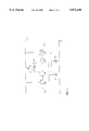
- FIG. 1 is a schematic diagram of a transconductance circuit
- FIG. 2 is a schematic diagram of a Gilbert Cell Core
- FIG. 3 is a schematic diagram of a novel analog multiplier circuit constructed according to the invention.
- the novel multiplier uses one transconductance circuit (FIG. 1) to generate a compensating bias voltage for a Gilbert Cell core (FIG. 2).
- An understanding of how the transconductance circuit and the Gilbert Cell core operate is useful in understanding how these two circuit elements can be used together to achieve a novel multiplier having the desired characteristics set forth above.
- devices M3 and M4 have the same dimensions.
- Devices M1 and M2 also have the same dimensions, however, devices M3 and M4 are scaled by a size factor n relative to devices M1 and M2.
- Current sources IA and IB are both set to (n+1) I, where n is the scale factor described above.
- the input to the circuit (V x+ and V x- ) is the same as the "x" input to the Gilbert Cell core which will be described later.
- the signal plus dc drain currents of M1 and M2 are summed (I tran ) in device M5.
- I tran The equation for I tran , can be written as a function of the differential input voltage V x . All devices are biased to operate in the saturation region. The resulting expression is given in terms of the scale factor n, the dc current I, the circuit transconductance coefficient K tran and the differential input voltage V x . The current I tran is used to bias the Gilbert Cell core multiplier. ##EQU2##
- I is a fixed DC current and is equal to IA/IB divided by n+1 where n is the scale factor described above.
- FIG. 2 A conventional Gillbert Cell core used as a multiplier (V x *V y ) is illustrated in FIG. 2.
- current sources IC and ID can be either fixed or compensated to overcome the non-linearities discussed above.
- I tran current (a function of V x ) developed in the transconductance circuit of FIG. 1 is used in lieu of conventional current sources IC and ID.
- I tran is applied via a current mirror illustrated in FIG. 3 (see devices M12-M15) to compensate for the operating conditions described above which in the absence of compensation would introduce non-linearties.
- the Gilbert Cell multiplier illustrated in FIG. 2 has two cross-coupled n-channel differential pairs M6-M9 (matched transistors), equal resistive loads R1 and R2 and a folded p-channel pair M10 and M11.
- the four n-channel transistors are of equal dimensions and the two p-channel transistors are of equal dimensions.
- current sources IC and ID are equal and are generated from the I tran output of the transconductance circuit illustrated in FIG. 1.
- Equation 3 can be re-written ##EQU4##
- the terms under the radical include V x squared as does I tran , therefore the term can be eliminated.
- V x squared terms By expanding the current I tran in terms of n and V x1 the dependence on V x for the term under the radical can be eliminated with the proper value for n.
- K tran the transconductance circuit device transconductance coefficient
- K n Gilbert Cell device transconductance coefficient
- R refers to the value in ohms of the Gilbert Cell load resistors R1 and R2.
- equation 10 represents an ideal multiplication operation and is valid as long as the devices remain in saturation.
- FIG. 3 is a schematic of a complete multiplier.
- the references employed in FIG. 3 are the same as those used in FIGS. 1 and 2 in those cases where the element performs the same function in the circuit illustrated in FIG. 3.
- V x and V y are applied as illustrated in FIG. 3 to devices M6-M9 and M10-M11, respectively of the Gibert Cell core.
- V x is applied to devices M1-M4 of the transconductance circuit which converts V x to related current (I tran ). This current mirrored by transistors M12 and M13 to current sources M14 and M15 which replace current sources IC and ID illustrated in FIG. 2.
Abstract
A low voltage CMOS multiplier uses a transconductance stage to generate a dynamic bias current which is used to compensate for non-linear terms in a Gilbert Cell multiplier circuit. Common mode dependence is minimized by using balanced differential input stages for both the transconductance and multiplier stages.
Description
The invention relates to analog signal multipliers and more specifically to a low voltage, four-quadrant CMOS analog multiplier with dynamic bias compensation to achieve accurate linear operation over a wide differential input voltage range and having a low sensitivity to common mode voltage at either input.
Analog multipliers are used in many different applications such as modulators, demodulators and mixers to name a few. In some applications it is necessary that the multiplier yield linear products of both inputs. Linear products of both inputs are easily achieved in the digital domain. However, the results can involve considerable cost over an analog implementation in the form of A/D and D/A converters and in general consume more power and chip area than an analog implementation.
The most critical design specification for a multiplier is linearity or distortion for a given dynamic voltage range, either input or output. If the input voltages are small, a simple MOS version of the well known Gilbert cell can be used with good results. If larger input ranges are contemplated, a compensation technique must be employed in order to improve linearity at the extremes of the range. Furthermore, low voltage supplies require additional techniques, such as folding, to make linear operation possible with standard CMOS devices. The use of a compensation signal without encountering increased common mode signal dependence and the use of many additional devices is difficult at best. In addition, operation using standard CMOS devices at low supply voltages (3.3 V) presents a unique challenge.
The publications listed below are considered relevant background material since alternative solutions or components include in the application.
1. Garverick, Sodini, "A Wide-Band NMOS Balanced Modulator/Amplifier Which Uses 1 um Transistors for Linearity," IEEE Journal of Solid-State Circuits, Vol. 23, No. 1, p. 195, February 1988.
2. Pena-Finol and Connely, "A MOS Four-Quadrant Analog Multiplier Using the Quarter-Square Technique," IEEE Journal of Solid State Circuits, Vol. SC-20, No. 6, p. 1158, December 1985.
3. Z. Wang, "A CMOS Four-Quadrant Analog Multiplier with Single-Ended Voltage Output and Improved Temperature Performance," IEEE Journal of Solid State Circuits, Vol. 26, No. 9, p. 1293, September 1991.
4. Babanezhad and Temes, "A 20V Four-Quadrant CMOS Analog Mulitplier," IEEE Journal of Solid-State Circuits, Vol. SC-20, No. 6, p. 1158, December 1985.
5. Wong, Kalyanasundaram, Salam, "Wide Dynamic Range Four-Quadrant CMOS Analog Multiplier Using Linearized Transconductance Stages," IEEE Journal Solid State Circuits, Vol. SC-21, No. 6, p. 1120, December 1986.
6. Nedungadi and Viswanathan, "Design of Linear CMOS Transconductance Elements," IEEE Transactions on Circuits Systems, Vol. CAS-31, p. 891, October, 1984.
7. B. Gilbert, "A Precise Four-Quadrant Multiplier with Subnanosecond Response," IEEE Journal Solid State Circuits, Vol. SC-3, No. 4, December, 1968.
(1) uses the linear transconductance properties of short channel devices to construct a multiplier. This solution is not acceptable due to the reliability problems associated with high fields and short channel devices.
(2) and (3) disclose a quarter-square technique which uses the square of the sum of the input signals minus the square of the difference of the input signals, to obtain a linearly scaled product of the two inputs.
(4) and (5) disclose a compensated Gilbert Cell discussed above.
(6) describes a transconductance stage, a component used in this invention.
(7) describes a simple MOS version of a Gilbert Cell, a component used in the invention and described above.
The invention contemplates a circuit for multiplying two signals represented by two analog voltages Vx and Vy. A transconductance circuit responsive to Vx converts Vx to a related first current Itran. Two n-channel cross coupled differential transistor pairs of a Gilbert Cell core multiplier responsive to Vx provide a second currents Ix and Iy which are related to the value of Vx ; a folded p-channel transistor pair responsive to Vy provide a third currents Iy1 and Iy2 related to Vy ; and, a current source under control of the first current combines the second and third currents whereby the voltage output of the Gibert Cell core is a linear representation of the product of Vx and Vy.
FIG. 1 is a schematic diagram of a transconductance circuit;
FIG. 2 is a schematic diagram of a Gilbert Cell Core; and,
FIG. 3 is a schematic diagram of a novel analog multiplier circuit constructed according to the invention.
The novel multiplier (FIG. 3) uses one transconductance circuit (FIG. 1) to generate a compensating bias voltage for a Gilbert Cell core (FIG. 2). An understanding of how the transconductance circuit and the Gilbert Cell core operate is useful in understanding how these two circuit elements can be used together to achieve a novel multiplier having the desired characteristics set forth above.
In FIG. 1 devices M3 and M4 have the same dimensions. Devices M1 and M2 also have the same dimensions, however, devices M3 and M4 are scaled by a size factor n relative to devices M1 and M2. Current sources IA and IB are both set to (n+1) I, where n is the scale factor described above. The input to the circuit (Vx+ and Vx-) is the same as the "x" input to the Gilbert Cell core which will be described later. The signal plus dc drain currents of M1 and M2 are summed (Itran) in device M5.
Based on the (ideal) square-law behavior of the MOS transistor in saturation ##EQU1##
The equation for Itran, can be written as a function of the differential input voltage Vx. All devices are biased to operate in the saturation region. The resulting expression is given in terms of the scale factor n, the dc current I, the circuit transconductance coefficient Ktran and the differential input voltage Vx. The current Itran is used to bias the Gilbert Cell core multiplier. ##EQU2##
I is a fixed DC current and is equal to IA/IB divided by n+1 where n is the scale factor described above.
A conventional Gillbert Cell core used as a multiplier (Vx *Vy) is illustrated in FIG. 2. In the prior art, current sources IC and ID can be either fixed or compensated to overcome the non-linearities discussed above. In the discussion which follows it will be assumed that the Itran current (a function of Vx) developed in the transconductance circuit of FIG. 1 is used in lieu of conventional current sources IC and ID. Itran is applied via a current mirror illustrated in FIG. 3 (see devices M12-M15) to compensate for the operating conditions described above which in the absence of compensation would introduce non-linearties.
The Gilbert Cell multiplier illustrated in FIG. 2 has two cross-coupled n-channel differential pairs M6-M9 (matched transistors), equal resistive loads R1 and R2 and a folded p-channel pair M10 and M11. The four n-channel transistors are of equal dimensions and the two p-channel transistors are of equal dimensions. In the analysis it will be assumed that current sources IC and ID are equal and are generated from the Itran output of the transconductance circuit illustrated in FIG. 1.
The output (Vout) from the cross coupled pairs (M6-M9) is ##EQU3## where Ix and Iy are illustrated in FIG. 2 and Kn is the device transconductance coefficient of transistors M6-M9. When all of the devices are in saturation, current sources Ix and Iy can be expressed as a function of Itran and the current Iy1 and Iy2 from the folded p=channel transistors M10 and M11, respectively.
I.sub.x =I.sub.tran -I.sub.y1
I.sub.y =I.sub.tran -I.sub.y2 (4)
By substitution, equation 3 can be re-written ##EQU4## The terms under the radical include Vx squared as does Itran, therefore the term can be eliminated. By expanding the current Itran in terms of n and Vx1 the dependence on Vx for the term under the radical can be eliminated with the proper value for n. For Vx squared terms to be eliminated: ##EQU5## By setting Ktran (the transconductance circuit device transconductance coefficient) equal to Kn (Gilbert Cell device transconductance coefficient) and selecting n as ##EQU6## the expression for Vout reduces to: ##EQU7## R refers to the value in ohms of the Gilbert Cell load resistors R1 and R2. For IE=21, where IE is the dc bias tail current for the p-channel "Y" input pair: ##EQU8## this can by written in terms of Vy : ##EQU9##
equation 10 represents an ideal multiplication operation and is valid as long as the devices remain in saturation.
FIG. 3 is a schematic of a complete multiplier. The references employed in FIG. 3 are the same as those used in FIGS. 1 and 2 in those cases where the element performs the same function in the circuit illustrated in FIG. 3. Vx and Vy are applied as illustrated in FIG. 3 to devices M6-M9 and M10-M11, respectively of the Gibert Cell core. Vx is applied to devices M1-M4 of the transconductance circuit which converts Vx to related current (Itran). This current mirrored by transistors M12 and M13 to current sources M14 and M15 which replace current sources IC and ID illustrated in FIG. 2.
Claims (5)
1. A circuit for multiplying two signals represented by two analog voltages Vx and Vy comprising:
a transconductance circuit responsive to Vx for converting Vx to a related first current (Itran); and,
a Gilbert Cell core multiplier having two n-channel cross coupled differential transistor pairs responsive to said voltage Vx and providing a second current (Ix, Iy) related to the value of Vx, a folded p-channel transistor pair responsive to the voltage Vy and providing a third current (Iy1, Iy2) related to the voltage Vy, and a current source (M14,M15) under control of said first current for combining said second and third currents whereby the voltage output (Vout) of the said Gibert Cell core is a linear representation of the product of Vx and Vy.
2. The multiplier set forth in claim 1 in which the signal voltage Vx is a differential voltage (Vx+ and Vx-) and the transconductance circuit responsive to the differential voltage includes:
a first pair of transistors (M3 and M4) each responsive to a different phase of the differential signal voltage;
a second pair of transistors (M1 and M2) each responsive to a different phase of the differential signal voltage;
said first pair being scaled by a size factor n relative to the second pair; and,
circuit means including a current source for connecting the two pairs between a bias voltage and ground.
3. The multiplier circuit set forth in claim 2 in which the transconductance coefficients of the transistors in the transconductance circuit are set equal to a predetermined ratio of the transconductance coefficients of the transistors in the Gilbert Cell.
4. The multiplier circuit set forth in claim 3 in which the predetermined ratio is one.
5. The multiplier set forth in claim 4 in which the scale factor n is set equal to 1+2/√3.
Priority Applications (1)
| Application Number | Priority Date | Filing Date | Title |
|---|---|---|---|
| US08/910,165 US5872446A (en) | 1997-08-12 | 1997-08-12 | Low voltage CMOS analog multiplier with extended input dynamic range |
Applications Claiming Priority (1)
| Application Number | Priority Date | Filing Date | Title |
|---|---|---|---|
| US08/910,165 US5872446A (en) | 1997-08-12 | 1997-08-12 | Low voltage CMOS analog multiplier with extended input dynamic range |
Publications (1)
| Publication Number | Publication Date |
|---|---|
| US5872446A true US5872446A (en) | 1999-02-16 |
Family
ID=25428398
Family Applications (1)
| Application Number | Title | Priority Date | Filing Date |
|---|---|---|---|
| US08/910,165 Expired - Fee Related US5872446A (en) | 1997-08-12 | 1997-08-12 | Low voltage CMOS analog multiplier with extended input dynamic range |
Country Status (1)
| Country | Link |
|---|---|
| US (1) | US5872446A (en) |
Cited By (50)
| Publication number | Priority date | Publication date | Assignee | Title |
|---|---|---|---|---|
| US6266518B1 (en) | 1998-10-21 | 2001-07-24 | Parkervision, Inc. | Method and system for down-converting electromagnetic signals by sampling and integrating over apertures |
| US6300845B1 (en) * | 2000-04-06 | 2001-10-09 | Linear Technology Corporation | Low-voltage, current-folded signal modulators and methods |
| US20010038318A1 (en) * | 1999-11-24 | 2001-11-08 | Parker Vision, Inc. | Phased array antenna applications for universal frequency translation |
| US6330274B1 (en) | 1998-09-08 | 2001-12-11 | University Of Hawaii | Spread-spectrum continous-time analog correlator and method therefor |
| US6370371B1 (en) | 1998-10-21 | 2002-04-09 | Parkervision, Inc. | Applications of universal frequency translation |
| US20020042257A1 (en) * | 2000-04-14 | 2002-04-11 | Sorrells David F. | Apparatus, system, and method for down-converting and up-converting electromagnetic signals |
| US20020049038A1 (en) * | 2000-01-28 | 2002-04-25 | Sorrells David F. | Wireless and wired cable modem applications of universal frequency translation technology |
| FR2818828A1 (en) * | 2000-12-22 | 2002-06-28 | St Microelectronics Sa | Device for frequency transposition of radio signal by mixing with local oscillator signal, for use in transmitters and receivers of radio-communication apparatus |
| US6421534B1 (en) | 1998-10-21 | 2002-07-16 | Parkervision, Inc. | Integrated frequency translation and selectivity |
| US6433720B1 (en) | 2001-03-06 | 2002-08-13 | Furaxa, Inc. | Methods, apparatuses, and systems for sampling or pulse generation |
| US20020124036A1 (en) * | 2000-11-14 | 2002-09-05 | Parkervision, Inc. | Method and apparatus for a parallel correlator and applications thereof |
| US6489816B1 (en) | 2001-09-07 | 2002-12-03 | Signia Technologies | Frequency converter with direct current suppression |
| FR2827097A1 (en) * | 2001-07-05 | 2003-01-10 | Zarlink Semiconductor Ltd | High frequency mixer with image rejection circuit having transconductance circuit two feed wires placed providing input signal and switching stage with central MOS mixer between transconductance circuit/load. |
| WO2003005561A2 (en) * | 2001-07-06 | 2003-01-16 | Infineon Technologies Ag | Interface circuit for connecting to an output of a frequency converter |
| US20030022640A1 (en) * | 1999-08-23 | 2003-01-30 | Parker Vision, Inc. | Method and system for frequency up-conversion |
| US20030048212A1 (en) * | 2001-06-06 | 2003-03-13 | Libove Joel M. | Methods and apparatuses for multiple sampling and multiple pulse generation |
| US6542722B1 (en) | 1998-10-21 | 2003-04-01 | Parkervision, Inc. | Method and system for frequency up-conversion with variety of transmitter configurations |
| US6542019B1 (en) | 2001-11-28 | 2003-04-01 | Berkäna Wireless, Inc. | Highly linear and low noise figure mixer |
| US6560301B1 (en) | 1998-10-21 | 2003-05-06 | Parkervision, Inc. | Integrated frequency translation and selectivity with a variety of filter embodiments |
| US6590432B1 (en) * | 2002-09-26 | 2003-07-08 | Pericom Semiconductor Corp. | Low-voltage differential driver with opened eye pattern |
| US6647250B1 (en) | 1998-10-21 | 2003-11-11 | Parkervision, Inc. | Method and system for ensuring reception of a communications signal |
| US20030222702A1 (en) * | 2002-04-04 | 2003-12-04 | Christian Bjork | Quadrature switching mixer with reduced leakage |
| US20040002321A1 (en) * | 1999-04-16 | 2004-01-01 | Parker Vision, Inc. | Method and apparatus for reducing re-radiation using techniques of universal frequency translation technology |
| US20040013177A1 (en) * | 2002-07-18 | 2004-01-22 | Parker Vision, Inc. | Networking methods and systems |
| US20040015420A1 (en) * | 2002-07-18 | 2004-01-22 | Sorrells David F. | Networking methods and systems |
| US6694128B1 (en) | 1998-08-18 | 2004-02-17 | Parkervision, Inc. | Frequency synthesizer using universal frequency translation technology |
| US6704558B1 (en) | 1999-01-22 | 2004-03-09 | Parkervision, Inc. | Image-reject down-converter and embodiments thereof, such as the family radio service |
| US6704549B1 (en) | 1999-03-03 | 2004-03-09 | Parkvision, Inc. | Multi-mode, multi-band communication system |
| US20040176064A1 (en) * | 2002-04-04 | 2004-09-09 | Sven Mattisson | Mixer with feedback |
| US6791371B1 (en) | 2003-03-27 | 2004-09-14 | Pericom Semiconductor Corp. | Power-down activated by differential-input multiplier and comparator |
| US6794918B1 (en) * | 2003-03-27 | 2004-09-21 | Applied Micro Circuits Corporation | Loop-back clock phase generator |
| US6813485B2 (en) | 1998-10-21 | 2004-11-02 | Parkervision, Inc. | Method and system for down-converting and up-converting an electromagnetic signal, and transforms for same |
| US20050024038A1 (en) * | 2003-07-31 | 2005-02-03 | John Santhoff | Sampling circuit apparatus and method |
| US20050035663A1 (en) * | 2003-07-31 | 2005-02-17 | Steven Moore | Electromagnetic pulse generator |
| US20050035660A1 (en) * | 2003-07-31 | 2005-02-17 | John Santhoff | Electromagnetic pulse generator |
| US20050100115A1 (en) * | 1999-04-16 | 2005-05-12 | Sorrells David F. | Method, system, and apparatus for balanced frequency Up-conversion of a baseband signal |
| US20050111346A1 (en) * | 2003-11-25 | 2005-05-26 | John Santhoff | Bridged ultra-wideband communication method and apparatus |
| US20050173767A1 (en) * | 2001-12-25 | 2005-08-11 | Atsushi Hirabayashi | Multiplier |
| US20050243709A1 (en) * | 2003-11-21 | 2005-11-03 | John Santhoff | Bridged ultra-wideband communication method and apparatus |
| US20090075610A1 (en) * | 2006-05-19 | 2009-03-19 | California Institute Of Technology | Digital and analog im3 product compensation circuits for an rf receiver |
| US7653145B2 (en) | 1999-08-04 | 2010-01-26 | Parkervision, Inc. | Wireless local area network (WLAN) using universal frequency translation technology including multi-phase embodiments and circuit implementations |
| US7653158B2 (en) | 2001-11-09 | 2010-01-26 | Parkervision, Inc. | Gain control in a communication channel |
| US7693230B2 (en) | 1999-04-16 | 2010-04-06 | Parkervision, Inc. | Apparatus and method of differential IQ frequency up-conversion |
| US7724845B2 (en) | 1999-04-16 | 2010-05-25 | Parkervision, Inc. | Method and system for down-converting and electromagnetic signal, and transforms for same |
| US7865177B2 (en) | 1998-10-21 | 2011-01-04 | Parkervision, Inc. | Method and system for down-converting an electromagnetic signal, and transforms for same, and aperture relationships |
| US7991815B2 (en) | 2000-11-14 | 2011-08-02 | Parkervision, Inc. | Methods, systems, and computer program products for parallel correlation and applications thereof |
| US8233855B2 (en) | 1998-10-21 | 2012-07-31 | Parkervision, Inc. | Up-conversion based on gated information signal |
| US8295406B1 (en) | 1999-08-04 | 2012-10-23 | Parkervision, Inc. | Universal platform module for a plurality of communication protocols |
| WO2016119661A1 (en) * | 2015-01-27 | 2016-08-04 | 意瑞半导体(上海)有限公司 | Power factor correction circuit and multiplier |
| US10218324B2 (en) * | 2016-12-30 | 2019-02-26 | Texas Instruments Incorporated | Differential input stage with wide input signal range and stable transconductance |
Citations (9)
| Publication number | Priority date | Publication date | Assignee | Title |
|---|---|---|---|---|
| US4546275A (en) * | 1983-06-02 | 1985-10-08 | Georgia Tech Research Institute | Quarter-square analog four-quadrant multiplier using MOS integrated circuit technology |
| US5115409A (en) * | 1988-08-31 | 1992-05-19 | Siemens Aktiengesellschaft | Multiple-input four-quadrant multiplier |
| US5182477A (en) * | 1990-03-22 | 1993-01-26 | Silicon Systems, Inc. | Bipolar tunable transconductance element |
| US5298796A (en) * | 1992-07-08 | 1994-03-29 | The United States Of America As Represented By The Administrator Of The National Aeronautics And Space Administration | Nonvolatile programmable neural network synaptic array |
| US5442583A (en) * | 1993-05-14 | 1995-08-15 | California Institute Of Technology | Compensated analog multipliers |
| US5523717A (en) * | 1993-11-10 | 1996-06-04 | Nec Corporation | Operational transconductance amplifier and Bi-MOS multiplier |
| US5570056A (en) * | 1995-06-07 | 1996-10-29 | Pacific Communication Sciences, Inc. | Bipolar analog multipliers for low voltage applications |
| US5587687A (en) * | 1995-02-02 | 1996-12-24 | Silicon Systems, Inc. | Multiplier based transconductance amplifiers and transconductance control circuits |
| US5635863A (en) * | 1995-05-25 | 1997-06-03 | Vtc, Inc. | Programmable phase comparator |
-
1997
- 1997-08-12 US US08/910,165 patent/US5872446A/en not_active Expired - Fee Related
Patent Citations (9)
| Publication number | Priority date | Publication date | Assignee | Title |
|---|---|---|---|---|
| US4546275A (en) * | 1983-06-02 | 1985-10-08 | Georgia Tech Research Institute | Quarter-square analog four-quadrant multiplier using MOS integrated circuit technology |
| US5115409A (en) * | 1988-08-31 | 1992-05-19 | Siemens Aktiengesellschaft | Multiple-input four-quadrant multiplier |
| US5182477A (en) * | 1990-03-22 | 1993-01-26 | Silicon Systems, Inc. | Bipolar tunable transconductance element |
| US5298796A (en) * | 1992-07-08 | 1994-03-29 | The United States Of America As Represented By The Administrator Of The National Aeronautics And Space Administration | Nonvolatile programmable neural network synaptic array |
| US5442583A (en) * | 1993-05-14 | 1995-08-15 | California Institute Of Technology | Compensated analog multipliers |
| US5523717A (en) * | 1993-11-10 | 1996-06-04 | Nec Corporation | Operational transconductance amplifier and Bi-MOS multiplier |
| US5587687A (en) * | 1995-02-02 | 1996-12-24 | Silicon Systems, Inc. | Multiplier based transconductance amplifiers and transconductance control circuits |
| US5635863A (en) * | 1995-05-25 | 1997-06-03 | Vtc, Inc. | Programmable phase comparator |
| US5570056A (en) * | 1995-06-07 | 1996-10-29 | Pacific Communication Sciences, Inc. | Bipolar analog multipliers for low voltage applications |
Cited By (101)
| Publication number | Priority date | Publication date | Assignee | Title |
|---|---|---|---|---|
| US6694128B1 (en) | 1998-08-18 | 2004-02-17 | Parkervision, Inc. | Frequency synthesizer using universal frequency translation technology |
| US6330274B1 (en) | 1998-09-08 | 2001-12-11 | University Of Hawaii | Spread-spectrum continous-time analog correlator and method therefor |
| US6798351B1 (en) | 1998-10-21 | 2004-09-28 | Parkervision, Inc. | Automated meter reader applications of universal frequency translation |
| US6687493B1 (en) | 1998-10-21 | 2004-02-03 | Parkervision, Inc. | Method and circuit for down-converting a signal using a complementary FET structure for improved dynamic range |
| US20060141975A1 (en) * | 1998-10-21 | 2006-06-29 | Parkervision, Inc. | Methods and systems for down-converting a signal using a complementary transistor structure |
| US20050272395A1 (en) * | 1998-10-21 | 2005-12-08 | Parkervision, Inc. | Method and circuit for down-converting a signal |
| US7697916B2 (en) | 1998-10-21 | 2010-04-13 | Parkervision, Inc. | Applications of universal frequency translation |
| US6266518B1 (en) | 1998-10-21 | 2001-07-24 | Parkervision, Inc. | Method and system for down-converting electromagnetic signals by sampling and integrating over apertures |
| US6421534B1 (en) | 1998-10-21 | 2002-07-16 | Parkervision, Inc. | Integrated frequency translation and selectivity |
| US8340618B2 (en) | 1998-10-21 | 2012-12-25 | Parkervision, Inc. | Method and system for down-converting an electromagnetic signal, and transforms for same, and aperture relationships |
| US7826817B2 (en) | 1998-10-21 | 2010-11-02 | Parker Vision, Inc. | Applications of universal frequency translation |
| US20020160809A1 (en) * | 1998-10-21 | 2002-10-31 | Parker Vision, Inc. | Applications of universal frequency translation |
| US7865177B2 (en) | 1998-10-21 | 2011-01-04 | Parkervision, Inc. | Method and system for down-converting an electromagnetic signal, and transforms for same, and aperture relationships |
| US8233855B2 (en) | 1998-10-21 | 2012-07-31 | Parkervision, Inc. | Up-conversion based on gated information signal |
| US6836650B2 (en) | 1998-10-21 | 2004-12-28 | Parkervision, Inc. | Methods and systems for down-converting electromagnetic signals, and applications thereof |
| US6813485B2 (en) | 1998-10-21 | 2004-11-02 | Parkervision, Inc. | Method and system for down-converting and up-converting an electromagnetic signal, and transforms for same |
| US6370371B1 (en) | 1998-10-21 | 2002-04-09 | Parkervision, Inc. | Applications of universal frequency translation |
| US7937059B2 (en) | 1998-10-21 | 2011-05-03 | Parkervision, Inc. | Converting an electromagnetic signal via sub-sampling |
| US7693502B2 (en) | 1998-10-21 | 2010-04-06 | Parkervision, Inc. | Method and system for down-converting an electromagnetic signal, transforms for same, and aperture relationships |
| US20030068990A1 (en) * | 1998-10-21 | 2003-04-10 | Parkervision, Inc. | Method and system for frequency up-conversion with a variety of transmitter configurations |
| US6560301B1 (en) | 1998-10-21 | 2003-05-06 | Parkervision, Inc. | Integrated frequency translation and selectivity with a variety of filter embodiments |
| US8190116B2 (en) | 1998-10-21 | 2012-05-29 | Parker Vision, Inc. | Methods and systems for down-converting a signal using a complementary transistor structure |
| US6580902B1 (en) | 1998-10-21 | 2003-06-17 | Parkervision, Inc. | Frequency translation using optimized switch structures |
| US20030112895A1 (en) * | 1998-10-21 | 2003-06-19 | Parkervision, Inc. | Intergrated frequency translation and selectivity |
| US8190108B2 (en) | 1998-10-21 | 2012-05-29 | Parkervision, Inc. | Method and system for frequency up-conversion |
| US20030186670A1 (en) * | 1998-10-21 | 2003-10-02 | Sorrells David F. | Method and circuit or down-converting a signal |
| US8160534B2 (en) | 1998-10-21 | 2012-04-17 | Parkervision, Inc. | Applications of universal frequency translation |
| US6647250B1 (en) | 1998-10-21 | 2003-11-11 | Parkervision, Inc. | Method and system for ensuring reception of a communications signal |
| US7936022B2 (en) | 1998-10-21 | 2011-05-03 | Parkervision, Inc. | Method and circuit for down-converting a signal |
| US6542722B1 (en) | 1998-10-21 | 2003-04-01 | Parkervision, Inc. | Method and system for frequency up-conversion with variety of transmitter configurations |
| US8019291B2 (en) | 1998-10-21 | 2011-09-13 | Parkervision, Inc. | Method and system for frequency down-conversion and frequency up-conversion |
| US6704558B1 (en) | 1999-01-22 | 2004-03-09 | Parkervision, Inc. | Image-reject down-converter and embodiments thereof, such as the family radio service |
| US6704549B1 (en) | 1999-03-03 | 2004-03-09 | Parkvision, Inc. | Multi-mode, multi-band communication system |
| US8229023B2 (en) | 1999-04-16 | 2012-07-24 | Parkervision, Inc. | Wireless local area network (WLAN) using universal frequency translation technology including multi-phase embodiments |
| US8036304B2 (en) | 1999-04-16 | 2011-10-11 | Parkervision, Inc. | Apparatus and method of differential IQ frequency up-conversion |
| US20040002321A1 (en) * | 1999-04-16 | 2004-01-01 | Parker Vision, Inc. | Method and apparatus for reducing re-radiation using techniques of universal frequency translation technology |
| US8077797B2 (en) | 1999-04-16 | 2011-12-13 | Parkervision, Inc. | Method, system, and apparatus for balanced frequency up-conversion of a baseband signal |
| US8223898B2 (en) | 1999-04-16 | 2012-07-17 | Parkervision, Inc. | Method and system for down-converting an electromagnetic signal, and transforms for same |
| US7929638B2 (en) | 1999-04-16 | 2011-04-19 | Parkervision, Inc. | Wireless local area network (WLAN) using universal frequency translation technology including multi-phase embodiments |
| US8224281B2 (en) | 1999-04-16 | 2012-07-17 | Parkervision, Inc. | Down-conversion of an electromagnetic signal with feedback control |
| US7773688B2 (en) | 1999-04-16 | 2010-08-10 | Parkervision, Inc. | Method, system, and apparatus for balanced frequency up-conversion, including circuitry to directly couple the outputs of multiple transistors |
| US20050100115A1 (en) * | 1999-04-16 | 2005-05-12 | Sorrells David F. | Method, system, and apparatus for balanced frequency Up-conversion of a baseband signal |
| US7894789B2 (en) | 1999-04-16 | 2011-02-22 | Parkervision, Inc. | Down-conversion of an electromagnetic signal with feedback control |
| US7693230B2 (en) | 1999-04-16 | 2010-04-06 | Parkervision, Inc. | Apparatus and method of differential IQ frequency up-conversion |
| US8594228B2 (en) | 1999-04-16 | 2013-11-26 | Parkervision, Inc. | Apparatus and method of differential IQ frequency up-conversion |
| US7724845B2 (en) | 1999-04-16 | 2010-05-25 | Parkervision, Inc. | Method and system for down-converting and electromagnetic signal, and transforms for same |
| US8295406B1 (en) | 1999-08-04 | 2012-10-23 | Parkervision, Inc. | Universal platform module for a plurality of communication protocols |
| US7653145B2 (en) | 1999-08-04 | 2010-01-26 | Parkervision, Inc. | Wireless local area network (WLAN) using universal frequency translation technology including multi-phase embodiments and circuit implementations |
| US20030022640A1 (en) * | 1999-08-23 | 2003-01-30 | Parker Vision, Inc. | Method and system for frequency up-conversion |
| US20070224950A1 (en) * | 1999-08-23 | 2007-09-27 | Parkervision, Inc. | Method and system for frequency up-conversion |
| US20010038318A1 (en) * | 1999-11-24 | 2001-11-08 | Parker Vision, Inc. | Phased array antenna applications for universal frequency translation |
| US20020049038A1 (en) * | 2000-01-28 | 2002-04-25 | Sorrells David F. | Wireless and wired cable modem applications of universal frequency translation technology |
| US6300845B1 (en) * | 2000-04-06 | 2001-10-09 | Linear Technology Corporation | Low-voltage, current-folded signal modulators and methods |
| US7822401B2 (en) | 2000-04-14 | 2010-10-26 | Parkervision, Inc. | Apparatus and method for down-converting electromagnetic signals by controlled charging and discharging of a capacitor |
| US20050085208A1 (en) * | 2000-04-14 | 2005-04-21 | Parkervision, Inc. | Apparatus, system, and method for down-converting and up-converting electromagnetic signals |
| US20050227639A1 (en) * | 2000-04-14 | 2005-10-13 | Parkervision, Inc. | Apparatus, system, and method for down converting and up converting electromagnetic signals |
| US20050085207A1 (en) * | 2000-04-14 | 2005-04-21 | Parkervision, Inc. | Apparatus, system, and method for down-converting and up-converting electromagnetic signals |
| US20020042257A1 (en) * | 2000-04-14 | 2002-04-11 | Sorrells David F. | Apparatus, system, and method for down-converting and up-converting electromagnetic signals |
| US8295800B2 (en) | 2000-04-14 | 2012-10-23 | Parkervision, Inc. | Apparatus and method for down-converting electromagnetic signals by controlled charging and discharging of a capacitor |
| US20050193049A1 (en) * | 2000-11-14 | 2005-09-01 | Parkervision, Inc. | Method and apparatus for a parallel correlator and applications thereof |
| US20020124036A1 (en) * | 2000-11-14 | 2002-09-05 | Parkervision, Inc. | Method and apparatus for a parallel correlator and applications thereof |
| US7991815B2 (en) | 2000-11-14 | 2011-08-02 | Parkervision, Inc. | Methods, systems, and computer program products for parallel correlation and applications thereof |
| FR2818828A1 (en) * | 2000-12-22 | 2002-06-28 | St Microelectronics Sa | Device for frequency transposition of radio signal by mixing with local oscillator signal, for use in transmitters and receivers of radio-communication apparatus |
| US6433720B1 (en) | 2001-03-06 | 2002-08-13 | Furaxa, Inc. | Methods, apparatuses, and systems for sampling or pulse generation |
| US6642878B2 (en) | 2001-06-06 | 2003-11-04 | Furaxa, Inc. | Methods and apparatuses for multiple sampling and multiple pulse generation |
| US20030048212A1 (en) * | 2001-06-06 | 2003-03-13 | Libove Joel M. | Methods and apparatuses for multiple sampling and multiple pulse generation |
| FR2827097A1 (en) * | 2001-07-05 | 2003-01-10 | Zarlink Semiconductor Ltd | High frequency mixer with image rejection circuit having transconductance circuit two feed wires placed providing input signal and switching stage with central MOS mixer between transconductance circuit/load. |
| WO2003005561A3 (en) * | 2001-07-06 | 2003-05-30 | Infineon Technologies Ag | Interface circuit for connecting to an output of a frequency converter |
| US7126424B2 (en) | 2001-07-06 | 2006-10-24 | Infineon Technologies Inc. | Interface circuit for connecting to an output of a frequency converter |
| WO2003005561A2 (en) * | 2001-07-06 | 2003-01-16 | Infineon Technologies Ag | Interface circuit for connecting to an output of a frequency converter |
| US6489816B1 (en) | 2001-09-07 | 2002-12-03 | Signia Technologies | Frequency converter with direct current suppression |
| US7653158B2 (en) | 2001-11-09 | 2010-01-26 | Parkervision, Inc. | Gain control in a communication channel |
| US8446994B2 (en) | 2001-11-09 | 2013-05-21 | Parkervision, Inc. | Gain control in a communication channel |
| US6542019B1 (en) | 2001-11-28 | 2003-04-01 | Berkäna Wireless, Inc. | Highly linear and low noise figure mixer |
| US20050173767A1 (en) * | 2001-12-25 | 2005-08-11 | Atsushi Hirabayashi | Multiplier |
| US7321253B2 (en) * | 2001-12-25 | 2008-01-22 | Sony Corporation | Multiplier |
| US7672659B2 (en) | 2002-04-04 | 2010-03-02 | Telefonaktiebolaget L M Ericsson (Publ) | Mixer with feedback |
| US20030222702A1 (en) * | 2002-04-04 | 2003-12-04 | Christian Bjork | Quadrature switching mixer with reduced leakage |
| US20040176064A1 (en) * | 2002-04-04 | 2004-09-09 | Sven Mattisson | Mixer with feedback |
| US20040015420A1 (en) * | 2002-07-18 | 2004-01-22 | Sorrells David F. | Networking methods and systems |
| US8407061B2 (en) | 2002-07-18 | 2013-03-26 | Parkervision, Inc. | Networking methods and systems |
| US20040013177A1 (en) * | 2002-07-18 | 2004-01-22 | Parker Vision, Inc. | Networking methods and systems |
| US8160196B2 (en) | 2002-07-18 | 2012-04-17 | Parkervision, Inc. | Networking methods and systems |
| US6590432B1 (en) * | 2002-09-26 | 2003-07-08 | Pericom Semiconductor Corp. | Low-voltage differential driver with opened eye pattern |
| US6791371B1 (en) | 2003-03-27 | 2004-09-14 | Pericom Semiconductor Corp. | Power-down activated by differential-input multiplier and comparator |
| US6794918B1 (en) * | 2003-03-27 | 2004-09-21 | Applied Micro Circuits Corporation | Loop-back clock phase generator |
| US20070110204A1 (en) * | 2003-07-31 | 2007-05-17 | John Santhoff | Sampling circuit apparatus and method |
| US20050035663A1 (en) * | 2003-07-31 | 2005-02-17 | Steven Moore | Electromagnetic pulse generator |
| US20050035660A1 (en) * | 2003-07-31 | 2005-02-17 | John Santhoff | Electromagnetic pulse generator |
| US20050024038A1 (en) * | 2003-07-31 | 2005-02-03 | John Santhoff | Sampling circuit apparatus and method |
| US20050260952A1 (en) * | 2003-11-21 | 2005-11-24 | John Santhoff | Bridged ultra-wideband communication method and apparatus |
| US20050243709A1 (en) * | 2003-11-21 | 2005-11-03 | John Santhoff | Bridged ultra-wideband communication method and apparatus |
| US7046618B2 (en) | 2003-11-25 | 2006-05-16 | Pulse-Link, Inc. | Bridged ultra-wideband communication method and apparatus |
| US20050111346A1 (en) * | 2003-11-25 | 2005-05-26 | John Santhoff | Bridged ultra-wideband communication method and apparatus |
| US7894788B2 (en) | 2006-05-19 | 2011-02-22 | California Institute Of Technology | Digital and analog IM3 product compensation circuits for an RF receiver |
| US20110110473A1 (en) * | 2006-05-19 | 2011-05-12 | Edward Keehr | Digital and analog im3 product compensation circuits for an rf receiver |
| US20090075610A1 (en) * | 2006-05-19 | 2009-03-19 | California Institute Of Technology | Digital and analog im3 product compensation circuits for an rf receiver |
| US8971834B2 (en) | 2006-05-19 | 2015-03-03 | California Institute Of Technology | Digital and analog IM3 product compensation circuits for an RF receiver |
| WO2016119661A1 (en) * | 2015-01-27 | 2016-08-04 | 意瑞半导体(上海)有限公司 | Power factor correction circuit and multiplier |
| US10171035B2 (en) | 2015-01-27 | 2019-01-01 | Cosemitech (Shanghai) Co., Ltd. | Power factor correction circuit and multiplier |
| US10218324B2 (en) * | 2016-12-30 | 2019-02-26 | Texas Instruments Incorporated | Differential input stage with wide input signal range and stable transconductance |
Similar Documents
| Publication | Publication Date | Title |
|---|---|---|
| US5872446A (en) | Low voltage CMOS analog multiplier with extended input dynamic range | |
| US6788146B2 (en) | Capacitor compensation in miller compensated circuits | |
| US4829266A (en) | CMOS power operational amplifier | |
| KR100326878B1 (en) | Amplification circuit | |
| US5497123A (en) | Amplifier circuit having high linearity for cancelling third order harmonic distortion | |
| EP1006648B1 (en) | Active compensating capacitive multiplier | |
| US5929621A (en) | Generation of temperature compensated low noise symmetrical reference voltages | |
| US6118340A (en) | Low noise differential input, differential output amplifier and method | |
| JPH0786850A (en) | Perfect differential operational amplifier and same phase reconstruction in differential operational amplifier | |
| JPH0629761A (en) | Differential amplifier provided with reinforced in-phase mode stability | |
| US7295068B2 (en) | Increasing the linearity of a transconductance cell | |
| US4835487A (en) | MOS voltage to current converter | |
| US4720686A (en) | Circuit for converting a fully differential amplifier to a single-ended output amplifier | |
| US6121818A (en) | Mixer using replica voltage-current converter | |
| JP3486072B2 (en) | Variable gain amplifier | |
| US5113148A (en) | Linear CMOS output stage | |
| KR100302936B1 (en) | Differential amplifier | |
| US6437631B2 (en) | Analog multiplying circuit and variable gain amplifying circuit | |
| JP3081210B2 (en) | Linear gain amplifier | |
| US5424681A (en) | Wide range operational amplifier | |
| JPH06232655A (en) | Single end differential converter | |
| US4761615A (en) | Voltage repeater circuit with low harmonic distortion for loads with a resistive component | |
| US6191622B1 (en) | Time interleaved common mode feedback circuit with process compensated bias | |
| Ramirez-Angulo | Highly linear four quadrant analog BiCMOS multiplier for/spl plusmn/1.5 V supply operation | |
| US20050052216A1 (en) | Logarithmic linear variable gain CMOS amplifier |
Legal Events
| Date | Code | Title | Description |
|---|---|---|---|
| AS | Assignment |
Owner name: INTERNATIONAL BUSINESS MACHINES CORPORATION, NEW Y Free format text: ASSIGNMENT OF ASSIGNORS INTEREST;ASSIGNORS:CRANFOR, HAYDEN C.;GYURCSIK, RONALD S., JR.;MCELWEE, JAMES F., JR.;REEL/FRAME:009237/0012;SIGNING DATES FROM 19970812 TO 19970826 |
|
| REMI | Maintenance fee reminder mailed | ||
| LAPS | Lapse for failure to pay maintenance fees | ||
| FP | Lapsed due to failure to pay maintenance fee |
Effective date: 20030216 |
|
| STCH | Information on status: patent discontinuation |
Free format text: PATENT EXPIRED DUE TO NONPAYMENT OF MAINTENANCE FEES UNDER 37 CFR 1.362 |