US5905303A - Method for manufacturing bump leaded film carrier type semiconductor device - Google Patents
Method for manufacturing bump leaded film carrier type semiconductor device Download PDFInfo
- Publication number
- US5905303A US5905303A US08/873,593 US87359397A US5905303A US 5905303 A US5905303 A US 5905303A US 87359397 A US87359397 A US 87359397A US 5905303 A US5905303 A US 5905303A
- Authority
- US
- United States
- Prior art keywords
- conductive layers
- openings
- pads
- insulating film
- semiconductor chip
- Prior art date
- Legal status (The legal status is an assumption and is not a legal conclusion. Google has not performed a legal analysis and makes no representation as to the accuracy of the status listed.)
- Expired - Lifetime
Links
- 239000004065 semiconductor Substances 0.000 title claims abstract description 76
- 238000004519 manufacturing process Methods 0.000 title description 17
- 238000000034 method Methods 0.000 title description 9
- 239000010410 layer Substances 0.000 claims abstract description 86
- 239000012790 adhesive layer Substances 0.000 claims abstract description 15
- 229920005989 resin Polymers 0.000 claims description 38
- 239000011347 resin Substances 0.000 claims description 38
- 239000000945 filler Substances 0.000 claims description 16
- 238000002161 passivation Methods 0.000 claims description 10
- 238000001721 transfer moulding Methods 0.000 claims description 7
- 238000004382 potting Methods 0.000 claims description 4
- 229910000679 solder Inorganic materials 0.000 description 17
- 229910052751 metal Inorganic materials 0.000 description 13
- 239000002184 metal Substances 0.000 description 13
- 239000002390 adhesive tape Substances 0.000 description 11
- 239000000758 substrate Substances 0.000 description 11
- 229920005992 thermoplastic resin Polymers 0.000 description 7
- 239000010931 gold Substances 0.000 description 6
- 238000007789 sealing Methods 0.000 description 6
- 239000000853 adhesive Substances 0.000 description 5
- 230000001070 adhesive effect Effects 0.000 description 5
- 238000005530 etching Methods 0.000 description 5
- 229920001721 polyimide Polymers 0.000 description 5
- 230000008569 process Effects 0.000 description 5
- 238000012360 testing method Methods 0.000 description 5
- 239000004642 Polyimide Substances 0.000 description 4
- 238000002347 injection Methods 0.000 description 4
- 239000007924 injection Substances 0.000 description 4
- 239000007788 liquid Substances 0.000 description 4
- 230000004048 modification Effects 0.000 description 4
- 238000012986 modification Methods 0.000 description 4
- XUIMIQQOPSSXEZ-UHFFFAOYSA-N Silicon Chemical compound [Si] XUIMIQQOPSSXEZ-UHFFFAOYSA-N 0.000 description 3
- 230000008901 benefit Effects 0.000 description 3
- 229920002313 fluoropolymer Polymers 0.000 description 3
- 229910052737 gold Inorganic materials 0.000 description 3
- 238000010438 heat treatment Methods 0.000 description 3
- 238000007747 plating Methods 0.000 description 3
- 229910052710 silicon Inorganic materials 0.000 description 3
- 239000010703 silicon Substances 0.000 description 3
- 229920001187 thermosetting polymer Polymers 0.000 description 3
- 239000004593 Epoxy Substances 0.000 description 2
- 239000011248 coating agent Substances 0.000 description 2
- 238000000576 coating method Methods 0.000 description 2
- 229910052802 copper Inorganic materials 0.000 description 2
- 238000005520 cutting process Methods 0.000 description 2
- 230000000694 effects Effects 0.000 description 2
- 230000004907 flux Effects 0.000 description 2
- PCHJSUWPFVWCPO-UHFFFAOYSA-N gold Chemical compound [Au] PCHJSUWPFVWCPO-UHFFFAOYSA-N 0.000 description 2
- 239000000463 material Substances 0.000 description 2
- 229910052759 nickel Inorganic materials 0.000 description 2
- 239000011368 organic material Substances 0.000 description 2
- 238000000206 photolithography Methods 0.000 description 2
- 238000012546 transfer Methods 0.000 description 2
- 239000011800 void material Substances 0.000 description 2
- 206010067482 No adverse event Diseases 0.000 description 1
- 229910052581 Si3N4 Inorganic materials 0.000 description 1
- VYPSYNLAJGMNEJ-UHFFFAOYSA-N Silicium dioxide Chemical compound O=[Si]=O VYPSYNLAJGMNEJ-UHFFFAOYSA-N 0.000 description 1
- ATJFFYVFTNAWJD-UHFFFAOYSA-N Tin Chemical compound [Sn] ATJFFYVFTNAWJD-UHFFFAOYSA-N 0.000 description 1
- 239000002313 adhesive film Substances 0.000 description 1
- 239000004840 adhesive resin Substances 0.000 description 1
- 229920006223 adhesive resin Polymers 0.000 description 1
- 229910045601 alloy Inorganic materials 0.000 description 1
- 239000000956 alloy Substances 0.000 description 1
- 230000005260 alpha ray Effects 0.000 description 1
- 229910052782 aluminium Inorganic materials 0.000 description 1
- XAGFODPZIPBFFR-UHFFFAOYSA-N aluminium Chemical compound [Al] XAGFODPZIPBFFR-UHFFFAOYSA-N 0.000 description 1
- 125000003118 aryl group Chemical group 0.000 description 1
- 230000004888 barrier function Effects 0.000 description 1
- 230000015572 biosynthetic process Effects 0.000 description 1
- 239000000969 carrier Substances 0.000 description 1
- 239000000919 ceramic Substances 0.000 description 1
- 229910052804 chromium Inorganic materials 0.000 description 1
- 238000004140 cleaning Methods 0.000 description 1
- 230000008878 coupling Effects 0.000 description 1
- 238000010168 coupling process Methods 0.000 description 1
- 238000005859 coupling reaction Methods 0.000 description 1
- 238000005336 cracking Methods 0.000 description 1
- 230000002542 deteriorative effect Effects 0.000 description 1
- 238000009792 diffusion process Methods 0.000 description 1
- 230000003628 erosive effect Effects 0.000 description 1
- 238000001704 evaporation Methods 0.000 description 1
- 239000011888 foil Substances 0.000 description 1
- 230000009477 glass transition Effects 0.000 description 1
- 230000017525 heat dissipation Effects 0.000 description 1
- 229910052738 indium Inorganic materials 0.000 description 1
- APFVFJFRJDLVQX-UHFFFAOYSA-N indium atom Chemical compound [In] APFVFJFRJDLVQX-UHFFFAOYSA-N 0.000 description 1
- 238000003780 insertion Methods 0.000 description 1
- 230000037431 insertion Effects 0.000 description 1
- 238000009413 insulation Methods 0.000 description 1
- 230000010354 integration Effects 0.000 description 1
- 238000002844 melting Methods 0.000 description 1
- 230000008018 melting Effects 0.000 description 1
- 230000003287 optical effect Effects 0.000 description 1
- 229910052763 palladium Inorganic materials 0.000 description 1
- 229920000642 polymer Polymers 0.000 description 1
- 238000003825 pressing Methods 0.000 description 1
- 230000002265 prevention Effects 0.000 description 1
- 229910052703 rhodium Inorganic materials 0.000 description 1
- HQVNEWCFYHHQES-UHFFFAOYSA-N silicon nitride Chemical compound N12[Si]34N5[Si]62N3[Si]51N64 HQVNEWCFYHHQES-UHFFFAOYSA-N 0.000 description 1
- 229910052814 silicon oxide Inorganic materials 0.000 description 1
- 238000004544 sputter deposition Methods 0.000 description 1
- 238000005728 strengthening Methods 0.000 description 1
- 229920001169 thermoplastic Polymers 0.000 description 1
- 239000004416 thermosoftening plastic Substances 0.000 description 1
Images


Classifications
-
- H—ELECTRICITY
- H01—ELECTRIC ELEMENTS
- H01L—SEMICONDUCTOR DEVICES NOT COVERED BY CLASS H10
- H01L23/00—Details of semiconductor or other solid state devices
- H01L23/48—Arrangements for conducting electric current to or from the solid state body in operation, e.g. leads, terminal arrangements ; Selection of materials therefor
- H01L23/488—Arrangements for conducting electric current to or from the solid state body in operation, e.g. leads, terminal arrangements ; Selection of materials therefor consisting of soldered or bonded constructions
- H01L23/498—Leads, i.e. metallisations or lead-frames on insulating substrates, e.g. chip carriers
- H01L23/4985—Flexible insulating substrates
-
- H—ELECTRICITY
- H01—ELECTRIC ELEMENTS
- H01L—SEMICONDUCTOR DEVICES NOT COVERED BY CLASS H10
- H01L21/00—Processes or apparatus adapted for the manufacture or treatment of semiconductor or solid state devices or of parts thereof
- H01L21/02—Manufacture or treatment of semiconductor devices or of parts thereof
- H01L21/04—Manufacture or treatment of semiconductor devices or of parts thereof the devices having at least one potential-jump barrier or surface barrier, e.g. PN junction, depletion layer or carrier concentration layer
- H01L21/50—Assembly of semiconductor devices using processes or apparatus not provided for in a single one of the subgroups H01L21/06 - H01L21/326, e.g. sealing of a cap to a base of a container
- H01L21/60—Attaching or detaching leads or other conductive members, to be used for carrying current to or from the device in operation
-
- H—ELECTRICITY
- H01—ELECTRIC ELEMENTS
- H01L—SEMICONDUCTOR DEVICES NOT COVERED BY CLASS H10
- H01L23/00—Details of semiconductor or other solid state devices
- H01L23/28—Encapsulations, e.g. encapsulating layers, coatings, e.g. for protection
- H01L23/31—Encapsulations, e.g. encapsulating layers, coatings, e.g. for protection characterised by the arrangement or shape
- H01L23/3107—Encapsulations, e.g. encapsulating layers, coatings, e.g. for protection characterised by the arrangement or shape the device being completely enclosed
-
- H—ELECTRICITY
- H01—ELECTRIC ELEMENTS
- H01L—SEMICONDUCTOR DEVICES NOT COVERED BY CLASS H10
- H01L2224/00—Indexing scheme for arrangements for connecting or disconnecting semiconductor or solid-state bodies and methods related thereto as covered by H01L24/00
- H01L2224/01—Means for bonding being attached to, or being formed on, the surface to be connected, e.g. chip-to-package, die-attach, "first-level" interconnects; Manufacturing methods related thereto
- H01L2224/10—Bump connectors; Manufacturing methods related thereto
- H01L2224/15—Structure, shape, material or disposition of the bump connectors after the connecting process
- H01L2224/16—Structure, shape, material or disposition of the bump connectors after the connecting process of an individual bump connector
- H01L2224/161—Disposition
- H01L2224/16151—Disposition the bump connector connecting between a semiconductor or solid-state body and an item not being a semiconductor or solid-state body, e.g. chip-to-substrate, chip-to-passive
- H01L2224/16221—Disposition the bump connector connecting between a semiconductor or solid-state body and an item not being a semiconductor or solid-state body, e.g. chip-to-substrate, chip-to-passive the body and the item being stacked
- H01L2224/16225—Disposition the bump connector connecting between a semiconductor or solid-state body and an item not being a semiconductor or solid-state body, e.g. chip-to-substrate, chip-to-passive the body and the item being stacked the item being non-metallic, e.g. insulating substrate with or without metallisation
-
- H—ELECTRICITY
- H01—ELECTRIC ELEMENTS
- H01L—SEMICONDUCTOR DEVICES NOT COVERED BY CLASS H10
- H01L2224/00—Indexing scheme for arrangements for connecting or disconnecting semiconductor or solid-state bodies and methods related thereto as covered by H01L24/00
- H01L2224/01—Means for bonding being attached to, or being formed on, the surface to be connected, e.g. chip-to-package, die-attach, "first-level" interconnects; Manufacturing methods related thereto
- H01L2224/26—Layer connectors, e.g. plate connectors, solder or adhesive layers; Manufacturing methods related thereto
- H01L2224/31—Structure, shape, material or disposition of the layer connectors after the connecting process
- H01L2224/32—Structure, shape, material or disposition of the layer connectors after the connecting process of an individual layer connector
- H01L2224/321—Disposition
- H01L2224/32151—Disposition the layer connector connecting between a semiconductor or solid-state body and an item not being a semiconductor or solid-state body, e.g. chip-to-substrate, chip-to-passive
- H01L2224/32221—Disposition the layer connector connecting between a semiconductor or solid-state body and an item not being a semiconductor or solid-state body, e.g. chip-to-substrate, chip-to-passive the body and the item being stacked
- H01L2224/32225—Disposition the layer connector connecting between a semiconductor or solid-state body and an item not being a semiconductor or solid-state body, e.g. chip-to-substrate, chip-to-passive the body and the item being stacked the item being non-metallic, e.g. insulating substrate with or without metallisation
-
- H—ELECTRICITY
- H01—ELECTRIC ELEMENTS
- H01L—SEMICONDUCTOR DEVICES NOT COVERED BY CLASS H10
- H01L2224/00—Indexing scheme for arrangements for connecting or disconnecting semiconductor or solid-state bodies and methods related thereto as covered by H01L24/00
- H01L2224/73—Means for bonding being of different types provided for in two or more of groups H01L2224/10, H01L2224/18, H01L2224/26, H01L2224/34, H01L2224/42, H01L2224/50, H01L2224/63, H01L2224/71
- H01L2224/732—Location after the connecting process
- H01L2224/73201—Location after the connecting process on the same surface
- H01L2224/73203—Bump and layer connectors
- H01L2224/73204—Bump and layer connectors the bump connector being embedded into the layer connector
-
- H—ELECTRICITY
- H01—ELECTRIC ELEMENTS
- H01L—SEMICONDUCTOR DEVICES NOT COVERED BY CLASS H10
- H01L2224/00—Indexing scheme for arrangements for connecting or disconnecting semiconductor or solid-state bodies and methods related thereto as covered by H01L24/00
- H01L2224/80—Methods for connecting semiconductor or other solid state bodies using means for bonding being attached to, or being formed on, the surface to be connected
- H01L2224/83—Methods for connecting semiconductor or other solid state bodies using means for bonding being attached to, or being formed on, the surface to be connected using a layer connector
- H01L2224/8319—Arrangement of the layer connectors prior to mounting
- H01L2224/83191—Arrangement of the layer connectors prior to mounting wherein the layer connectors are disposed only on the semiconductor or solid-state body
-
- H—ELECTRICITY
- H01—ELECTRIC ELEMENTS
- H01L—SEMICONDUCTOR DEVICES NOT COVERED BY CLASS H10
- H01L2924/00—Indexing scheme for arrangements or methods for connecting or disconnecting semiconductor or solid-state bodies as covered by H01L24/00
- H01L2924/01—Chemical elements
- H01L2924/01046—Palladium [Pd]
-
- H—ELECTRICITY
- H01—ELECTRIC ELEMENTS
- H01L—SEMICONDUCTOR DEVICES NOT COVERED BY CLASS H10
- H01L2924/00—Indexing scheme for arrangements or methods for connecting or disconnecting semiconductor or solid-state bodies as covered by H01L24/00
- H01L2924/01—Chemical elements
- H01L2924/01078—Platinum [Pt]
-
- H—ELECTRICITY
- H01—ELECTRIC ELEMENTS
- H01L—SEMICONDUCTOR DEVICES NOT COVERED BY CLASS H10
- H01L2924/00—Indexing scheme for arrangements or methods for connecting or disconnecting semiconductor or solid-state bodies as covered by H01L24/00
- H01L2924/01—Chemical elements
- H01L2924/01079—Gold [Au]
-
- H—ELECTRICITY
- H01—ELECTRIC ELEMENTS
- H01L—SEMICONDUCTOR DEVICES NOT COVERED BY CLASS H10
- H01L2924/00—Indexing scheme for arrangements or methods for connecting or disconnecting semiconductor or solid-state bodies as covered by H01L24/00
- H01L2924/15—Details of package parts other than the semiconductor or other solid state devices to be connected
- H01L2924/151—Die mounting substrate
- H01L2924/1515—Shape
- H01L2924/15151—Shape the die mounting substrate comprising an aperture, e.g. for underfilling, outgassing, window type wire connections
-
- H—ELECTRICITY
- H01—ELECTRIC ELEMENTS
- H01L—SEMICONDUCTOR DEVICES NOT COVERED BY CLASS H10
- H01L2924/00—Indexing scheme for arrangements or methods for connecting or disconnecting semiconductor or solid-state bodies as covered by H01L24/00
- H01L2924/15—Details of package parts other than the semiconductor or other solid state devices to be connected
- H01L2924/151—Die mounting substrate
- H01L2924/1517—Multilayer substrate
- H01L2924/15172—Fan-out arrangement of the internal vias
- H01L2924/15173—Fan-out arrangement of the internal vias in a single layer of the multilayer substrate
-
- H—ELECTRICITY
- H01—ELECTRIC ELEMENTS
- H01L—SEMICONDUCTOR DEVICES NOT COVERED BY CLASS H10
- H01L2924/00—Indexing scheme for arrangements or methods for connecting or disconnecting semiconductor or solid-state bodies as covered by H01L24/00
- H01L2924/15—Details of package parts other than the semiconductor or other solid state devices to be connected
- H01L2924/151—Die mounting substrate
- H01L2924/153—Connection portion
- H01L2924/1531—Connection portion the connection portion being formed only on the surface of the substrate opposite to the die mounting surface
- H01L2924/15311—Connection portion the connection portion being formed only on the surface of the substrate opposite to the die mounting surface being a ball array, e.g. BGA
-
- H—ELECTRICITY
- H01—ELECTRIC ELEMENTS
- H01L—SEMICONDUCTOR DEVICES NOT COVERED BY CLASS H10
- H01L2924/00—Indexing scheme for arrangements or methods for connecting or disconnecting semiconductor or solid-state bodies as covered by H01L24/00
- H01L2924/30—Technical effects
- H01L2924/301—Electrical effects
- H01L2924/3025—Electromagnetic shielding
-
- Y—GENERAL TAGGING OF NEW TECHNOLOGICAL DEVELOPMENTS; GENERAL TAGGING OF CROSS-SECTIONAL TECHNOLOGIES SPANNING OVER SEVERAL SECTIONS OF THE IPC; TECHNICAL SUBJECTS COVERED BY FORMER USPC CROSS-REFERENCE ART COLLECTIONS [XRACs] AND DIGESTS
- Y10—TECHNICAL SUBJECTS COVERED BY FORMER USPC
- Y10T—TECHNICAL SUBJECTS COVERED BY FORMER US CLASSIFICATION
- Y10T29/00—Metal working
- Y10T29/49—Method of mechanical manufacture
- Y10T29/49002—Electrical device making
- Y10T29/49117—Conductor or circuit manufacturing
- Y10T29/49121—Beam lead frame or beam lead device
Definitions
- the present invention relates to a method for manufacturing a bump leaded film carrier type semiconductor device.
- New semiconductor packages have been developed to correspond to requirements of electronic apparatuses which are of a smaller size, of a smaller weight, of a higher speed and of a higher function.
- TAB tape automated bonding
- One typical area array bonding system is a flip-chip bonding system.
- solder bumps are formed on an active element surface of a chip, and then, the chip is reversed and is bonded directly to a substrate, thus corresponding to multi-pins and small-pitched pins.
- the length of bonded connections is so short that there is an advantage in high speed and low noise.
- a process for forming barrier metal and bumps on electrode pads of a bare chip is generally required.
- solder is applied as bump material for aluminum electrodes, Cr or Ti as an adhesive layer and Cu
- Ni, Rh or Pd as a diffusion avoiding layer have to be formed on electrode faces by a sputtering method or an evaporation method.
- a step for forming bumps made of solder or Au by ball bumps or by plating is required.
- a transfer bump system or mesa bump system for bonding bumps formed on inner leads has been suggested.
- outer leads i.e., portions of leads connected to a substrate extend to the outside, and as a result, there is a disadvantage in size.
- an insulating film has conductive layers on a first surface and conductive protrusions on a second surface.
- the conductive layers are connected to the conductive protrusions via through holes provided in the insulating film.
- a semiconductor chip having pads is adhered by an adhesive layer to the insulating film.
- the conductive layers are locally pressured, so that the conductive layers are electrically connected to respective ones of the pads.
- the device can be made firm by the combination of the semiconductor chip and the insulating film using the adhesive layer. Simultaneously, since the adhesive layer can be thin, the device can be small in size.
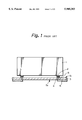
- FIG. 1 is a cross-sectional view illustrating a first prior art bump leaded film carrier type semiconductor device
- FIGS. 2A and 2B are cross-sectional views illustrating a modification of the device of FIG. 1;
- FIG. 5A is a cross-sectional view illustrating a first embodiment of the bump leaded film carrier type semiconductor device according to the present invention
- FIG. 5B is a bottom view of the device of FIG. 5A;
- FIG. 6A is a plan view of a film carrier for explaining the manufacturing steps of the device of FIG. 5A;
- FIG. 6B is a bottom view of the film carrier of FIG. 6A;
- FIGS. 7A through 7H are cross-sectional views for explaining the manufacturing steps of the device of FIG. 5A;
- FIG. 8 is a partially-enlarged cross-sectional view of the device of FIG. 7C;
- FIG. 9A is a cross-sectional view illustrating a second embodiment of the bump leaded film carrier type semiconductor device according to the present invention.
- FIG. 9B is a bottom view of the device of FIG. 9A;
- FIG. 10A is a plan view of a film carrier for explaining the manufacturing steps of the device of FIG. 9A;
- FIG. 10B is a bottom view of the film carrier of FIG. 9A;
- FIGS. 11A through 11H are cross-sectional views for explaining the manufacturing steps of the device of FIG. 9A;
- FIG. 12 is a partially-enlarged cross-sectional view of the device of FIG. 11C;
- FIG. 13A is a cross-sectional view illustrating a third embodiment of the bump leaded film carrier type semiconductor device according to the present invention.
- FIG. 13B is a bottom view of the device of FIG. 13A;
- FIG. 14A is a cross-sectional view illustrating a fourth embodiment of the bump leaded film carrier type semiconductor device according to the present invention.
- FIG. 14B is a bottom view of the device of FIG. 14A;
- FIG. 15A is a cross-sectional view illustrating a fifth embodiment of the bump leaded film carrier type semiconductor device according to the present invention.
- FIG. 15B is a bottom view of the device of FIG. 15A;
- FIG. 16A is a plan view of the insulating film of FIGS. 13A, 13B, 14A, 14B, 15A and 15B;
- FIG. 16B is a bottom view of the insulating film of FIGS. 13A, 13B, 14A, 14B, 15A and 15B;
- FIG. 17A is a cross-sectional view illustrating a sixth embodiment of the bump leaded film carrier type semiconductor device according to the present invention.
- FIGS. 18A through 18G are cross-sectional views for explaining the manufacturing steps of the device of FIG. 17A;
- FIG. 19 is a cross-sectional view illustrating a seventh embodiment of the bump leaded film carrier type semiconductor device according to the present invention.
- FIGS. 20A and 20B are cross-sectional views illustrating an eighth embodiment of the bump leaded film carrier type semiconductor device according to the present invention.
- FIG. 20C is a bottom view of the device of FIGS. 20A and 20B.
- FIG. 1 which illustrates a first prior art bump leaded film carrier type semiconductor device (see: JP-A-SHO53-56969, JP-A-HEI5-47847), reference numeral 1 designates a bare chip having pads 2. Also, reference numeral 3 designates an insulating film made of polyimide or the like. Throughholes are perforated by a photolithography and etching process or a pressing process in the insulating film 3, and conductive members 4 are fitted into the through holes. Also, conductive protrusions, i.e., bumps 5 coupled to the conductive members 4 are provided on a first surface S1 of the insulating film 3. On the other hand, conductive layers 6 coupled to the conductive members 4 are provided on a second surface S2 of the insulating film 3.
- outer leads (not shown) of the conductive layers 6 are located outside of the chip 1, which increases the device of FIG. 1 in size. Also, since the support of the chip 1 to the insulating film 3 is carried out by only the bonding of the pads 2 to the bumps 5, the mechanical strength of the device is deteriorated.
- FIG. 3 which illustrates a second prior art bump leaded film carrier type semiconductor device (see: JP-A-HEI4-154136)
- bumps are provided instead of the outer leads of FIGS. 1, 2A and 2B. That is, the conductive layers 6 are provided on the first surface S1 of the insulating film 3, and bumps 9 coupled to the conductive members 4 are provided on the second surface S 2 of the insulating film 3.
- an area array bonding system can be adopted.
- the device of FIG. 3 is advantageous in size.
- FIG. 4 which is a modification of the device of FIG. 3 (see: JP-A-HEI5-82586), transfer molding using resin is introduced to improve the contact characteristics of the chip 1 to the insulating film 3. That is, the chip 1 is entirely covered by resin indicated by reference numeral 10. In this case, in order to effectively transfer molding, other bumps 11 are added to the pads 2, thus enlarging a gap between the chip 1 and the insulating film 3.
- FIG. 5A is a cross-sectional view illustrating a first embodiment of the bump leaded film carrier type semiconductor device according to the present invention
- FIG. 5B is a bottom view of the device of FIG. 5A.
- FIG. 5A is a cross-sectional view taken along the line A--A of FIG. 5B.
- the conductive layers 6 are formed on the first surface S 1 of the insulating film 3.
- the bumps 9 made of solder are provided on the second surface S 2 of the insulating film 3.
- the bumps 9 are arranged in a grid having the same pitch, thus realizing an area array bonding system.
- FIGS. 5A and 5B The manufacturing steps of the semiconductor device of FIGS. 5A and 5B are explained next with reference to FIGS. 6A and 6B, 7A through 7H, and 8.
- FIGS. 6A and 6B a film carrier 30 as illustrated in FIGS. 6A and 6B is prepared.
- FIG. 6A shows a conductive pattern side (first surface) of the film carrier 30, and
- FIG. 6B shows a substrate side (second surface) of the film carrier 30.
- a conductive pattern 60 including the conductive layers 6 and test pads 601 is formed by using a photolithography and etching process on the first surface S1 of the film carrier 30.
- the openings 21 and the through holes for the conductive members 4 are perforated by laser or etching in the film carrier 30.
- the conductive members 4 are fitted into the through holes.
- the conductive members 4 are made of Au, Ni or Cu, preferably, Cu, since Au is expensive and Ni is easily cracked.
- the conductive members 4 can be positively protruded on the horizontal direction on the second surface S 2 of the film carrier 30, to increase the land diameter of the bumps 9, thus strengthening the mechanical contact characteristics therebetween.
- a single point bonding system is used to carry out a bonding of inner leads, i.e., to bond the chip 1 to the film carrier 30.
- the single point bonding system using heat and ultrasonic waves has better heat transfer characteristics than a gang bonding system. That is, the Cu component of the conductive layers 6 of the conductive pattern 60 and the Al component of the pads 2 form alloy so that the conductive layers 6 are firmly bonded to the pads 2 of the chip 1.
- reference numeral 23 designates a bonding tool whose weight and operational time are controlled in accordance with the width of the conductive layer 6 and the like. Also, ultrasonic waves can be used for operating the bonding tool 23.
- a test is carried out by supplying electrical signals to the test pads 601 of the conductive pattern 60.
- the periphery of the chip 1 is cut by using a metal die (not shown). For example, a cutting operation is carried out in view of a 100 ⁇ m edge allowance, however, it is possible to carry out a precise cutting operation by laser or dicing. Thus, the insulating film 3 is left.
- the bumps 9 made of solder are formed on the conductive members 4.
- balls are formed by using a wire bonding method on a wire made by solder, and the balls are bonded on the conductive members 4. After that, the wire is cut so that the balls are left to form the bumps 9.
- bump forming material indium capable of low temperature bonding can be used instead of solder. Further, the formation of the bumps is carried out at a step for preparing the film carrier 30 as illustrated in FIGS. 6A and 6B.
- the device of FIG. 7G is provisionally mounted on a mounting substrate 24 by using a high precision mounter (not shown).
- the solder bumps 9 are aligned with lands 24a of the mounting substrate 24 by using an optical system, and a weight is applied with heating, to carry out a provisional nounting of the device. After that, a proper bonding is carried out in a reflow furnace.
- the pitch of pads for the outer leads is preferably about 0.5 in view of the mounting characteristics.
- solder is also formed on mounting substrate 24, it is possible to increase the distance between the insulating film 3 and the substrate 24.
- FIG. 9A is a cross-sectional view illustrating a second embodiment of the bump leaded film carrier type semiconductor device according to the present invention
- FIG. 9B is a bottom view of the device of FIG. 9A.
- FIG. 9A is a cross-sectional view taken along the line A--A of FIG. 9B.
- through holes 31 are provided in the insulating film 3 instead of the openings 21 of FIGS. 5A and 5B.
- Fillers 32 made of metal are fitted into the through holes 31. Therefore, when bonding inner leads by a bonding tool, the bonding tool can easily push each of the conductive layers 6 via a respective one of the fillers 32.
- the through hole 31 can be precisely formed in alignment with the pads 2 of the chip 1 and the conductive layers 6. Further, the mechanical strength in the inner lead portions can be strengthened. Still further, since energy is transmitted effectively from the fillers 32 to the inner lead portions, the bonding condition of the inner leads can be relaxed.
- FIGS. 10A and 10B 11A through 11H, and 12, which correspond to FIGS. 6A and 6B, 7A through 7H, and 8, respectively.
- the through holes 31 and the fillers 32 therein are provided instead of the openings 21 of FIGS. 6A and 6B.
- the through holes 31 formed by laser or an etching process have to be in alignment with the conductive layers 6.
- the pads 2 are arranged at a pitch of 100 ⁇ m on the chip 1, the pitch of the through holes 31 is also 100 ⁇ m.
- the width of the conductive layers 6 is as large as possible in view of the alignment with the through holes 31.
- the width of the conductive layers 6 is as small as possible in view of the prevention of short circuits around the conductive member 4 (or the bumps 9) in a grid.
- the through holes 31 are 50 ⁇ m in diameter.
- the film carrier 30 is as thin as possible.
- a single point bonding system is adopted, which is different from those as shown in FIGS. 7A through 7H.
- the single point bonding system is shown in detail in FIGS. 11C and 12. That is, a bonding tool 23 is provided for each of the fillers 32, i.e., each of the conductive layers 6. Also, in this case, the surface of the chip 1 is heated up to about 300° C.
- FIG. 13A is a cross-sectional view illustrating a third embodiment of the bump leaded film carrier type semiconductor device according to the present invention
- FIG. 13B is a bottom view of the device of FIG. 13A.
- FIG. 13A is a cross-sectional view taken along the line A--A of FIG. 13B.
- the conductive layers 6 are provided on the second surface S 2 of the insulating film 3.
- parts of the conductive layers 6 extend via the through holes 31 to the first surface S 1 of the insulating film 3 and correspond to the pads 2 of the chip 1
- the conductive layers 6 on the first surface S 1 is etched to form pads 6a corresponding to the pads 2.
- the part of the conductive layers 6 in the through holes 31 can be formed by plating.
- a cover 41 made of resin or polyimide is coated on the conductive layers 6 on the side of the second surface S 2 , to electrically protect the conductive layers 6.
- FIG. 14A is a cross-sectional view illustrating a fourth embodiment of the bump leaded film carrier type semiconductor device according to the present invention
- FIG. 14B is a bottom view of the device of FIG. 14A.
- FIG. 14A is a cross-sectional view taken along the line A--A of FIG. 14B.
- the fourth embodiment is similar to the third embodiment.
- FIGS. 14A and 14B fillers 42 made of metal are inserted between the pads 2 and the conductive layers 6, to easily push the conductive layers 6 by the bonding tool 23' (see FIG. 12).
- the metal fillers 42 can be easily formed by solder bumps using a solder bump system. Therefore, the metal fillers 42 are advantageous in shear strength as compared with the parts 6a of the conductive layers 6 of the third embodiment.
- FIG. 15A is a cross-sectional view illustrating a fifth embodiment of the bump leaded film carrier type semiconductor device according to the present invention
- FIG. 15B is a bottom view of the device of FIG. 15A.
- FIG. 15A is a cross-sectional view taken along the line A--A of FIG. 15B.
- the fifth embodiment is similar to the fourth embodiment. That is, in FIGS. 15A and 15B, metal fillers 43 are positively protruded along the horizontal direction on the first surface S1 of the insulating film 3. As a result, the thickness of the insulating film 3 can be reduced more in the fifth embodiment than in the fourth embodiment, thus reducing the device in size.
- FIGS. 16A and 16B show a film carrier 30 used for manufacturing the devices of FIGS. 13A, 13B, 14A, 14B, 15A and 15B.
- FIG. 16A shows a chip side surface (first surface) of the film carrier 30, and
- FIG. 16B shows a conductive pattern side (second surface) of the film carrier 30. Since the conductive layers 6 are located on the second surface S 2 of the film carrier 30, the cover 41 covers the conductive layers 6 except for the inner lead portions and the test pads 601 thereof, which is different from the film carriers as shown in FIGS. 5A, 5B, 10A and 10B.
- the adhesive (tape) layer 22 can be made of thermosetting resin or thermoplastic resin.
- Thermoplastic polyimid is polymer coupled by imid coupling of aromatic molecules, so that a heat resistance of higher than 400° C. is obtained Also, the mutual interruption of molecules of the thermoplastic resin is weak, and therefore, the thermoplastic resin has thermal flowability. Also, the glass transition temperature of the thermoplastic resin for defining the thermal flowability can be arbitrarily controlled. Thus, thermoplastic resin rather than thermosetting resin is preferable for the adhesive (tape) layer 22. Further, since a bonding between the chip 1 and the insulating film 3 is carried out at a low temperature and a low pressure, thermoplastic resin is preferable. However, other heat-resistant adhesive film and thermosetting polyimide capable of high speed curing can be used as the adhesive (tape) layer 22.
- the size of the adhesive layer 22 should be smaller than that of the chip 1
- the adhesive layer 22 is as thin as possible, to reduce a step between the chip 1 and the insulating film 3.
- the adhesive layer 22 is preferably about 10 to 30 ⁇ m.
- the flexible insulating film 3 is interposed between the chip 1 and the substrate 24, a stress generated due to the difference in thermal expansibility rate therebetween can be relaxed.
- a height of about 100 ⁇ m is required and insertion of liquid resin into gaps is indispensable, while, in the above-described embodiments, since the height after bonding can be smaller than about 50 ⁇ m, the diameter of the bumps 9 can be smaller than about 80 ⁇ m in diameter in view of the warpage of the substrate 24.
- FIG. 17A is a cross-sectional view illustrating a sixth embodiment of the bump leaded film carrier type semiconductor device according to the present invention
- FIG. 17B is a bottom view of the device of FIG. 17A.
- FIG. 17A is a cross-sectional view taken along the line A--A of FIG. 17B.
- a resin injection opening 3a is perforated at a center of the insulating film 3 of FIGS. 9A and 9B. That is, liquid resin is injected via the resin injection opening 3a into a gap between the chip 1 and the insulating film 3, to thereby form a resin layer 51 instead of the adhesive layer 22 of FIGS. 9A and 9B.
- FIGS. 17A and 17B The manufacturing steps of the semiconductor device of FIGS. 17A and 17B are explained next with reference to FIGS. 18A through 18G which correspond to FIGS. 11A, 11C through 11H, respectively.
- the film carrier 30 similar to that as shown in FIGS. 6A and 6B except for the resin injection opening 3a is reversed and is arranged over the chip 1 which is also reversed.
- a single point bonding system is used to carry out a bonding of inner leads, i.e., to bond the chip 1 to the film carrier 30.
- resin for sealing is injected via the resin injection opening 51 into a gap between the chip 1 and the film carrier 30, to form the resin layer 51.
- this resin is preferably one having a suitable flowability and is capable of forming a thin coating film.
- silicon, silicon epoxy, fluorocarbon polymers and the like are considered as such a resin, silicon and fluorocarbon polymers are preferable due to their rubber characteristics after curing. Further, in order to reduce the shrinkage of the film carrier 30 and obtain high flat characteristics, curing is carried out after a light homogenity operation is carried out.
- the flat characteristics, the homogeneous coating amount, and control of regions are reduced as compared with the second embodiment of the manufacturing method, it is possible to easily spill resin from the surface of the chip 1. That is, as will be stated later, although it is considered that the periphery of the chip 1 is again sealed with liquid resin in accordance with a requested level of the reliablity, particularly, the humidity resistance characteristics, it is possible to simultaneously carry this out.
- FIGS. 18D through 18G are the same as those as shown in FIGS. 11E through 11H.
- the semiconductor device of the second embodiement is modified and is applied to the sixth embodiment; however, the first, third, fourth or fifth embodiment can be modified and applied to the sixth embodiment.
- the sixth embodiment is similar to the prior art as shown in FIG. 4, in this prior art, resin is injected into the gap between the chip 1 and the insulating film 3 from the sides thereof, with difficulty, while, in the sixth embodiment, resin is easily injected into the gap between the chip 1 and the insulating film 3 from the center thereof.
- FIG. 19A which is a cross-sectional view illustrating a seventh embodiment of the bump leaded film carrier type semiconductor device according to the present invention
- a step for sealing the periphery of the chip 1 with liquid resin 52 by potting is added, thus improving the humidity resistance.
- the back face of the chip 1 is not sealed in FIG. 19. Therefore, a heat spreader or a heat sink is adhered to the back face, to thereby improve heat dissipation characteristics
- Such a sealing step is inserted between the steps as shown in FIGS. 11D and 11E. In this case, low stress, no void, contact characteristics and crack characteristics for solder are necessary.
- a margin of about 0.5 mm at each side of the chip 1 and a margin of about 0.1 mm in a thickness direction of the chip 1 are required generally as sizes for easy manufacture. Note that, since sealing between the chip 1 and the film carrier 30 is already carried out, only the outside of the chip 1 is required to be immersed in resin.
- the semiconductor device of the second embodiement is modified and is applied to the seventh embodiment; however, the first, third, fourth or fifth embodiment can be modified and applied to the seventh embodiment.
- FIG. 20A and 20B are cross-sectional views illustrating an eighth embodiment of the bump leaded film carrier type semiconductor device according to the present invention
- FIG. 20C is a bottom view of the device of FIG. 20A and 20B.
- FIGS. 20A and 20B are cross-sectional views taken along the line A--A and the like B--B, respectively of FIG. 20C.
- the sides and back face of the chip 1 are covered by a resin layer 53.
- conductive bumps 9' for outer leads are also provided on the insulating film 3 outside of the chip 1.
- the outer lead bumps 9, whose pitch is 0.5 mm, are arranged in a grid, then it is possible to arrange more bumps 9 than 226 in a chip mounting area of 7 mm square. In this case, the outer lead bumps 9' outside of the chip 1 are helpful in the enhancement of the integration while retaining the flat characteristics.
- the manufacturing steps of the semiconductor device of FIGS. 20A, 20B and 20C are the same as those of FIGS. 11A through 11H except that a transfer molding step is added after the step as shown in FIG. 11E.
- the transfer molding step the device of FIG. 11E is mounted on a lower metal mold, and then an upper metal mold is lowered to sandwich the device of FIG. 11E between the upper and lower metal molds. Then, heated resin is injected from a pot via a runner and a gate into a gap (cavity) within the metal molds. Provisional curing is carried out for several minutes. After that, the metal molds are taken out of the resin molded device. Then, final curing is carried out at a temperature of 170 to 180° C. for a couple of hours.
- the semiconductor device of the second embodiement is modified and is applied to the eighth embodiment; however, the first, third, fourth or fifth embodiment can be modified and applied to the eighth embodiment.
- the bump leaded semiconductor device of the present invention since use is made of an adhesive (tape) layer between a chip and an insulating film or resin injected from a center of the insulating film, the bump leaded semiconductor device of the present invention can be firm and small in size.
Abstract
Description
Claims (23)
Priority Applications (1)
| Application Number | Priority Date | Filing Date | Title |
|---|---|---|---|
| US08/873,593 US5905303A (en) | 1994-05-25 | 1997-06-12 | Method for manufacturing bump leaded film carrier type semiconductor device |
Applications Claiming Priority (4)
| Application Number | Priority Date | Filing Date | Title |
|---|---|---|---|
| JP6110857A JP2833996B2 (en) | 1994-05-25 | 1994-05-25 | Flexible film and semiconductor device having the same |
| JP8-110857 | 1994-05-25 | ||
| US08/450,728 US5683942A (en) | 1994-05-25 | 1995-05-25 | Method for manufacturing bump leaded film carrier type semiconductor device |
| US08/873,593 US5905303A (en) | 1994-05-25 | 1997-06-12 | Method for manufacturing bump leaded film carrier type semiconductor device |
Related Parent Applications (1)
| Application Number | Title | Priority Date | Filing Date |
|---|---|---|---|
| US08/450,728 Division US5683942A (en) | 1994-05-25 | 1995-05-25 | Method for manufacturing bump leaded film carrier type semiconductor device |
Publications (1)
| Publication Number | Publication Date |
|---|---|
| US5905303A true US5905303A (en) | 1999-05-18 |
Family
ID=14546436
Family Applications (2)
| Application Number | Title | Priority Date | Filing Date |
|---|---|---|---|
| US08/450,728 Expired - Lifetime US5683942A (en) | 1994-05-25 | 1995-05-25 | Method for manufacturing bump leaded film carrier type semiconductor device |
| US08/873,593 Expired - Lifetime US5905303A (en) | 1994-05-25 | 1997-06-12 | Method for manufacturing bump leaded film carrier type semiconductor device |
Family Applications Before (1)
| Application Number | Title | Priority Date | Filing Date |
|---|---|---|---|
| US08/450,728 Expired - Lifetime US5683942A (en) | 1994-05-25 | 1995-05-25 | Method for manufacturing bump leaded film carrier type semiconductor device |
Country Status (5)
| Country | Link |
|---|---|
| US (2) | US5683942A (en) |
| EP (2) | EP0959499A1 (en) |
| JP (1) | JP2833996B2 (en) |
| KR (1) | KR100203030B1 (en) |
| DE (1) | DE69525280T2 (en) |
Cited By (37)
| Publication number | Priority date | Publication date | Assignee | Title |
|---|---|---|---|---|
| US6118183A (en) * | 1996-12-19 | 2000-09-12 | Texas Instruments Incorporated | Semiconductor device, manufacturing method thereof, and insulating substrate for same |
| US6175151B1 (en) * | 1997-01-23 | 2001-01-16 | Seiko Epson Corporation | Film carrier tape, semiconductor assembly, semiconductor device, and method of manufacturing the same, mounted board, and electronic instrument |
| US6177731B1 (en) * | 1998-01-19 | 2001-01-23 | Citizen Watch Co., Ltd. | Semiconductor package |
| US6239983B1 (en) * | 1995-10-13 | 2001-05-29 | Meiko Electronics Co., Ltd. | Circuit board, manufacturing method therefor, and bump-type contact head and semiconductor component packaging module using the circuit board |
| US6380620B1 (en) * | 1998-08-31 | 2002-04-30 | Sharp Kabushiki Kaisha | Tape ball grid array semiconductor |
| US6403460B1 (en) * | 2000-08-22 | 2002-06-11 | Charles W. C. Lin | Method of making a semiconductor chip assembly |
| US6448634B1 (en) * | 1997-10-24 | 2002-09-10 | Seiko Epson Corporation | Tape carrier, semiconductor assembly, semiconductor device and electronic instrument |
| US6455941B1 (en) * | 2001-01-03 | 2002-09-24 | Advanced Semiconductor Engineering, Inc. | Chip scale package |
| US6468836B1 (en) * | 1995-09-08 | 2002-10-22 | Tessera, Inc. | Laterally situated stress/strain relieving lead for a semiconductor chip package |
| US20020164838A1 (en) * | 2001-05-02 | 2002-11-07 | Moon Ow Chee | Flexible ball grid array chip scale packages and methods of fabrication |
| US6495922B2 (en) * | 2000-03-14 | 2002-12-17 | Kabushiki Kaisha Toshiba | Semiconductor device with pointed bumps |
| US6507095B1 (en) * | 1999-03-25 | 2003-01-14 | Seiko Epson Corporation | Wiring board, connected board and semiconductor device, method of manufacture thereof, circuit board, and electronic instrument |
| US6506631B2 (en) * | 1998-08-21 | 2003-01-14 | Infineon Technologies Ag | Method for manufacturing integrated circuits and semiconductor wafer which has integrated circuits |
| US6576984B2 (en) * | 1997-12-19 | 2003-06-10 | Sony Corporation | Semiconductor apparatus and electronic system |
| US20030134450A1 (en) * | 2002-01-09 | 2003-07-17 | Lee Teck Kheng | Elimination of RDL using tape base flip chip on flex for die stacking |
| US6611063B1 (en) * | 1999-09-16 | 2003-08-26 | Nec Electronics Corporation | Resin-encapsulated semiconductor device |
| US20030164543A1 (en) * | 2002-03-04 | 2003-09-04 | Teck Kheng Lee | Interposer configured to reduce the profiles of semiconductor device assemblies and packages including the same and methods |
| US20030166312A1 (en) * | 2002-03-04 | 2003-09-04 | Lee Teck Kheng | Methods for assembly and packaging of flip chip configured dice with interposer |
| US20030164551A1 (en) * | 2002-03-04 | 2003-09-04 | Lee Teck Kheng | Method and apparatus for flip-chip packaging providing testing capability |
| US20030164541A1 (en) * | 2002-03-04 | 2003-09-04 | Lee Teck Kheng | Method and apparatus for dielectric filling of flip chip on interposer assembly |
| US20030164540A1 (en) * | 2002-03-04 | 2003-09-04 | Lee Teck Kheng | Semiconductor die packages with recessed interconnecting structures and methods for assembling the same |
| US20030186484A1 (en) * | 1999-06-10 | 2003-10-02 | Toyo Kohan Ltd. | Clad plate for forming interposer for semiconductor device, interposer for semiconductor device, and method of manufacturing them |
| US6630372B2 (en) | 1997-02-14 | 2003-10-07 | Micron Technology, Inc. | Method for routing die interconnections using intermediate connection elements secured to the die face |
| US6657293B1 (en) * | 1999-10-05 | 2003-12-02 | Nec Corporation | Chip scale package in which layout of wiring lines is improved |
| US20040036170A1 (en) * | 2002-08-20 | 2004-02-26 | Lee Teck Kheng | Double bumping of flexible substrate for first and second level interconnects |
| US6794750B2 (en) * | 1997-12-26 | 2004-09-21 | Nec Electronics Corporation | Semiconductor device |
| US20040224437A1 (en) * | 2001-08-21 | 2004-11-11 | Micron Technology, Inc. | Microelectronic devices including underfill apertures |
| US20050059064A1 (en) * | 2003-08-28 | 2005-03-17 | Ursula Obst | Oligonucleotide, method and system for detecting antibiotic resistance-mediating genes in microorganisms by means of real-time PCR |
| US20050110124A1 (en) * | 2001-05-31 | 2005-05-26 | Song Young H. | Wafer level package having a side package |
| US20050194665A1 (en) * | 2003-01-21 | 2005-09-08 | Huang Chien P. | Semiconductor package free of substrate and fabrication method thereof |
| US20060033196A1 (en) * | 2004-08-16 | 2006-02-16 | Wen-Kun Yang | Package structure |
| US20060273434A1 (en) * | 2003-12-05 | 2006-12-07 | Rohm Co., Ltd. | Semiconductor device and the manufacturing method for the same |
| US20060284312A1 (en) * | 2002-03-04 | 2006-12-21 | Lee Teck K | Flip chip packaging using recessed interposer terminals |
| US20070013857A1 (en) * | 2005-07-18 | 2007-01-18 | Ye-Chung Chung | Display driver integrated circuit device, film, and module |
| CN100373583C (en) * | 2004-06-04 | 2008-03-05 | 精工爱普生株式会社 | Method of manufacturing semiconductor device |
| US20120018860A1 (en) * | 2009-03-30 | 2012-01-26 | Toppan Printing Co., Ltd. | Method for manufacturing substrate for semiconductor element, and semiconductor device |
| US20160317068A1 (en) * | 2015-04-30 | 2016-11-03 | Verily Life Sciences Llc | Electronic devices with encapsulating silicone based adhesive |
Families Citing this family (58)
| Publication number | Priority date | Publication date | Assignee | Title |
|---|---|---|---|---|
| JP2581017B2 (en) * | 1994-09-30 | 1997-02-12 | 日本電気株式会社 | Semiconductor device and manufacturing method thereof |
| JP2861841B2 (en) * | 1994-11-22 | 1999-02-24 | ソニー株式会社 | Lead frame manufacturing method |
| DE4442960C1 (en) * | 1994-12-02 | 1995-12-21 | Fraunhofer Ges Forschung | Solder bump used in mfr. of semiconductor chips |
| DE19500655B4 (en) * | 1995-01-12 | 2004-02-12 | Fraunhofer-Gesellschaft zur Förderung der angewandten Forschung e.V. | Chip carrier arrangement for producing a chip housing |
| KR100218996B1 (en) * | 1995-03-24 | 1999-09-01 | 모기 쥰이찌 | Semiconductor device |
| JP2763020B2 (en) * | 1995-04-27 | 1998-06-11 | 日本電気株式会社 | Semiconductor package and semiconductor device |
| JP2768336B2 (en) * | 1995-12-18 | 1998-06-25 | 日本電気株式会社 | Semiconductor device |
| US6169329B1 (en) * | 1996-04-02 | 2001-01-02 | Micron Technology, Inc. | Semiconductor devices having interconnections using standardized bonding locations and methods of designing |
| US6667560B2 (en) * | 1996-05-29 | 2003-12-23 | Texas Instruments Incorporated | Board on chip ball grid array |
| US6881611B1 (en) | 1996-07-12 | 2005-04-19 | Fujitsu Limited | Method and mold for manufacturing semiconductor device, semiconductor device and method for mounting the device |
| JP4572375B2 (en) * | 1996-10-17 | 2010-11-04 | セイコーエプソン株式会社 | Manufacturing method of semiconductor device |
| WO1998018163A1 (en) * | 1996-10-22 | 1998-04-30 | Seiko Epson Corporation | Film carrier tape, tape carrier semiconductor device assembly, semiconductor device, its manufacturing method, package substrate, and electronic appliance |
| JP3695893B2 (en) * | 1996-12-03 | 2005-09-14 | 沖電気工業株式会社 | Semiconductor device, manufacturing method and mounting method thereof |
| US6103553A (en) * | 1996-12-11 | 2000-08-15 | Hyundai Electronics Industries Co., Ltd. | Method of manufacturing a known good die utilizing a substrate |
| JP2877122B2 (en) * | 1997-01-20 | 1999-03-31 | ソニー株式会社 | Semiconductor device and lead frame |
| US6230963B1 (en) | 1997-01-28 | 2001-05-15 | Eric L. Hertz | Method and apparatus using colored foils for placing conductive preforms |
| US6202918B1 (en) | 1997-01-28 | 2001-03-20 | Eric Hertz | Method and apparatus for placing conductive preforms |
| US6641030B1 (en) | 1997-02-06 | 2003-11-04 | Speedline Technologies, Inc. | Method and apparatus for placing solder balls on a substrate |
| US6427903B1 (en) * | 1997-02-06 | 2002-08-06 | Speedline Technologies, Inc. | Solder ball placement apparatus |
| US6249046B1 (en) * | 1997-02-13 | 2001-06-19 | Seiko Epson Corporation | Semiconductor device and method for manufacturing and mounting thereof, and circuit board mounted with the semiconductor device |
| JP3695890B2 (en) * | 1997-02-19 | 2005-09-14 | ジャパンゴアテックス株式会社 | IC chip mounting interposer and IC chip package |
| JP3134815B2 (en) | 1997-06-27 | 2001-02-13 | 日本電気株式会社 | Semiconductor device |
| KR100427541B1 (en) * | 1997-06-30 | 2004-07-19 | 주식회사 하이닉스반도체 | Method of manufacturing pattern film with improved structure and chip module using the same |
| TW398045B (en) * | 1997-10-02 | 2000-07-11 | Matsushita Electric Ind Co Ltd | Method for mounting semiconductor element to circuit board, and semiconductor device |
| US6049122A (en) * | 1997-10-16 | 2000-04-11 | Fujitsu Limited | Flip chip mounting substrate with resin filled between substrate and semiconductor chip |
| US6740960B1 (en) * | 1997-10-31 | 2004-05-25 | Micron Technology, Inc. | Semiconductor package including flex circuit, interconnects and dense array external contacts |
| JP3053010B2 (en) * | 1997-11-21 | 2000-06-19 | 日本電気株式会社 | Semiconductor device |
| JP3481117B2 (en) * | 1998-02-25 | 2003-12-22 | 富士通株式会社 | Semiconductor device and manufacturing method thereof |
| JP3610787B2 (en) * | 1998-03-24 | 2005-01-19 | セイコーエプソン株式会社 | Semiconductor chip mounting structure, liquid crystal device and electronic apparatus |
| JP3876953B2 (en) * | 1998-03-27 | 2007-02-07 | セイコーエプソン株式会社 | Semiconductor device and manufacturing method thereof, circuit board, and electronic apparatus |
| US5933713A (en) * | 1998-04-06 | 1999-08-03 | Micron Technology, Inc. | Method of forming overmolded chip scale package and resulting product |
| KR100340060B1 (en) * | 1998-06-02 | 2002-07-18 | 박종섭 | TSOP Compatible CSP Pinout Rotation Method |
| KR100266698B1 (en) * | 1998-06-12 | 2000-09-15 | 김영환 | Semiconductor chip package and fabrication method thereof |
| KR100269540B1 (en) * | 1998-08-28 | 2000-10-16 | 윤종용 | Method for manufacturing chip scale packages at wafer level |
| JP2000077477A (en) * | 1998-09-02 | 2000-03-14 | Shinko Electric Ind Co Ltd | Semiconductor device, its manufacture, and metallic substrate used therefor |
| US6228687B1 (en) * | 1999-06-28 | 2001-05-08 | Micron Technology, Inc. | Wafer-level package and methods of fabricating |
| JP3450238B2 (en) | 1999-11-04 | 2003-09-22 | Necエレクトロニクス株式会社 | Semiconductor device and manufacturing method thereof |
| US6560108B2 (en) * | 2000-02-16 | 2003-05-06 | Hughes Electronics Corporation | Chip scale packaging on CTE matched printed wiring boards |
| JP2001308220A (en) | 2000-04-24 | 2001-11-02 | Nec Corp | Semiconductor package and its manufacturing method |
| JP2002040095A (en) * | 2000-07-26 | 2002-02-06 | Nec Corp | Semiconductor device and mounting method thereof |
| DE10038006A1 (en) * | 2000-08-04 | 2002-02-21 | Haas Laser Gmbh & Co Kg | Laser amplifier arrangement |
| DE10042312A1 (en) * | 2000-08-29 | 2002-03-14 | Orga Kartensysteme Gmbh | Method for producing a carrier element for an IC chip |
| US6674174B2 (en) * | 2001-11-13 | 2004-01-06 | Skyworks Solutions, Inc. | Controlled impedance transmission lines in a redistribution layer |
| JP3838351B2 (en) * | 2002-02-21 | 2006-10-25 | セイコーエプソン株式会社 | Semiconductor device and manufacturing method thereof, circuit board, and electronic apparatus |
| US6838316B2 (en) * | 2002-03-06 | 2005-01-04 | Kabushiki Kaisha Toshiba | Semiconductor device manufacturing method using ultrasonic flip chip bonding technique |
| US7423336B2 (en) * | 2002-04-08 | 2008-09-09 | Micron Technology, Inc. | Bond pad rerouting element, rerouted semiconductor devices including the rerouting element, and assemblies including the rerouted semiconductor devices |
| US6965160B2 (en) | 2002-08-15 | 2005-11-15 | Micron Technology, Inc. | Semiconductor dice packages employing at least one redistribution layer |
| FR2856517B1 (en) * | 2003-06-17 | 2005-09-23 | St Microelectronics Sa | METHOD FOR MANUFACTURING SEMICONDUCTOR COMPONENT AND SEMICONDUCTOR COMPONENT |
| FR2856516A1 (en) * | 2003-06-17 | 2004-12-24 | St Microelectronics Sa | Semiconductor component manufacturing method, involves delivering hardening liquid filling material between support-plate and integrated circuit chip so that material partially fills space between plate and chip |
| US7214442B2 (en) * | 2003-12-02 | 2007-05-08 | Los Alamos National Security, Llc | High specific power, direct methanol fuel cell stack |
| US7419852B2 (en) * | 2004-08-27 | 2008-09-02 | Micron Technology, Inc. | Low temperature methods of forming back side redistribution layers in association with through wafer interconnects, semiconductor devices including same, and assemblies |
| US7298052B2 (en) * | 2005-04-22 | 2007-11-20 | Stats Chippac Ltd. | Micro chip-scale-package system |
| JP5098220B2 (en) * | 2006-05-23 | 2012-12-12 | 日本電気株式会社 | INTERPOSER BOARD, MANUFACTURING METHOD THEREOF, AND ELECTRONIC DEVICE PACKAGE USING INTERPOSER BOARD |
| JP5386302B2 (en) * | 2009-10-27 | 2014-01-15 | ルネサスエレクトロニクス株式会社 | Semiconductor device and manufacturing method of semiconductor device |
| DE102010003227A1 (en) | 2010-03-24 | 2011-09-29 | Universität Stuttgart Institut für Strahlwerkzeuge | laser system |
| US8963311B2 (en) * | 2012-09-26 | 2015-02-24 | Apple Inc. | PoP structure with electrically insulating material between packages |
| TWI539562B (en) * | 2014-03-31 | 2016-06-21 | Quaternary planar pinless package structure and its manufacturing method | |
| CH711536B1 (en) * | 2015-08-31 | 2019-02-15 | Besi Switzerland Ag | Method for mounting bumped semiconductor chips on substrate sites of a substrate. |
Citations (30)
| Publication number | Priority date | Publication date | Assignee | Title |
|---|---|---|---|---|
| JPS4952973A (en) * | 1972-09-22 | 1974-05-23 | ||
| JPS5353766A (en) * | 1976-10-26 | 1978-05-16 | Suwa Seikosha Kk | Tape carrier tape |
| JPS5356969A (en) * | 1976-11-02 | 1978-05-23 | Seiko Epson Corp | Production of tape for tape carrier |
| JPS62293730A (en) * | 1986-06-13 | 1987-12-21 | Nippon Telegr & Teleph Corp <Ntt> | Manufacture of inter-substrate connector |
| JPH02229445A (en) * | 1989-03-01 | 1990-09-12 | Nitto Denko Corp | Film carrier and semiconductor device |
| JPH02229443A (en) * | 1989-03-02 | 1990-09-12 | Nippon Steel Corp | Semiconductor element connection |
| JPH0311646A (en) * | 1989-06-08 | 1991-01-18 | Shinko Electric Ind Co Ltd | Film carrier for tab use |
| JPH0348435A (en) * | 1989-07-17 | 1991-03-01 | Oki Electric Ind Co Ltd | Mounting structure of flip chip element |
| US5001545A (en) * | 1988-09-09 | 1991-03-19 | Motorola, Inc. | Formed top contact for non-flat semiconductor devices |
| US5057456A (en) * | 1988-08-23 | 1991-10-15 | Bull, S.A. | Method of manufacturing a tab semiconductor package by securing a thin insulating frame to inner leads of the package |
| EP0459493A2 (en) * | 1990-06-01 | 1991-12-04 | Kabushiki Kaisha Toshiba | A semiconductor device using a lead frame and its manufacturing method |
| JPH04154136A (en) * | 1990-10-18 | 1992-05-27 | Fujitsu Ltd | Method of mounting bare chip |
| JPH04164344A (en) * | 1990-10-29 | 1992-06-10 | Nec Corp | Film carrier tape |
| WO1992011654A1 (en) * | 1990-12-21 | 1992-07-09 | Motorola, Inc. | Leadless pad array chip carrier |
| US5138145A (en) * | 1988-10-14 | 1992-08-11 | Matsushita Electric Industrial Co., Ltd. | Method for producing image sensors with current flow into chip and with simplified chip mounting |
| JPH04233749A (en) * | 1990-08-06 | 1992-08-21 | Motorola Inc | Flexible chip carrier for electric assembly use |
| US5164336A (en) * | 1989-09-11 | 1992-11-17 | Nippon Steel Corporation | Method of connecting tab tape to semiconductor chip, and bump sheet and bumped tape used in the method |
| JPH0547847A (en) * | 1991-08-09 | 1993-02-26 | Seiko Epson Corp | Semiconductor device |
| JPH0582586A (en) * | 1991-09-18 | 1993-04-02 | Mitsubishi Electric Corp | Semiconductor device and manufacture thereof |
| JPH05235091A (en) * | 1991-11-12 | 1993-09-10 | Nec Corp | Film carrier semiconductor device |
| JPH05243338A (en) * | 1992-02-07 | 1993-09-21 | Nippon Steel Corp | Packaging method for tab tape and semiconductor element |
| US5275970A (en) * | 1990-10-17 | 1994-01-04 | Nec Corporation | Method of forming bonding bumps by punching a metal ribbon |
| JPH0677284A (en) * | 1992-08-27 | 1994-03-18 | Mitsubishi Electric Corp | Semiconductor device |
| US5300458A (en) * | 1991-06-24 | 1994-04-05 | Siemens Aktiengesellschaft | Semiconductor component and method for the manufacture thereof |
| JPH06140462A (en) * | 1992-10-26 | 1994-05-20 | Nec Corp | Package of semiconductor device |
| US5350947A (en) * | 1991-11-12 | 1994-09-27 | Nec Corporation | Film carrier semiconductor device |
| US5367435A (en) * | 1993-11-16 | 1994-11-22 | International Business Machines Corporation | Electronic package structure and method of making same |
| US5367763A (en) * | 1993-09-30 | 1994-11-29 | Atmel Corporation | TAB testing of area array interconnected chips |
| US5385869A (en) * | 1993-07-22 | 1995-01-31 | Motorola, Inc. | Semiconductor chip bonded to a substrate and method of making |
| US5518957A (en) * | 1991-10-10 | 1996-05-21 | Samsung Electronics Co., Ltd. | Method for making a thin profile semiconductor package |
-
1994
- 1994-05-25 JP JP6110857A patent/JP2833996B2/en not_active Expired - Lifetime
-
1995
- 1995-05-24 EP EP99115292A patent/EP0959499A1/en not_active Withdrawn
- 1995-05-24 EP EP95108029A patent/EP0684644B1/en not_active Expired - Lifetime
- 1995-05-24 DE DE69525280T patent/DE69525280T2/en not_active Expired - Fee Related
- 1995-05-25 US US08/450,728 patent/US5683942A/en not_active Expired - Lifetime
- 1995-05-25 KR KR1019950013222A patent/KR100203030B1/en not_active IP Right Cessation
-
1997
- 1997-06-12 US US08/873,593 patent/US5905303A/en not_active Expired - Lifetime
Patent Citations (30)
| Publication number | Priority date | Publication date | Assignee | Title |
|---|---|---|---|---|
| JPS4952973A (en) * | 1972-09-22 | 1974-05-23 | ||
| JPS5353766A (en) * | 1976-10-26 | 1978-05-16 | Suwa Seikosha Kk | Tape carrier tape |
| JPS5356969A (en) * | 1976-11-02 | 1978-05-23 | Seiko Epson Corp | Production of tape for tape carrier |
| JPS62293730A (en) * | 1986-06-13 | 1987-12-21 | Nippon Telegr & Teleph Corp <Ntt> | Manufacture of inter-substrate connector |
| US5057456A (en) * | 1988-08-23 | 1991-10-15 | Bull, S.A. | Method of manufacturing a tab semiconductor package by securing a thin insulating frame to inner leads of the package |
| US5001545A (en) * | 1988-09-09 | 1991-03-19 | Motorola, Inc. | Formed top contact for non-flat semiconductor devices |
| US5138145A (en) * | 1988-10-14 | 1992-08-11 | Matsushita Electric Industrial Co., Ltd. | Method for producing image sensors with current flow into chip and with simplified chip mounting |
| JPH02229445A (en) * | 1989-03-01 | 1990-09-12 | Nitto Denko Corp | Film carrier and semiconductor device |
| JPH02229443A (en) * | 1989-03-02 | 1990-09-12 | Nippon Steel Corp | Semiconductor element connection |
| JPH0311646A (en) * | 1989-06-08 | 1991-01-18 | Shinko Electric Ind Co Ltd | Film carrier for tab use |
| JPH0348435A (en) * | 1989-07-17 | 1991-03-01 | Oki Electric Ind Co Ltd | Mounting structure of flip chip element |
| US5164336A (en) * | 1989-09-11 | 1992-11-17 | Nippon Steel Corporation | Method of connecting tab tape to semiconductor chip, and bump sheet and bumped tape used in the method |
| EP0459493A2 (en) * | 1990-06-01 | 1991-12-04 | Kabushiki Kaisha Toshiba | A semiconductor device using a lead frame and its manufacturing method |
| JPH04233749A (en) * | 1990-08-06 | 1992-08-21 | Motorola Inc | Flexible chip carrier for electric assembly use |
| US5275970A (en) * | 1990-10-17 | 1994-01-04 | Nec Corporation | Method of forming bonding bumps by punching a metal ribbon |
| JPH04154136A (en) * | 1990-10-18 | 1992-05-27 | Fujitsu Ltd | Method of mounting bare chip |
| JPH04164344A (en) * | 1990-10-29 | 1992-06-10 | Nec Corp | Film carrier tape |
| WO1992011654A1 (en) * | 1990-12-21 | 1992-07-09 | Motorola, Inc. | Leadless pad array chip carrier |
| US5300458A (en) * | 1991-06-24 | 1994-04-05 | Siemens Aktiengesellschaft | Semiconductor component and method for the manufacture thereof |
| JPH0547847A (en) * | 1991-08-09 | 1993-02-26 | Seiko Epson Corp | Semiconductor device |
| JPH0582586A (en) * | 1991-09-18 | 1993-04-02 | Mitsubishi Electric Corp | Semiconductor device and manufacture thereof |
| US5518957A (en) * | 1991-10-10 | 1996-05-21 | Samsung Electronics Co., Ltd. | Method for making a thin profile semiconductor package |
| JPH05235091A (en) * | 1991-11-12 | 1993-09-10 | Nec Corp | Film carrier semiconductor device |
| US5350947A (en) * | 1991-11-12 | 1994-09-27 | Nec Corporation | Film carrier semiconductor device |
| JPH05243338A (en) * | 1992-02-07 | 1993-09-21 | Nippon Steel Corp | Packaging method for tab tape and semiconductor element |
| JPH0677284A (en) * | 1992-08-27 | 1994-03-18 | Mitsubishi Electric Corp | Semiconductor device |
| JPH06140462A (en) * | 1992-10-26 | 1994-05-20 | Nec Corp | Package of semiconductor device |
| US5385869A (en) * | 1993-07-22 | 1995-01-31 | Motorola, Inc. | Semiconductor chip bonded to a substrate and method of making |
| US5367763A (en) * | 1993-09-30 | 1994-11-29 | Atmel Corporation | TAB testing of area array interconnected chips |
| US5367435A (en) * | 1993-11-16 | 1994-11-22 | International Business Machines Corporation | Electronic package structure and method of making same |
Non-Patent Citations (2)
| Title |
|---|
| Rao R. Tummala et al., "Microelectronics Packaging Hand-book", pp. 419-423, Van Nostrand Reinhold, New York, 1989. |
| Rao R. Tummala et al., Microelectronics Packaging Hand book , pp. 419 423, Van Nostrand Reinhold, New York, 1989. * |
Cited By (77)
| Publication number | Priority date | Publication date | Assignee | Title |
|---|---|---|---|---|
| US6468836B1 (en) * | 1995-09-08 | 2002-10-22 | Tessera, Inc. | Laterally situated stress/strain relieving lead for a semiconductor chip package |
| US6239983B1 (en) * | 1995-10-13 | 2001-05-29 | Meiko Electronics Co., Ltd. | Circuit board, manufacturing method therefor, and bump-type contact head and semiconductor component packaging module using the circuit board |
| US6350957B1 (en) * | 1995-10-13 | 2002-02-26 | Meiko Electronics, Co., Ltd. | Circuit board, manufacturing method therefor, and bump-type contact head and semiconductor component packaging module using the circuit board |
| US6118183A (en) * | 1996-12-19 | 2000-09-12 | Texas Instruments Incorporated | Semiconductor device, manufacturing method thereof, and insulating substrate for same |
| US6175151B1 (en) * | 1997-01-23 | 2001-01-16 | Seiko Epson Corporation | Film carrier tape, semiconductor assembly, semiconductor device, and method of manufacturing the same, mounted board, and electronic instrument |
| US6646338B2 (en) | 1997-01-23 | 2003-11-11 | Seiko Epson Corporation | Film carrier tape, semiconductor assembly, semiconductor device, and method of manufacturing the same, mounted board, and electronic instrument |
| US6414382B1 (en) | 1997-01-23 | 2002-07-02 | Seiko Epson Corporation | Film carrier tape, semiconductor assembly, semiconductor device and method of manufacturing the same, mounted board, and electronic instrument |
| US6956294B2 (en) * | 1997-02-14 | 2005-10-18 | Micron Technology, Inc. | Apparatus for routing die interconnections using intermediate connection elements secured to the die face |
| US6630372B2 (en) | 1997-02-14 | 2003-10-07 | Micron Technology, Inc. | Method for routing die interconnections using intermediate connection elements secured to the die face |
| US6448634B1 (en) * | 1997-10-24 | 2002-09-10 | Seiko Epson Corporation | Tape carrier, semiconductor assembly, semiconductor device and electronic instrument |
| US6576984B2 (en) * | 1997-12-19 | 2003-06-10 | Sony Corporation | Semiconductor apparatus and electronic system |
| US6794750B2 (en) * | 1997-12-26 | 2004-09-21 | Nec Electronics Corporation | Semiconductor device |
| US6177731B1 (en) * | 1998-01-19 | 2001-01-23 | Citizen Watch Co., Ltd. | Semiconductor package |
| US6506631B2 (en) * | 1998-08-21 | 2003-01-14 | Infineon Technologies Ag | Method for manufacturing integrated circuits and semiconductor wafer which has integrated circuits |
| US6380620B1 (en) * | 1998-08-31 | 2002-04-30 | Sharp Kabushiki Kaisha | Tape ball grid array semiconductor |
| US6507095B1 (en) * | 1999-03-25 | 2003-01-14 | Seiko Epson Corporation | Wiring board, connected board and semiconductor device, method of manufacture thereof, circuit board, and electronic instrument |
| US6838318B1 (en) | 1999-06-10 | 2005-01-04 | Toyo Kohan Co., Ltd. | Clad plate for forming interposer for semiconductor device, interposer for semiconductor device, and method of manufacturing them |
| US20030186484A1 (en) * | 1999-06-10 | 2003-10-02 | Toyo Kohan Ltd. | Clad plate for forming interposer for semiconductor device, interposer for semiconductor device, and method of manufacturing them |
| US6949412B2 (en) | 1999-06-10 | 2005-09-27 | Toyo Kohan Co. | Clad plate for forming interposer for semiconductor device, interposer for semiconductor device, and method of manufacturing them |
| US6611063B1 (en) * | 1999-09-16 | 2003-08-26 | Nec Electronics Corporation | Resin-encapsulated semiconductor device |
| US6657293B1 (en) * | 1999-10-05 | 2003-12-02 | Nec Corporation | Chip scale package in which layout of wiring lines is improved |
| US6495922B2 (en) * | 2000-03-14 | 2002-12-17 | Kabushiki Kaisha Toshiba | Semiconductor device with pointed bumps |
| US6403460B1 (en) * | 2000-08-22 | 2002-06-11 | Charles W. C. Lin | Method of making a semiconductor chip assembly |
| US6455941B1 (en) * | 2001-01-03 | 2002-09-24 | Advanced Semiconductor Engineering, Inc. | Chip scale package |
| US7115986B2 (en) | 2001-05-02 | 2006-10-03 | Micron Technology, Inc. | Flexible ball grid array chip scale packages |
| US20020164838A1 (en) * | 2001-05-02 | 2002-11-07 | Moon Ow Chee | Flexible ball grid array chip scale packages and methods of fabrication |
| US20050110124A1 (en) * | 2001-05-31 | 2005-05-26 | Song Young H. | Wafer level package having a side package |
| US20060267171A1 (en) * | 2001-08-21 | 2006-11-30 | Micron Technology, Inc. | Semiconductor device modules, semiconductor devices, and microelectronic devices |
| US20040224437A1 (en) * | 2001-08-21 | 2004-11-11 | Micron Technology, Inc. | Microelectronic devices including underfill apertures |
| US7087994B2 (en) | 2001-08-21 | 2006-08-08 | Micron Technology, Inc. | Microelectronic devices including underfill apertures |
| US20030134450A1 (en) * | 2002-01-09 | 2003-07-17 | Lee Teck Kheng | Elimination of RDL using tape base flip chip on flex for die stacking |
| US7129584B2 (en) | 2002-01-09 | 2006-10-31 | Micron Technology, Inc. | Elimination of RDL using tape base flip chip on flex for die stacking |
| US7189593B2 (en) | 2002-01-09 | 2007-03-13 | Micron Technology, Inc. | Elimination of RDL using tape base flip chip on flex for die stacking |
| US8125065B2 (en) | 2002-01-09 | 2012-02-28 | Micron Technology, Inc. | Elimination of RDL using tape base flip chip on flex for die stacking |
| US8441113B2 (en) | 2002-01-09 | 2013-05-14 | Micron Technology, Inc. | Elimination of RDL using tape base flip chip on flex for die stacking |
| US6975035B2 (en) | 2002-03-04 | 2005-12-13 | Micron Technology, Inc. | Method and apparatus for dielectric filling of flip chip on interposer assembly |
| US7230330B2 (en) | 2002-03-04 | 2007-06-12 | Micron Technology, Inc. | Semiconductor die packages with recessed interconnecting structures |
| US20030164543A1 (en) * | 2002-03-04 | 2003-09-04 | Teck Kheng Lee | Interposer configured to reduce the profiles of semiconductor device assemblies and packages including the same and methods |
| US8269326B2 (en) | 2002-03-04 | 2012-09-18 | Micron Technology, Inc. | Semiconductor device assemblies |
| US20030166312A1 (en) * | 2002-03-04 | 2003-09-04 | Lee Teck Kheng | Methods for assembly and packaging of flip chip configured dice with interposer |
| US20040197955A1 (en) * | 2002-03-04 | 2004-10-07 | Lee Teck Kheng | Methods for assembly and packaging of flip chip configured dice with interposer |
| US7087460B2 (en) | 2002-03-04 | 2006-08-08 | Micron Technology, Inc. | Methods for assembly and packaging of flip chip configured dice with interposer |
| US20060175690A1 (en) * | 2002-03-04 | 2006-08-10 | Lee Teck K | Interposer configured to reduce the profiles of semiconductor device assemblies, packages including the same, and methods |
| US7112520B2 (en) | 2002-03-04 | 2006-09-26 | Micron Technology, Inc. | Semiconductor die packages with recessed interconnecting structures and methods for assembling the same |
| US20110204499A1 (en) * | 2002-03-04 | 2011-08-25 | Micron Technology, Inc. | Semiconductor device assemblies |
| US7122907B2 (en) | 2002-03-04 | 2006-10-17 | Micron Technology, Inc. | Interposer substrate and wafer scale interposer substrate member for use with flip-chip configured semiconductor dice |
| US20060240595A1 (en) * | 2002-03-04 | 2006-10-26 | Lee Teck K | Method and apparatus for flip-chip packaging providing testing capability |
| US20030164540A1 (en) * | 2002-03-04 | 2003-09-04 | Lee Teck Kheng | Semiconductor die packages with recessed interconnecting structures and methods for assembling the same |
| US20030164541A1 (en) * | 2002-03-04 | 2003-09-04 | Lee Teck Kheng | Method and apparatus for dielectric filling of flip chip on interposer assembly |
| US7145225B2 (en) | 2002-03-04 | 2006-12-05 | Micron Technology, Inc. | Interposer configured to reduce the profiles of semiconductor device assemblies and packages including the same and methods |
| US7915718B2 (en) | 2002-03-04 | 2011-03-29 | Micron Technology, Inc. | Apparatus for flip-chip packaging providing testing capability |
| US20060284312A1 (en) * | 2002-03-04 | 2006-12-21 | Lee Teck K | Flip chip packaging using recessed interposer terminals |
| US7161237B2 (en) | 2002-03-04 | 2007-01-09 | Micron Technology, Inc. | Flip chip packaging using recessed interposer terminals |
| US7902648B2 (en) | 2002-03-04 | 2011-03-08 | Micron Technology, Inc. | Interposer configured to reduce the profiles of semiconductor device assemblies, packages including the same, and methods |
| US20030164551A1 (en) * | 2002-03-04 | 2003-09-04 | Lee Teck Kheng | Method and apparatus for flip-chip packaging providing testing capability |
| US7569473B2 (en) | 2002-03-04 | 2009-08-04 | Micron Technology, Inc. | Methods of forming semiconductor assemblies |
| US7534660B2 (en) | 2002-03-04 | 2009-05-19 | Micron Technology, Inc. | Methods for assembly and packaging of flip chip configured dice with interposer |
| US7531906B2 (en) | 2002-03-04 | 2009-05-12 | Micron Technology, Inc. | Flip chip packaging using recessed interposer terminals |
| US7348215B2 (en) | 2002-03-04 | 2008-03-25 | Micron Technology, Inc. | Methods for assembly and packaging of flip chip configured dice with interposer |
| US20040036170A1 (en) * | 2002-08-20 | 2004-02-26 | Lee Teck Kheng | Double bumping of flexible substrate for first and second level interconnects |
| US7320933B2 (en) | 2002-08-20 | 2008-01-22 | Micron Technology, Inc. | Double bumping of flexible substrate for first and second level interconnects |
| US20040198033A1 (en) * | 2002-08-20 | 2004-10-07 | Lee Teck Kheng | Double bumping of flexible substrate for first and second level interconnects |
| US20050194665A1 (en) * | 2003-01-21 | 2005-09-08 | Huang Chien P. | Semiconductor package free of substrate and fabrication method thereof |
| US20050059064A1 (en) * | 2003-08-28 | 2005-03-17 | Ursula Obst | Oligonucleotide, method and system for detecting antibiotic resistance-mediating genes in microorganisms by means of real-time PCR |
| US7345368B2 (en) * | 2003-12-05 | 2008-03-18 | Rohm Co., Ltd. | Semiconductor device and the manufacturing method for the same |
| US20080014719A1 (en) * | 2003-12-05 | 2008-01-17 | Rohm Co., Ltd. | Semiconductor device and manufacturing method for the same |
| US20060273434A1 (en) * | 2003-12-05 | 2006-12-07 | Rohm Co., Ltd. | Semiconductor device and the manufacturing method for the same |
| CN100373583C (en) * | 2004-06-04 | 2008-03-05 | 精工爱普生株式会社 | Method of manufacturing semiconductor device |
| US7224061B2 (en) * | 2004-08-16 | 2007-05-29 | Advanced Chip Engineering Technology Inc. | Package structure |
| US20060033196A1 (en) * | 2004-08-16 | 2006-02-16 | Wen-Kun Yang | Package structure |
| US20070013857A1 (en) * | 2005-07-18 | 2007-01-18 | Ye-Chung Chung | Display driver integrated circuit device, film, and module |
| US7999341B2 (en) | 2005-07-18 | 2011-08-16 | Samsung Electronics Co., Ltd. | Display driver integrated circuit device, film, and module |
| US20100141617A1 (en) * | 2005-07-18 | 2010-06-10 | Samsung Electronics Co., Ltd. | Display driver integrated circuit device, film, and module |
| US7683471B2 (en) * | 2005-07-18 | 2010-03-23 | Samsung Electronics Co., Ltd. | Display driver integrated circuit device, film, and module |
| US20120018860A1 (en) * | 2009-03-30 | 2012-01-26 | Toppan Printing Co., Ltd. | Method for manufacturing substrate for semiconductor element, and semiconductor device |
| US8466547B2 (en) * | 2009-03-30 | 2013-06-18 | Toppan Printing Co., Ltd. | Method for manufacturing substrate for semiconductor element, and semiconductor device |
| US20160317068A1 (en) * | 2015-04-30 | 2016-11-03 | Verily Life Sciences Llc | Electronic devices with encapsulating silicone based adhesive |
Also Published As
| Publication number | Publication date |
|---|---|
| EP0684644B1 (en) | 2002-02-06 |
| US5683942A (en) | 1997-11-04 |
| KR100203030B1 (en) | 1999-06-15 |
| EP0959499A1 (en) | 1999-11-24 |
| JP2833996B2 (en) | 1998-12-09 |
| DE69525280D1 (en) | 2002-03-21 |
| EP0684644A1 (en) | 1995-11-29 |
| JPH07321157A (en) | 1995-12-08 |
| DE69525280T2 (en) | 2002-06-27 |
| KR950034639A (en) | 1995-12-28 |
Similar Documents
| Publication | Publication Date | Title |
|---|---|---|
| US5905303A (en) | Method for manufacturing bump leaded film carrier type semiconductor device | |
| US5909057A (en) | Integrated heat spreader/stiffener with apertures for semiconductor package | |
| KR100344929B1 (en) | A method of making semiconductor device | |
| US6552426B2 (en) | Semiconductor device and method of manufacturing same | |
| US6177731B1 (en) | Semiconductor package | |
| KR100480515B1 (en) | Semiconductor device | |
| KR100196242B1 (en) | Method of making a hybrid semiconductor structure and the semiconductor structure thereof | |
| US6198165B1 (en) | Semiconductor device | |
| JP2531382B2 (en) | Ball grid array semiconductor device and manufacturing method thereof | |
| KR100516816B1 (en) | Semiconductor device | |
| KR20010042496A (en) | Surface acoustic wave device package and method | |
| US6118183A (en) | Semiconductor device, manufacturing method thereof, and insulating substrate for same | |
| JP3723453B2 (en) | Semiconductor device | |
| US6081426A (en) | Semiconductor package having a heat slug | |
| JP4026882B2 (en) | Semiconductor device | |
| US6815830B2 (en) | Semiconductor device and method of manufacturing the same, circuit board and electronic instrument | |
| KR20090122514A (en) | Flip chip package and method of manufacturing the same | |
| JP3819483B2 (en) | Semiconductor device | |
| JP2001118968A (en) | Semiconductor device | |
| JP2940491B2 (en) | Flip-chip mounting structure and method in multi-chip module and flip-chip mounting substrate in multi-chip module | |
| JP3063691B2 (en) | Flexible film and semiconductor device having the same | |
| JP3663036B2 (en) | Semiconductor device and manufacturing method thereof | |
| JP3382516B2 (en) | Semiconductor package | |
| JP4127872B2 (en) | Semiconductor device | |
| JPH1022336A (en) | Manufacture of semiconductor device |
Legal Events
| Date | Code | Title | Description |
|---|---|---|---|
| STCF | Information on status: patent grant |
Free format text: PATENTED CASE |
|
| FEPP | Fee payment procedure |
Free format text: PAYOR NUMBER ASSIGNED (ORIGINAL EVENT CODE: ASPN); ENTITY STATUS OF PATENT OWNER: LARGE ENTITY |
|
| FPAY | Fee payment |
Year of fee payment: 4 |
|
| AS | Assignment |
Owner name: NEC ELECTRONICS CORPORATION, JAPAN Free format text: ASSIGNMENT OF ASSIGNORS INTEREST;ASSIGNOR:NEC CORPORATION;REEL/FRAME:013751/0721 Effective date: 20021101 |
|
| FPAY | Fee payment |
Year of fee payment: 8 |
|
| FPAY | Fee payment |
Year of fee payment: 12 |
|
| AS | Assignment |
Owner name: RENESAS ELECTRONICS CORPORATION, JAPAN Free format text: CHANGE OF NAME;ASSIGNOR:NEC ELECTRONICS CORPORATION;REEL/FRAME:025173/0090 Effective date: 20100401 |