US5911056A - High speed interconnect bus - Google Patents
High speed interconnect bus Download PDFInfo
- Publication number
- US5911056A US5911056A US08/847,271 US84727197A US5911056A US 5911056 A US5911056 A US 5911056A US 84727197 A US84727197 A US 84727197A US 5911056 A US5911056 A US 5911056A
- Authority
- US
- United States
- Prior art keywords
- interface unit
- bus
- information
- interface
- coupled
- Prior art date
- Legal status (The legal status is an assumption and is not a legal conclusion. Google has not performed a legal analysis and makes no representation as to the accuracy of the status listed.)
- Expired - Lifetime
Links
Images


Classifications
-
- G—PHYSICS
- G06—COMPUTING; CALCULATING OR COUNTING
- G06T—IMAGE DATA PROCESSING OR GENERATION, IN GENERAL
- G06T1/00—General purpose image data processing
- G06T1/20—Processor architectures; Processor configuration, e.g. pipelining
Definitions
- This invention relates generally to the field of computer systems and, more particularly, to interface circuits for pipelined digital communications.
- Computer graphics systems commonly are used for displaying graphical representations of objects on a two dimensional display screen.
- Current computer graphics systems can provide highly detailed representations and are used in a variety of applications.
- an object to be represented on a display screen is broken down into a plurality of graphics primitives.
- Primitives are basic components of a graphics picture such as points, lines, vectors and polygons (e.g., triangles).
- a hardware/software scheme is implemented to render (draw) on a two-dimensional display screen, the graphics primitives that comprise a view of one or more objects.
- a host computer commonly provides primitive data that represents the primitives of a three-dimensional object to be rendered.
- the host computer may define the triangle in terms of the x, y, z coordinates and the red, green, blue (R, G, B) color values of each vertex.
- Rendering hardware interpolates the primitive data to compute the display screen pixels that constitute each primitive, and the R, G, B color values for each pixel.
- the basic components of a typical computer graphics system include a geometry accelerator, a rasterizer and a frame buffer.
- the system also may include other hardware such as texture mapping hardware (described below).
- the geometry accelerator receives, from the host computer, vertex coordinate and color data for primitives that constitute an object.
- the geometry accelerator typically performs transformations on the vertex coordinate data (i.e., to screen space coordinates), decomposes quadrilaterals intro triangles, and may perform other functions such as lighting, clipping and performing plane equation calculations for each primitive.
- the output from the geometry accelerator referred to as rendering data, is used by the rasterizer (and optional texture mapping hardware) to compute final screen space coordinates and R, G, B color values for each pixel constituting the primitives.
- the final data is stored in the frame buffer for display on a display screen.
- Texture mapping is a method that involves mapping a source image, referred to as a texture, onto a surface of a three-dimensional object, and thereafter mapping the textured three-dimensional object to the two-dimensional graphics display screen to display the resulting image. Texture mapping involves applying one or more point elements (texels) of a texture to each point element (pixel) of the displayed portion of the object to which the texture is being mapped. Texture mapping hardware subsystems typically include a local memory that stores texture data associated with the portion of the object being rendered.
- Pipelined graphics systems commonly include complex bus structures on which data is communicated between the various components.
- System bandwidth often is compromised as a result.
- the pipelined main rendering bus system may have to be flushed to perform certain operations, such as downloading texture data from the host to a local texture mapping memory.
- the bus structure includes a separate bus to each of those chips, further reducing system bandwidth.
- System bandwidth is directly related to the system performance.
- the host processors are capable of providing primitive data at increased speeds to the graphics rendering chips.
- a bus structure that is capable of handling high bandwidth communications is required.
- the bus structure includes a plurality of individual busses, with each one of the individual busses connecting a pair of the graphics processing elements.
- Each of said individual busses comprises a like plurality of signal lines for transferring graphics command and information signals between graphics processing elements in said ring.
- a graphics device includes a number of processing elements coupled in a ring via individual busses. Each of the individual busses transfers a like plurality of signals. Each of the processing elements includes a core processing unit and an interface unit, coupled to receive command and information signals from a previous processing element in the ring on one of the individual busses and to forward information to a succeeding processing element in the ring on a second one of the individual busses.
- a method of operating a graphics system where the graphics system has a plurality of processing elements coupled in a ring.
- One of the processing elements is a host interface processing element additionally coupled to a host processor for receiving command and information signals for transfer to other processing elements on said ring.
- the method includes the steps of receiving, at one of said processing elements in the ring, graphics command and information signals from a previous processing element in the ring and forwarding the received graphics command and information signals to a next processing element in said ring.
- the received graphics command and information signals are forwarded to a core processing unit of the processing element.
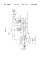
- FIGS. 1-3 are block diagrams of pipelined computer graphics systems employing the bus architecture of the invention
- FIG. 4 is a block diagram showing a generic embodiment of the bus architecture of the invention.
- FIG. 5 is a timing diagram showing the phases of operation of the system clock used in the invention.
- FIG. 6 is a more detailed block diagram of one of the interface circuits shown in FIG. 4;
- FIG. 7 is a timing diagram showing how address and data information may be clocked into various registers employed in the interface circuit shown in FIG. 6;
- FIG. 8 is a timing diagram showing the delay between when an interface circuit de-asserts its Buffered -- Ready signal to an upstream processing element and when the upstream processing element stops sending data to the interface circuit;
- FIG. 9 is a timing diagram showing the delay between when an interface circuit re-asserts its Buffered -- Ready signal to an upstream processing element and when the upstream processing element begins sending valid data to the interface circuit;
- FIG. 10 is a more detailed block diagram of the buffered and unbuffered write FIFOs shown in FIG. 6;
- FIG. 11 is a timing diagram showing the relationship between various signals used to control the buffered and unbuffered write FIFOs shown in FIG. 10;
- FIG. 12 is a more detailed block diagram of the buffered and unbuffered read FIFOs shown in FIG. 6 and shows how these FIFOs might operate when a processing element is configured in detour mode;
- FIG. 13 is a more detailed block diagram of the buffered and unbuffered read FIFOs shown in FIG. 6 and shows how these FIFOs might operate when a processing element is not configured in detour mode;
- FIG. 14 is a timing diagram showing the relationship between various signals used to control the buffered and unbuffered read FIFOs shown in FIGS. 12 and 13.
- FIGS. 1-3 are block diagrams showing different exemplary embodiments of computer graphics systems that employ a busing architecture and data transfer protocol according to the present invention. Each system has a different number of components and, therefore, offers a different level of performance; two of the systems shown also offer an additional texture mapping feature. It should be understood that the systems shown are exemplary and in no way limiting and that any data transfer system could utilize the busing architecture and data transfer protocol of the invention.
- FIG. 1 shows the simplest system of the three.
- the system includes a host computer 100, a front end subsystem 102 and a frame buffer subsystem 104.
- Front end subsystem 102 receives primitives to be rendered from host computer 100 over bus 101.
- the primitives typically are specified by x, y, z coordinate data, R, G, B color data, and alpha blending data, for each of certain portions of the primitives, such as the triangle vertices.
- Data representing the primitives in three dimensions is provided by front end subsystem 102 to the frame buffer subsystem over bus 122, having segments 122A, 122B and 122C.
- Frame buffer subsystem 104 interpolates the rendering data received from front end subsystem 102 to compute the pixels on the display screen that will represent each primitive, and to determine resulting object R, G, B color values for each pixel.
- R, G, B color control signals for each pixel respectively are provided over R, G, B lines 123 to control the pixels of the display screen (not shown) to display a resulting image thereon.
- front end subsystem 102 includes a host interface 106 and a three-dimensional (3-D) geometry accelerator 110.
- host interface 106 receives the x, y, z coordinates and color primitive data along bus 101 from host computer 100. Such data is provided from host interface 106 to geometry accelerator 110 along bus 108.
- Geometry accelerator 110 performs conventional geometry accelerator functions resulting in rendering data for display. Such functions may include three-dimensional transformation, lighting, clipping, and perspective divide operations, as well as plane equation generating, done in floating point format.
- the rendering data is provided by geometry accelerator 110 along bus 112 to host interface 106, which re-formats the rendering data, performs a floating point to fixed point conversion, and provides such data along bus system 122 to frame buffer subsystem 104.
- frame buffer subsystem 104 includes two frame buffer controllers 114A and 114B, each having a respective synchronous graphics random access memory (SGRAM)116A and 116B, as well as a random access memory digital-to-analog converter (RAMDAC) 120.
- bus system 122 Connected to bus system 122 are both frame buffer controllers 114A and 114B and host interface 106.
- bus 122 includes three buses 122A, 122B and 122C, each identical to the other.
- the bus architecture 122 and associated data transfer protocol which will be discussed in more detail below, offer improved bandwidth over prior art architectures and protocols.
- each frame buffer controller 114A and 114B receives rendering data from host interface 106.
- Each frame buffer controller may control different, non-overlapping segments of the display screen.
- the frame buffer controllers may interpolate the primitive data to compute the screen display pixel coordinates that represent the primitive, and the corresponding object R, G, B color values for each pixel coordinate.
- the resulting image video data generated by frame buffer controllers 114A and 114B may be stored in the corresponding SGRAMs 116A and 116B.
- Video data may be retrieved from the SGRAM chips into the frame buffer controllers, re-formatted so that it can be handled by RAMDAC 120, and provided to the RAMDAC.
- RAMDAC 120 may convert the digital color data to analog R, G, B color control signals for each pixel, which are provided along R, G, B lines 123 to control a screen display (not shown).
- Host interface 106 also may communicate directly with RAMDAC 120 through video bus 124.
- the system preferably is a pipelined system such that frame buffer subsystem 104 may operate on a first primitive while front end subsystem 102 is operating on a subsequent (in time) primitive.
- the bus system of the present invention also may be employed in the graphics system shown in FIG. 2.
- the system shown in FIG. 2 is similar to the system shown in FIG. 1 except that: (1) two 3-D geometry accelerators 110A and 110B are included in the front end subsystem 102, (2) a texture mapping subsystem 130 is employed, and (3) each SGRAM memory 116A and 116B has been increased in capacity.
- the primitive data is allocated among the geometry accelerators in accordance with the data transfer protocol of the invention, described in more detail below.
- Texture mapping subsystem 130 may be any subsystem that carries out texture mapping operations and, in this exemplary embodiment, includes a texture mapping circuit 132 and associated local cache memory 134 which stores a limited amount of texture data.
- bus 122 includes portions 122A-122D.
- Texture mapping circuit 132 is connected to bus 122 between host interface 106 and frame buffer controller 114A. During operation, texture mapping circuit 132, like both frame buffer controller circuits 114A and 114B, receives primitive data on bus 122A. The data may include x, y, z object pixel coordinates, object R, G, B color values, and S, T texture map coordinates for at least one vertex, and the plane equation of the primitive (i.e., triangle). Texture mapping circuit 132 may interpolate the x, y pixel coordinates and the S, T texture coordinates to compute resultant texture data for each pixel.
- the texture data for each pixel may, at any one time, be stored in cache memory 134. If so, then the texture data is read from cache memory 134. If the texture data needed is not at that time present in cache memory 134, then, without requiring the flushing of the data rendering pipeline or a dedicated texture data path, the needed texture data is downloaded from the host computer in an efficient manner in accordance with the present invention, as will be described in greater detail below.
- the texture data for each pixel may be provided along texel bus 136 to each frame buffer controller 114A and 114B where it is combined, on a pixel-by-pixel basis, with object, R, G, B color values by each frame buffer controller.
- front end subsystem 102, frame buffer subsystem 104 and texture mapping subsystem 130 may be any presently known subsystems or later-developed subsystems. Additionally, each of such subsystems preferably is pipelined and operates on multiple primitives simultaneously. As such, while texture mapping subsystem 130 and frame buffer subsystem 104 operate on primitives previously provided by front end subsystem 102, front end subsystem 102 continues to operate on new primitives until the pipelines in such downstream subsystems become full.
- the bus architecture of the present invention is configured such that different types of graphics processing chips may be arranged interchangeably within the architecture. That is, each chip connected to the bus 122 could perform any graphics function such as texture mapping, frame buffer control, or other such functions.
- FIG. 3 is a block diagram showing a further embodiment of a graphics system that employs the bus architecture of the present invention.
- front end subsystem 102 includes three 3-D geometry accelerators 110A, 110B and 110C;
- frame buffer subsystem 104 includes four frame buffer controllers 114A-114D, each with an associated SGRAM memory 116A-116D, respectively;
- texture mapping subsystem 130 includes two texture mapping circuits 132 and 133, each with an associated cache memory 134 and 135, respectively.
- bus segments 122A-G of bus architecture 122 of the present invention Connected by bus segments 122A-G of bus architecture 122 of the present invention are host interface 106, each of texture mapping circuits 132 and 133, and each of the frame buffer controllers 114A-114D.
- Texel bus 137 is connected between texture mapping circuit 133 and each of frame buffer controllers 114C and 114D. Operation is similar to that described with reference to FIG. 2.
- Bus interconnect system 200 which may be used to interconnect a number of graphics chips (e.g., frame buffer controllers), includes a number of processing elements 202, 222 and 242.
- Processing element 202 is interfaced to an external host device (not shown), such as a central processing unit (CPU), via a peripheral component interconnect (PCI) bus 201.
- external host device not shown
- PCI peripheral component interconnect
- Each of processing elements 202, 222 and 242 preferably includes an application specific integrated circuit (ASIC) chip, the core of which may be configured as any type of graphics processing device such as a frame buffer controller, a texture mapping device, etc.
- ASIC application specific integrated circuit
- FIGS. 1-3 Examples of systems that could employ bus interconnect network 200 are illustrated in FIGS. 1-3.
- host interface 106 is coupled to the host computer 100 via bus 101, and host interface 106 is ring interconnected with frame buffer controllers 114A and 114B.
- processing element 202 could correspond to host interface 106 (FIG. 1)
- PCI bus 201 (FIG. 4)
- processing elements 222 and 242 (FIG. 4) could correspond, respectively, to frame buffer controllers 114A and 114B (FIG. 1).
- each of processing elements 202, 222 and 242 includes a core processor 204, 224 and 244, and an interface circuit 206, 226 and 246, respectively.
- the core processor of each processing element may be the same or different, while interface circuits 206, 226, and 246 (preferably) are identical.
- Coupled between each core processor 204, 224 and 244 and its associated interface 206, 226 and 246 are several asynchronous first-in-first-out buffers (FIFOs) 208, 210, 212, 214, 228, 230, 232, 234, 248, 250, 252 and 254.
- FIFOs first-in-first-out buffers
- asynchronous FIFOs provide buffered (i.e., non-priority) information paths and unbuffered (i.e., priority) information paths both from interface circuits 206, 226 and 246 to core processors 204, 224 and 244, respectively, and from core processors 204, 224 and 244 to interface circuits 206, 226 and 246, respectively.
- buffered (i.e., non-priority) information and unbuffered (i.e., priority) information and the processing of each type of information between buffered (i.e., non-priority) and unbuffered (i.e., priority) information paths, respectively, will be explained in more detail below.
- buffered (i.e., non-priority) information and unbuffered (i.e., priority) information paths will be explained in more detail below.
- two distinct types of information may be transmitted between processing elements using a shared bus.
- Each packet of information is identified (by setting particular bits in type field data transmitted concurrently therewith) as being either buffered (i.e., non-priority) or unbuffered (i.e., priority) information.
- information identified as being buffered is transferred to a storage element that receives only buffered information (i.e., a non-priority information storage element) and information identified as being unbuffered is transferred to a storage element that receives only unbuffered information (i.e., a priority information storage element).
- unbuffered (i.e., priority) information always takes precedence over buffered (i.e., non-priority) information, but so that non-priority information is held in an information path that is separate from the unbuffered (i.e., priority) information path until the unbuffered (i.e., priority) information is through being processed
- significant advantages are provided over systems in which a pipeline path must be "flushed" before priority information may be forwarded through it.
- priority information is identified herein as being “unbuffered,” it nevertheless is processed through information storage elements, and as such, it really is “buffered” in the common sense of the word. Nevertheless, priority information is referred to herein as being unbuffered, since, with respect to the non-priority information, it is, in a sense, unbuffered.
- buffered write (BW) FIFO 228 i.e., a non-priority interface output storage element
- BW buffered write
- core processor 224 i.e., a non-priority interface output storage element
- UW unbuffered write
- FIFO 230 i.e., a priority interface output storage element
- buffered read (BR) FIFO 232 i.e., a non-priority interface input storage element
- buffered (BR) FIFO 232 i.e., a non-priority interface input storage element
- UR unbuffered read
- FIFO 234 i.e., a priority interface input storage element
- Processing elements 202, 222 and 242 are interconnected by a unidirectional bus including bus segments 250, 252 and 254.
- Bus segments 250, 252 and 254 of interconnect network 200 are identical in construction and width.
- bus segments 250, 252 and 254 interconnect processing elements 202, 222 and 242 in a ring format, with bus segment 250 interconnecting processing elements 202 and 222, bus segment 252 interconnecting processing elements 222 and 242, and bus segment 254 interconnecting processing elements 242 and 202.
- information from processing element 202 is forwarded to processing element 222
- information from processing element 222 is forwarded to processing element 242
- information from processing element 242 is returned to processing element 202.
- information may be exchanged between the external host device and processing element 202 (via PCI bus 201), and information may be circulated unidirectionally from each of processing elements 202, 222 and 242 to the processing element that follows it in the ring.
- This circular arrangement provides simple point-to-point connections between each adjacent pair of processing elements such that the output of each interface is required to drive the input of only the one interface that follows it in the ring. Because each processing element drives only one load, signal integrity problems are minimized and, as a result, a high bus bandwidth may be attained.
- the information that is transferred from element to element is transferred along with a clock signal.
- the need to provide system-wide clock synchronization is eliminated, and the addition of extra processing elements is achieved by merely plugging a new processing element into the ring. That is, this transferring of the clock with the information permits the number of elements included in the bus to be virtually without limit, although the integrity of the clock signal will, of course, degrade as the number of processing elements in the ring is increased.
- the ring interconnect system allows for an increase in communication bandwidth with a bus having a decreased width.
- High throughput is achieved by quickly forwarding information through interfaces of the ring, while allowing the core processors of each element to process commands asynchronously from the information transfer rate. Routing and signal integrity problems are reduced because the bus width is reduced and because there is only one load per bus.
- additional processing elements may easily be added to or deleted from the ring network without adverse effects on the synchronization of the system. Because of the small amount of time that each of the processing elements requires to extract information from the bus, the addition of extra processing elements into the ring adds only one extra clock cycle per added processing element, thus incurring minimal additional delay.
- a complete packet of information includes two distinct portions, with each portion comprising thirty-two bits of information.
- the two portions of each information packet are multiplexed in time so that, for each complete packet that is transferred, sixty-four bits of information actually are transferred between processing elements.
- a first portion of an information packet might include a thirty-two bit address
- a second portion of the packet (immediately following the first portion) might include a thirty-two bit data word.
- each portion of each complete information packet has a nine bit type data field associated with it, and this nine bit type field is transmitted concurrently with the information packet with which it is associated.
- bus segments 250, 252 and 254 has forty-one bus lines dedicated to the transfer of information and type data.
- bus lines 250F which includes thirty-two distinct bus lines, is dedicated to the unidirectional transfer of thirty-two bits of information between interface circuit 206 and interface circuit 226, and bus lines 250E, which includes nine distinct bus lines, is dedicated to the unidirectional transfer of nine bits of type data between interface circuit 206 and interface circuit 226.
- bus lines 250E and 250F together, are able to transfer nine bits of type data and thirty-two bits of information between processing elements 202 and 222.
- half-packets of information and type data are transferred at a rate of at least 200 MHZ.
- each of bus segments 250, 252 and 254 provides common signals between the processing elements that it interconnects.
- these signals include a clock signal (CLK) transmitted along bus line 250A, a buffered information ready signal (B -- Rdy) transmitted along bus line 250B, an unbuffered information ready signal (U -- Rdy) transmitted along bus line 250C, a busy signal (Busy) transmitted along bus line 250D, type field signals (Type 8:0! transmitted along bus lines 250E, and information field signals (Info 31:0! transmitted along bus lines 250F.
- CLK clock signal
- B -- Rdy buffered information ready signal
- U -- Rdy unbuffered information ready signal
- Busy busy signal
- Type 8:0! transmitted along bus lines 250E
- Info 31:0! transmitted along bus lines 250F.
- the clock signals (CLK), type field signals (Type 8:0!), and information field signals (Info 31:0!) are forwarded in a first, downstream direction from one processing element (such as processing element 202) to the next processing element (such as processing element 222) in the ring.
- the buffered information ready signals (B -- Rdy) and unbuffered information ready signals (U -- Rdy), as well as the busy signals (Busy) are provided in a reverse, upstream direction from a second processing element (such as processing element 222) to a first processing element (such as processing element 202) in the ring.
- Two of these "reverse-direction" signals, i.e., the B -- Rdy and U -- Rdy are used to control the flow of information between the processing elements, as will be described in more detail below.
- the busy signal is used to indicated whether or not any of the chips on the bus are busy.
- a register in the master processing element which may be read by the host, keeps track of whether or not any of the chips are busy. In this manner, the host can determine when it is able to perform certain operations involving the processing elements.
- bus interconnect system 200 can interconnect any number of processing elements without a significant degradation in signal integrity or bandwidth, since, as noted above, the clock is transmitted with the data and only one load is coupled to each source.
- bus architecture of the invention permits the addition of optional processing elements to perform functions such as texture mapping, image processing, volume rendering, or the addition of standard processing elements such as rasterizers or frame buffer controllers for increased performance and functionality.
- Another advantage provided by the bus structure is that by multiplexing (in time) two distinct, thirty-two bit information words, the number of pins required to exchange this information between the processing elements is one-half the number that would be required if the information packets were not so multiplexed.
- the speed of the bus i.e., 200 MHZ, is high enough that the multiplexing of thirty-two bits of address and thirty bits of data in the manner described above may be performed while still allowing the graphics device to meet performance goals. Since pin reduction is generally a major factor in ASIC design, the ability of the bus structure to meet performance goals with one-half the number of pins dedicated to information transfer provides a significant advantage over systems that use larger numbers of pins to transmit the same amount of information.
- bus architecture 200 may run at increased frequencies.
- bus segments 250, 252, and 254 are unidirectional. Unidirectional buses generally provide a faster data transfer rate than bidirectional busses, since there is no delay period associated with reversing the direction of the bus. Further, because there is no need to provide for and control both a transmit and a receive path, unidirectional bus structures typically are easier to manage and require less hardware.
- each of the processing elements of FIG. 4 includes a core processor (e.g., core processor 224), a number of write and read FIFOs (e.g., FIFOs 228, 230, 232 and 234), and an interface circuit (e.g., interface circuit 226), and, as also mentioned above, the core processor of each processing element need not be the same.
- core processor 204 of processing element 202 includes logic for interfacing with the host PCI bus, which need not be included in the other core processors.
- processing element 202 is the master processing element in ring network 200, and thus, as mentioned previously, it could correspond to host interface 106 in FIG. 1-3.
- processing element 202 processes input packets in a slightly different manner than the other processing elements coupled in the ring.
- a primary clock is divided into two phases, Phase 1 (P1) and Phase 2 (P2).
- packets that are communicated across the information lines may be, for example, multiplexed address/data information, with each packet (in one exemplary embodiment) comprising thirty-two bits of address information and thirty-two bits of data information (for a total of sixty-four bits of information per packet).
- Phase 1 (P1) an address portion of a packet may be transmitted over the information lines (e.g., bus lines 250F), and during Phase 2 (P2) the associated data portion of the packet may be transmitted over the information lines.
- a packet of information need not comprise an address packet followed by a data packet, and may include any combination of address and data information.
- an information packet may comprise a data packet followed by another data packet when an operation such as a block transfer is performed.
- a packet of information need not be multiplexed into two or more separate portions, and may alternatively be transmitted as a single multi-bit packet without departing from the intended scope of the invention.
- Each packet of information is received by an interface circuit (e.g., interface circuit 226) via a set of information lines (e.g., bus lines 250F). All packets received by a processing element are forwarded to the core processor of that processing element (e.g., core processor 224 of processing element 222) for handling.
- Each processing element has a unique base address associated with it so that, for example, during a read operation, five bits of an incoming address may be compared with the base address of the processing element to see whether the packet is intended for that processing element.
- all identical types of processing elements will share a common base address. If a particular packet does not concern a processing element, the core processor simply will drop the packet. Otherwise, the core processor will perform whatever function is dictated by the packet.
- the core processor e.g., core processor 224 will forward information read from its memory (after a slight delay) out to the interface circuit associated with it (e.g., interface circuit 226) so that the interface circuit can forward the information to the downstream processing elements (e.g., processing element 242).
- bus interconnect system 200 is able to operate at a high frequency is because each interface circuit, for each processing element (other than master processing element 202), holds information for only a minimal amount of time before passing it to the next processing element in the ring. That is, as information is transferred into each of processing elements 222 and 242, each of interface circuits 226 and 246, respectively, retrieves the information in an input register (not shown) during a first clock-cycle and forwards it to an output register (not shown) during a second clock cycle following the first clock cycle, which may be but is not necessarily the next succeeding clock-cycle. Thus, in one embodiment, there is only a one clock cycle latency incurred at each of processing elements 226 and 246. Thus, all packets received by a processing element (other than master processing element 202) are forwarded by its interface circuit to the next processing element in the ring.
- the master processing element because it is the start and the end of the ring interconnect, is configured to act in "detour mode."
- interface circuit 206 operates as two distinct halves. An input half (including write FIFOs 208 and 210) receives all of the address/data information from the ring and detours the received information through core processor 204, and an output half (including read FIFOs 212 and 214) receives new address/data information from core processor 204 and forwards this information to the next processing element in the ring.
- An input half including write FIFOs 208 and 210) receives all of the address/data information from the ring and detours the received information through core processor 204
- an output half including read FIFOs 212 and 214) receives new address/data information from core processor 204 and forwards this information to the next processing element in the ring.
- interface circuit 206 in master processing element 202 enters core element 204, and information is never passed directly from the input of interface 206 to the output thereof, as is done in each of interface circuits 226 and 246.
- the output half is able to receive commands from the host processor (via the PCI bus), pass on or modify such commands (or create additional commands in response thereto), and forward these commands to the ring.
- detour mode is described above as being used only for the master processing element, it is envisioned that it may be used for other processing elements in the ring as well to provide enhanced functionality.
- detour mode also may be used in other processing elements to permit those elements to perform functions such as image processing.
- image processing data generally is fed into a core processor, manipulated, and passed out of the core processor.
- the data received by a core processor typically is stored and processed in such a manner that the latency between the entry and the exit of the data can be very long.
- a different amount of data may enter the core than the amount of data that exits it.
- image processing may be handled by those processing elements without degrading the overall performance of the ring.
- Detour mode may also be used, for example, to allow a processing element to transmit a digital video stream to a video data processing element that is downstream from the transmitting processing element.
- the processing element(s) supplying the digital video stream always should be upstream from the video data processing element(s) receiving the digital video stream.
- the host places the digital video data processing element into detour mode by writing to a detour state hardware register (not shown) in the interface of the digital video processing element. No other operations should be performed on the interconnect after placing the video processing element in detour mode.
- the video processing element After being placed in detour mode, the video processing element then can generate writes to memory and overlay buffers, image buffers or texture caches in any of the downstream processing elements in the ring bus.
- Detour mode is enabled by setting a detour state hardware flag at each "to-be-detoured" interface circuit.
- the detour state hardware flag of interface circuit 206 is set permanently, while the detour state hardware flags of interface circuits 226 and 246 optionally may be set.
- master processing element 202 (in FIG. 4) initiates information packet communication in the ring network, it also provides the primary clock that is forwarded with the information. That is, in addition to master processing element 202 being configured to act in detour mode, it also is configured to act in "master mode.” All processing elements, regardless of whether or not they are configured to act in master mode, receive an incoming clock (In -- CLK) from an upstream processing element along with information from that processing element. This incoming clock In -- CLK is used to clock the input circuitry of the interface circuits (described below). Processing elements other the processing element 202, which are not configured to act in master mode, also use the incoming clock In -- CLK to clock the output circuitry of the interface circuit (described below).
- In -- CLK incoming clock
- interface circuit 206 is controlled such that its output circuitry is clocked using a source clock (Src -- CLK) generated by core processor 204, rather than the incoming clock (In -- CLK).
- the source clock Src -- CLK from the core of a "mastered" processing element therefore is forwarded along with the information from the core of that processing element to the next processing element in the ring.
- the manner in which either the source clock or the incoming clock is selected to provide timing to the output circuitry of an interface circuit (depending on whether or not it is configured to act in master mode), as well as the generation of appropriate timing signals therefrom, is described in more detail below.
- non-master processing elements e.g., processing elements 222 and 242
- the forwarding of information from one processing element to another in the ring is controlled largely by the interface circuit of the processing element (e.g., interface circuits 226 and 246).
- core processor 224 receives information via asynchronous buffered write (BW) and unbuffered write (UW) FIFOs 228 and 230, and passes information read from core processor 224 to the output of interface circuit 226 via asynchronous buffered read (BR) and unbuffered read (UR) FIFOs 232 and 234.
- BW buffered write
- UW unbuffered write
- FIFOs 228, 230, 232 and 234 are referred to as "asynchronous" because buffered write (BW) and unbuffered write (UW) FIFOs 228 and 230 receive information from interface circuit 226, and buffered read (BR) and unbuffered read (UR) FIFOs 232 and 234 transmit information to interface circuit 226 using a first clock (provided by interface circuit 226), while buffered write (BW) and unbuffered write (UW) FIFOs 228 and 230 transmit information to core processor 224, and buffered read (BR) and unbuffered read (UR) FIFOs 232 and 234 receive information from core processor 224 using a second clock (provided by core processor 224) that may have a different frequency than the first clock.
- asynchronous FIFOs 228, 230, 232 and 234 facilitates the transferring of information between the two devices.
- each of FIFOs 228, 230, 232 and 234 is capable of storing eighty-two bits (in parallel) per FIFO entry.
- buffered FIFOs i.e., non-priority interface storage elements
- unbuffered FIFOs i.e., priority interface storage elements
- each buffer entry of buffered write (BW) and unbuffered write (UW) FIFOs 228 and 230 correspond to the thirty-two information bits and nine type bits received during Phase 1 (P1) of the packet transmission, and the other forty-one of the bits correspond to the thirty-two information bits and nine type bits received during Phase 2 (P2) of the packet transmission.
- P1 Phase 1
- P2 Phase 2
- each buffer entry will include a thirty-two bit address, a nine-bit type field associated with the address, thirty-two bits of data, and a nine-bit type field associated with the data (which generally is a duplicate of the type field associated with the address).
- each of buffered write (BW) and unbuffered write (UW) FIFOs 228 and 230 should be at least five entries deep, and each of the read FIFOs should be at least one entry deep. However, it should be understood that the number of entries in each FIFO may be adjusted as required by the core.
- the clock signal forwarded between each processing element is a 200 MHZ clock.
- Each interface circuit e.g., interface circuit 226)
- uses a two-phase clocking system each phase of which operates at one-half the external clock frequency, i.e., each phase operates at 100 MHZ in this embodiment.
- FIG. 5 a timing diagram is shown that illustrates the relationship between the incoming system clock In -- CLK (from an upstream processing element) and two clocking phases phase 1 (P1) and phase 2 (P2) that are created internal to each of the interface circuits.
- the phase of operation i.e., P1 or P2
- only a single-phase clock will be described hereinafter.
- a processing element when a processing element is not configured to act in master mode, it will transmit the incoming clock In -- CLK as its outgoing clock (Out -- CLK), which is transmitted with outgoing information.
- Out -- CLK the outgoing clock
- the internally created phases P1 and P2 for the outgoing clock Out -- CLK will be identical to the internally created phases P1 and P2 for the incoming In -- CLK.
- a processing element when configured to act in master mode, however, it will use a source clock Src -- CLK from its core, rather than the incoming clock In -- CLK, to transmit data.
- an interface circuit when in master mode, will transmit a source clock as its outgoing clock Out -- CLK, and, to control the flow of outgoing information, will generate a two-phase clocking system (also including phases P1 and P2) that is similar to (but not identical to) that shown in FIG. 5.
- interface circuit 226 a detailed block diagram of interface circuit 226 is shown. Since, in one embodiment, the interface circuits of all of the processing elements in the ring are identical, the following description of interface circuit 226 should be understood as applying to each of interface circuits 206 and 246 as well. As noted previously, however, interface circuit 206 generally only operates in “detour mode” and “master mode,” so its operation will differ slightly from that of interface circuits 226 and 246.
- type data and multiplexed packets of information are provided concurrently to the input of interface circuit 226 and are latched into an input register 260 (i.e., an input storage element).
- Input register 260 may be included in the input pads of interface circuit 226, or may alternatively be located external to the interface circuit.
- the logic in interface circuit 226 is clocked using a two-phase clocking system.
- the incoming clock In -- CLK is provided to the input of a divide-by-two circuit 295, which provides output signals write clock (Wr -- CLK) and phase 2 clock (P2 -- CLK), which is the inverse of the Wr -- CLK signal and, thus, is high during phase P2.
- the signals Wr -- CLK and P2 -- CLK are used to control various registers in the interface logic, as described below.
- the incoming clock In -- CLK also is provided to one input of multiplexer 299.
- Multiplexer 299 also receives a source clock Src -- CLK from core processor 224 as a second input.
- multiplexer 299 will select the source clock Src -- CLK as its output, and will provide the source clock Src -- CLK as the output clock Out -- CLK to the output of interface circuit 226.
- multiplexer 299 will select the input clock In -- CLK as its output, and will provide the input clock In -- CLK as the output clock Out -- CLK.
- the output of multiplexer 299 also is provided to the input of a divide-by-two circuit 297, which provides a read clock RD -- CLK, as well as a signal (not shown) that is the inverse of RD -- CLK and is used for output control, at its output.
- a divide-by-two circuit 297 which provides a read clock RD -- CLK, as well as a signal (not shown) that is the inverse of RD -- CLK and is used for output control, at its output.
- write clock Wr -- CLK and read clock RD -- CLK should be synchronous, and both should be the inverse of P2 -- CLK.
- the read clock RD -- CLK will be driven solely by the source clock Src -- CLK.
- the clocks created by divide-by-two circuits 295 and 297 may be synchronized system-wide by toggling the state of a single bit of information on one of the information bus lines, e.g., Bit 31! of bus lines 250F (shown in FIG. 4), and synchronizing the outputs of divide-by-two circuits 295 and 297 thereto.
- interface circuit 226 is able to quickly forward information packets (and type data) through its circuitry into output register 300 for transmission to the next processing element.
- Pass through path 261 is used whenever backup path 290 (described below) is empty and the downstream processing element (not shown) provides a signal to interface circuit 226 indicating that it presently is capable of receiving information. However, if the downstream processing element indicates that it is not able to receive information, the information that would have been passed to the downstream element (had it been ready to receive the information) is stored in information storage elements (e.g., registers) within a backup information path 290 (described below).
- This backed up information must be stored in information storage elements of backup information path 290 at least until interface circuit 226 stops receiving information from an upstream processing element (e.g., processing element 202 in FIG. 4).
- the upstream processing element will stop transmitting this information in response to interface circuit 226 providing a signal to the upstream processing element instructing it to halt its transmission of information.
- information packets transferred between processing elements comprise two portions.
- the first portion may comprise address information and the second portion may comprise data associated with that address.
- a type field associated with each of the two portions of an information packet.
- the type field includes nine bits, and may be encoded as shown below in Table I:
- the type field is used to provide instruction to each of the processing elements regarding what to do with the information it receives concurrently therewith.
- Two type fields that are commonly used are the Register Read and Register Write type fields.
- a Register Write is performed in two steps. First the address is sent over the bus during Phase 1 (P1) and, second, data is sent during Phase 2 (P2). For Register Reads, the address is sent during Phase 1 (P1), and the data field, sent during Phase 2 (P2), is unknown. After a brief delay, the data read from the core processor is inserted into the previously unknown data slot of the same register read packet and is forwarded to the next processing element in the ring.
- BIN Read and BIN Write instructions Two other commonly used type fields are BIN Read and BIN Write instructions, which are for reading and writing BIN type data (i.e., reading and writing information to specific buffers such as overlay buffers, image buffers or texture caches).
- Block Transfer instructions may be used to transfer large blocks of data between a source and a destination. For example, a large block of data could be transferred from the host computer (via the master processing element) to a downstream processing element by using Direct Memory Access (DMA) techniques.
- Plane Equation instructions may be included in the type field to transfer plane equation data to registers for 3D rendering.
- Miscellaneous (Misc) type instructions are used to implement special functions on the bus.
- the Misc type instruction could be used to flush a read path prior to performing any other type of operation.
- some instructions share bits with common meanings. For example, Bit ⁇ 8> of the type field is a "Valid" bit, which is used to indicate the validity of each of the portions of an information packet. If the Valid bit is a ⁇ 0 ⁇ , bits ⁇ 7:0>of the type field are ignored.
- Bit ⁇ 3> of the type field typically is used to identify whether a buffered (i.e., non-priority) information path or an unbuffered (i.e., priority) information path should be used to: (1) transfer information from the interface circuit to the core processor, (2) transfer information from the core processor to the interface circuit, or (3) hold information in the backup information path (described above). More details on buffered and unbuffered information paths will be provided below.
- interface circuit 226 includes an input register 260, a P1 register 262, a P1WD register 264 and a P2WD register 266.
- Input register 260 receives incoming information packets (and their associated type data), and P1 register 262 receives its input from the output of input register 260. Additionally, P1WD register 264 receives its input from the output of P1 register 262, and P2WD register receives its input from the output of input register 260.
- FIG. 7 a timing diagram is shown that illustrates the receipt of several complete information packets by interface circuit 226.
- this timing diagram illustrates: (1) the state of the incoming clock (In -- CLK) received on bus line 250A, (2) the information (Info 31:0! received on bus lines 250F, (3) the write clock signal (Wr -- CLK) output from divide-by-two circuit 295, and (4) the contents of input register 260 (IN -- Reg), P1 Register 262 (P1 -- Reg), and P1WD and P2WD registers 264 and 266, respectively (P1/P2WD).
- IN -- Reg input register 260
- P1 Register 262 P1 -- Reg
- P1WD and P2WD registers 264 and 266, respectively P1/P2WD
- the control of the "next-state" contents of each of the individual information storage elements shown in FIG. 6 may be implemented by using a software simulation language such as Verilog, and then converted into a logic gate circuit by a synthesis tool such as SynopsysTM operating on a general purpose processor.
- the logical functions alternatively may be written in software and performed by a processor.
- an output register of an upstream processing element forwards, for example, address ADDR1 (i.e., an address portion of a first information packet) over the bus lines 250F.
- address ADDR1 i.e., an address portion of a first information packet
- the falling edge of incoming clock In -- CLK latches ADDR1 into input register 260 of interface circuit 226.
- the falling edge of incoming clock In -- CLK latches the data portion DATA1 of the first information packet into input register 260.
- Type data is received by interface circuit 226 (from bus lines 250E) in an identical manner.
- information and type data is received by interface circuit 226 at the frequency of the incoming clock In -- CLK, i.e., at approximately 200 MHZ.
- phase P1 register 262 is provided. As the information (and associated type fields) are received by interface circuit 226 as described above, P1 register 262 is controlled by one-half frequency clock Wr -- CLK so as to latch only the first portion of each information packet. Also, P1/P2WD registers 264/266 (for forwarding information to core processor 224) are controlled by one-half frequency clock P2 -- CLK (which is the inverse of one-half frequency clock Wr -- CLK) so as to simultaneously latch both portions of each information packet.
- the contents of input register 260 is latched into P1 register 262 and, during the rising edge of one-half frequency clock P2 -- CLK (which is falling edge of Wr -- CLK), the contents of P1 register 262 is latched into P1WD register 264 and the contents of input register 260 is latched into P2WD register 266.
- P1/P2WD registers 264 and 266 store, respectively, the first portion and second portion of an information packet.
- the information in the P1/P2WD registers is loaded into either the buffered (i.e., non-priority) asynchronous write (BW) FIFO 228 or the unbuffered (i.e., priority) asynchronous write (UW) FIFO 230, depending on the values of certain bits in the type fields associated with the packet, as will be explained in more detail below.
- BW buffered
- UW unbuffered
- UW asynchronous write
- all incoming multiplexed packets of information is received by input register 260 on each falling edge of the incoming clock In -- CLK (as noted above), and information from either: (1) input register 260 (via pass through path 261), (2) backup information path 290, or (3) buffered read (BR) or unbuffered read (UR) FIFOs 232 or 234, is clocked into output register 300 (via one or more of multiplexers 270, 282 and 280) on the falling edges of output clock Out -- CLK (which is the same as input clock In -- CLK when processing element is not in master configuration) as well.
- BR buffered read
- UR unbuffered read
- input register 260 and output register 300 receive and transmit information on each falling edge of input clock In -- CLK, i.e., during both the P1 and P2 transfer cycles. Because information packets are multiplexed into two portions (e.g., an address portion and a data portion), input register 260 actually receives the first portion of each information packet, e.g., the address information, on the falling edge of input clock In -- CLK during a P2 phase of operation, and receives the second portion of the information packet, e.g., the data information, on the falling edge of input clock In -- CLK during a P1 phase of operation (that immediately follows the P2 phase during which the address was clocked into register 260).
- first portion of each information packet e.g., the address information
- the second portion of the information packet e.g., the data information
- each information packet that is transmitted by interface circuit 226 is clocked into output register 300 by a falling edge of output clock Out -- CLK (which is the same as input clock In CLK when processing element is not in master configuration) during a P1 phase of operation
- the second portion of each transmitted information packet is clocked into output register 300 by a falling edge of output clock Out -- CLK during a phase P2 of operation (that immediately follows the P1 phase during which first portion of the packet was clocked into register 300).
- output register 300 will receive information directly from input register 260 (via pass through path 261) so that one portion of an information packet (and its associated type data) is shifted through interface circuit 226 during each falling edge of input clock In -- CLK and a latency of only a single clock cycle is incurred as a result of the presence of the interface circuit.
- processing element downstream from processing element 222 indicates that it presently is not capable of receiving information from processing element 222, or if processing element 222 is itself stalled (e.g., when waiting for read information from its core)
- information storage elements within backup information path 290 are used to store information that gets backed up in interface circuit 226 while the processing element that is upstream from processing element 222 (e.g., processing element 202) is still sending data, i.e., until upstream processing element 202 responds to an indication from processing element 222 that it currently is unable to accept information. That is, this backup function is performed at least until interface circuit 226 is able to signal to the upstream processing element (e.g., processing element 202) to stop sending information.
- backup information path 290 includes a buffered (i.e., non-priority) information backup path 292 and an unbuffered (i.e., priority) information backup path 294.
- Buffered information backup path 292 includes buffered (i.e., non-priority) backup storage elements B0, B1, B2, B3, B4 and B5, and unbuffered information backup path 294 includes unbuffered (i.e., priority) backup storage elements U0, U1, U2, U3, U4 and U5.
- multiplexers 292A and 292B are arranged to selectively provide the contents of only one (or none) of buffered backup storage elements B4 and B5 and unbuffered backup storage elements U4 and U5 to one of the inputs of multiplexer 270 to which the outputs of multiplexers 292A and 292B are connected.
- B -- Rdy register 322 receives an incoming buffered ready (B -- Rdy -- In) signal from a downstream processing element (via B -- Rdy logic circuit 326), and provides an outgoing buffered ready (B -- Rdy -- Out) signal to an upstream processing element.
- B -- Rdy register 322 receives an incoming buffered ready (B -- Rdy -- In) signal from a downstream processing element (via B -- Rdy logic circuit 326), and provides an outgoing buffered ready (B -- Rdy -- Out) signal to an upstream processing element.
- U -- Rdy register 324 receives an incoming unbuffered ready (U -- Rdy -- In) signal from a downstream processing element (via U -- Rdy logic circuit 328), and provides an outgoing unbuffered ready (U -- Rdy -- Out) signal to an upstream processing element.
- B -- Rdy and U -- Rdy logic circuits 326 and 328 receive a number of other inputs in addition to the incoming B -- Rdy -- In and U -- Rdy n signals, any of which may indicate the present inability of processing element 222 to receive information from an upstream processing element.
- Each of B -- Rdy and U -- Rdy registers 322 and 324 is clocked on the rising edge of the Wr -- CLK signal.
- Downstream processing elements signal upstream processing elements to halt information transmission simply by de-asserting their outgoing buffered ready (B -- Rdy -- Out) signals (e.g., on bus line 250B) or their outgoing unbuffered ready U -- Rdy -- Out) signals (e.g., on bus line 250C) to the upstream element.
- B -- Rdy -- Out and U -- Rdy -- Out signals indicate the relative ability of processing element 222 to receive buffered (i.e., non-priority) information and unbuffered (i.e., priority) information. More explanation regarding the use and control of buffered and unbuffered information will be provided in detail below.
- Backup information path 290 in FIG. 6 includes three stages of buffering in each of its buffered and unbuffered information paths 292 and 294 to accommodate the maximum amount of information that might be backed up, for example, between the time that interface circuit 226 first receives an incoming de-asserted B -- Rdy -- In signal from downstream interface circuit 246 and the time that interface circuit 226 actually stops receiving information from upstream interface circuit 206 (after interface circuit 226 has de-asserted its outgoing buffered ready signal B -- Rdy -- Out to upstream interface circuit 206).
- interface circuit 226 The receipt of either the incoming B -- Rdy -- In or the U -- Rdy -- In signal by interface circuit 226 (from a downstream processing element) will cause interface circuit 226 to halt transmission of information of the identified type (i.e., either buffered or unbuffered information) to the downstream processing element and to store any pending information, as well as any information received during the time between when interface circuit 226 de-asserts its outgoing B -- Rdy -- Out or U -- Rdy -- Out signal (to an upstream processing element) and the time when the upstream processing element actually stops sending information of the identified type, into dedicated buffers included backup information path 290.
- information of the identified type i.e., either buffered or unbuffered information
- the receipt of a de-asserted incoming B -- Rdy -- In or U -- Rdy -- In signal is an indication that the processing element receiving the signal should stop sending information and type data (as soon as possible) on its outgoing information and type data bus lines.
- interface circuit 226 Once interface circuit 226 receives a de-asserted B -- Rdy -- In or U -- Rdy -- In signal from a downstream processing element, it will halt its information transfer only after it is through sending any complete packet of information that it already had started to send when it received the signal. Thus, for example, if interface circuit 226 receives a de-asserted B -- Rdy -- In signal from interface circuit 246 just after an address (associated with a non-priority operation) has been clocked into output register 300, interface circuit 226 will proceed to clock the data portion of the information packet (associated with the previously sent address) before halting information transfer to downstream processing element 246.
- backup path 290 also is latched into P1WD register 264 and P2WD register 266 and is transferred to either buffered write (BW) FIFO 228 or unbuffered write (UW) FIFO 230 (depending on whether the information is buffered or unbuffered), so that even the "backed up" information will reach core 224 (in case the information concerns the core).
- BW buffered write
- UW unbuffered write
- buffered backup path 292 are intended to represent inputs to each pair of buffered backup storage elements (i.e., B0 and B1, B2 and B3, and B4 and B5) in buffered backup path 292.
- buffered backup path 292 In contrast to how buffered backup path 292 is filled, when buffered backup path 292 is emptied, information (and type data) always is read from registers B4 and B5. Additionally, when registers B4 and B5 are emptied, the contents (if any) of registers B2 and B3 is shifted to registers B4 and B5, respectively, and the contents (if any) of registers B0 and B1 is shifted to registers B2 and B3, respectively.
- a number of separate, single-bit registers i.e., contents-identifying storage elements
- registers 302, 304, 306, 308, 310, 312 and 314 included in control register block 320 are utilized to keep track of what type of information is in which locations in backup information path 290, as well as what type of information is in P1 register 262.
- individual register 302 may be used to indicate whether buffered backup registers B4 and B5 are full
- individual register 304 may be used to indicate whether buffered backup registers B2 and B3 are full
- individual register 306 may be used to indicate whether buffered backup registers B0 and B1 are full
- individual register 308 may be used to indicate whether buffered backup register B0 has information of the miscellaneous type stored in it
- individual register 310 may be used to indicate whether buffered backup register B2 has information of the miscellaneous type stored in it
- individual register 312 may be used to indicate whether buffered backup register B4 has information of the miscellaneous type stored in it
- individual register 314 may be used to indicate whether P1 register 262 has buffered information of the miscellaneous type stored in it.
- Similar registers also are provided in control register block 320 to indicate whether each of backup registers B0, B2 and B4, as well as P1 register 262, has other specific kinds of information stored in it, such as an address that matches the base address of the core of that processing element, an address of BIN read packet, or a Block Transfer (BltOb) packet, as defined in table I above. Similar information also is stored in additional single-bit registers (not shown) in control register block 320 (i.e., contents-identifying storage elements) to identify the contents of the unbuffered (i.e., priority) backup storage elements, e.g., registers, included in unbuffered backup path 294.
- single-bit "type-identifying" registers (not shown) in control register block 320 are used to identify whether P1 register 262 contains certain types of buffered information, e.g., buffered BltOb information, than are used to identify whether it contains certain types of unbuffered information, e.g., unbuffered BltOb information.
- the B -- Rdy -- Out signal has two states; an asserted state, indicating that the processing element transmitting the B -- Rdy -- Out signal is available to accept information, and an un-asserted state, indicating that the processing element is unavailable to accept information.
- the asserted state corresponds to a logic ⁇ 1 ⁇ and the de-asserted state corresponds to a logic ⁇ 0 ⁇ .
- a processing element may be unable to accept information for a variety of other reasons.
- buffered write (BW) FIFO 228 i.e., a non-priority information storage element
- BW buffered write
- FIFO 228 i.e., a non-priority information storage element
- interface circuit 226 cannot receive much more information
- B -- Rdy logic circuit 326 will cause the outgoing B -- Rdy -- Out signal to be de-asserted (on the next Wr -- CLK) to halt the upstream processing element from transmitting information, thus insuring that input information does not get dropped.
- B -- Rdy logic circuit 326 will cause the outgoing B -- Rdy -- Out signal to be de-asserted (on the next Wr -- CLK) when an incoming information packet is encoded to perform a read operation from core 224.
- a read operation may include a read of one or more core registers, or a read of a memory device (such as a frame buffer) coupled to the core.
- processing element 222 When a read packet (e.g., a register read packet) is received when no pre-fetched data is present, processing element 222 is receiving an indication that it should stop sending information and type data (as soon as possible) to the downstream processing element. That is, a read packet being received by processing element 222 constitutes an indication that processing element 222 (in addition to signaling the upstream processing element to stop sending information) currently should stop sending information and type data (as soon as possible) to the downstream processing element insofar as processing element 222 must wait for information to be read from its core before that information (multiplexed with the previously received address) may be transmitted to the downstream processing element.
- a read packet e.g., a register read packet
- BR buffered read
- UR unbuffered read
- P1 -- OUT, P2 -- OUT, U -- P1 -- OUT and U -- P2 -- OUT 272, 274, 276 and 278, respectively.
- the address of the read is stored in an information storage element within backup information path 290 and processing element 224 de-asserts its outgoing B -- Rdy -- Out signal on bus line 250B to signal the upstream processing element to stop sending information.
- processing element 224 de-asserts its outgoing B -- Rdy -- Out signal on bus line 250B to signal the upstream processing element to stop sending information.
- the data is returned from core processor 224, it propagates through buffered read (BR) FIFO 232 and is stored in P2 -- OUT register 274.
- BR buffered read
- the B -- Rdy -- Out signal is re-asserted (indicating that the upstream processing element may again send information), the address corresponding to the read is forwarded through multiplexers 292A, 270 and 282, and is output on the rising edge of the next P2 -- CLK signal.
- the retrieved data (after propagating through multiplexers 280 and 282) then is output on the rising edge of the next RD -- CLK signal.
- the B -- Rdy -- Out signal may be used to temporarily halt upstream processing elements until read data is available. Resultingly, after the core read is performed, the address and the data retrieved from that address, may be transmitted synchronously with a delay period determined (essentially) only by the delay associated with the core read operation.
- FIG. 8 a timing diagram is provided that illustrates the time latency that is incurred between when the outgoing B -- Rdy -- Out signal is de-asserted by processing element 222 after it has received, for example, a core read packet, and when processing element 222 actually stops receiving information from an upstream processing element (e.g., processing element 202).
- processing element 222 actually stops receiving information from an upstream processing element (e.g., processing element 202).
- These signals are shown on the same time scale (horizontal axis) for comparison.
- the physical placement of one signal above another does not denote that one attains a higher magnitude than the other signals.
- phase 1 (P1) and phase 2 (P2) of each transfer cycle address and data information, respectively, are received on bus lines 250F. If the type information associated with an address sent during phase P1 of transfer cycle T1 indicates that a core read operation is to be performed, then during phase P2 of transfer cycle T1, the B -- Rdy -- Out signal is de-asserted. As is indicated by the high state of Bit ⁇ 8> of the type field (i.e., the Valid signal), valid address and data information continue to be received on the bus lines 250F until the end of transfer cycle T2. The time delay between when the B -- Rdy -- Out signal is de-asserted during transfer cycle T1, and when information stops being transmitted on the bus during transfer cycle T2 results in a backup of information at processing element 222.
- FIG. 9 a similar delay is illustrated between the time when the B -- Rdy -- Out signal is re-asserted by processing element 222 and the time when processing element 222 again receives valid information from an upstream processing element (e.g., processing element 202).
- These signals are shown on the same time scale (horizontal axis) for comparison. The physical placement of one signal above another does not denote that one attains a higher magnitude than the other signals.
- This time delay allows for information in backup information path 290 to be forwarded out of output register 300 before new information is received by input register 260 of interface circuit 226.
- a first portion of an incoming information packet (e.g., address and address type information) is received at the input of input register 260 during phase P1 of a transfer cycle.
- the first portion of the information packet is latched into input register 260.
- the information stored in input register 260 is loaded into P1 register 262 at the same time that a second portion of the information packet (e.g., data and data type information) is loaded into input register 260.
- Both portions of information then are forwarded to the first stage of buffered backup path 292 (i.e., registers B4 and B5) on the succeeding P2 clock phase.
- Information continues to be transferred from P1 register 262 and input register 260 into succeeding registers (i.e., buffered backup storage elements) in buffered backup path 292 (on succeeding P2 clock phases) until the upstream processor stops transmission in response to interface circuit 226 de-asserting its outgoing B -- Rdy -- Out signal.
- interface circuit 226 again is ready to receive and/or send information, its outgoing -- Rdy -- Out signal is asserted, and the process of emptying the registers in buffered backup path 292 begins.
- Phase 1 (P1) of the first transfer cycle after the outgoing B -- Rdy -- Out signal has been re-asserted information from register B4 is forwarded through multiplexers 292A, 270 and 282, and latched into output register 300.
- Phase 2 (P2) of the same transfer cycle information from register B5 is forwarded through multiplexers 292A, 270 and 282, and latched into output register 300.
- Phase 1 (P1) and Phase 2 (P2) of the second transfer cycle information from registers B4 and B5, respectively, which (if present) has been shifted from registers B2 and B3, is forwarded to output register 300.
- Phase 1 (P1) of the third transfer cycle information from register B4, which (if present) has been shifted from register B0 to register B2 during the first transfer cycle and from register B2 to register B4 during the second transfer cycle, is forwarded through the multiplexers to output register 300.
- an upstream processing element e.g., processing element 202
- Phase 2 (P2) of the third transfer cycle the first portion of the information packet from the upstream processing element is latched into input register 260 at the same time that information from register B5, which (if present) has been shifted from register B1 to register B3 during the first transfer cycle and from register B3 to register B5 during the second transfer cycle, is latched into output register 300, thereby emptying buffered backup path 292.
- Phase 1 (P1) of the fourth transfer cycle the second portion of the information packet from the upstream processing element can be latched into input register 260 at the same time that the first portion of the information packet (that was previously latched into input register 260) can be forwarded directly to output register 300 via pass-through path 261. Because buffered backup path 292 is sized so as to accommodate the maximum amount of information that possibly could be backed up therein, no information is lost when a processing element halts operation and high speed communication throughput is maintained.
- each incoming information packet (as well as its associated type field) are latched, respectively, into P1 register 262 and input register 260 (i.e., an input storage element) prior to being latched, respectively, into P2WD register 266 and P1 WD register 264, and forwarded to core processor 224 of processing element 222.
- P1 register 262 and input register 260 i.e., an input storage element
- Both portions of each information packet latched into P1WD and P2WD registers 264 and 266 are input into either buffered write (BW) FIFO 228 (i.e., a non-priority interface output storage element) or unbuffered write (UW) FIFO 230 (i.e., a priority interface output storage element), depending on the contents of the type field of the first portion of the packet. That is, the type field of the first portion of the packet, i.e., the portion stored in P1 register 262, is examined to determine whether the packet, according to the listings in Table I, is identified as being buffered or unbuffered.
- BW buffered write
- UW unbuffered write
- Bit ⁇ 7> of this type field is a "1”
- Bit ⁇ 7> is a "0
- whether the packet is transferred to buffered write (BW) FIFO 228 or unbuffered write (UW) FIFO 230 depends on the value of Bit ⁇ 3> of the type field.
- Bit ⁇ 3> of the type field of the first portion of a packet is a "1”
- the information is of the unbuffered type and, conversely, if Bit ⁇ 3> is a "0”
- the information is of the buffered type.
- two separate single-bit registers are employed to keep track of whether P1 register 262 currently contains buffered or unbuffered information.
- register 316 may be used to indicate whether P1 register 262 presently contains buffered information
- register 318 may be used to indicate whether P1 register 262 presently contains unbuffered information.
- next-state contents of each of registers 316 and 318 may be determined by examining the type field of the information stored in input register 260, so that P1 register 262 will receive input information and registers 316 and 318 will receive inputs corresponding to the type of information input to P1 register 262 during the same clock cycle.
- each of buffered write (BW) and unbuffered write (UW) FIFOs 228 and 230 includes eight entries to store each of the two portions of an information packet. That is, each of buffered write (BW) and unbuffered write (UW) FIFOs 228 and 230 includes eight entries to store: (1) phase 1 information and type data (P1 -- WrInfo and P1 -- WrType) from P1WD register 264, and (2) phase 2 information and type data (P2 13 WrInfo and P2 -- WrType) from P1WD register 266.
- FIFO 228 also includes a load control circuit 227 and an unload control circuit 229
- unbuffered write (UW) FIFO 230 also includes a load control circuit 231 and an unload control circuit 233.
- FIG. 11 a timing diagram is provided that shows the relationship between the incoming clock signal In -- CLK, the write clock signal Wr -- CLK from divide-by-two circuit 295 (shown FIG. 6 ), and the P1 and P2 -- WrInfo (which is the information that has been written to FIFO 228 or 230 from registers 264 and 266). These signals are shown on the same time scale (horizontal axis) for comparison. The physical placement of one signal above another does not denote that one attains a higher magnitude than the other signals. As shown in FIG. 10, each of load control circuits 227 and 231 receives the Wr -- CLK signal as a clock input.
- Load control circuit 227 also receives a buffered information load signal (B -- WrInfoLd), which is a result of the above-explained examination of the type bits to identify whether information is of the buffered or unbuffered type.
- Load control circuit 227 provides a buffered write full signal (B -- WrFull), which is asserted when buffered write (BW) FIFO 228 is within four entries of being full and is de-asserted when buffered write (BW) FIFO 228 has five or more entries available to be filled.
- load control circuit 231 receives an unbuffered information load signal (U -- WrInfoLd), which also is a result of the above-explained examination of the type bits to identify whether information is of the buffered or unbuffered type.
- Load control circuit 231 provides an unbuffered write full signal (U -- WrFull), which is asserted when unbuffered write (UW) FIFO 230 is within four entries of being full and is de-asserted when unbuffered write (UW) FIFO 230 has five or more entries available to be filled.
- Each of unload control circuits 229 and 233 also receives a respective core clock signal and an unload signal from the core (which permit the core to unload information from the FIFOs at the core clock rate when one of the unload signals is asserted), and provides a respective empty signal to the core (which indicates to the core that that FIFO presently has no information stored in it).
- the core may access the P1 and P2 information and type data (P1 -- Info, P1 -- Type, P2 -- Info and P2 -- Type) from either of buffered write (BW) and unbuffered write (UW) FIFOs 228 and 230, at a rate that is asynchronous to the clock rate at which these FIFOs receive the information and type data from interface circuit 226.
- BW buffered write
- UW unbuffered write
- FIGS. 12 and 13 shows asynchronous buffered read (BR) and unbuffered read (UR) FIFOs 232 and 234 in more detail.
- FIG. 12 shows how buffered read (BR) and unbuffered read (UR) FIFOs 232 and 234 might operate when processing element 222 is configured in detour mode
- FIG. 13 shows how buffered read (BR) and unbuffered read (UR) FIFOs 232 and 234 might operate when processing element is not configured in detour mode (such as the configuration shown in FIG. 6).
- a selected one of buffered read (BR) and unbuffered read (UR) FIFOs 232 and 234 receives both portions of an information packet (i.e., phase 1 information (P1 -- Info) and type data (P1 -- Type) and phase 2 information (P2 -- Info) and type data (P2 -- Type)) from the core, along with a core clock and a load signal, and provides to the core a "full" signal to indicate to the core when the respective one of the FIFOs is full.
- each of buffered read (BR) and unbuffered read (UR) FIFOs 232 and 234 is eight entries deep, but the necessary depth of the read FIFOs will be determined by the operations to be performed by the core.
- buffered read (BR) FIFO 232 provides both portions of a buffered information packet (i.e., phase 1 output information (P1 -- OutInfo) and type data (P1 -- OutType) and phase 2 output information (P2 -- OutInfo) and type data (P2 -- OutType) to interface circuit 226.
- phase 1 output information P1 -- OutInfo and type data P1 -- OutType is provided to P1 -- OUT register 272
- phase 2 output information P2 -- OutInfo and type data P2 -- OutType is provided to P2 -- OUT register 274.
- unbuffered read (UR) FIFO 234 provides both portions of an unbuffered information packet to interface circuit 226.
- phase 1 unbuffered output information (P1 -- U -- OutInfo) and type data (P1 -- U -- OutType) is provided from unbuffered read (UR) FIFO 234 to U -- P1 -- OUT register 276 and phase 2 unbuffered output information (P2 -- U -- OutInfo) and type data (P2 -- U -- OutType) is provided from unbuffered read (UR) FIFO 234 to U -- P2 -- OUT register 278.
- buffered read (BR) and unbuffered read (UR) FIFOs 232 and 234 receives information from the core along with mask data, explained below, associated with the information.
- BR buffered read
- UR unbuffered read
- buffered read (BR) FIFO 232 provides either of the two portions of a buffered information packet (i.e., either phase 1 buffered output information (P1 -- OutInto) or phase 2 buffered output information (P2 -- OutInfo)), as well as the mask data (OutMask) from the core, to interface circuit 226.
- phase 1 buffered output information P1 -- OutInfo or phase 2 buffered output information P2 -- OutInfo is provided to both of P1 -- OUT register 272 and P2 -- OUT register 274, and thirty-two bits of buffered mask data (OutMask) is provided to mask register 284.
- unbuffered read (UR) FIFO 234 provides either portion of an unbuffered information packet, as well as unbuffered mask data (OutMask) from the core, to interface circuit 226.
- phase 1 unbuffered output data (P1 -- U -- OutInfo) or phase 2 unbuffered output data (P2 U OutInfo) is provided to both of U -- P1 -- OUT register 276 and U -- P2 -- OUT register 278, and unbuffered mask data (OutMask) is provided to mask register 284.
- P1 -- U -- OutInfo phase 1 unbuffered output data
- P2 U OutInfo phase 2 unbuffered output data
- OutMask unbuffered mask data
- the buffered mask data (OutMask) transferred to mask register 284 (when buffered information is being read) is used to perform a selective masking or "bit slicing" of the buffered information output from the core.
- the thirty-two bit mask selects buffered information, on a bit-by-bit basis, from one of: (1) the buffered information output from the core, and (2) either the buffered information flowing through pass through path 261 or the buffered information read from backup information path 290.
- the single bit of unbuffered mask data (OutMask) transferred to mask register 284 (when unbuffered information is being read) is used to select an entire thirty-two bit information word from one of the two sources just listed. It should be noted that, alternatively, thirty-two bits of unbuffered mask data could be used to selectively mask "bit-by-bit" the unbuffered information from the core.
- FIG. 14 a timing diagram is provided that shows the relationship between the outgoing clock signal Out -- CLK, the read clock signal RD -- CLK from divide-by-two circuit 297 (shown in FIG. 6), and the buffered output information from one of read FIFOs 232 and 234.
- Buffered output information, i.e., P1 and P2 -- OutInfo, from buffered read (BR) FIFO 232 is shown as an example and could just as well represent unbuffered output information P1 and P2 -- U -- OutInfo.
- These signals are shown on the same time scale (horizontal axis) for comparison. The physical placement of one signal above another does not denote that one attains a higher magnitude than the other signals.
- buffered read (BR) FIFO 232 includes unload control circuit 235 and load control circuit 237
- unbuffered read (UR) FIFO 234 includes unload control circuit 239 and load control circuit 241.
- the information and mask data is loaded into one of the FIFOs upon a transition of the core clock when the load signal to one of load control circuits 237 or 241 is asserted, and is unloaded from one of the FIFOs upon a transition of the clock signal RD -- CLK when either the buffered or unbuffered unload signal (B -- OutInfoUnld or U -- OutInfoUnld) to one of unload control circuits 235 and 239 is asserted.
- the signals B -- OutDatVal and U -- OutDatVal from unload control circuits 235 and 239, respectively, indicate that buffered or unbuffered information is ready to be clocked into a corresponding one of read registers 272, 274, 276 and 278.
- FIFOs 228, 230, 232 and 234, and backup information path 290 such that unbuffered (i.e., priority) information always takes precedence over buffered (i.e., non-priority) information, two distinct types of information may be passed through a pipeline along a single bus without requiring any non-priority information that is in the pipeline to be flushed from the pipeline or discarded before the priority information can be sent.
- any non-priority information present in the pipeline when a priority information packet enters the interface may be held stationary in any of the non-priority information storage elements in either of the non-priority information paths (i.e., in buffered read (BR) FIFO 232, buffered write (BW) FIFO 228 or buffered backup path 292) until the priority information passes through the interface, at which time the non-priority information again may be transmitted.
- BR buffered read
- BW buffered write
- bus system has been described as being used to interconnect several graphics processing devices of a graphics processing system, the scope of the invention is not limited to graphics processing applications, and the bus system may equivalently may be used to interconnect any type of processing elements.
- interface circuits have been described as being used to interface graphics processing devices to a bus, the scope of the invention is not limited to the interfacing of graphics processing devices, and the interface circuit may equivalently be used to interface any type of devices to a bus.
Abstract
Description
                                  TABLE I
__________________________________________________________________________
Type <8:0>
        8   7:5 4  3   2    1    0
__________________________________________________________________________
Register Read/Wr
        Valid
            000 0  Unbuff
                       Privlgd
                            0    Rd/˜Wr
BIN Read/Wr
        Valid
            001 0  Unbuff
                       0    0    Rd/˜Wr
Block Transfer
        Valid
            010 0  0   0    Step Y/˜X
                                 Dec/˜Inc
Plane Equations
        Valid
            <7> = 1, <6:0> Plane Equations
Misc    Valid
            011 0  Unbuff
                       0    0    0
__________________________________________________________________________
              TABLE II
______________________________________
Operation     Phase I      Phase II
______________________________________
Register Write
              Address      Write Data
Register Read Address      Read Data
BIN Write     Address      Write Data
BIN Read      --           Read Data
Block Transfer
              Source Data  Destination Data
Misc          --           --
Plane Equations
              Address/Data Address/Data
______________________________________
Claims (22)
Priority Applications (7)
| Application Number | Priority Date | Filing Date | Title |
|---|---|---|---|
| US08/847,271 US5911056A (en) | 1997-05-01 | 1997-05-01 | High speed interconnect bus |
| DE1998116153 DE19816153B4 (en) | 1997-05-01 | 1998-04-09 | Bus interconnect system for graphic processing system - has individual buses coupling graphics processing elements in ring, with signal lines for transferring command signals between elements |
| DE19861337A DE19861337B4 (en) | 1997-05-01 | 1998-04-09 | Bus interconnect system for graphic processing system - has individual buses coupling graphics processing elements in ring, with signal lines for transferring command signals between elements |
| GB9808055A GB2324943B (en) | 1997-05-01 | 1998-04-16 | High speed interconnect bus |
| GB0200431A GB2367732B (en) | 1997-05-01 | 1998-04-16 | High speed interconnect bus |
| JP11176598A JP3880724B2 (en) | 1997-05-01 | 1998-04-22 | Bus interconnection system |
| JP2003417558A JP4195655B2 (en) | 1997-05-01 | 2003-12-16 | Bus interconnection system |
Applications Claiming Priority (1)
| Application Number | Priority Date | Filing Date | Title |
|---|---|---|---|
| US08/847,271 US5911056A (en) | 1997-05-01 | 1997-05-01 | High speed interconnect bus |
Publications (1)
| Publication Number | Publication Date |
|---|---|
| US5911056A true US5911056A (en) | 1999-06-08 |
Family
ID=25300231
Family Applications (1)
| Application Number | Title | Priority Date | Filing Date |
|---|---|---|---|
| US08/847,271 Expired - Lifetime US5911056A (en) | 1997-05-01 | 1997-05-01 | High speed interconnect bus |
Country Status (3)
| Country | Link |
|---|---|
| US (1) | US5911056A (en) |
| JP (2) | JP3880724B2 (en) |
| GB (1) | GB2324943B (en) |
Cited By (28)
| Publication number | Priority date | Publication date | Assignee | Title |
|---|---|---|---|---|
| EP1072980A2 (en) * | 1999-07-27 | 2001-01-31 | Moeller GmbH | Method for addressing users in a bus system |
| US6289403B1 (en) * | 1997-11-11 | 2001-09-11 | Siemens Aktiengesellschaft | Method and arrangement for controlling a data transmission |
| US6545683B1 (en) * | 1999-04-19 | 2003-04-08 | Microsoft Corporation | Apparatus and method for increasing the bandwidth to a graphics subsystem |
| US20030160797A1 (en) * | 2002-02-27 | 2003-08-28 | Koltzoff Alex N. | Globally clocked interfaces having reduced data path length |
| WO2003083680A1 (en) * | 2002-03-22 | 2003-10-09 | Deering Michael F | Scalable high performance 3d graphics |
| US20040257372A1 (en) * | 2003-06-19 | 2004-12-23 | Lippincott Louis A. | Communication ports in a data driven architecture |
| US20050166251A1 (en) * | 2003-12-31 | 2005-07-28 | Lippincott Louis A. | Programmable video processing and video storage architecture |
| WO2006010975A1 (en) * | 2004-06-30 | 2006-02-02 | Nokia Corporation | An improved interface |
| US7020148B1 (en) * | 1999-11-25 | 2006-03-28 | Nec Electronics Corporation | Data transferring apparatus and data transferring method that use fast ring connection |
| WO2006069355A2 (en) | 2004-12-21 | 2006-06-29 | Intel Corporation | Method and apparatus to provide efficient communication between processing elements in a processor unit |
| US20060198388A1 (en) * | 2005-03-02 | 2006-09-07 | Hofmann Richard G | Scalable bus structure |
| CN1306427C (en) * | 2002-05-30 | 2007-03-21 | 松下电器产业株式会社 | Digital signal processing device and digital signal processing method |
| US20070220188A1 (en) * | 2000-11-02 | 2007-09-20 | Garlepp Bruno W | Expandable Slave Device System with Buffered Subsystems |
| US20100079600A1 (en) * | 1997-07-15 | 2010-04-01 | Silverbrook Research Pty Ltd | Printer CPU With VLIW Processor |
| US20110016242A1 (en) * | 2009-07-14 | 2011-01-20 | Canon Kabushiki Kaisha | Data processing apparatus and data processing method |
| US8096642B2 (en) | 1997-08-11 | 2012-01-17 | Silverbrook Research Pty Ltd | Inkjet nozzle with paddle layer arranged between first and second wafers |
| US8102568B2 (en) | 1997-07-15 | 2012-01-24 | Silverbrook Research Pty Ltd | System for creating garments using camera and encoded card |
| US8274665B2 (en) | 1997-07-15 | 2012-09-25 | Silverbrook Research Pty Ltd | Image sensing and printing device |
| US8285137B2 (en) | 1997-07-15 | 2012-10-09 | Silverbrook Research Pty Ltd | Digital camera system for simultaneous printing and magnetic recording |
| US8421869B2 (en) | 1997-07-15 | 2013-04-16 | Google Inc. | Camera system for with velocity sensor and de-blurring processor |
| US8789939B2 (en) | 1998-11-09 | 2014-07-29 | Google Inc. | Print media cartridge with ink supply manifold |
| US8811418B2 (en) | 2010-08-18 | 2014-08-19 | Canon Kabushiki Kaisha | Information processing apparatus, information processing method, and storage medium |
| US8866923B2 (en) | 1999-05-25 | 2014-10-21 | Google Inc. | Modular camera and printer |
| US8896724B2 (en) | 1997-07-15 | 2014-11-25 | Google Inc. | Camera system to facilitate a cascade of imaging effects |
| US8902333B2 (en) | 1997-07-15 | 2014-12-02 | Google Inc. | Image processing method using sensed eye position |
| US8908075B2 (en) | 1997-07-15 | 2014-12-09 | Google Inc. | Image capture and processing integrated circuit for a camera |
| US8936196B2 (en) | 1997-07-15 | 2015-01-20 | Google Inc. | Camera unit incorporating program script scanner |
| US20160117179A1 (en) * | 2014-10-24 | 2016-04-28 | Advanced Micro Devices, Inc. | Command replacement for communication at a processor |
Families Citing this family (8)
| Publication number | Priority date | Publication date | Assignee | Title |
|---|---|---|---|---|
| JP2001109904A (en) * | 1999-10-01 | 2001-04-20 | Mitsubishi Electric Inf Technol Center America Inc | Rendering method of volume data set in volume rendering system |
| US7146538B2 (en) | 2003-03-28 | 2006-12-05 | Hewlett-Packard Development Company, L.P. | Bus interface module |
| US7188277B2 (en) | 2003-03-28 | 2007-03-06 | Hewlett-Packard Development Company, L.P. | Integrated circuit |
| US6985152B2 (en) * | 2004-04-23 | 2006-01-10 | Nvidia Corporation | Point-to-point bus bridging without a bridge controller |
| JP4327175B2 (en) | 2005-07-12 | 2009-09-09 | 株式会社ソニー・コンピュータエンタテインメント | Multi-graphics processor system, graphic processor and drawing processing method |
| US7500041B2 (en) | 2006-06-15 | 2009-03-03 | Nvidia Corporation | Graphics processing unit for cost effective high performance graphics system with two or more graphics processing units |
| JP5414506B2 (en) * | 2009-12-18 | 2014-02-12 | キヤノン株式会社 | Data processing apparatus, data processing method, and program |
| WO2016051435A1 (en) * | 2014-10-01 | 2016-04-07 | Renesas Electronics Corporation | Data transfer apparatus and microcomputer |
Citations (20)
| Publication number | Priority date | Publication date | Assignee | Title |
|---|---|---|---|---|
| US4536873A (en) * | 1984-03-19 | 1985-08-20 | Honeywell Inc. | Data transmission system |
| US4760571A (en) * | 1984-07-25 | 1988-07-26 | Siegfried Schwarz | Ring network for communication between one chip processors |
| US4884192A (en) * | 1984-08-16 | 1989-11-28 | Sharp Kabushiki Kaisha | Information processor capable of data transfer among plural digital data processing units by using an active transmission line having locally controlled storage of data |
| EP0367183A2 (en) * | 1988-10-31 | 1990-05-09 | Bts Broadcast Television Systems Gmbh | System for high speed computer graphics computation |
| US5128931A (en) * | 1989-12-11 | 1992-07-07 | Mitsubishi Denki Kabushiki Kaisha | Data exchange apparatus |
| US5243596A (en) * | 1992-03-18 | 1993-09-07 | Fischer & Porter Company | Network architecture suitable for multicasting and resource locking |
| US5278828A (en) * | 1992-06-04 | 1994-01-11 | Bell Communications Research, Inc. | Method and system for managing queued cells |
| US5434848A (en) * | 1994-07-28 | 1995-07-18 | International Business Machines Corporation | Traffic management in packet communications networks |
| US5457687A (en) * | 1993-09-02 | 1995-10-10 | Network Equipment Technologies, Inc. | Method and apparatus for backward explicit congestion notification (BECN) in an ATM network |
| US5504918A (en) * | 1991-07-30 | 1996-04-02 | Commissariat A L'energie Atomique | Parallel processor system |
| US5541922A (en) * | 1992-10-05 | 1996-07-30 | Nokia Telecommunications Oy | Method for assigning priority to traffic between local area networks interconnected via a backbone network |
| US5550823A (en) * | 1994-04-28 | 1996-08-27 | Nec Corporation | Method and apparatus for performing priority control for cells in output buffer type ATM switch |
| US5574931A (en) * | 1993-10-04 | 1996-11-12 | Commissariat A L'energie Atomique | Interconnection process and system for the control of messages in an array of processors having a parallel structure |
| US5611047A (en) * | 1993-11-19 | 1997-03-11 | Fujitsu Ltd. | Information delivery method and apparatus for successively transferring information even if the storage unit has insufficient space for storing information from an upstream apparatus |
| US5629928A (en) * | 1994-12-13 | 1997-05-13 | International Business Machines Corporation | Dynamic fair queuing to support best effort traffic in an ATM network |
| US5664161A (en) * | 1989-10-16 | 1997-09-02 | Hitachi, Ltd. | Address-translatable graphic processor, data processor and drawing method with employment of the same |
| US5687324A (en) * | 1995-11-08 | 1997-11-11 | Advanced Micro Devices, Inc. | Method of and system for pre-fetching input cells in ATM switch |
| US5704047A (en) * | 1994-09-28 | 1997-12-30 | Siemens Aktiengesellschaft | ATM communication system wherein upstream switching element stops the transmission of message for a predetermined period of time upon backpressure signal |
| US5745684A (en) * | 1995-11-06 | 1998-04-28 | Sun Microsystems, Inc. | Apparatus and method for providing a generic interface between a host system and an asynchronous transfer mode core functional block |
| US5760792A (en) * | 1995-05-01 | 1998-06-02 | Intergraph Corporation | Fifo logical addresses for control and error recovery |
-
1997
- 1997-05-01 US US08/847,271 patent/US5911056A/en not_active Expired - Lifetime
-
1998
- 1998-04-16 GB GB9808055A patent/GB2324943B/en not_active Expired - Fee Related
- 1998-04-22 JP JP11176598A patent/JP3880724B2/en not_active Expired - Fee Related
-
2003
- 2003-12-16 JP JP2003417558A patent/JP4195655B2/en not_active Expired - Fee Related
Patent Citations (20)
| Publication number | Priority date | Publication date | Assignee | Title |
|---|---|---|---|---|
| US4536873A (en) * | 1984-03-19 | 1985-08-20 | Honeywell Inc. | Data transmission system |
| US4760571A (en) * | 1984-07-25 | 1988-07-26 | Siegfried Schwarz | Ring network for communication between one chip processors |
| US4884192A (en) * | 1984-08-16 | 1989-11-28 | Sharp Kabushiki Kaisha | Information processor capable of data transfer among plural digital data processing units by using an active transmission line having locally controlled storage of data |
| EP0367183A2 (en) * | 1988-10-31 | 1990-05-09 | Bts Broadcast Television Systems Gmbh | System for high speed computer graphics computation |
| US5664161A (en) * | 1989-10-16 | 1997-09-02 | Hitachi, Ltd. | Address-translatable graphic processor, data processor and drawing method with employment of the same |
| US5128931A (en) * | 1989-12-11 | 1992-07-07 | Mitsubishi Denki Kabushiki Kaisha | Data exchange apparatus |
| US5504918A (en) * | 1991-07-30 | 1996-04-02 | Commissariat A L'energie Atomique | Parallel processor system |
| US5243596A (en) * | 1992-03-18 | 1993-09-07 | Fischer & Porter Company | Network architecture suitable for multicasting and resource locking |
| US5278828A (en) * | 1992-06-04 | 1994-01-11 | Bell Communications Research, Inc. | Method and system for managing queued cells |
| US5541922A (en) * | 1992-10-05 | 1996-07-30 | Nokia Telecommunications Oy | Method for assigning priority to traffic between local area networks interconnected via a backbone network |
| US5457687A (en) * | 1993-09-02 | 1995-10-10 | Network Equipment Technologies, Inc. | Method and apparatus for backward explicit congestion notification (BECN) in an ATM network |
| US5574931A (en) * | 1993-10-04 | 1996-11-12 | Commissariat A L'energie Atomique | Interconnection process and system for the control of messages in an array of processors having a parallel structure |
| US5611047A (en) * | 1993-11-19 | 1997-03-11 | Fujitsu Ltd. | Information delivery method and apparatus for successively transferring information even if the storage unit has insufficient space for storing information from an upstream apparatus |
| US5550823A (en) * | 1994-04-28 | 1996-08-27 | Nec Corporation | Method and apparatus for performing priority control for cells in output buffer type ATM switch |
| US5434848A (en) * | 1994-07-28 | 1995-07-18 | International Business Machines Corporation | Traffic management in packet communications networks |
| US5704047A (en) * | 1994-09-28 | 1997-12-30 | Siemens Aktiengesellschaft | ATM communication system wherein upstream switching element stops the transmission of message for a predetermined period of time upon backpressure signal |
| US5629928A (en) * | 1994-12-13 | 1997-05-13 | International Business Machines Corporation | Dynamic fair queuing to support best effort traffic in an ATM network |
| US5760792A (en) * | 1995-05-01 | 1998-06-02 | Intergraph Corporation | Fifo logical addresses for control and error recovery |
| US5745684A (en) * | 1995-11-06 | 1998-04-28 | Sun Microsystems, Inc. | Apparatus and method for providing a generic interface between a host system and an asynchronous transfer mode core functional block |
| US5687324A (en) * | 1995-11-08 | 1997-11-11 | Advanced Micro Devices, Inc. | Method of and system for pre-fetching input cells in ATM switch |
Cited By (100)
| Publication number | Priority date | Publication date | Assignee | Title |
|---|---|---|---|---|
| US8902340B2 (en) | 1997-07-12 | 2014-12-02 | Google Inc. | Multi-core image processor for portable device |
| US9544451B2 (en) | 1997-07-12 | 2017-01-10 | Google Inc. | Multi-core image processor for portable device |
| US9338312B2 (en) | 1997-07-12 | 2016-05-10 | Google Inc. | Portable handheld device with multi-core image processor |
| US8947592B2 (en) | 1997-07-12 | 2015-02-03 | Google Inc. | Handheld imaging device with image processor provided with multiple parallel processing units |
| US9131083B2 (en) | 1997-07-15 | 2015-09-08 | Google Inc. | Portable imaging device with multi-core processor |
| US8285137B2 (en) | 1997-07-15 | 2012-10-09 | Silverbrook Research Pty Ltd | Digital camera system for simultaneous printing and magnetic recording |
| US8953060B2 (en) | 1997-07-15 | 2015-02-10 | Google Inc. | Hand held image capture device with multi-core processor and wireless interface to input device |
| US9584681B2 (en) | 1997-07-15 | 2017-02-28 | Google Inc. | Handheld imaging device incorporating multi-core image processor |
| US9560221B2 (en) | 1997-07-15 | 2017-01-31 | Google Inc. | Handheld imaging device with VLIW image processor |
| US8947679B2 (en) | 1997-07-15 | 2015-02-03 | Google Inc. | Portable handheld device with multi-core microcoded image processor |
| US8937727B2 (en) | 1997-07-15 | 2015-01-20 | Google Inc. | Portable handheld device with multi-core image processor |
| US9432529B2 (en) | 1997-07-15 | 2016-08-30 | Google Inc. | Portable handheld device with multi-core microcoded image processor |
| US8936196B2 (en) | 1997-07-15 | 2015-01-20 | Google Inc. | Camera unit incorporating program script scanner |
| US8934053B2 (en) | 1997-07-15 | 2015-01-13 | Google Inc. | Hand-held quad core processing apparatus |
| US9237244B2 (en) | 1997-07-15 | 2016-01-12 | Google Inc. | Handheld digital camera device with orientation sensing and decoding capabilities |
| US9219832B2 (en) | 1997-07-15 | 2015-12-22 | Google Inc. | Portable handheld device with multi-core image processor |
| US9197767B2 (en) | 1997-07-15 | 2015-11-24 | Google Inc. | Digital camera having image processor and printer |
| US9191529B2 (en) | 1997-07-15 | 2015-11-17 | Google Inc | Quad-core camera processor |
| US9191530B2 (en) | 1997-07-15 | 2015-11-17 | Google Inc. | Portable hand-held device having quad core image processor |
| US8934027B2 (en) | 1997-07-15 | 2015-01-13 | Google Inc. | Portable device with image sensors and multi-core processor |
| US9185246B2 (en) | 1997-07-15 | 2015-11-10 | Google Inc. | Camera system comprising color display and processor for decoding data blocks in printed coding pattern |
| US9185247B2 (en) | 1997-07-15 | 2015-11-10 | Google Inc. | Central processor with multiple programmable processor units |
| US9179020B2 (en) | 1997-07-15 | 2015-11-03 | Google Inc. | Handheld imaging device with integrated chip incorporating on shared wafer image processor and central processor |
| US9168761B2 (en) | 1997-07-15 | 2015-10-27 | Google Inc. | Disposable digital camera with printing assembly |
| US8928897B2 (en) | 1997-07-15 | 2015-01-06 | Google Inc. | Portable handheld device with multi-core image processor |
| US9148530B2 (en) | 1997-07-15 | 2015-09-29 | Google Inc. | Handheld imaging device with multi-core image processor integrating common bus interface and dedicated image sensor interface |
| US9143635B2 (en) | 1997-07-15 | 2015-09-22 | Google Inc. | Camera with linked parallel processor cores |
| US20100079600A1 (en) * | 1997-07-15 | 2010-04-01 | Silverbrook Research Pty Ltd | Printer CPU With VLIW Processor |
| US9143636B2 (en) | 1997-07-15 | 2015-09-22 | Google Inc. | Portable device with dual image sensors and quad-core processor |
| US9137398B2 (en) | 1997-07-15 | 2015-09-15 | Google Inc. | Multi-core processor for portable device with dual image sensors |
| US9137397B2 (en) | 1997-07-15 | 2015-09-15 | Google Inc. | Image sensing and printing device |
| US8902333B2 (en) | 1997-07-15 | 2014-12-02 | Google Inc. | Image processing method using sensed eye position |
| US7936395B2 (en) * | 1997-07-15 | 2011-05-03 | Silverbrook Research Pty Ltd | Printer CPU with VLIW processor |
| US8922791B2 (en) | 1997-07-15 | 2014-12-30 | Google Inc. | Camera system with color display and processor for Reed-Solomon decoding |
| US8922670B2 (en) | 1997-07-15 | 2014-12-30 | Google Inc. | Portable hand-held device having stereoscopic image camera |
| US8902324B2 (en) | 1997-07-15 | 2014-12-02 | Google Inc. | Quad-core image processor for device with image display |
| US8274665B2 (en) | 1997-07-15 | 2012-09-25 | Silverbrook Research Pty Ltd | Image sensing and printing device |
| US8953178B2 (en) | 1997-07-15 | 2015-02-10 | Google Inc. | Camera system with color display and processor for reed-solomon decoding |
| US8421869B2 (en) | 1997-07-15 | 2013-04-16 | Google Inc. | Camera system for with velocity sensor and de-blurring processor |
| US9124737B2 (en) | 1997-07-15 | 2015-09-01 | Google Inc. | Portable device with image sensor and quad-core processor for multi-point focus image capture |
| US8913151B2 (en) | 1997-07-15 | 2014-12-16 | Google Inc. | Digital camera with quad core processor |
| US9124736B2 (en) | 1997-07-15 | 2015-09-01 | Google Inc. | Portable hand-held device for displaying oriented images |
| US9060128B2 (en) | 1997-07-15 | 2015-06-16 | Google Inc. | Portable hand-held device for manipulating images |
| US8823823B2 (en) | 1997-07-15 | 2014-09-02 | Google Inc. | Portable imaging device with multi-core processor and orientation sensor |
| US8836809B2 (en) | 1997-07-15 | 2014-09-16 | Google Inc. | Quad-core image processor for facial detection |
| US8913137B2 (en) | 1997-07-15 | 2014-12-16 | Google Inc. | Handheld imaging device with multi-core image processor integrating image sensor interface |
| US8866926B2 (en) | 1997-07-15 | 2014-10-21 | Google Inc. | Multi-core processor for hand-held, image capture device |
| US8896720B2 (en) | 1997-07-15 | 2014-11-25 | Google Inc. | Hand held image capture device with multi-core processor for facial detection |
| US8896724B2 (en) | 1997-07-15 | 2014-11-25 | Google Inc. | Camera system to facilitate a cascade of imaging effects |
| US8902357B2 (en) | 1997-07-15 | 2014-12-02 | Google Inc. | Quad-core image processor |
| US9055221B2 (en) | 1997-07-15 | 2015-06-09 | Google Inc. | Portable hand-held device for deblurring sensed images |
| US8953061B2 (en) | 1997-07-15 | 2015-02-10 | Google Inc. | Image capture device with linked multi-core processor and orientation sensor |
| US8102568B2 (en) | 1997-07-15 | 2012-01-24 | Silverbrook Research Pty Ltd | System for creating garments using camera and encoded card |
| US8908051B2 (en) | 1997-07-15 | 2014-12-09 | Google Inc. | Handheld imaging device with system-on-chip microcontroller incorporating on shared wafer image processor and image sensor |
| US8908069B2 (en) | 1997-07-15 | 2014-12-09 | Google Inc. | Handheld imaging device with quad-core image processor integrating image sensor interface |
| US8908075B2 (en) | 1997-07-15 | 2014-12-09 | Google Inc. | Image capture and processing integrated circuit for a camera |
| US8913182B2 (en) | 1997-07-15 | 2014-12-16 | Google Inc. | Portable hand-held device having networked quad core processor |
| US8096642B2 (en) | 1997-08-11 | 2012-01-17 | Silverbrook Research Pty Ltd | Inkjet nozzle with paddle layer arranged between first and second wafers |
| US6289403B1 (en) * | 1997-11-11 | 2001-09-11 | Siemens Aktiengesellschaft | Method and arrangement for controlling a data transmission |
| US8789939B2 (en) | 1998-11-09 | 2014-07-29 | Google Inc. | Print media cartridge with ink supply manifold |
| US6545683B1 (en) * | 1999-04-19 | 2003-04-08 | Microsoft Corporation | Apparatus and method for increasing the bandwidth to a graphics subsystem |
| US8866923B2 (en) | 1999-05-25 | 2014-10-21 | Google Inc. | Modular camera and printer |
| EP1072980A2 (en) * | 1999-07-27 | 2001-01-31 | Moeller GmbH | Method for addressing users in a bus system |
| EP1072980A3 (en) * | 1999-07-27 | 2004-02-11 | Moeller GmbH | Method for addressing users in a bus system |
| US7020148B1 (en) * | 1999-11-25 | 2006-03-28 | Nec Electronics Corporation | Data transferring apparatus and data transferring method that use fast ring connection |
| US7536494B2 (en) * | 2000-11-02 | 2009-05-19 | Rambus Inc. | Expandable slave device system with buffered subsystems |
| US20070220188A1 (en) * | 2000-11-02 | 2007-09-20 | Garlepp Bruno W | Expandable Slave Device System with Buffered Subsystems |
| US6961861B2 (en) * | 2002-02-27 | 2005-11-01 | Sun Microsystems, Inc. | Globally clocked interfaces having reduced data path length |
| US20030160797A1 (en) * | 2002-02-27 | 2003-08-28 | Koltzoff Alex N. | Globally clocked interfaces having reduced data path length |
| CN1656465B (en) * | 2002-03-22 | 2010-05-26 | 迈克尔·F·迪林 | Method and system for rendering graph by executing render computation by multiple interconnecting nodes |
| US7379067B2 (en) | 2002-03-22 | 2008-05-27 | Michael F. Deering | Scalable high performance 3D graphics |
| US10019777B2 (en) | 2002-03-22 | 2018-07-10 | Gula Consulting Limited Liability Company | Scalable high performance 3D graphics |
| EP1495412A1 (en) * | 2002-03-22 | 2005-01-12 | Michael F. Deering | Scalable high performance 3d graphics |
| US9478001B2 (en) | 2002-03-22 | 2016-10-25 | Gula Consulting Limited Liability Company | Scalable high performance 3D graphics |
| US8593468B2 (en) | 2002-03-22 | 2013-11-26 | Alandro Consulting Ny Llc | Scalable high performance 3D graphics |
| US20110221742A1 (en) * | 2002-03-22 | 2011-09-15 | Michael F. Deering | Scalable High Performance 3D Graphics |
| US20060092162A1 (en) * | 2002-03-22 | 2006-05-04 | Deering Michael F | Scalable high performance 3D graphics |
| US7808505B2 (en) | 2002-03-22 | 2010-10-05 | Michael Deering | Scalable high performance 3D graphics |
| US20040012600A1 (en) * | 2002-03-22 | 2004-01-22 | Deering Michael F. | Scalable high performance 3d graphics |
| WO2003083680A1 (en) * | 2002-03-22 | 2003-10-09 | Deering Michael F | Scalable high performance 3d graphics |
| US20080266300A1 (en) * | 2002-03-22 | 2008-10-30 | Michael F. Deering | Scalable High Performance 3D Graphics |
| EP1495412A4 (en) * | 2002-03-22 | 2008-11-19 | Michael F Deering | Scalable high performance 3d graphics |
| CN1306427C (en) * | 2002-05-30 | 2007-03-21 | 松下电器产业株式会社 | Digital signal processing device and digital signal processing method |
| US20040257372A1 (en) * | 2003-06-19 | 2004-12-23 | Lippincott Louis A. | Communication ports in a data driven architecture |
| US8812749B2 (en) | 2003-12-31 | 2014-08-19 | Intel Corporation | Programmable video processing and video storage architecture |
| US9654724B2 (en) | 2003-12-31 | 2017-05-16 | Intel Corporation | Programmable video processing and video storage architecture |
| US20050166251A1 (en) * | 2003-12-31 | 2005-07-28 | Lippincott Louis A. | Programmable video processing and video storage architecture |
| US7917669B2 (en) | 2004-06-30 | 2011-03-29 | Nokia Corporation | Multiphase addressing method for transferring address information |
| US20080195775A1 (en) * | 2004-06-30 | 2008-08-14 | Nokia Corporation | Interface |
| WO2006010975A1 (en) * | 2004-06-30 | 2006-02-02 | Nokia Corporation | An improved interface |
| US7555630B2 (en) | 2004-12-21 | 2009-06-30 | Intel Corporation | Method and apparatus to provide efficient communication between multi-threaded processing elements in a processor unit |
| WO2006069355A3 (en) * | 2004-12-21 | 2006-08-24 | Intel Corp | Method and apparatus to provide efficient communication between processing elements in a processor unit |
| US20060155959A1 (en) * | 2004-12-21 | 2006-07-13 | Sanjeev Jain | Method and apparatus to provide efficient communication between processing elements in a processor unit |
| WO2006069355A2 (en) | 2004-12-21 | 2006-06-29 | Intel Corporation | Method and apparatus to provide efficient communication between processing elements in a processor unit |
| US20060198388A1 (en) * | 2005-03-02 | 2006-09-07 | Hofmann Richard G | Scalable bus structure |
| US7617343B2 (en) * | 2005-03-02 | 2009-11-10 | Qualcomm Incorporated | Scalable bus structure |
| US20110016242A1 (en) * | 2009-07-14 | 2011-01-20 | Canon Kabushiki Kaisha | Data processing apparatus and data processing method |
| US9239811B2 (en) * | 2009-07-14 | 2016-01-19 | Canon Kabushiki Kaisha | Data processing apparatus and data processing method |
| US8811418B2 (en) | 2010-08-18 | 2014-08-19 | Canon Kabushiki Kaisha | Information processing apparatus, information processing method, and storage medium |
| US20160117179A1 (en) * | 2014-10-24 | 2016-04-28 | Advanced Micro Devices, Inc. | Command replacement for communication at a processor |
Also Published As
| Publication number | Publication date |
|---|---|
| GB2324943B (en) | 2002-03-20 |
| JP3880724B2 (en) | 2007-02-14 |
| GB9808055D0 (en) | 1998-06-17 |
| JP4195655B2 (en) | 2008-12-10 |
| JPH1131122A (en) | 1999-02-02 |
| JP2004164660A (en) | 2004-06-10 |
| GB2324943A (en) | 1998-11-04 |
Similar Documents
| Publication | Publication Date | Title |
|---|---|---|
| US5911056A (en) | High speed interconnect bus | |
| US5909562A (en) | Backup FIFO in-line storage | |
| US5821949A (en) | Three-dimensional graphics accelerator with direct data channels for improved performance | |
| US5999196A (en) | System and method for data multiplexing within geometry processing units of a three-dimensional graphics accelerator | |
| US7522171B1 (en) | On-the-fly reordering of 32-bit per component texture images in a multi-cycle data transfer | |
| US7447873B1 (en) | Multithreaded SIMD parallel processor with loading of groups of threads | |
| US7594095B1 (en) | Multithreaded SIMD parallel processor with launching of groups of threads | |
| US7728841B1 (en) | Coherent shader output for multiple targets | |
| US5740409A (en) | Command processor for a three-dimensional graphics accelerator which includes geometry decompression capabilities | |
| US5995121A (en) | Multiple graphics pipeline integration with a windowing system through the use of a high speed interconnect to the frame buffer | |
| US5764966A (en) | Method and apparatus for reducing cumulative time delay in synchronizing transfer of buffered data between two mutually asynchronous buses | |
| US6762763B1 (en) | Computer system having a distributed texture memory architecture | |
| WO1998048357A1 (en) | Data transfer method and device | |
| JP2011170868A (en) | Pipeline accelerator for improved computing architecture, and related system and method | |
| US6816955B1 (en) | Logic for providing arbitration for synchronous dual-port memory | |
| US6321233B1 (en) | Apparatus for controlling pipelined memory access requests | |
| US20020184419A1 (en) | Asic system architecture including data aggregation technique | |
| US5907691A (en) | Dual pipelined interconnect | |
| US7016349B1 (en) | Logic for generating multicast/unicast address (es) | |
| US6141023A (en) | Efficient display flip | |
| JP3090605B2 (en) | Multiprocessor device | |
| JP2001134752A (en) | Graphic processor and data processing method for the same | |
| US6925506B1 (en) | Architecture for implementing virtual multiqueue fifos | |
| US7400326B1 (en) | System and method for delivering multiple data streams via multiple buses | |
| US6578118B1 (en) | Method and logic for storing and extracting in-band multicast port information stored along with the data in a single memory without memory read cycle overhead |
Legal Events
| Date | Code | Title | Description |
|---|---|---|---|
| AS | Assignment |
Owner name: HEWLETT-PACKARD COMPANY, CALIFORNIA Free format text: ASSIGNMENT OF ASSIGNORS INTEREST;ASSIGNORS:FAGET, ROY R.;LARSON, RONALD D.;REEL/FRAME:008740/0001 Effective date: 19970429 |
|
| STCF | Information on status: patent grant |
Free format text: PATENTED CASE |
|
| AS | Assignment |
Owner name: HEWLETT-PACKARD COMPANY, COLORADO Free format text: MERGER;ASSIGNOR:HEWLETT-PACKARD COMPANY;REEL/FRAME:011523/0469 Effective date: 19980520 |
|
| FEPP | Fee payment procedure |
Free format text: PAYOR NUMBER ASSIGNED (ORIGINAL EVENT CODE: ASPN); ENTITY STATUS OF PATENT OWNER: LARGE ENTITY |
|
| FPAY | Fee payment |
Year of fee payment: 4 |
|
| FPAY | Fee payment |
Year of fee payment: 8 |
|
| FPAY | Fee payment |
Year of fee payment: 12 |
|
| AS | Assignment |
Owner name: HEWLETT-PACKARD DEVELOPMENT COMPANY, L.P., TEXAS Free format text: ASSIGNMENT OF ASSIGNORS INTEREST;ASSIGNOR:HEWLETT-PACKARD COMPANY;REEL/FRAME:026945/0699 Effective date: 20030131 |