US5912606A - Mercury wetted switch - Google Patents
Mercury wetted switch Download PDFInfo
- Publication number
- US5912606A US5912606A US09/135,747 US13574798A US5912606A US 5912606 A US5912606 A US 5912606A US 13574798 A US13574798 A US 13574798A US 5912606 A US5912606 A US 5912606A
- Authority
- US
- United States
- Prior art keywords
- mercury
- conductors
- switch
- gate member
- switch according
- Prior art date
- Legal status (The legal status is an assumption and is not a legal conclusion. Google has not performed a legal analysis and makes no representation as to the accuracy of the status listed.)
- Expired - Fee Related
Links
Images


Classifications
-
- H—ELECTRICITY
- H01—ELECTRIC ELEMENTS
- H01H—ELECTRIC SWITCHES; RELAYS; SELECTORS; EMERGENCY PROTECTIVE DEVICES
- H01H59/00—Electrostatic relays; Electro-adhesion relays
- H01H59/0009—Electrostatic relays; Electro-adhesion relays making use of micromechanics
-
- H—ELECTRICITY
- H01—ELECTRIC ELEMENTS
- H01H—ELECTRIC SWITCHES; RELAYS; SELECTORS; EMERGENCY PROTECTIVE DEVICES
- H01H1/00—Contacts
- H01H1/06—Contacts characterised by the shape or structure of the contact-making surface, e.g. grooved
- H01H1/08—Contacts characterised by the shape or structure of the contact-making surface, e.g. grooved wetted with mercury
-
- H—ELECTRICITY
- H01—ELECTRIC ELEMENTS
- H01H—ELECTRIC SWITCHES; RELAYS; SELECTORS; EMERGENCY PROTECTIVE DEVICES
- H01H29/00—Switches having at least one liquid contact
-
- H—ELECTRICITY
- H01—ELECTRIC ELEMENTS
- H01H—ELECTRIC SWITCHES; RELAYS; SELECTORS; EMERGENCY PROTECTIVE DEVICES
- H01H29/00—Switches having at least one liquid contact
- H01H2029/008—Switches having at least one liquid contact using micromechanics, e.g. micromechanical liquid contact switches or [LIMMS]
Definitions
- the invention in general relates to miniature switches and more particularly to a switch useful in microelectromechanical systems.
- GaAs gallium arsenide
- FET field effect transistor
- the GaAs FET has an objectionably high resistance when closed and a relatively low cut-off frequency, for example, 600 GHz.
- the pin diode exhibits a higher cut-off frequency of around 2 THz, however it, along with the GaAs FET, exhibits an objectionably high capacitance in the off state. For this reason these RF switches are usually operated with a separate shunt inductor resonant with the capacitance, at the operating frequency.
- This added inductor advantageously increases the impedance of the switch in the off condition, however this arrangement objectionably lowers the operating bandwidth of the overall switch device.
- the electromechanical mercury wetted switch operates at a slower speed than the all electronic variety, however the switching rate, measurable in microseconds, is still more than adequate for many intended purposes.
- the switch of the present invention has a significantly lower capacitance in the off state and has a lower resistance in the on state of operation resulting in a cut-off frequency of several hundred THz.
- a mercury wetted switch which includes first and second conductors which are adjacent but separated from one another with a gate member disposed between the conductors.
- a first mercury droplet is in electrical contact with the first conductor and a second mercury droplet is in electrical contact with the second conductor.
- Means are provided for applying a control signal to the gate member causing the first and second mercury droplets to move toward the gate member and toward one another to establish electrical connection, either directly or by capacitive coupling, between the first and second conductors, rendering the switch on, as long as the control signal is applied.
- the first and second mercury droplets separate to their initial positions thereby breaking electrical contact between the first and second conductors, rendering the switch off.
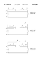
- FIGS. 1A and 1B are respective side and perspective views of a switch, in accordance with the present invention, shown in the open condition.
- FIGS. 2A and 2B are respective side and perspective views of a switch, in accordance with the present invention, shown in the closed condition.
- FIGS. 3A and 3B functionally illustrate the switch in its respective open and closed condition.
- FIG. 4A illustrates some dimensions of the switch and FIG. 4B illustrates the electrical equivalent of the switch.
- FIGS. 5A-5J illustrate the fabrication of the switch.
- FIGS. 6A and 6B illustrate another embodiment of the present invention.
- FIGS. 7A-7G illustrate the fabrication of the embodiment of the switch shown in FIGS. 6A and 6B.
- FIG. 8 is a block diagram of an overall system in which the present invention finds an application.
- FIG. 9 illustrates a time delay circuit of FIG. 8 in more detail.
- FIG. 10 illustrates, in more detail, a switch arrangement used in the time delay circuit of FIG. 9.
- FIG. 11 illustrates the capacitive coupling between mercury droplets.
- FIG. 12 is a plan view of a gate member having an electrically conductive coating thereon.
- FIG. 13 is a side view of the switch arrangement utilizing the electrically conductive coating of FIG. 12.
- switch 10 having first and second conductors 12 and 14 affixed to a substrate 16, such as alumina.
- a substrate 16 such as alumina.
- the switch is applicable to DC circuits, it will be described, by way of example, with respect to an RF circuit, and accordingly, the conductors 12 and 14 represent a 50 ohm characteristic impedance RF microstrip line, with a ground plane 18 positioned on the other side of substrate 16. Titanium/gold base layers 20 and 22 may be utilized for better adhesion of the conductors 12 and 14 to the substrate 16.
- a gate member 24 is disposed between the conductors 12 and 14 at the respective ends thereof, and includes a dielectric oxide coating 28 on the surface thereof.
- the gate member 24 is electrically conductive but has a high resistivity to prevent RF conduction and may be constituted by a polysilicon material.
- the oxide coating 28 may be silicon dioxide, or any other suitable coating such as silicon nitride, or silicon oxynitride, by way of example.
- the switch includes respective first and second mercury droplets 30 and 32 which are elongated and electrically connected to respective conductors 12 and 14 by means of bonding layers, or pads, 34 and 36.
- These bonding layers 34 and 36 are of a material, such as silver, to cause the mercury droplets to be held in place by wetting action.
- Other bonding materials include, for example, chromium, vanadium, niobium, molybdenum, tantalum and iridium.
- the RF microstrip conductors 12 and 14 are maintained at ground potential at DC or at the low frequency associated with control voltages applied to the gate member 24.
- a control electrode 40 electrically connected to gate member 24 is operable to receive a positive or negative DC control signal, relative to the mercury droplets 30 and 32, causing them to experience a lateral field to not only wet the oxide coating 28 but to pull the mercury droplets to the top of the gate member 24 where they may be physically joined, as illustrated in FIGS. 2A and 2B.
- FIGS. 3A and 3B illustrate the functional operation of the switch.
- the switch 10 In FIG. 3A with no control signal applied, the switch 10 is in an open condition and no RF signal passes between the conductors 12 and 14. With the application of, for example, a positive DC control signal (+V) of a predetermined magnitude, as illustrated in FIG. 3B, the switch assumes a closed condition to allow propagation of the RF signal.
- a positive DC control signal (+V) of a predetermined magnitude as illustrated in FIG. 3B, the switch assumes a closed condition to allow propagation of the RF signal.
- the predetermined magnitude of the control signal will depend upon the dimensions of the switch elements.
- the microstrip conductors 12 and 14 have a characteristic impedance of 50 ohms with a width of 0.0254 cm (254 ⁇ m).
- Mercury droplets 30 and 32 each have a length (into the plane of the FIG.) equal to, or slightly less than the width of the microstrip line.
- Each mercury droplet has a width d o , where d o is about 20 ⁇ m, which is approximately equal to its height as measured from the top of the droplet to the substrate 16.
- the width of the gate member 24, at its base is also assumed equal to d o .
- Equation (1) Substituting the R ON and C OFF values of 20 milliohms and 2.5 ⁇ 10 -14 farads into equation (1) yields an extremely high cutoff frequency of around 318 THz.
- FIGS. 5A through 5J illustrate one such process.
- the titanium and gold layer 20 has been applied to the top of substrate 16, and ground plane 18 been applied to the bottom thereof.
- a separator 50 as illustrated in FIG. 5B, is deposited, such as by photolithographic methods, after which the separated microstrip conductors 12 and 14 are plated, as in FIG. 5C.
- FIGS. 5D and 5E another separator 52 is formed, and bonding layers 34 and 35 are evaporated on the microstrip conductors after which the bonding layers 34 and 36 are etched to the proper size and the separators are removed, as well as the titanium/gold layer underlying the separators.
- FIG. 5H The structure of FIG. 5H is dipped into a mercury bath and removed, leaving a body of mercury 60 clinging to the bonding layers 34 and 36 and over the gate member 24. This is illustrated in FIG. 5I.
- the structure with the excess mercury is spun, as indicated by arrow 62, at about 300 rpm whereby the excess mercury is removed, leaving the well defined mercury droplets 34 and 36 as in FIG. 5J.
- the excess mercury removal may also be accomplished by electric field stripping wherein an electric field between an anode and the body of mercury pulls away the excess mercury until, as the cross section approaches 1:1, the mercury becomes stiff enough to resist further removal by field stripping.
- Another mercury deposition method includes vacuum evaporation of mercury onto a substrate using photoresist to aid in selective deposition of the mercury onto the bonding layer.
- Suitable dielectric materials may serve the role of the photoresist.
- FIGS. 6A and 6B illustrate another embodiment of the invention which is simpler to fabricate and has an even lower value of off capacitance than that previously described, resulting in a higher cut off frequency.
- Switch 70 includes a substrate 72, having a ground plane 74 on the bottom side thereof and a high sheet resistivity polysilicon layer 76 on the top side. A portion of this layer is given a localized lower resistivity, such as by diffusion, to form a gate member 78.
- a dielectric layer 80 such as a oxynitride, covers polysilicon 76, and this dielectric layer receives a titanium/gold base layer 82 to which is applied first and second microstrip conductors 84 and 86. Also applied to the titanium/gold base layer 82 are respective bonding layers, or pads, 88 and 90 for receiving respective mercury droplets 92 and 94.
- the mercury droplets 92 and 94 are as illustrated in FIG. 6A such that switch 70 is in an open condition with no RF conduction between conductors 84 and 86.
- a suitable control signal to gate member 78 as illustrated in FIG. 6B, the mercury droplets are drawn toward the gate member 78 and contact one another forming a unitary mass of mercury 96 electrically contacting both conductors 84 and 86, thus closing the switch.
- the control signal is removed, the mercury withdraws from the dielectric layer 80 and again assumes the configuration shown in FIG. 6A.
- FIGS. 7A through 7G One fabrication technique for this second switch embodiment is illustrated in FIGS. 7A through 7G.
- a substrate member 72 having a ground plane 74, has applied to the exposed surface thereof the polysilicon layer 76.
- a temporary protective oxide coating 98 is deposited on the polysilicon layer 76 by deposition or by oxidizing the surface of the polysilicon.
- the oxide coating 98 has been opened and a diffusion or ion implantation process decreases the resistivity of the polysilicon layer in a limited area, to define the gate member 78.
- the first oxide coating 98 is removed and the dielectric oxynitride layer 80 is applied, as is titanium/gold layer 82 for receiving the conductors 84 and 86, as illustrated in FIG. 7D.
- the conductors 84 and 86 may be plated on the titanium/gold layer 82 with the use of a photoresist, which has already been removed in FIG. 7D.
- FIG. 7E mercury droplet bonding pads 88 and 90 are evaporated onto the titanium/gold layer 82 and the middle section of this layer is removed leaving an exposed portion of dielectric layer 80 between the pads 88 and 90.
- the structure of FIG. 7E is dipped into a mercury bath and removed, as illustrated in FIG. 7F, leaving a body of mercury 100 clinging to the bonding layers 88 and 90 as well as to the dielectric over the gate member 78.
- Excess mercury may be removed by one of the aforementioned spin or field stripping processes leaving the switch structure of FIG. 7G. Direct vacuum evaporation of mercury onto the pads may also be accomplished.
- the switch or switches may be placed in a hermetically sealed container filled with an inert gas, such as argon, prior to use.
- This container can either be external, or an integrally constructed configuration relative to the switch.
- the mercury wetted switch of the present invention finds applicability in a variety of microwave systems, a sample one of which is illustrated in FIG. 8.
- FIG. 8 is a simplified representation of the transmitter function of a radar system having a plurality of antenna elements 110A, 110B . . . 110n.
- a transmitter 112 provides an RF signal to be transmitted, to a manifold circuit 114 which distributes the signal to the plurality of antenna elements.
- a transmitter beam, or a plurality of such beams may be formed and steered, with the provision of a delay circuit 116 comprised of a plurality of time delay units 118, and all being governed by a control means 120.
- receiver beams may be formed and steered utilizing similar delay units.
- a typical time delay unit 118 is illustrated in more detail in FIG. 9.
- the time delay unit 118 includes nine stages of delay, 121-129 which, when selectively placed into the signal path, can control the relative time delay of a signal applied to input terminal 130, from 0 ns to 2.048 ns in 4 ps increments, until the signal appears at output terminal 132.
- stage 121 is capable of a 1024 ps delay, with delays of 512 ps, 256 ps, 128 ps, 64 ps, 32 ps, 16 ps, 8 ps, and 4 ps being provided by respective stages 122-129.
- the selection of the particular stages to be in the signal path is governed by inclusion of single pole, double throw mercury wetted switch arrangements utilizing the principles described herein, and identified by reference characters 136 in FIG. 9.
- a typical switch arrangement 136 is illustrated in more detail in FIG. 10.
- a first, or input conductor 140 receives a microwave signal from a previous delay stage (or from input terminal 130, if it is the first stage).
- a first output conductor 141 will route the applied signal to a delay stage, while a second conductor 142 will route the signal to a subsequent switch 136 of a next delay stage (or to output terminal 132, if it is the last stage).
- Routing of the signal to either conductor 141 or 142 is accomplished by the provision of respective mercury switches 146 and 147, each having a construction as previously described.
- switch 146 includes a gate member 150 having a gate electrode 152 to which is applied a control signal for governing movement of mercury droplets 154 and 156 for closing switch 146, whereby conductor 141 is selected for the signal path.
- switch 147 includes a gate member 160 having a gate electrode 162 to which is applied a control signal for governing movement of the mercury droplets 164 and 166 for closing switch 147, whereby conductor 142 is selected for the signal path.
- FIGS. 2A and 6B illustrate the spaced apart mercury droplets coming into direct physical contact under the influence of a control signal applied to the gate member.
- a control signal applied to the gate member.
- mercury droplets 30 and 32 are drawn toward one another under the influence of a control signal but stop short of direct contact. Under such circumstances electrical connection may be made by means of capacitive coupling, as indicated by reference character 168.
- FIGS. 12 and 13 Another embodiment of the switch wherein the mercury droplets are drawn toward one another under the influence of a control signal but stop short of direct contact, is illustrated in FIGS. 12 and 13.
- the gate member 24 includes an electrically conducting layer 170 on the surface thereof. Electrically conducting layer 170 has a predetermined pattern which includes a series of fingers, or projections, 172. As illustrated in FIG. 13, these projections complete electrical connection between the mercury droplets 30 and 32, however without significantly blocking the field which causes the droplets to be drawn toward the gate member 24.
Abstract
Description
F.sub.CO =1/(2π×R.sub.ON ×C.sub.OFF) eq (1)
Claims (12)
Priority Applications (2)
| Application Number | Priority Date | Filing Date | Title |
|---|---|---|---|
| US09/135,747 US5912606A (en) | 1998-08-18 | 1998-08-18 | Mercury wetted switch |
| US09/271,833 US6191754B1 (en) | 1998-08-18 | 1999-03-18 | Antenna system using time delays with mercury wetted switches |
Applications Claiming Priority (1)
| Application Number | Priority Date | Filing Date | Title |
|---|---|---|---|
| US09/135,747 US5912606A (en) | 1998-08-18 | 1998-08-18 | Mercury wetted switch |
Related Child Applications (1)
| Application Number | Title | Priority Date | Filing Date |
|---|---|---|---|
| US09/271,833 Continuation-In-Part US6191754B1 (en) | 1998-08-18 | 1999-03-18 | Antenna system using time delays with mercury wetted switches |
Publications (1)
| Publication Number | Publication Date |
|---|---|
| US5912606A true US5912606A (en) | 1999-06-15 |
Family
ID=22469477
Family Applications (1)
| Application Number | Title | Priority Date | Filing Date |
|---|---|---|---|
| US09/135,747 Expired - Fee Related US5912606A (en) | 1998-08-18 | 1998-08-18 | Mercury wetted switch |
Country Status (1)
| Country | Link |
|---|---|
| US (1) | US5912606A (en) |
Cited By (81)
| Publication number | Priority date | Publication date | Assignee | Title |
|---|---|---|---|---|
| US6191754B1 (en) * | 1998-08-18 | 2001-02-20 | Northrop Grumman Corporation | Antenna system using time delays with mercury wetted switches |
| WO2001057900A1 (en) * | 2000-02-02 | 2001-08-09 | Raytheon Company | Microelectromechanical micro-relay with liquid metal contacts |
| US6373356B1 (en) * | 1999-05-21 | 2002-04-16 | Interscience, Inc. | Microelectromechanical liquid metal current carrying system, apparatus and method |
| US20030080650A1 (en) * | 2001-10-31 | 2003-05-01 | Wong Marvin Glenn | Longitudinal piezoelectric optical latching relay |
| US6559420B1 (en) * | 2002-07-10 | 2003-05-06 | Agilent Technologies, Inc. | Micro-switch heater with varying gas sub-channel cross-section |
| US20030189773A1 (en) * | 2002-03-28 | 2003-10-09 | Wong Marvin Glenn | Piezoelectric optical relay |
| US6633213B1 (en) * | 2002-04-24 | 2003-10-14 | Agilent Technologies, Inc. | Double sided liquid metal micro switch |
| US20030194170A1 (en) * | 2002-04-10 | 2003-10-16 | Wong Marvin Glenn | Piezoelectric optical demultiplexing switch |
| US6717495B2 (en) * | 2001-02-23 | 2004-04-06 | Agilent Technologies, Inc. | Conductive liquid-based latching switch device |
| US20040066259A1 (en) * | 2002-10-08 | 2004-04-08 | Dove Lewis R. | Electrically isolated liquid metal micro-switches for integrally shielded microcircuits |
| US6730866B1 (en) | 2003-04-14 | 2004-05-04 | Agilent Technologies, Inc. | High-frequency, liquid metal, latching relay array |
| US6740829B1 (en) | 2003-04-14 | 2004-05-25 | Agilent Technologies, Inc. | Insertion-type liquid metal latching relay |
| US6743990B1 (en) | 2002-12-12 | 2004-06-01 | Agilent Technologies, Inc. | Volume adjustment apparatus and method for use |
| US6747222B1 (en) | 2003-02-04 | 2004-06-08 | Agilent Technologies, Inc. | Feature formation in a nonphotoimagable material and switch incorporating same |
| US6750594B2 (en) | 2002-05-02 | 2004-06-15 | Agilent Technologies, Inc. | Piezoelectrically actuated liquid metal switch |
| US6750413B1 (en) | 2003-04-25 | 2004-06-15 | Agilent Technologies, Inc. | Liquid metal micro switches using patterned thick film dielectric as channels and a thin ceramic or glass cover plate |
| US20040112727A1 (en) * | 2002-12-12 | 2004-06-17 | Wong Marvin Glenn | Laser cut channel plate for a switch |
| US20040112726A1 (en) * | 2002-12-12 | 2004-06-17 | Wong Marvin Glenn | Ultrasonically milled channel plate for a switch |
| US20040112729A1 (en) * | 2002-12-12 | 2004-06-17 | Wong Marvin Glenn | Switch and method for producing the same |
| US20040112728A1 (en) * | 2002-12-12 | 2004-06-17 | Wong Marvin Glenn | Ceramic channel plate for a switch |
| US6756551B2 (en) | 2002-05-09 | 2004-06-29 | Agilent Technologies, Inc. | Piezoelectrically actuated liquid metal switch |
| US6759611B1 (en) | 2003-06-16 | 2004-07-06 | Agilent Technologies, Inc. | Fluid-based switches and methods for producing the same |
| US6759610B1 (en) | 2003-06-05 | 2004-07-06 | Agilent Technologies, Inc. | Multi-layer assembly of stacked LIMMS devices with liquid metal vias |
| US6762378B1 (en) | 2003-04-14 | 2004-07-13 | Agilent Technologies, Inc. | Liquid metal, latching relay with face contact |
| US6765161B1 (en) | 2003-04-14 | 2004-07-20 | Agilent Technologies, Inc. | Method and structure for a slug caterpillar piezoelectric latching reflective optical relay |
| US20040140187A1 (en) * | 2003-01-22 | 2004-07-22 | Wong Marvin Glenn | Method for registering a deposited material with channel plate channels, and switch produced using same |
| US6768068B1 (en) | 2003-04-14 | 2004-07-27 | Agilent Technologies, Inc. | Method and structure for a slug pusher-mode piezoelectrically actuated liquid metal switch |
| US20040144632A1 (en) * | 2003-01-13 | 2004-07-29 | Wong Marvin Glenn | Photoimaged channel plate for a switch |
| US6770827B1 (en) | 2003-04-14 | 2004-08-03 | Agilent Technologies, Inc. | Electrical isolation of fluid-based switches |
| US6774324B2 (en) | 2002-12-12 | 2004-08-10 | Agilent Technologies, Inc. | Switch and production thereof |
| US6774325B1 (en) | 2003-04-14 | 2004-08-10 | Agilent Technologies, Inc. | Reducing oxides on a switching fluid in a fluid-based switch |
| US6777630B1 (en) | 2003-04-30 | 2004-08-17 | Agilent Technologies, Inc. | Liquid metal micro switches using as channels and heater cavities matching patterned thick film dielectric layers on opposing thin ceramic plates |
| US6781074B1 (en) | 2003-07-30 | 2004-08-24 | Agilent Technologies, Inc. | Preventing corrosion degradation in a fluid-based switch |
| US6787720B1 (en) | 2003-07-31 | 2004-09-07 | Agilent Technologies, Inc. | Gettering agent and method to prevent corrosion in a fluid switch |
| US6794591B1 (en) | 2003-04-14 | 2004-09-21 | Agilent Technologies, Inc. | Fluid-based switches |
| US6798937B1 (en) | 2003-04-14 | 2004-09-28 | Agilent Technologies, Inc. | Pressure actuated solid slug optical latching relay |
| US20040188234A1 (en) * | 2003-03-31 | 2004-09-30 | Dove Lewis R. | Hermetic seal and controlled impedance rf connections for a liquid metal micro switch |
| US6803842B1 (en) | 2003-04-14 | 2004-10-12 | Agilent Technologies, Inc. | Longitudinal mode solid slug optical latching relay |
| US20040202413A1 (en) * | 2003-04-14 | 2004-10-14 | Wong Marvin Glenn | Method and structure for a solid slug caterpillar piezoelectric optical relay |
| US20040201440A1 (en) * | 2003-04-14 | 2004-10-14 | Arthur Fong | Longitudinal electromagnetic latching relay |
| US20040201329A1 (en) * | 2003-04-14 | 2004-10-14 | Wong Marvin Glenn | Damped longitudinal mode latching relay |
| US20040200708A1 (en) * | 2003-04-14 | 2004-10-14 | Wong Marvin Glenn | Method and structure for a slug assisted pusher-mode piezoelectrically actuated liquid metal optical switch |
| US20040201323A1 (en) * | 2003-04-14 | 2004-10-14 | Wong Marvin Glenn | Shear mode liquid metal switch |
| US20040200707A1 (en) * | 2003-04-14 | 2004-10-14 | Wong Marvin Glenn | Bent switching fluid cavity |
| US20040200706A1 (en) * | 2003-04-14 | 2004-10-14 | Dove Lewis R. | Substrate with liquid electrode |
| US20040201310A1 (en) * | 2003-04-14 | 2004-10-14 | Wong Marvin Glenn | Damped longitudinal mode optical latching relay |
| US20040202404A1 (en) * | 2003-04-14 | 2004-10-14 | Wong Marvin Glenn | Polymeric liquid metal optical switch |
| US20040200703A1 (en) * | 2003-04-14 | 2004-10-14 | Wong Marvin Glenn | Bending mode liquid metal switch |
| US20040201315A1 (en) * | 2003-04-14 | 2004-10-14 | Wong Marvin Glenn | Bending-mode latching relay |
| US20040202414A1 (en) * | 2003-04-14 | 2004-10-14 | Wong Marvin Glenn | Reflecting wedge optical wavelength multiplexer/demultiplexer |
| US20040201311A1 (en) * | 2003-04-14 | 2004-10-14 | Wong Marvin Glenn | High frequency bending-mode latching relay |
| US20040201317A1 (en) * | 2003-04-14 | 2004-10-14 | Wong Marvin Glenn | Method and structure for a pusher-mode piezoelectrically actuated liquid switch metal switch |
| US20040201322A1 (en) * | 2003-04-14 | 2004-10-14 | Wong Marvin Glenn | Longitudinal mode optical latching relay |
| US20040200702A1 (en) * | 2003-04-14 | 2004-10-14 | Arthur Fong | Push-mode latching relay |
| US20040201447A1 (en) * | 2003-04-14 | 2004-10-14 | Wong Marvin Glenn | Thin-film resistor device |
| US20040201314A1 (en) * | 2003-04-14 | 2004-10-14 | Wong Marvin Glenn | Wetting finger latching piezoelectric relay |
| US20040201319A1 (en) * | 2003-04-14 | 2004-10-14 | Wong Marvin Glenn | High frequency push-mode latching relay |
| US20040202558A1 (en) * | 2003-04-14 | 2004-10-14 | Arthur Fong | Closed-loop piezoelectric pump |
| US20040201316A1 (en) * | 2003-04-14 | 2004-10-14 | Arthur Fong | Method and structure for a solid slug caterpillar piezoelectric relay |
| US20040201312A1 (en) * | 2003-04-14 | 2004-10-14 | Arthur Fong | Method and structure for a slug assisted longitudinal piezoelectrically actuated liquid metal optical switch |
| US20040201313A1 (en) * | 2003-04-14 | 2004-10-14 | Wong Marvin Glenn | High-frequency, liquid metal, latching relay with face contact |
| US20040201330A1 (en) * | 2003-04-14 | 2004-10-14 | Arthur Fong | Method and apparatus for maintaining a liquid metal switch in a ready-to-switch condition |
| US20040200704A1 (en) * | 2003-04-14 | 2004-10-14 | Arthur Fong | Fluid-based switch |
| US20040202844A1 (en) * | 2003-04-14 | 2004-10-14 | Wong Marvin Glenn | Feature formation in thick-film inks |
| US20040201309A1 (en) * | 2003-04-14 | 2004-10-14 | Wong Marvin Glenn | Insertion-type liquid metal latching relay array |
| US20040200705A1 (en) * | 2003-04-14 | 2004-10-14 | Wong Marvin Glenn | Formation of signal paths to increase maximum signal-carrying frequency of a fluid-based switch |
| US20040201907A1 (en) * | 2003-04-14 | 2004-10-14 | Wong Marvin Glenn | Liquid metal optical relay |
| US20040202410A1 (en) * | 2003-04-14 | 2004-10-14 | Wong Marvin Glenn | Longitudinal electromagnetic latching optical relay |
| US20040202411A1 (en) * | 2003-04-14 | 2004-10-14 | Wong Marvin Glenn | Method and structure for a pusher-mode piezoelectrically actuated liquid metal optical switch |
| US20040201320A1 (en) * | 2003-04-14 | 2004-10-14 | Carson Paul Thomas | Inserting-finger liquid metal relay |
| US20040202408A1 (en) * | 2003-04-14 | 2004-10-14 | Wong Marvin Glenn | Pressure actuated optical latching relay |
| US20040201318A1 (en) * | 2003-04-14 | 2004-10-14 | Wong Marvin Glen | Latching relay with switch bar |
| US20040201321A1 (en) * | 2003-04-14 | 2004-10-14 | Wong Marvin Glenn | High frequency latching relay with bending switch bar |
| US20040251117A1 (en) * | 2003-06-16 | 2004-12-16 | Wong Marvin Glenn | Suspended thin-film resistor |
| US20050034962A1 (en) * | 2003-04-14 | 2005-02-17 | Wong Marvin Glenn | Reducing oxides on a switching fluid in a fluid-based switch |
| US6927529B2 (en) | 2002-05-02 | 2005-08-09 | Agilent Technologies, Inc. | Solid slug longitudinal piezoelectric latching relay |
| EP1583128A1 (en) * | 2004-04-01 | 2005-10-05 | Lucent Technologies Inc. | Liquid electrical microswitch |
| US20050263379A1 (en) * | 2003-04-14 | 2005-12-01 | John Ralph Lindsey | Reduction of oxides in a fluid-based switch |
| WO2005114740A1 (en) | 2004-05-21 | 2005-12-01 | University Of Cincinnati | Liquid logic structures for electronic device applications |
| US20070216497A1 (en) * | 2006-03-14 | 2007-09-20 | Lucent Technologies Inc. | Method and apparatus for signal processing using electrowetting |
| US7280386B2 (en) | 2004-07-15 | 2007-10-09 | Micron Technology, Inc. | Method and system for controlling refresh to avoid memory cell data losses |
Citations (4)
| Publication number | Priority date | Publication date | Assignee | Title |
|---|---|---|---|---|
| US2312672A (en) * | 1941-05-09 | 1943-03-02 | Bell Telephone Labor Inc | Switching device |
| US3144533A (en) * | 1962-03-16 | 1964-08-11 | Fifth Dimension Inc | Mercury relay |
| US3198919A (en) * | 1962-08-01 | 1965-08-03 | Bendix Corp | Mercury switch |
| US3906415A (en) * | 1974-06-14 | 1975-09-16 | Massachusetts Inst Technology | Apparatus wherein a segmented fluid stream performs electrical switching functions and the like |
-
1998
- 1998-08-18 US US09/135,747 patent/US5912606A/en not_active Expired - Fee Related
Patent Citations (4)
| Publication number | Priority date | Publication date | Assignee | Title |
|---|---|---|---|---|
| US2312672A (en) * | 1941-05-09 | 1943-03-02 | Bell Telephone Labor Inc | Switching device |
| US3144533A (en) * | 1962-03-16 | 1964-08-11 | Fifth Dimension Inc | Mercury relay |
| US3198919A (en) * | 1962-08-01 | 1965-08-03 | Bendix Corp | Mercury switch |
| US3906415A (en) * | 1974-06-14 | 1975-09-16 | Massachusetts Inst Technology | Apparatus wherein a segmented fluid stream performs electrical switching functions and the like |
Cited By (146)
| Publication number | Priority date | Publication date | Assignee | Title |
|---|---|---|---|---|
| US6191754B1 (en) * | 1998-08-18 | 2001-02-20 | Northrop Grumman Corporation | Antenna system using time delays with mercury wetted switches |
| US6501354B1 (en) | 1999-05-21 | 2002-12-31 | Interscience, Inc. | Microelectromechanical liquid metal current carrying system, apparatus and method |
| US6373356B1 (en) * | 1999-05-21 | 2002-04-16 | Interscience, Inc. | Microelectromechanical liquid metal current carrying system, apparatus and method |
| US6864767B2 (en) | 2000-02-02 | 2005-03-08 | Raytheon Company | Microelectromechanical micro-relay with liquid metal contacts |
| CN100483592C (en) * | 2000-02-02 | 2009-04-29 | 雷声公司 | Microelectromechanical micro-relay with liquid metal contacts |
| US6396371B2 (en) | 2000-02-02 | 2002-05-28 | Raytheon Company | Microelectromechanical micro-relay with liquid metal contacts |
| WO2001057900A1 (en) * | 2000-02-02 | 2001-08-09 | Raytheon Company | Microelectromechanical micro-relay with liquid metal contacts |
| US20020105396A1 (en) * | 2000-02-02 | 2002-08-08 | Streeter Robert D. | Microelectromechanical micro-relay with liquid metal contacts |
| US6717495B2 (en) * | 2001-02-23 | 2004-04-06 | Agilent Technologies, Inc. | Conductive liquid-based latching switch device |
| US20030080650A1 (en) * | 2001-10-31 | 2003-05-01 | Wong Marvin Glenn | Longitudinal piezoelectric optical latching relay |
| US7078849B2 (en) | 2001-10-31 | 2006-07-18 | Agilent Technologies, Inc. | Longitudinal piezoelectric optical latching relay |
| US20030189773A1 (en) * | 2002-03-28 | 2003-10-09 | Wong Marvin Glenn | Piezoelectric optical relay |
| US6741767B2 (en) | 2002-03-28 | 2004-05-25 | Agilent Technologies, Inc. | Piezoelectric optical relay |
| US20030194170A1 (en) * | 2002-04-10 | 2003-10-16 | Wong Marvin Glenn | Piezoelectric optical demultiplexing switch |
| US6633213B1 (en) * | 2002-04-24 | 2003-10-14 | Agilent Technologies, Inc. | Double sided liquid metal micro switch |
| US6927529B2 (en) | 2002-05-02 | 2005-08-09 | Agilent Technologies, Inc. | Solid slug longitudinal piezoelectric latching relay |
| US6750594B2 (en) | 2002-05-02 | 2004-06-15 | Agilent Technologies, Inc. | Piezoelectrically actuated liquid metal switch |
| US6756551B2 (en) | 2002-05-09 | 2004-06-29 | Agilent Technologies, Inc. | Piezoelectrically actuated liquid metal switch |
| US6559420B1 (en) * | 2002-07-10 | 2003-05-06 | Agilent Technologies, Inc. | Micro-switch heater with varying gas sub-channel cross-section |
| US20040066259A1 (en) * | 2002-10-08 | 2004-04-08 | Dove Lewis R. | Electrically isolated liquid metal micro-switches for integrally shielded microcircuits |
| US6781075B2 (en) | 2002-10-08 | 2004-08-24 | Agilent Technologies, Inc. | Electrically isolated liquid metal micro-switches for integrally shielded microcircuits |
| US20040112729A1 (en) * | 2002-12-12 | 2004-06-17 | Wong Marvin Glenn | Switch and method for producing the same |
| US6774324B2 (en) | 2002-12-12 | 2004-08-10 | Agilent Technologies, Inc. | Switch and production thereof |
| US20040112724A1 (en) * | 2002-12-12 | 2004-06-17 | Wong Marvin Glenn | Volume adjustment apparatus and method for use |
| US20040112728A1 (en) * | 2002-12-12 | 2004-06-17 | Wong Marvin Glenn | Ceramic channel plate for a switch |
| US20040112726A1 (en) * | 2002-12-12 | 2004-06-17 | Wong Marvin Glenn | Ultrasonically milled channel plate for a switch |
| US7022926B2 (en) | 2002-12-12 | 2006-04-04 | Agilent Technologies, Inc. | Ultrasonically milled channel plate for a switch |
| US20050000620A1 (en) * | 2002-12-12 | 2005-01-06 | Wong Marvin Glenn | Method for making switch with ultrasonically milled channel plate |
| US20040112727A1 (en) * | 2002-12-12 | 2004-06-17 | Wong Marvin Glenn | Laser cut channel plate for a switch |
| US6924444B2 (en) | 2002-12-12 | 2005-08-02 | Agilent Technologies, Inc. | Ceramic channel plate for a fluid-based switch, and method for making same |
| US20050000784A1 (en) * | 2002-12-12 | 2005-01-06 | Wong Marvin Glenn | Liquid switch production and assembly |
| US6849144B2 (en) | 2002-12-12 | 2005-02-01 | Agilent Technologies, Inc. | Method for making switch with ultrasonically milled channel plate |
| US6855898B2 (en) | 2002-12-12 | 2005-02-15 | Agilent Technologies, Inc. | Ceramic channel plate for a switch |
| US6909059B2 (en) | 2002-12-12 | 2005-06-21 | Agilent Technologies, Inc. | Liquid switch production and assembly |
| US6743990B1 (en) | 2002-12-12 | 2004-06-01 | Agilent Technologies, Inc. | Volume adjustment apparatus and method for use |
| US20050126899A1 (en) * | 2003-01-13 | 2005-06-16 | Wong Marvin G. | Photoimaged channel plate for a switch, and method for making a switch using same |
| US6897387B2 (en) | 2003-01-13 | 2005-05-24 | Agilent Technologies, Inc. | Photoimaged channel plate for a switch |
| US7098413B2 (en) | 2003-01-13 | 2006-08-29 | Agilent Technologies, Inc. | Photoimaged channel plate for a switch, and method for making a switch using same |
| US20040144632A1 (en) * | 2003-01-13 | 2004-07-29 | Wong Marvin Glenn | Photoimaged channel plate for a switch |
| US7019235B2 (en) | 2003-01-13 | 2006-03-28 | Agilent Technologies, Inc. | Photoimaged channel plate for a switch |
| US6809277B2 (en) | 2003-01-22 | 2004-10-26 | Agilent Technologies, Inc. | Method for registering a deposited material with channel plate channels, and switch produced using same |
| US6911611B2 (en) | 2003-01-22 | 2005-06-28 | Agilent Technologies, Inc. | Method for registering a deposited material with channel plate channels |
| US20040140187A1 (en) * | 2003-01-22 | 2004-07-22 | Wong Marvin Glenn | Method for registering a deposited material with channel plate channels, and switch produced using same |
| US6747222B1 (en) | 2003-02-04 | 2004-06-08 | Agilent Technologies, Inc. | Feature formation in a nonphotoimagable material and switch incorporating same |
| US20040188234A1 (en) * | 2003-03-31 | 2004-09-30 | Dove Lewis R. | Hermetic seal and controlled impedance rf connections for a liquid metal micro switch |
| US6825429B2 (en) | 2003-03-31 | 2004-11-30 | Agilent Technologies, Inc. | Hermetic seal and controlled impedance RF connections for a liquid metal micro switch |
| US6894237B2 (en) | 2003-04-14 | 2005-05-17 | Agilent Technologies, Inc. | Formation of signal paths to increase maximum signal-carrying frequency of a fluid-based switch |
| US6870111B2 (en) | 2003-04-14 | 2005-03-22 | Agilent Technologies, Inc. | Bending mode liquid metal switch |
| US20040200708A1 (en) * | 2003-04-14 | 2004-10-14 | Wong Marvin Glenn | Method and structure for a slug assisted pusher-mode piezoelectrically actuated liquid metal optical switch |
| US20040201323A1 (en) * | 2003-04-14 | 2004-10-14 | Wong Marvin Glenn | Shear mode liquid metal switch |
| US20040200707A1 (en) * | 2003-04-14 | 2004-10-14 | Wong Marvin Glenn | Bent switching fluid cavity |
| US20040200706A1 (en) * | 2003-04-14 | 2004-10-14 | Dove Lewis R. | Substrate with liquid electrode |
| US20040201310A1 (en) * | 2003-04-14 | 2004-10-14 | Wong Marvin Glenn | Damped longitudinal mode optical latching relay |
| US20040202404A1 (en) * | 2003-04-14 | 2004-10-14 | Wong Marvin Glenn | Polymeric liquid metal optical switch |
| US20040202412A1 (en) * | 2003-04-14 | 2004-10-14 | Wong Marvin Glenn | Pressure actuated solid slug optical latching relay |
| US20040200703A1 (en) * | 2003-04-14 | 2004-10-14 | Wong Marvin Glenn | Bending mode liquid metal switch |
| US20040201315A1 (en) * | 2003-04-14 | 2004-10-14 | Wong Marvin Glenn | Bending-mode latching relay |
| US20040202414A1 (en) * | 2003-04-14 | 2004-10-14 | Wong Marvin Glenn | Reflecting wedge optical wavelength multiplexer/demultiplexer |
| US20040201311A1 (en) * | 2003-04-14 | 2004-10-14 | Wong Marvin Glenn | High frequency bending-mode latching relay |
| US20040201317A1 (en) * | 2003-04-14 | 2004-10-14 | Wong Marvin Glenn | Method and structure for a pusher-mode piezoelectrically actuated liquid switch metal switch |
| US20040201322A1 (en) * | 2003-04-14 | 2004-10-14 | Wong Marvin Glenn | Longitudinal mode optical latching relay |
| US20040200702A1 (en) * | 2003-04-14 | 2004-10-14 | Arthur Fong | Push-mode latching relay |
| US20040201447A1 (en) * | 2003-04-14 | 2004-10-14 | Wong Marvin Glenn | Thin-film resistor device |
| US20040201314A1 (en) * | 2003-04-14 | 2004-10-14 | Wong Marvin Glenn | Wetting finger latching piezoelectric relay |
| US20040201319A1 (en) * | 2003-04-14 | 2004-10-14 | Wong Marvin Glenn | High frequency push-mode latching relay |
| US20040202558A1 (en) * | 2003-04-14 | 2004-10-14 | Arthur Fong | Closed-loop piezoelectric pump |
| US20040201316A1 (en) * | 2003-04-14 | 2004-10-14 | Arthur Fong | Method and structure for a solid slug caterpillar piezoelectric relay |
| US20040201312A1 (en) * | 2003-04-14 | 2004-10-14 | Arthur Fong | Method and structure for a slug assisted longitudinal piezoelectrically actuated liquid metal optical switch |
| US20040201313A1 (en) * | 2003-04-14 | 2004-10-14 | Wong Marvin Glenn | High-frequency, liquid metal, latching relay with face contact |
| US20040201330A1 (en) * | 2003-04-14 | 2004-10-14 | Arthur Fong | Method and apparatus for maintaining a liquid metal switch in a ready-to-switch condition |
| US20040200704A1 (en) * | 2003-04-14 | 2004-10-14 | Arthur Fong | Fluid-based switch |
| US20040202844A1 (en) * | 2003-04-14 | 2004-10-14 | Wong Marvin Glenn | Feature formation in thick-film inks |
| US20040201309A1 (en) * | 2003-04-14 | 2004-10-14 | Wong Marvin Glenn | Insertion-type liquid metal latching relay array |
| US20040200705A1 (en) * | 2003-04-14 | 2004-10-14 | Wong Marvin Glenn | Formation of signal paths to increase maximum signal-carrying frequency of a fluid-based switch |
| US20040201907A1 (en) * | 2003-04-14 | 2004-10-14 | Wong Marvin Glenn | Liquid metal optical relay |
| US20040202410A1 (en) * | 2003-04-14 | 2004-10-14 | Wong Marvin Glenn | Longitudinal electromagnetic latching optical relay |
| US20040202411A1 (en) * | 2003-04-14 | 2004-10-14 | Wong Marvin Glenn | Method and structure for a pusher-mode piezoelectrically actuated liquid metal optical switch |
| US20040201320A1 (en) * | 2003-04-14 | 2004-10-14 | Carson Paul Thomas | Inserting-finger liquid metal relay |
| US20040202408A1 (en) * | 2003-04-14 | 2004-10-14 | Wong Marvin Glenn | Pressure actuated optical latching relay |
| US20040201318A1 (en) * | 2003-04-14 | 2004-10-14 | Wong Marvin Glen | Latching relay with switch bar |
| US20040201321A1 (en) * | 2003-04-14 | 2004-10-14 | Wong Marvin Glenn | High frequency latching relay with bending switch bar |
| US20040201906A1 (en) * | 2003-04-14 | 2004-10-14 | Wong Marvin Glenn | Longitudinal mode solid slug optical latching relay |
| US6816641B2 (en) | 2003-04-14 | 2004-11-09 | Agilent Technologies, Inc. | Method and structure for a solid slug caterpillar piezoelectric optical relay |
| US6818844B2 (en) | 2003-04-14 | 2004-11-16 | Agilent Technologies, Inc. | Method and structure for a slug assisted pusher-mode piezoelectrically actuated liquid metal optical switch |
| US20040201440A1 (en) * | 2003-04-14 | 2004-10-14 | Arthur Fong | Longitudinal electromagnetic latching relay |
| US6831532B2 (en) | 2003-04-14 | 2004-12-14 | Agilent Technologies, Inc. | Push-mode latching relay |
| US6730866B1 (en) | 2003-04-14 | 2004-05-04 | Agilent Technologies, Inc. | High-frequency, liquid metal, latching relay array |
| US6740829B1 (en) | 2003-04-14 | 2004-05-25 | Agilent Technologies, Inc. | Insertion-type liquid metal latching relay |
| US6838959B2 (en) | 2003-04-14 | 2005-01-04 | Agilent Technologies, Inc. | Longitudinal electromagnetic latching relay |
| US20040202413A1 (en) * | 2003-04-14 | 2004-10-14 | Wong Marvin Glenn | Method and structure for a solid slug caterpillar piezoelectric optical relay |
| US6803842B1 (en) | 2003-04-14 | 2004-10-12 | Agilent Technologies, Inc. | Longitudinal mode solid slug optical latching relay |
| US6841746B2 (en) | 2003-04-14 | 2005-01-11 | Agilent Technologies, Inc. | Bent switching fluid cavity |
| US6798937B1 (en) | 2003-04-14 | 2004-09-28 | Agilent Technologies, Inc. | Pressure actuated solid slug optical latching relay |
| US6794591B1 (en) | 2003-04-14 | 2004-09-21 | Agilent Technologies, Inc. | Fluid-based switches |
| US20050034962A1 (en) * | 2003-04-14 | 2005-02-17 | Wong Marvin Glenn | Reducing oxides on a switching fluid in a fluid-based switch |
| US7071432B2 (en) | 2003-04-14 | 2006-07-04 | Agilent Technologies, Inc. | Reduction of oxides in a fluid-based switch |
| US20040201329A1 (en) * | 2003-04-14 | 2004-10-14 | Wong Marvin Glenn | Damped longitudinal mode latching relay |
| US6872904B2 (en) | 2003-04-14 | 2005-03-29 | Agilent Technologies, Inc. | Fluid-based switch |
| US6876133B2 (en) | 2003-04-14 | 2005-04-05 | Agilent Technologies, Inc. | Latching relay with switch bar |
| US6876131B2 (en) | 2003-04-14 | 2005-04-05 | Agilent Technologies, Inc. | High-frequency, liquid metal, latching relay with face contact |
| US6876132B2 (en) | 2003-04-14 | 2005-04-05 | Agilent Technologies, Inc. | Method and structure for a solid slug caterpillar piezoelectric relay |
| US6879088B2 (en) | 2003-04-14 | 2005-04-12 | Agilent Technologies, Inc. | Insertion-type liquid metal latching relay array |
| US6879089B2 (en) | 2003-04-14 | 2005-04-12 | Agilent Technologies, Inc. | Damped longitudinal mode optical latching relay |
| US6882088B2 (en) | 2003-04-14 | 2005-04-19 | Agilent Technologies, Inc. | Bending-mode latching relay |
| US6885133B2 (en) | 2003-04-14 | 2005-04-26 | Agilent Technologies, Inc. | High frequency bending-mode latching relay |
| US6888977B2 (en) | 2003-04-14 | 2005-05-03 | Agilent Technologies, Inc. | Polymeric liquid metal optical switch |
| US6891315B2 (en) | 2003-04-14 | 2005-05-10 | Agilent Technologies, Inc. | Shear mode liquid metal switch |
| US6891116B2 (en) | 2003-04-14 | 2005-05-10 | Agilent Technologies, Inc. | Substrate with liquid electrode |
| US7070908B2 (en) | 2003-04-14 | 2006-07-04 | Agilent Technologies, Inc. | Feature formation in thick-film inks |
| US6894424B2 (en) | 2003-04-14 | 2005-05-17 | Agilent Technologies, Inc. | High frequency push-mode latching relay |
| US7048519B2 (en) | 2003-04-14 | 2006-05-23 | Agilent Technologies, Inc. | Closed-loop piezoelectric pump |
| US6900578B2 (en) | 2003-04-14 | 2005-05-31 | Agilent Technologies, Inc. | High frequency latching relay with bending switch bar |
| US6903492B2 (en) | 2003-04-14 | 2005-06-07 | Agilent Technologies, Inc. | Wetting finger latching piezoelectric relay |
| US6903490B2 (en) | 2003-04-14 | 2005-06-07 | Agilent Technologies, Inc. | Longitudinal mode optical latching relay |
| US6903493B2 (en) | 2003-04-14 | 2005-06-07 | Agilent Technologies, Inc. | Inserting-finger liquid metal relay |
| US6903287B2 (en) | 2003-04-14 | 2005-06-07 | Agilent Technologies, Inc. | Liquid metal optical relay |
| US6906271B2 (en) | 2003-04-14 | 2005-06-14 | Agilent Technologies, Inc. | Fluid-based switch |
| US6774325B1 (en) | 2003-04-14 | 2004-08-10 | Agilent Technologies, Inc. | Reducing oxides on a switching fluid in a fluid-based switch |
| US6770827B1 (en) | 2003-04-14 | 2004-08-03 | Agilent Technologies, Inc. | Electrical isolation of fluid-based switches |
| US6768068B1 (en) | 2003-04-14 | 2004-07-27 | Agilent Technologies, Inc. | Method and structure for a slug pusher-mode piezoelectrically actuated liquid metal switch |
| US6920259B2 (en) | 2003-04-14 | 2005-07-19 | Agilent Technologies, Inc. | Longitudinal electromagnetic latching optical relay |
| US6924443B2 (en) | 2003-04-14 | 2005-08-02 | Agilent Technologies, Inc. | Reducing oxides on a switching fluid in a fluid-based switch |
| US6765161B1 (en) | 2003-04-14 | 2004-07-20 | Agilent Technologies, Inc. | Method and structure for a slug caterpillar piezoelectric latching reflective optical relay |
| US6925223B2 (en) | 2003-04-14 | 2005-08-02 | Agilent Technologies, Inc. | Pressure actuated optical latching relay |
| US6762378B1 (en) | 2003-04-14 | 2004-07-13 | Agilent Technologies, Inc. | Liquid metal, latching relay with face contact |
| US7012354B2 (en) | 2003-04-14 | 2006-03-14 | Agilent Technologies, Inc. | Method and structure for a pusher-mode piezoelectrically actuated liquid metal switch |
| US6956990B2 (en) | 2003-04-14 | 2005-10-18 | Agilent Technologies, Inc. | Reflecting wedge optical wavelength multiplexer/demultiplexer |
| US6961487B2 (en) | 2003-04-14 | 2005-11-01 | Agilent Technologies, Inc. | Method and structure for a pusher-mode piezoelectrically actuated liquid metal optical switch |
| US20050263379A1 (en) * | 2003-04-14 | 2005-12-01 | John Ralph Lindsey | Reduction of oxides in a fluid-based switch |
| US6750413B1 (en) | 2003-04-25 | 2004-06-15 | Agilent Technologies, Inc. | Liquid metal micro switches using patterned thick film dielectric as channels and a thin ceramic or glass cover plate |
| US6777630B1 (en) | 2003-04-30 | 2004-08-17 | Agilent Technologies, Inc. | Liquid metal micro switches using as channels and heater cavities matching patterned thick film dielectric layers on opposing thin ceramic plates |
| US6759610B1 (en) | 2003-06-05 | 2004-07-06 | Agilent Technologies, Inc. | Multi-layer assembly of stacked LIMMS devices with liquid metal vias |
| US6833520B1 (en) | 2003-06-16 | 2004-12-21 | Agilent Technologies, Inc. | Suspended thin-film resistor |
| US6759611B1 (en) | 2003-06-16 | 2004-07-06 | Agilent Technologies, Inc. | Fluid-based switches and methods for producing the same |
| US20040251117A1 (en) * | 2003-06-16 | 2004-12-16 | Wong Marvin Glenn | Suspended thin-film resistor |
| US6781074B1 (en) | 2003-07-30 | 2004-08-24 | Agilent Technologies, Inc. | Preventing corrosion degradation in a fluid-based switch |
| US6787720B1 (en) | 2003-07-31 | 2004-09-07 | Agilent Technologies, Inc. | Gettering agent and method to prevent corrosion in a fluid switch |
| EP1583128A1 (en) * | 2004-04-01 | 2005-10-05 | Lucent Technologies Inc. | Liquid electrical microswitch |
| EP1751802A4 (en) * | 2004-05-21 | 2007-06-13 | Univ Cincinnati | Liquid logic structures for electronic device applications |
| EP1751802A1 (en) * | 2004-05-21 | 2007-02-14 | University Of Cincinnati | Liquid logic structures for electronic device applications |
| US20070221484A1 (en) * | 2004-05-21 | 2007-09-27 | The University Of Cincinnati | Liquid Logic Structures for Electronic Device Applications |
| WO2005114740A1 (en) | 2004-05-21 | 2005-12-01 | University Of Cincinnati | Liquid logic structures for electronic device applications |
| US8089013B2 (en) | 2004-05-21 | 2012-01-03 | University Of Cincinnati | Liquid logic structures for electronic device applications |
| US7280386B2 (en) | 2004-07-15 | 2007-10-09 | Micron Technology, Inc. | Method and system for controlling refresh to avoid memory cell data losses |
| US20070216497A1 (en) * | 2006-03-14 | 2007-09-20 | Lucent Technologies Inc. | Method and apparatus for signal processing using electrowetting |
| US7358833B2 (en) * | 2006-03-14 | 2008-04-15 | Lucent Technologies Inc. | Method and apparatus for signal processing using electrowetting |
Similar Documents
| Publication | Publication Date | Title |
|---|---|---|
| US5912606A (en) | Mercury wetted switch | |
| US6069540A (en) | Micro-electro system (MEMS) switch | |
| US6218911B1 (en) | Planar airbridge RF terminal MEMS switch | |
| US6698082B2 (en) | Micro-electromechanical switch fabricated by simultaneous formation of a resistor and bottom electrode | |
| US6016092A (en) | Miniature electromagnetic microwave switches and switch arrays | |
| US6307452B1 (en) | Folded spring based micro electromechanical (MEM) RF switch | |
| US6440767B1 (en) | Monolithic single pole double throw RF MEMS switch | |
| US7122942B2 (en) | Electrostatic RF MEMS switches | |
| US8120443B2 (en) | Radiofrequency or hyperfrequency circulator | |
| WO2006011239A1 (en) | Capacitive mems device and process for fabricating same, and high-frequency device | |
| US5994982A (en) | MEMS switched resonators for VCO applications | |
| US6949985B2 (en) | Electrostatically actuated microwave MEMS switch | |
| USRE45704E1 (en) | MEMS millimeter wave switches | |
| US7297571B2 (en) | Electrostatically actuated low response time power commutation micro-switches | |
| EP0892419B1 (en) | Micro electro-mechanical system (MEMS) switch | |
| JP3137112B2 (en) | Micromachine switch and method of manufacturing the same | |
| Shen et al. | Broadband low actuation voltage RF MEM switches | |
| US7960662B2 (en) | Radiofrequency or hyperfrequency micro-switch structure and method for producing one such structure | |
| WO2003015128A2 (en) | An electromechanical switch and method of fabrication | |
| US6191754B1 (en) | Antenna system using time delays with mercury wetted switches | |
| EP1573769B1 (en) | Microelectromechanical rf switch | |
| KR100308054B1 (en) | micro switches and fabrication method of the same | |
| KR20020074331A (en) | MEMS Switch using RF Blocking Resistor | |
| CN115249601A (en) | Micro-electromechanical system switch and preparation method thereof |
Legal Events
| Date | Code | Title | Description |
|---|---|---|---|
| AS | Assignment |
Owner name: NORTHROP GRUMMAN CORPORATION, MARYLAND Free format text: ASSIGNMENT OF ASSIGNORS INTEREST;ASSIGNORS:NATHANSON, HARVEY C.;SMITH, THOMAS J. JR.;FREIDHOFF, CARL B.;AND OTHERS;REEL/FRAME:009403/0618;SIGNING DATES FROM 19980730 TO 19980817 |
|
| FPAY | Fee payment |
Year of fee payment: 4 |
|
| FPAY | Fee payment |
Year of fee payment: 8 |
|
| FEPP | Fee payment procedure |
Free format text: PAYOR NUMBER ASSIGNED (ORIGINAL EVENT CODE: ASPN); ENTITY STATUS OF PATENT OWNER: LARGE ENTITY |
|
| REMI | Maintenance fee reminder mailed | ||
| LAPS | Lapse for failure to pay maintenance fees | ||
| STCH | Information on status: patent discontinuation |
Free format text: PATENT EXPIRED DUE TO NONPAYMENT OF MAINTENANCE FEES UNDER 37 CFR 1.362 |
|
| FP | Lapsed due to failure to pay maintenance fee |
Effective date: 20110615 |