US5920083A - Thin-film transistor display devices having coplanar gate and drain lines - Google Patents
Thin-film transistor display devices having coplanar gate and drain lines Download PDFInfo
- Publication number
- US5920083A US5920083A US08/846,019 US84601997A US5920083A US 5920083 A US5920083 A US 5920083A US 84601997 A US84601997 A US 84601997A US 5920083 A US5920083 A US 5920083A
- Authority
- US
- United States
- Prior art keywords
- amorphous silicon
- data line
- layer
- active region
- define
- Prior art date
- Legal status (The legal status is an assumption and is not a legal conclusion. Google has not performed a legal analysis and makes no representation as to the accuracy of the status listed.)
- Expired - Lifetime
Links
- 239000010409 thin film Substances 0.000 title claims abstract description 24
- 229910021417 amorphous silicon Inorganic materials 0.000 claims abstract description 65
- 239000000758 substrate Substances 0.000 claims abstract description 19
- 239000004020 conductor Substances 0.000 claims description 4
- 239000002131 composite material Substances 0.000 claims description 3
- 238000000034 method Methods 0.000 abstract description 24
- AMGQUBHHOARCQH-UHFFFAOYSA-N indium;oxotin Chemical compound [In].[Sn]=O AMGQUBHHOARCQH-UHFFFAOYSA-N 0.000 abstract description 6
- 238000000059 patterning Methods 0.000 abstract description 6
- 238000001465 metallisation Methods 0.000 abstract description 4
- 239000004973 liquid crystal related substance Substances 0.000 description 8
- VYPSYNLAJGMNEJ-UHFFFAOYSA-N Silicium dioxide Chemical compound O=[Si]=O VYPSYNLAJGMNEJ-UHFFFAOYSA-N 0.000 description 6
- 238000005530 etching Methods 0.000 description 6
- 238000002161 passivation Methods 0.000 description 6
- 238000007796 conventional method Methods 0.000 description 4
- 238000005516 engineering process Methods 0.000 description 4
- 238000004519 manufacturing process Methods 0.000 description 3
- 239000002184 metal Substances 0.000 description 3
- 150000004767 nitrides Chemical class 0.000 description 3
- 239000000377 silicon dioxide Substances 0.000 description 3
- 229910007277 Si3 N4 Inorganic materials 0.000 description 2
- 230000015572 biosynthetic process Effects 0.000 description 2
- 229910052681 coesite Inorganic materials 0.000 description 2
- 229910052906 cristobalite Inorganic materials 0.000 description 2
- 230000006866 deterioration Effects 0.000 description 2
- 239000000463 material Substances 0.000 description 2
- 230000003071 parasitic effect Effects 0.000 description 2
- 230000002093 peripheral effect Effects 0.000 description 2
- 229920002120 photoresistant polymer Polymers 0.000 description 2
- 238000000623 plasma-assisted chemical vapour deposition Methods 0.000 description 2
- 238000012545 processing Methods 0.000 description 2
- 229910052682 stishovite Inorganic materials 0.000 description 2
- 239000000126 substance Substances 0.000 description 2
- 229910052905 tridymite Inorganic materials 0.000 description 2
- 229910052581 Si3N4 Inorganic materials 0.000 description 1
- 230000002411 adverse Effects 0.000 description 1
- 238000013461 design Methods 0.000 description 1
- 238000011161 development Methods 0.000 description 1
- 230000005684 electric field Effects 0.000 description 1
- 238000005401 electroluminescence Methods 0.000 description 1
- 239000011521 glass Substances 0.000 description 1
- 230000010354 integration Effects 0.000 description 1
- 239000011159 matrix material Substances 0.000 description 1
- 230000003287 optical effect Effects 0.000 description 1
- 230000001681 protective effect Effects 0.000 description 1
- 238000011160 research Methods 0.000 description 1
- 235000012239 silicon dioxide Nutrition 0.000 description 1
- HQVNEWCFYHHQES-UHFFFAOYSA-N silicon nitride Chemical compound N12[Si]34N5[Si]62N3[Si]51N64 HQVNEWCFYHHQES-UHFFFAOYSA-N 0.000 description 1
- 238000001039 wet etching Methods 0.000 description 1
Images


Classifications
-
- H—ELECTRICITY
- H01—ELECTRIC ELEMENTS
- H01L—SEMICONDUCTOR DEVICES NOT COVERED BY CLASS H10
- H01L27/00—Devices consisting of a plurality of semiconductor or other solid-state components formed in or on a common substrate
- H01L27/02—Devices consisting of a plurality of semiconductor or other solid-state components formed in or on a common substrate including semiconductor components specially adapted for rectifying, oscillating, amplifying or switching and having at least one potential-jump barrier or surface barrier; including integrated passive circuit elements with at least one potential-jump barrier or surface barrier
- H01L27/12—Devices consisting of a plurality of semiconductor or other solid-state components formed in or on a common substrate including semiconductor components specially adapted for rectifying, oscillating, amplifying or switching and having at least one potential-jump barrier or surface barrier; including integrated passive circuit elements with at least one potential-jump barrier or surface barrier the substrate being other than a semiconductor body, e.g. an insulating body
- H01L27/1214—Devices consisting of a plurality of semiconductor or other solid-state components formed in or on a common substrate including semiconductor components specially adapted for rectifying, oscillating, amplifying or switching and having at least one potential-jump barrier or surface barrier; including integrated passive circuit elements with at least one potential-jump barrier or surface barrier the substrate being other than a semiconductor body, e.g. an insulating body comprising a plurality of TFTs formed on a non-semiconducting substrate, e.g. driving circuits for AMLCDs
- H01L27/124—Devices consisting of a plurality of semiconductor or other solid-state components formed in or on a common substrate including semiconductor components specially adapted for rectifying, oscillating, amplifying or switching and having at least one potential-jump barrier or surface barrier; including integrated passive circuit elements with at least one potential-jump barrier or surface barrier the substrate being other than a semiconductor body, e.g. an insulating body comprising a plurality of TFTs formed on a non-semiconducting substrate, e.g. driving circuits for AMLCDs with a particular composition, shape or layout of the wiring layers specially adapted to the circuit arrangement, e.g. scanning lines in LCD pixel circuits
-
- H—ELECTRICITY
- H01—ELECTRIC ELEMENTS
- H01L—SEMICONDUCTOR DEVICES NOT COVERED BY CLASS H10
- H01L29/00—Semiconductor devices adapted for rectifying, amplifying, oscillating or switching, or capacitors or resistors with at least one potential-jump barrier or surface barrier, e.g. PN junction depletion layer or carrier concentration layer; Details of semiconductor bodies or of electrodes thereof ; Multistep manufacturing processes therefor
- H01L29/66—Types of semiconductor device ; Multistep manufacturing processes therefor
- H01L29/68—Types of semiconductor device ; Multistep manufacturing processes therefor controllable by only the electric current supplied, or only the electric potential applied, to an electrode which does not carry the current to be rectified, amplified or switched
- H01L29/76—Unipolar devices, e.g. field effect transistors
- H01L29/772—Field effect transistors
- H01L29/78—Field effect transistors with field effect produced by an insulated gate
- H01L29/786—Thin film transistors, i.e. transistors with a channel being at least partly a thin film
-
- H—ELECTRICITY
- H01—ELECTRIC ELEMENTS
- H01L—SEMICONDUCTOR DEVICES NOT COVERED BY CLASS H10
- H01L27/00—Devices consisting of a plurality of semiconductor or other solid-state components formed in or on a common substrate
- H01L27/02—Devices consisting of a plurality of semiconductor or other solid-state components formed in or on a common substrate including semiconductor components specially adapted for rectifying, oscillating, amplifying or switching and having at least one potential-jump barrier or surface barrier; including integrated passive circuit elements with at least one potential-jump barrier or surface barrier
- H01L27/12—Devices consisting of a plurality of semiconductor or other solid-state components formed in or on a common substrate including semiconductor components specially adapted for rectifying, oscillating, amplifying or switching and having at least one potential-jump barrier or surface barrier; including integrated passive circuit elements with at least one potential-jump barrier or surface barrier the substrate being other than a semiconductor body, e.g. an insulating body
- H01L27/1214—Devices consisting of a plurality of semiconductor or other solid-state components formed in or on a common substrate including semiconductor components specially adapted for rectifying, oscillating, amplifying or switching and having at least one potential-jump barrier or surface barrier; including integrated passive circuit elements with at least one potential-jump barrier or surface barrier the substrate being other than a semiconductor body, e.g. an insulating body comprising a plurality of TFTs formed on a non-semiconducting substrate, e.g. driving circuits for AMLCDs
-
- H—ELECTRICITY
- H01—ELECTRIC ELEMENTS
- H01L—SEMICONDUCTOR DEVICES NOT COVERED BY CLASS H10
- H01L29/00—Semiconductor devices adapted for rectifying, amplifying, oscillating or switching, or capacitors or resistors with at least one potential-jump barrier or surface barrier, e.g. PN junction depletion layer or carrier concentration layer; Details of semiconductor bodies or of electrodes thereof ; Multistep manufacturing processes therefor
- H01L29/40—Electrodes ; Multistep manufacturing processes therefor
- H01L29/41—Electrodes ; Multistep manufacturing processes therefor characterised by their shape, relative sizes or dispositions
- H01L29/423—Electrodes ; Multistep manufacturing processes therefor characterised by their shape, relative sizes or dispositions not carrying the current to be rectified, amplified or switched
- H01L29/42312—Gate electrodes for field effect devices
- H01L29/42316—Gate electrodes for field effect devices for field-effect transistors
- H01L29/4232—Gate electrodes for field effect devices for field-effect transistors with insulated gate
- H01L29/42384—Gate electrodes for field effect devices for field-effect transistors with insulated gate for thin film field effect transistors, e.g. characterised by the thickness or the shape of the insulator or the dimensions, the shape or the lay-out of the conductor
-
- H—ELECTRICITY
- H10—SEMICONDUCTOR DEVICES; ELECTRIC SOLID-STATE DEVICES NOT OTHERWISE PROVIDED FOR
- H10K—ORGANIC ELECTRIC SOLID-STATE DEVICES
- H10K59/00—Integrated devices, or assemblies of multiple devices, comprising at least one organic light-emitting element covered by group H10K50/00
- H10K59/10—OLED displays
- H10K59/12—Active-matrix OLED [AMOLED] displays
- H10K59/131—Interconnections, e.g. wiring lines or terminals
-
- H—ELECTRICITY
- H10—SEMICONDUCTOR DEVICES; ELECTRIC SOLID-STATE DEVICES NOT OTHERWISE PROVIDED FOR
- H10K—ORGANIC ELECTRIC SOLID-STATE DEVICES
- H10K59/00—Integrated devices, or assemblies of multiple devices, comprising at least one organic light-emitting element covered by group H10K50/00
- H10K59/10—OLED displays
- H10K59/12—Active-matrix OLED [AMOLED] displays
Definitions
- the present invention relates to display devices and methods of fabrication, and more particularly to liquid crystal display devices and methods of fabricating liquid crystal display devices.
- LCD display devices In order to minimize the space required by display devices, research into the development of various flat panel display devices such as LCD display devices, plasma display panels (PDP) and electro-luminescence displays (EL), has been undertaken to displace larger cathode-ray tube displays (CRT) as the most commonly used display devices.
- PDP plasma display panels
- EL electro-luminescence displays
- CRT cathode-ray tube displays
- liquid crystal technology has been explored because the optical characteristics of liquid crystal material can be controlled in response to changes in electric fields applied thereto.
- LCD liquid crystal display devices
- TFT amorphous silicon
- conventional LCD devices typically include a transparent (e.g., glass) substrate with an array of thin film transistors thereon, pixel electrodes, orthogonal gate and data lines, a color filter substrate and liquid crystal material between the transparent substrate and color filter substrate.
- a-Si TFT technology typically also requires the use of separate peripheral integrated circuitry to drive the gates and sources (i.e., data inputs) of the TFTs in the array. Therefore, there is typically provided a large number of pads for connecting the gate lines (which are coupled to the gates of the TFTs) and data lines (which are coupled to the sources of the TFTs) to the peripheral drive circuitry.
- a-Si TFT devices may be prone to relatively large off-state leakage currents in part because amorphous silicon typically has a relatively high photoconductivity.
- One attempt to reduce leakage currents included the use of thinner amorphous silicon active regions having higher net source-to-drain resistance.
- these thinner active regions are typically susceptible to deterioration when these regions are exposed to back-end processing steps which include chemical etchants, for example.
- methods have been proposed to reduce the likelihood that thinner active regions will be adversely affected by back-end processing steps.
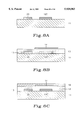
- FIG. 1 illustrates a prior art TFT display device which includes a protective etch-stop region and FIGS. 2A-2D illustrate a method of fabricating the device of FIG. 1.
- FIG. 1 illustrates a TFT display device comprising a gate electrode 2 on a substrate 1, a gate insulating region 3 on the gate electrode and a patterned amorphous silicon region 4 on the gate insulating region 3, opposite the gate electrode 2.
- a relatively highly doped amorphous silicon contact region 4 is also provided to facilitate the formation of low resistance contacts between source and drain electrodes 7 and 8 and the patterned amorphous silicon region 4.
- An etch stop 5 is also provided so that during a step of patterning the amorphous silicon contact region 4 into separate regions, the channel portion of the patterned amorphous silicon region 4 is not exposed to a chemical etchant.
- the TFT display device is also protected by a passivation layer 9.
- a conventional method of forming the TFT display device of FIG. 1 will now be described. As illustrated best by FIG. 2A, a gate electrode 2 is initially patterned on a face of a transparent substrate 1 and then a blanket electrically insulating layer 3 is deposited on the gate electrode 2. Then, a blanket amorphous silicon layer 40 and nitride layer 50 are formed in sequence on the electrically insulating layer 3 using such conventional techniques as plasma enhanced chemical vapor deposition (PECVD).
- PECVD plasma enhanced chemical vapor deposition
- a layer of photoresist (not shown) is then deposited on the nitride layer 50 and exposed by a light source which penetrates the substrate 1, but is selectively blocked by the patterned gate electrode 2.
- An etch stopper 5 is then formed by wet etching the nitride layer 50 using the layer of photoresist as a mask.
- a doped layer of amorphous silicon (e.g. N-type) is deposited on the etch stopper 5 and on the blanket amorphous silicon layer 40.
- the doped layer of amorphous silicon and blanket amorphous silicon layer 40 are then patterned using conventional techniques to define an amorphous silicon active region 4 having a doped amorphous silicon contact region 6 thereon.
- a blanket metal layer is then deposited and patterned using an etching technique to define source and drain electrodes 7 and 8.
- the doped amorphous silicon contact region 6 is also etched to form separate source and drain amorphous silicon contact regions.
- the etch stopper 5 is used as a mask to protect the amorphous silicon active region 4 from etching damage.
- a blanket passivation layer is formed on an upper surface of the TFT device.
- a method of forming a TFT display device containing liquid crystal display (LCD) cells therein includes the steps of forming a first conductive layer on a face of a substrate and then patterning the first conductive layer to define a plurality of parallel gate lines (with gate electrodes extending therefrom) and a plurality of parallel data lines which each comprise a plurality of data line segments.
- LCD liquid crystal display
- a first electrically insulating layer (e.g., SiO 2 , Si 3 N 4 ) is then formed on the data lines, the gate lines and the face of the substrate.
- a first undoped amorphous silicon (a-Si) layer is then formed on the first electrically insulating layer and patterned to define an amorphous silicon active region (for each cell) which extends opposite a respective gate electrode.
- a second electrically insulating layer is then formed as a passivation layer on the amorphous silicon active region and on the first electrically insulating layer.
- the first and second electrically insulating layers are then patterned to expose source and drain portions of the amorphous silicon active region and define at least one data line contact hole which exposes a portion of a data line segment for each cell.
- a second amorphous silicon layer of first conductivity type (e.g., N-type) is then formed on the exposed source and drain portions of the amorphous silicon active region and in the data line contact hole for each display cell.
- An optically transparent conductive layer e.g., indium-tin-oxide (ITO) is then formed on the second amorphous silicon layer.
- ITO indium-tin-oxide
- the optically transparent conductive layer and the doped second amorphous silicon layer are etched to define a source electrode (which electrically connects the data line to the source portion of the amorphous silicon active region) and define a pixel electrode (which is electrically connected to the drain portion of the amorphous silicon active region).
- a thin-film transistor (TFT) liquid crystal display (LCD) device which comprises a transparent substrate and a plurality of TFT-LCD cells having respective pixel electrodes.
- a gate line is also provided to interconnect the gate electrodes of a row of thin-film transistor display cells and a data line is provided to interconnect a column of thin-film transistor display cells.
- Each data line is comprised of a plurality of data line segments which are preferably spaced end-to-end as a string of data line segments.
- the data line(s) and gate line(s) are formed as coplanar lines by patterning the data line(s) and gate line(s) from the same conductive layer.
- a plurality of data line jumpers are also provided to electrically connect the data line segments in each data line together.
- These data line jumpers may be comprised of an optically transparent conductive material (e.g., ITO) and more preferably are comprised of a composite of an optically transparent conductive material and doped (e.g., N-type) amorphous silicon.
- FIG. 1 illustrates a schematic cross-sectional view of a conventional thin-film transistor (TFT) display device.
- TFT thin-film transistor
- FIGS. 2A-2D illustrate schematic cross-sectional views of intermediate structures illustrating a method of forming the thin-film transistor (TFT) display device of FIG. 1.
- TFT thin-film transistor
- FIG. 3 is a layout schematic of a thin-film transistor (TFT) display device according to a first embodiment of the present invention.
- TFT thin-film transistor
- FIG. 4 is a cross-sectional view of the display device of FIG. 3, taken along line IV-IV'.
- FIG. 5 is a cross-sectional view of the display device of FIG. 3, taken along line V-V'.
- FIGS. 6A-6C are intermediate layout schematic views illustrating a method of forming the display device of FIG. 3.
- FIGS. 7A-7E illustrate schematic cross-sectional views of intermediate structures illustrating a method of forming the display device of FIG. 3, taken along line VII-VII' in FIGS. 6A-6C.
- FIGS. 8A-8E illustrate schematic cross-sectional views of intermediate structures illustrating a method of forming the display device of FIG. 3, taken along line VIII-VIII' in FIGS. 6A-6C.
- FIG. 9 is a layout schematic of a thin-film transistor (TFT) display device according to a second embodiment of the present invention.
- TFT thin-film transistor
- FIG. 10 is a cross-sectional view of the display device of FIG. 9, taken along line X-X' in FIG. 9.
- FIG. 11 is a cross-sectional view of the display device of FIG. 9, taken along line XI-XI' in FIG. 9.
- FIG. 12 illustrates a schematic cross-sectional view of an intermediate structure illustrating a method of forming the display device of FIG. 9, taken along line X-X' in FIG. 9.
- FIG. 13 illustrates a schematic cross-sectional view of an intermediate structure illustrating a method of forming the display device of FIG. 9, taken along line XI-XI' in FIG. 9.
- a preferred display device comprises a two-dimensional array of TFT-LCD display cells.
- Each display cell is electrically coupled to a respective gate line 12 and a respective data line 20 which is comprised of a plurality of data line segments.
- These data line segments are coplanar with the gate lines 12 in the array, but are patterned to extend in orthogonal directions relative to the gate lines 12 so that an N ⁇ N matrix or grid of gate and data lines can be formed using the same level of metallization.
- each gate line 12 has a plurality of gate electrodes 120 extending from one side thereof in a direction parallel to the data lines 20.
- each gate line 12 Electrical contact to each gate line 12 is also made through a contact hole 1120 to a gate pad 1210.
- Each data line segment in a respective data line 20 is also electrically joined by a respective data line jumper.
- each data line jumper is contiguous with a respective source electrode 17.
- these data line jumpers are electrically connected through contact holes 121, 122 to respective data line segments.
- Electrical contact to each data line 20 is also made through a contact hole 1200 to a data pad 200.
- each display cell also comprises a patterned amorphous silicon active region 14 which extends opposite a respective gate electrode 120.
- Source and drain contact holes 141 and 142 are also formed in a passivation layer to expose source and drain portions of the amorphous silicon active region 14.
- a transparent conductive layer comprising indium-tin-oxide, for example, is also patterned to define a source electrode 17, which electrically connects the source portion of the amorphous silicon active region 14 to a data line segment (through a contact hole 121), and define a drain/pixel electrode 18 for each cell.
- FIGS. 4-5 cross-sectional views of the display device of FIG. 3, taken along lines IV-IV' and V-V', respectively, will be described.
- a data line jumper electrically connects opposing ends of adjacent data line segments 20 so that display data can be provided to each display cell in each column of cells, even though the data line segments 20 are patterned at the same level and from the same conductive layer as the gate lines 12.
- the data line jumpers preferably comprise a composite of an amorphous silicon layer 16 of first conductivity type (e.g., N-type) and a transparent conductive layer (e.g., indium-tin-oxide) which is patterned as a source electrode 17 and a pixel electrode 18.
- the gate line 12 and data line segments 20 are electrically insulated from each other on a substrate 11 (e.g., transparent substrate) by a first electrically insulating layer 13 (e.g., SiO 2 , Si 3 N 4 ).
- a second electrically insulating layer 19 e.g., passivation layer
- drain line contact holes are patterned in the first and second electrically insulating layers 13 and 19 to expose the ends of the data line segments 20, prior to formation of the data line jumpers.
- FIG. 5 a cross-sectional view of a preferred TFT display cell is illustrated.
- an end view of a data line segment 20 and a cross-sectional view of a gate electrode 120 are illustrated on the face of the substrate 11.
- the active region of the TFT i.e., source, channel and drain regions
- the active region of the TFT includes an amorphous silicon active region 14 which is formed on the first electrically insulating layer 13 and extends opposite the active region 14.
- a second electrically insulating layer 19 is also provided on the first electrically insulating layer 13.
- the second electrically insulating layer 19 is patterned to define an etch stopper region 15 and expose source and drain portions of the active region 14.
- the first and second electrically insulating layers 13 and 19 are also patterned to define data line contact holes which expose upper surfaces of the data line segments.
- a combined data line jumper/source electrode 17 and pixel electrode 18 are also provided by forming a doped amorphous silicon layer 16 on the patterned second electrically insulating layer 19 and then forming a transparent conductive layer on the doped amorphous silicon layer 16. These layers are then patterned to define separate electrodes 17 and 18.
- FIGS. 7A-7E and 8A-8E a preferred method of forming a display device according to a first embodiment of the present invention will be described.
- the cross-sectional views of FIGS. 7E and 8E correspond to the cross-sectional views of FIGS. 4 and 5, respectively.
- a first conductive layer e.g., metal
- FIGS. 7B and 8B a first electrically insulating layer 13 is then formed on the patterned first conductive layer.
- This first electrically insulating layer 13 may comprise silicon dioxide or silicon nitride. As illustrated by FIGS. 7C and 8C, an undoped layer of amorphous silicon (a-Si) is then deposited and patterned to define an amorphous silicon active region 14 which extends opposite the gate electrode 120 of the TFT. A second electrically insulating layer 19 such as a passivation layer is then deposited on the first electrically insulating layer 13 and on an upper surface of the amorphous silicon active region 14.
- a-Si amorphous silicon
- the first and second electrically insulating layers 13 and 19 are then patterned using conventional techniques to define data line contact holes 121 and 122 and expose spaced source (S) and drain (D) portions of the amorphous silicon active region 14 through contact holes 141 and 142.
- a doped layer e.g., N-type
- a transparent conductive layer e.g., indium-tin-oxide (ITO)
- ITO indium-tin-oxide
- FIGS. 6A-6C illustrate a layout schematic view of the structure of FIGS. 7A and 8A;
- FIG. 6B illustrates a layout schematic view of the structure of FIGS. 7B and 8B;
- FIG. 6C illustrates a layout schematic view of the structures of FIGS. 7E and 8E.
- FIG. 9 illustrates a layout schematic of a display device which is similar to the display device illustrated by FIG. 3, however, the drain line contact holes 1211 and 1221 and the source and drain contact holes 1410 and 1420 are formed in a different manner relative to the contact holes illustrated by FIG. 3.
- the drain line segments 20 and gate line 12 are patterned from a first conductive layer.
- a first electrically insulating layer and amorphous silicon layer are deposited in sequence on the gate electrode 120 and then patterned to define a gate insulating layer 13 and an amorphous silicon active region 14 on the gate insulating layer 13.
- the first electrically insulating layer is preferably removed from the data line segments 20 and gate line 12.
- a second electrically insulating layer 19 is deposited and patterned to expose the data line segments 20 through data line contact holes 1211 and 1221 and the face of the substrate 11 at source and drain contact holes 1410 and 1420.
- a doped layer e.g., N-type
- amorphous silicon 16 and a transparent conductive layer e.g., indium-tin-oxide (ITO)
- ITO indium-tin-oxide
- the channel portion (i.e., the TFT's channel region) of the amorphous silicon active region 14 is protected from this etching step by a central portion of the second electrically insulating layer 19 which acts as an etch stopper region 15.
Abstract
Description
Claims (3)
Applications Claiming Priority (2)
| Application Number | Priority Date | Filing Date | Title |
|---|---|---|---|
| KR1019960017223A KR100194679B1 (en) | 1996-05-21 | 1996-05-21 | Thin film transistor and fabrication method thereof |
| KR96-17223 | 1996-05-21 |
Publications (1)
| Publication Number | Publication Date |
|---|---|
| US5920083A true US5920083A (en) | 1999-07-06 |
Family
ID=19459348
Family Applications (1)
| Application Number | Title | Priority Date | Filing Date |
|---|---|---|---|
| US08/846,019 Expired - Lifetime US5920083A (en) | 1996-05-21 | 1997-04-25 | Thin-film transistor display devices having coplanar gate and drain lines |
Country Status (2)
| Country | Link |
|---|---|
| US (1) | US5920083A (en) |
| KR (1) | KR100194679B1 (en) |
Cited By (30)
| Publication number | Priority date | Publication date | Assignee | Title |
|---|---|---|---|---|
| US6256077B1 (en) | 1998-11-26 | 2001-07-03 | Samsung Electronics Co., Ltd. | Thin film transistor array panel for a liquid crystal display and a method for manufacturing the same using four photolithography steps |
| EP1128430A2 (en) * | 2000-02-22 | 2001-08-29 | Semiconductor Energy Laboratory Co., Ltd. | Semiconductor device and method of manufacturing the same |
| US20020044111A1 (en) * | 2000-05-12 | 2002-04-18 | Semiconductor Energy Laboratory Co., Ltd. | Light-emitting device and electric appliance |
| US6376288B1 (en) * | 2001-02-27 | 2002-04-23 | Hannstar Display Corp. | Method of forming thin film transistors for use in a liquid crystal display |
| US6466279B1 (en) * | 1998-04-23 | 2002-10-15 | Nec Corporation | Liquid crystal display device and process for producing same in which forming first and second organic insulating layers using curing and half curing process |
| US6633359B1 (en) * | 1999-08-05 | 2003-10-14 | Fujitsu Display Technologies Corporation | Liquid crystal display having signal lines on substrate intermittently extending and its manufacture |
| US6654091B2 (en) * | 2000-02-19 | 2003-11-25 | Lg. Philips Lcd Co., Ltd | Liquid crystal display device and its fabricating method in which the contact hole exposes gate insulating layer |
| US20040005739A1 (en) * | 2002-04-22 | 2004-01-08 | Masahiro Furusawa | Method of manufacturing device, device, and electronic apparatus |
| US20040004678A1 (en) * | 2002-04-22 | 2004-01-08 | Masahiro Furusawa | Method of manufacturing device, device, and electronic apparatus |
| US20040036816A1 (en) * | 2002-08-23 | 2004-02-26 | Lg.Philips Lcd Co., Ltd. | Liquid crystal display device and method for manufacturing the same |
| US6727559B2 (en) * | 2001-06-22 | 2004-04-27 | Sanyo Electric Co., Ltd. | Compound semiconductor device |
| US20040100434A1 (en) * | 2002-11-22 | 2004-05-27 | Lg.Philips Lcd Co., Ltd. | Wire structure of display device |
| DE10255626A1 (en) * | 2002-11-28 | 2004-06-17 | Infineon Technologies Ag | Method and device for arranging contacting elements of components of an integrated circuit, computer-readable storage medium and program element |
| US20040135520A1 (en) * | 2002-12-26 | 2004-07-15 | Lg.Philips Lcd Co., Ltd. | Organic electroluminescent device and manufacturing method for the same |
| EP1130566A3 (en) * | 2000-02-29 | 2008-06-11 | Sel Semiconductor Energy Laboratory Co., Ltd. | Display device and method for fabricating the same |
| US20090002611A1 (en) * | 2007-06-26 | 2009-01-01 | Shih-Chyuan Fan Jiang | Transflective liquid crystal display panel and pixel structure thereof |
| US20120256183A1 (en) * | 2011-04-07 | 2012-10-11 | Boe Technology Group Co., Ltd. | Thin film transistor array substrate, color filter substrate and display device |
| CN103178021A (en) * | 2013-02-28 | 2013-06-26 | 京东方科技集团股份有限公司 | Oxide thin-film transistor array substrate, manufacturing method for same and display panel |
| US8487315B2 (en) | 2000-04-12 | 2013-07-16 | Semiconductor Energy Laboratory Co., Ltd. | Illumination apparatus |
| CN103367248A (en) * | 2013-07-01 | 2013-10-23 | 京东方科技集团股份有限公司 | Array substrate, preparation method of array substrate and display device |
| US20130314633A1 (en) * | 2012-05-22 | 2013-11-28 | Electronics And Telecommunications Research Institute | Dual mode display apparatus and method of manufacturing the same |
| CN103474468A (en) * | 2013-07-12 | 2013-12-25 | 福建华映显示科技有限公司 | Oxide-semiconductor-film transistor |
| CN103489878A (en) * | 2013-10-09 | 2014-01-01 | 合肥京东方光电科技有限公司 | Array substrate, preparing method of array substrate and display device of array substrate |
| CN103985714A (en) * | 2013-12-31 | 2014-08-13 | 上海天马微电子有限公司 | Array substrate and manufacturing method thereof |
| US20140340607A1 (en) * | 2011-11-18 | 2014-11-20 | Sharp Kabushiki Kaisha | Semiconductor device, method for fabricating the semiconductor device and display device |
| CN104766819A (en) * | 2014-01-06 | 2015-07-08 | 瀚宇彩晶股份有限公司 | Pixel substrate and manufacture method thereof |
| US9093537B2 (en) | 2011-12-21 | 2015-07-28 | Lg Display Co., Ltd. | Display device and method for manufacturing the same |
| US9285631B2 (en) * | 2012-11-16 | 2016-03-15 | Boe Technology Group Co., Ltd. | Display device, transflective thin film transistor array substrate and manufacturing method thereof |
| CN105977266A (en) * | 2016-07-18 | 2016-09-28 | 深圳市华星光电技术有限公司 | TFT substrate and manufacturing method thereof |
| US20160322388A1 (en) * | 2015-04-28 | 2016-11-03 | Boe Technology Group Co., Ltd. | Array substrate, its manufacturing method and display device |
Families Citing this family (5)
| Publication number | Priority date | Publication date | Assignee | Title |
|---|---|---|---|---|
| KR100338480B1 (en) * | 1995-08-19 | 2003-01-24 | 엘지.필립스 엘시디 주식회사 | Liquid crystal display and method for fabricating the same |
| KR100390802B1 (en) * | 2001-05-24 | 2003-07-12 | 엘지.필립스 엘시디 주식회사 | Manufacturing method for tft-lcd |
| KR101604163B1 (en) | 2011-12-21 | 2016-03-17 | 엘지디스플레이 주식회사 | Display device and method for manufacturing of the same |
| KR101901251B1 (en) | 2011-12-27 | 2018-09-27 | 엘지디스플레이 주식회사 | Oxide semiconductor thin film transistor and method for manifacturing the same |
| KR101878926B1 (en) * | 2012-05-22 | 2018-07-16 | 한국전자통신연구원 | apparatus for displaying dual mode and manufacturing method of the same |
Citations (2)
| Publication number | Priority date | Publication date | Assignee | Title |
|---|---|---|---|---|
| US5604358A (en) * | 1995-01-20 | 1997-02-18 | Goldstar Co., Ltd. | Device of thin film transistor liquid crystal display |
| US5790222A (en) * | 1996-06-14 | 1998-08-04 | Lg Electronics Inc. | Thin film transistor array and method of manufacturing thereof |
-
1996
- 1996-05-21 KR KR1019960017223A patent/KR100194679B1/en not_active IP Right Cessation
-
1997
- 1997-04-25 US US08/846,019 patent/US5920083A/en not_active Expired - Lifetime
Patent Citations (2)
| Publication number | Priority date | Publication date | Assignee | Title |
|---|---|---|---|---|
| US5604358A (en) * | 1995-01-20 | 1997-02-18 | Goldstar Co., Ltd. | Device of thin film transistor liquid crystal display |
| US5790222A (en) * | 1996-06-14 | 1998-08-04 | Lg Electronics Inc. | Thin film transistor array and method of manufacturing thereof |
Cited By (63)
| Publication number | Priority date | Publication date | Assignee | Title |
|---|---|---|---|---|
| US20020191124A1 (en) * | 1998-04-23 | 2002-12-19 | Nec Corporation | Liquid crystal display device and process for producing same |
| US7321413B2 (en) | 1998-04-23 | 2008-01-22 | Nec Lcd Technologies, Ltd. | Liquid crystal display device and process for producing same |
| US6466279B1 (en) * | 1998-04-23 | 2002-10-15 | Nec Corporation | Liquid crystal display device and process for producing same in which forming first and second organic insulating layers using curing and half curing process |
| US6256077B1 (en) | 1998-11-26 | 2001-07-03 | Samsung Electronics Co., Ltd. | Thin film transistor array panel for a liquid crystal display and a method for manufacturing the same using four photolithography steps |
| US6633359B1 (en) * | 1999-08-05 | 2003-10-14 | Fujitsu Display Technologies Corporation | Liquid crystal display having signal lines on substrate intermittently extending and its manufacture |
| US6943859B2 (en) * | 2000-02-19 | 2005-09-13 | Lg.Philips Lcd Co., Ltd. | Liquid crystal display device and its fabricating method |
| US6654091B2 (en) * | 2000-02-19 | 2003-11-25 | Lg. Philips Lcd Co., Ltd | Liquid crystal display device and its fabricating method in which the contact hole exposes gate insulating layer |
| US8399884B2 (en) | 2000-02-22 | 2013-03-19 | Semiconductor Energy Laboratory Co., Ltd. | Semiconductor device and method of manufacturing the same |
| US20110169011A1 (en) * | 2000-02-22 | 2011-07-14 | Semiconductor Energy Laboratory Co., Ltd. | Semiconductor device and method of manufacturing the same |
| US9869907B2 (en) | 2000-02-22 | 2018-01-16 | Semiconductor Energy Laboratory Co., Ltd. | Semiconductor device and method of manufacturing the same |
| US20090267073A1 (en) * | 2000-02-22 | 2009-10-29 | Semiconductor Energy Laboratory Co., Ltd. | Semiconductor Device and Method of Manufacturing the Same |
| US8704233B2 (en) | 2000-02-22 | 2014-04-22 | Semiconductor Energy Laboratory Co., Ltd. | Semiconductor device and method of manufacturing the same |
| US9318610B2 (en) | 2000-02-22 | 2016-04-19 | Semiconductor Energy Laboratory Co., Ltd. | Semiconductor device and method of manufacturing the same |
| EP1128430A2 (en) * | 2000-02-22 | 2001-08-29 | Semiconductor Energy Laboratory Co., Ltd. | Semiconductor device and method of manufacturing the same |
| EP1128430A3 (en) * | 2000-02-22 | 2010-11-03 | Semiconductor Energy Laboratory Co., Ltd. | Semiconductor device and method of manufacturing the same |
| US7915615B2 (en) | 2000-02-22 | 2011-03-29 | Semiconductor Energy Laboratory Co., Ltd. | Semiconductor device and method of manufacturing the same |
| EP1130566A3 (en) * | 2000-02-29 | 2008-06-11 | Sel Semiconductor Energy Laboratory Co., Ltd. | Display device and method for fabricating the same |
| US9263476B2 (en) | 2000-02-29 | 2016-02-16 | Semiconductor Energy Laboratory Co., Ltd. | Display device and method for fabricating the same |
| US7612753B2 (en) | 2000-02-29 | 2009-11-03 | Semiconductor Energy Energy Laboratory Co., Ltd. | Display device and method for fabricating the same |
| US8344992B2 (en) | 2000-02-29 | 2013-01-01 | Semiconductor Energy Laboratory Co., Ltd. | Display device and method for fabricating the same |
| US8717262B2 (en) | 2000-02-29 | 2014-05-06 | Semiconductor Energy Laboratory Co., Ltd. | Display device and method for fabricating the same |
| US8829529B2 (en) | 2000-04-12 | 2014-09-09 | Semiconductor Energy Laboratory Co., Ltd. | Illumination apparatus |
| US8487315B2 (en) | 2000-04-12 | 2013-07-16 | Semiconductor Energy Laboratory Co., Ltd. | Illumination apparatus |
| US9704996B2 (en) | 2000-04-12 | 2017-07-11 | Semiconductor Energy Laboratory Co., Ltd. | Semiconductor device |
| US8669925B2 (en) | 2000-05-12 | 2014-03-11 | Semiconductor Energy Laboratory Co., Ltd. | Light-emitting device and electric appliance |
| US8284138B2 (en) | 2000-05-12 | 2012-10-09 | Semiconductor Energy Laboratory Co., Ltd. | Light-emitting device and electric appliance |
| US20020044111A1 (en) * | 2000-05-12 | 2002-04-18 | Semiconductor Energy Laboratory Co., Ltd. | Light-emitting device and electric appliance |
| US20100085283A1 (en) * | 2000-05-12 | 2010-04-08 | Semiconductor Energy Laboratory Co., Ltd. | Light-Emitting Device and Electric Appliance |
| US7633471B2 (en) | 2000-05-12 | 2009-12-15 | Semiconductor Energy Laboratory Co., Ltd. | Light-emitting device and electric appliance |
| US6376288B1 (en) * | 2001-02-27 | 2002-04-23 | Hannstar Display Corp. | Method of forming thin film transistors for use in a liquid crystal display |
| US6727559B2 (en) * | 2001-06-22 | 2004-04-27 | Sanyo Electric Co., Ltd. | Compound semiconductor device |
| US7208764B2 (en) * | 2002-04-22 | 2007-04-24 | Seiko Epson Corporation | Liquid crystal display device having partition walls |
| US7136127B2 (en) * | 2002-04-22 | 2006-11-14 | Seiko Epson Corporation | Method of manufacturing device, device, and electronic apparatus |
| US20040005739A1 (en) * | 2002-04-22 | 2004-01-08 | Masahiro Furusawa | Method of manufacturing device, device, and electronic apparatus |
| US20040004678A1 (en) * | 2002-04-22 | 2004-01-08 | Masahiro Furusawa | Method of manufacturing device, device, and electronic apparatus |
| US7167217B2 (en) * | 2002-08-23 | 2007-01-23 | Lg.Philips Lcd Co., Ltd. | Liquid crystal display device and method for manufacturing the same |
| US20040036816A1 (en) * | 2002-08-23 | 2004-02-26 | Lg.Philips Lcd Co., Ltd. | Liquid crystal display device and method for manufacturing the same |
| US7359022B2 (en) * | 2002-11-22 | 2008-04-15 | Lg.Philips Lcd Co., Ltd. | Wire structure of display device |
| US20040100434A1 (en) * | 2002-11-22 | 2004-05-27 | Lg.Philips Lcd Co., Ltd. | Wire structure of display device |
| DE10255626A1 (en) * | 2002-11-28 | 2004-06-17 | Infineon Technologies Ag | Method and device for arranging contacting elements of components of an integrated circuit, computer-readable storage medium and program element |
| US20040135520A1 (en) * | 2002-12-26 | 2004-07-15 | Lg.Philips Lcd Co., Ltd. | Organic electroluminescent device and manufacturing method for the same |
| US8071978B2 (en) * | 2002-12-26 | 2011-12-06 | Lg Display Co., Ltd. | Organic electroluminescent device comprising power supply line on same layer as gate line |
| US7692743B2 (en) * | 2007-06-26 | 2010-04-06 | Au Optronics Corp. | Transflective liquid crystal display panel and pixel structure thereof |
| US20090002611A1 (en) * | 2007-06-26 | 2009-01-01 | Shih-Chyuan Fan Jiang | Transflective liquid crystal display panel and pixel structure thereof |
| US20120256183A1 (en) * | 2011-04-07 | 2012-10-11 | Boe Technology Group Co., Ltd. | Thin film transistor array substrate, color filter substrate and display device |
| US8907342B2 (en) * | 2011-04-07 | 2014-12-09 | Boe Technology Group Co., Ltd. | Thin film transistor array substrate, color filter substrate and display device |
| US20140340607A1 (en) * | 2011-11-18 | 2014-11-20 | Sharp Kabushiki Kaisha | Semiconductor device, method for fabricating the semiconductor device and display device |
| US9093537B2 (en) | 2011-12-21 | 2015-07-28 | Lg Display Co., Ltd. | Display device and method for manufacturing the same |
| CN103178082B (en) * | 2011-12-21 | 2016-03-16 | 乐金显示有限公司 | Display device and manufacture method thereof |
| US20130314633A1 (en) * | 2012-05-22 | 2013-11-28 | Electronics And Telecommunications Research Institute | Dual mode display apparatus and method of manufacturing the same |
| US9379350B2 (en) * | 2012-05-22 | 2016-06-28 | Electronics And Telecommunications Research Institute | Dual mode display apparatus and method of manufacturing the same |
| US9285631B2 (en) * | 2012-11-16 | 2016-03-15 | Boe Technology Group Co., Ltd. | Display device, transflective thin film transistor array substrate and manufacturing method thereof |
| CN103178021A (en) * | 2013-02-28 | 2013-06-26 | 京东方科技集团股份有限公司 | Oxide thin-film transistor array substrate, manufacturing method for same and display panel |
| US9190432B2 (en) | 2013-02-28 | 2015-11-17 | Boe Technology Group Co., Ltd | Oxide thin-film transistor array substrate, manufacturing method thereof and display panel |
| CN103367248A (en) * | 2013-07-01 | 2013-10-23 | 京东方科技集团股份有限公司 | Array substrate, preparation method of array substrate and display device |
| CN103474468A (en) * | 2013-07-12 | 2013-12-25 | 福建华映显示科技有限公司 | Oxide-semiconductor-film transistor |
| CN103489878A (en) * | 2013-10-09 | 2014-01-01 | 合肥京东方光电科技有限公司 | Array substrate, preparing method of array substrate and display device of array substrate |
| CN103985714A (en) * | 2013-12-31 | 2014-08-13 | 上海天马微电子有限公司 | Array substrate and manufacturing method thereof |
| CN103985714B (en) * | 2013-12-31 | 2017-02-01 | 上海天马微电子有限公司 | Array substrate and manufacturing method thereof |
| CN104766819A (en) * | 2014-01-06 | 2015-07-08 | 瀚宇彩晶股份有限公司 | Pixel substrate and manufacture method thereof |
| CN104766819B (en) * | 2014-01-06 | 2017-12-08 | 瀚宇彩晶股份有限公司 | Picture element substrate and its manufacture method |
| US20160322388A1 (en) * | 2015-04-28 | 2016-11-03 | Boe Technology Group Co., Ltd. | Array substrate, its manufacturing method and display device |
| CN105977266A (en) * | 2016-07-18 | 2016-09-28 | 深圳市华星光电技术有限公司 | TFT substrate and manufacturing method thereof |
Also Published As
| Publication number | Publication date |
|---|---|
| KR970077744A (en) | 1997-12-12 |
| KR100194679B1 (en) | 1999-07-01 |
Similar Documents
| Publication | Publication Date | Title |
|---|---|---|
| US5920083A (en) | Thin-film transistor display devices having coplanar gate and drain lines | |
| US6878966B2 (en) | Thin-film transistor display devices | |
| US6028653A (en) | Active matrix liquid crystal display panel having an improved numerical aperture and display reliability and wiring designing method therefor | |
| US5828433A (en) | Liquid crystal display device and a method of manufacturing the same | |
| JP4733005B2 (en) | Array substrate for liquid crystal display device using organic semiconductor material and method for manufacturing the same | |
| US5917564A (en) | Methods of forming active matrix display devices with reduced susceptibility to image-sticking and devices formed thereby | |
| KR20040024666A (en) | Liquid crystal display and method of manufacturing the same | |
| JPH04163528A (en) | Active matrix display | |
| KR100673331B1 (en) | Liquid crystal display and method for fabricating the same | |
| US7924355B2 (en) | Liquid crystal display device | |
| JPH028821A (en) | Active matrix substrate | |
| KR20030056537A (en) | Method for manufacturing liquid crystal display device | |
| KR19990030877A (en) | Thin film transistor substrate and manufacturing method for liquid crystal display | |
| KR100205867B1 (en) | Active matrix substrate and its fabrication method | |
| JP3308100B2 (en) | TFT type liquid crystal display | |
| KR100514764B1 (en) | Liquid crystal display device and the method for manufaturing the same | |
| KR0139348B1 (en) | Manufacturing method of liquid crystal display panel | |
| KR100192886B1 (en) | Fabrication method of liquid crystal display device | |
| KR100397672B1 (en) | an array panel for liquid crystal display and manufacturing method thereof | |
| KR20070121992A (en) | Array substrate for liquid crystal display device and method of fabricating the same | |
| JPH04264527A (en) | Active matrix substrate | |
| JP2001330854A (en) | Liquid crystal display device | |
| KR100315922B1 (en) | Manufacturing method of thin film transistor substrate for liquid crystal display device using four masks and thin film transistor substrate for liquid crystal display device | |
| KR101250317B1 (en) | Array substrate for liquid crystal display device and the method of fabricating the same | |
| KR19990056727A (en) | LCD and its manufacturing method |
Legal Events
| Date | Code | Title | Description |
|---|---|---|---|
| AS | Assignment |
Owner name: SAMSUNG ELECTRONICS CO., LTD., KOREA, REPUBLIC OF Free format text: ASSIGNMENT OF ASSIGNORS INTEREST;ASSIGNOR:BAE, BYUNG-SEONG;REEL/FRAME:008722/0192 Effective date: 19970418 |
|
| FEPP | Fee payment procedure |
Free format text: PAYOR NUMBER ASSIGNED (ORIGINAL EVENT CODE: ASPN); ENTITY STATUS OF PATENT OWNER: LARGE ENTITY |
|
| STCF | Information on status: patent grant |
Free format text: PATENTED CASE |
|
| FPAY | Fee payment |
Year of fee payment: 4 |
|
| FPAY | Fee payment |
Year of fee payment: 8 |
|
| FEPP | Fee payment procedure |
Free format text: PAYER NUMBER DE-ASSIGNED (ORIGINAL EVENT CODE: RMPN); ENTITY STATUS OF PATENT OWNER: LARGE ENTITY |
|
| FEPP | Fee payment procedure |
Free format text: PAYOR NUMBER ASSIGNED (ORIGINAL EVENT CODE: ASPN); ENTITY STATUS OF PATENT OWNER: LARGE ENTITY |
|
| FPAY | Fee payment |
Year of fee payment: 12 |
|
| AS | Assignment |
Owner name: SAMSUNG DISPLAY CO., LTD., KOREA, REPUBLIC OF Free format text: CHANGE OF NAME;ASSIGNOR:SAMSUNG ELECTRONICS CO., LTD.;REEL/FRAME:028860/0244 Effective date: 20120403 |