US5990701A - Method of broadly distributing termination for buses using switched terminators - Google Patents
Method of broadly distributing termination for buses using switched terminators Download PDFInfo
- Publication number
- US5990701A US5990701A US08/881,927 US88192797A US5990701A US 5990701 A US5990701 A US 5990701A US 88192797 A US88192797 A US 88192797A US 5990701 A US5990701 A US 5990701A
- Authority
- US
- United States
- Prior art keywords
- pull
- line
- circuit
- signal
- resistance
- Prior art date
- Legal status (The legal status is an assumption and is not a legal conclusion. Google has not performed a legal analysis and makes no representation as to the accuracy of the status listed.)
- Expired - Lifetime
Links
Images


Classifications
-
- G—PHYSICS
- G06—COMPUTING; CALCULATING OR COUNTING
- G06F—ELECTRIC DIGITAL DATA PROCESSING
- G06F13/00—Interconnection of, or transfer of information or other signals between, memories, input/output devices or central processing units
- G06F13/38—Information transfer, e.g. on bus
- G06F13/40—Bus structure
- G06F13/4063—Device-to-bus coupling
- G06F13/4068—Electrical coupling
- G06F13/4086—Bus impedance matching, e.g. termination
Definitions
- the present invention relates to buses and more particularly to termination of buses for use in information processing systems.
- the signal frequency at which this communication occurs can limit the performance of the overall system. Thus, the higher the communication frequency, the better.
- the maximum frequency at which a system communicates is a function not only of the time that it takes for the electromagnetic wavefronts to propagate on the bus from one chip to another, but also of the time required for the signals to settle to levels than can be recognized reliably at the receiving bus nodes as being high or low, referred to as the settling time.
- the length of the settling time is a function of the amount of reflection and ringing that occurs on the signal bus. The more effective the termination of a bus system, the smaller the effects of reflection and ringing in the system and the shorter the overall settling time of the signal.
- a bus may be provided with broadly distributed signal termination by using switched termination logic where the pull up resistance of the driver corresponds to the characteristic impedance of the line and the pull down resistance of the driver corresponds to the number of drivers coupled to the line. Accordingly, signals being transmitted over the bus suffer relatively few reflections thus advantageously producing a shortened signal settling time, thereby increasing the attainable signaling frequency.
- the invention relates to a method for terminating a line having a number of drivers coupled thereto, the line having a characteristic impedance.
- the method includes the steps of pulling up a signal on the line with a pull up resistance substantially corresponding to the characteristic impedance of the line; and pulling down a signal on the line with a pull down resistance substantially corresponding to the number of drivers coupled to the line.
- the invention relates to a method for terminating a line having a plurality of ends, the line having a characteristic impedance.
- the method includes the steps of coupling a plurality of drivers to the plurality of ends, each driver including a pull up circuit, and a pull down circuit, the plurality of drivers being divided into a driving driver and a plurality of receiving drivers, pulling up a signal on the line with the pull up circuit of the driving driver, the pull up circuit of the driving driver having a pull up resistance corresponding to the impedance of the line, the receiving drivers having a resistance corresponding to the impedance of the line when the driving driver is pulling up the signal; pulling down a signal on the line with the pull down circuit of the driving driver, the pull down circuit having a pull down resistance corresponding to the number of drivers coupled to the line, the receiving drivers having a resistance corresponding to the impedance of the line when the driving driver is pulling down the signal.
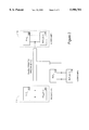
- FIG. 1 shows a block diagram of an information handling system having a bus as well as driver circuits in accordance with the present invention.
- FIG. 2 shows a block diagram of broadly distributed termination using switched termination logic of the information handling system of FIG. 1.
- FIGS. 3A, 3B, 3C and 3D show schematic block diagrams of a variety of bit elements of the driver circuits having switched termination logic in accordance with the present invention.
- information handling system 100 includes a plurality of components 102 such as processor 102a, memory controller 102b, and I/O controller 102c. It will be appreciated that these components 102 may be any type of component commonly found in an information handling system. Each of these components 102 is generally configured as an individual integrated circuit chip. However, it is known to combine various components into a single integrated circuit chip. Components 102 are coupled via bus 104. Bus 104 includes a plurality of parallel lines which are coupled to individual signal outputs of each of the components 102. Components 102 are also coupled to a common reference voltage (REF)
- REF common reference voltage
- Each component 102 includes a plurality of input/output circuits 108 which are coupled to individual signal paths of bus 104.
- Each input/output circuit 108 includes a receiver circuit 109 and a driver circuit 110.
- Each receiver circuit 109 is also coupled to the common reference voltage.
- Component 102 also includes impedance control circuit 112 which is coupled to each driver circuit 110. Impedance control circuit 112 controls driver circuits 110 so that the impedance of each pull up driver circuit is matched to that of the bus 104 and the impedance of each pull down driver circuit is equal to the impedance of the bus 104 divided by the difference of the number of drivers coupled to the bus minus one.
- driver circuits 110 include switchable termination logic for controlling whether each driver circuit 110 is driving or terminating and thus each driver circuit includes circuitry which controls the pull up and pull down termination resistance of the driver circuit.
- each driver circuit 110 of information handling system 100 includes a plurality of signal nodes coupled to bus 104 having a characteristic impedance of Z O . Attached to each signal node at the end of a transmission line trace or stub is a the push-pull driver 110.
- Driver 110 includes a pull up driver circuit 202 and a pull down driver circuit 204.
- Pull up driver circuit 202 includes a pull up resistance that is substantially equal to (i.e., within 5% of) the characteristic impedance Z O of the transmission line.
- Pull down driver circuit 204 includes a pull down resistance that is substantially equal to(i.e., within 5% of) ##EQU1## where n is the number of nodes in the information handling system 100.
- the receiver if any, functions as a small capacitive load; however, no DC current flows between the receiver and the transmission line. Accordingly, the receiver does not contribute to the output impedance of the driver.
- the driver 110 of the node When a node is driving signals onto line 104, the driver 110 of the node either pulls the signal up or pulls the signal down, as appropriate to send the desired digital signal. When a node is receiving, the pull up portion of the driver remains active continuously, thereby functioning as a terminating resistance which is matched to the impedance of the transmission line.
- the signal swing on the bus 104 is from VDD to VDD/2. Accordingly, the receivers are capable of resolving a swing of VDD/2.
- the impedance at each receiving node is matched to the impedance of the transmission line, signals arriving at the receiving node terminate without reflection.
- the impedance at the driving node is also matched to the line when driving high.
- the impedance at the driving node is mismatched when driving the signal low because the impedance is equal to Z O /(n-1) instead of Z O .
- the only stub on which reflections are created is the stub with the driver when the driver pulls the signal low.
- there is an impedance mismatch at the intersection of this stub with the rest of the bus only a fraction of these reflections, which fraction is already a fraction of the initial signal, are transmitted to the receiving nodes. This condition is preferable because the settling time of the receiving node is the crucial parameter to bus performance. The net effect of the absence of reflections from the stub ends can be a reduced overall settling time when compared to systems without termination at each receiving node.
- the pull down resistance is Z O /(n-1) because, by having the pull up resistors on chip, the pull up resistance at the driving node is switched off when the driver is pulling low. Accordingly, this system advantageously consumes less overall current and power than a system that has an off chip pull up resistor that is always drawing current.
- each component 102 improves signal integrity when compared to having a termination resistor that is not within component 102.
- the terminator is actually separated from the receiving node by some distance along a transmission line and thus parasitics are introduced in the connection to the termination resistor. Also, because of the separation such a system can have reflections from the intersection of the stubs of the transmission line. However, when the termination is within each component, the termination resistance is placed right at the receiver, thereby reducing reflections and ringing.
- the pull up and pull down elements of driver circuit 110 may be of a variety of configurations.
- the driver element may be a PMOS transistor.
- the driver element may be the parallel combination of a PMOS transistor and an NMOS transistor. With this parallel combination, it is the resistance of the parallel combination that would be equal to the desired bit element resistance.
- the driver element may be an NMOS transistor.
- the driver element may be the parallel combination of two NMOS transistors.
- the pull up driver element includes the parallel combination of the PMOS transistor and the NMOS transistor and the pull down element includes the parallel combination of two NMOS transistors. It will be appreciated that a driver circuit may have other circuitry that contributes to the overall pull up and pull down resistance of the driver.
- driver configurations are disclosed for the pull up and pull down driver elements, it will be appreciated that other driver configurations may be used so long as the appropriate driver and termination resistances are maintained.
- a MOS transistor may be conceptualized as having a control terminal which controls the flow of current between a first current handling terminal and a second current handling terminal.
- MOS transistors are frequently discussed as having a drain, a gate, and a source, in most such devices the drain is interchangeable with the source. This is because the layout and semiconductor processing of the transistor is symmetrical (which is typically not the case for bipolar transistors).
- the current handling terminal normally residing at the higher voltage is customarily called the drain.
- the current handling terminal normally residing at the lower voltage is customarily called the source. A sufficient voltage on the gate causes a current to therefore flow from the drain to the source.
- the gate to source voltage referred to in an N-channel MOS device equations merely refers to whichever diffusion (drain or source) has the lower voltage at any given time.
- the "source" of an N-channel device of a bi-directional CMOS transfer gate depends on which side of the transfer gate is at a lower voltage.
- the control terminal is the gate
- the first current handling terminal may be termed the "drain/source”
- the second current handling terminal may be termed the "source/drain”.
- a description is equally valid for a P channel MOS transistor, since the polarity between drain and source voltages, and the direction of current flow between drain and source, is not implied by such terminology.
- one current handling terminal may be arbitrarily deemed the "drain” and the other deemed the "source”, with an implicit understanding that the two are not distinct, but interchangeable.
Abstract
Description
Claims (12)
Priority Applications (4)
| Application Number | Priority Date | Filing Date | Title |
|---|---|---|---|
| US08/881,927 US5990701A (en) | 1997-06-25 | 1997-06-25 | Method of broadly distributing termination for buses using switched terminators |
| US09/315,325 US6323672B1 (en) | 1997-06-25 | 1999-05-19 | Apparatus for reducing reflections when using dynamic termination logic signaling |
| US09/315,326 US6323673B1 (en) | 1997-06-25 | 1999-05-19 | Apparatus for dynamic termination logic signaling |
| US09/318,544 US6275062B1 (en) | 1997-06-25 | 1999-05-25 | Termination of transmission lines using simultaneously enabled pull-up and pull-down circuits |
Applications Claiming Priority (1)
| Application Number | Priority Date | Filing Date | Title |
|---|---|---|---|
| US08/881,927 US5990701A (en) | 1997-06-25 | 1997-06-25 | Method of broadly distributing termination for buses using switched terminators |
Related Child Applications (3)
| Application Number | Title | Priority Date | Filing Date |
|---|---|---|---|
| US09/315,326 Continuation-In-Part US6323673B1 (en) | 1997-06-25 | 1999-05-19 | Apparatus for dynamic termination logic signaling |
| US09/315,325 Continuation-In-Part US6323672B1 (en) | 1997-06-25 | 1999-05-19 | Apparatus for reducing reflections when using dynamic termination logic signaling |
| US09/318,544 Continuation US6275062B1 (en) | 1997-06-25 | 1999-05-25 | Termination of transmission lines using simultaneously enabled pull-up and pull-down circuits |
Publications (1)
| Publication Number | Publication Date |
|---|---|
| US5990701A true US5990701A (en) | 1999-11-23 |
Family
ID=25379502
Family Applications (2)
| Application Number | Title | Priority Date | Filing Date |
|---|---|---|---|
| US08/881,927 Expired - Lifetime US5990701A (en) | 1997-06-25 | 1997-06-25 | Method of broadly distributing termination for buses using switched terminators |
| US09/318,544 Expired - Fee Related US6275062B1 (en) | 1997-06-25 | 1999-05-25 | Termination of transmission lines using simultaneously enabled pull-up and pull-down circuits |
Family Applications After (1)
| Application Number | Title | Priority Date | Filing Date |
|---|---|---|---|
| US09/318,544 Expired - Fee Related US6275062B1 (en) | 1997-06-25 | 1999-05-25 | Termination of transmission lines using simultaneously enabled pull-up and pull-down circuits |
Country Status (1)
| Country | Link |
|---|---|
| US (2) | US5990701A (en) |
Cited By (11)
| Publication number | Priority date | Publication date | Assignee | Title |
|---|---|---|---|---|
| US6177807B1 (en) * | 1999-05-28 | 2001-01-23 | International Business Machines Corporation | High frequency valid data strobe |
| US6219812B1 (en) * | 1998-06-11 | 2001-04-17 | Sun Microsystems, Inc. | Apparatus and method for interfacing boundary-scan circuitry with DTL output drivers |
| US6232792B1 (en) | 1997-06-25 | 2001-05-15 | Sun Microsystems, Inc. | Terminating transmission lines using on-chip terminator circuitry |
| US6275062B1 (en) * | 1997-06-25 | 2001-08-14 | Sun Microsystems, Inc. | Termination of transmission lines using simultaneously enabled pull-up and pull-down circuits |
| US6285215B1 (en) * | 1999-09-02 | 2001-09-04 | Micron Technology, Inc. | Output driver having a programmable edge rate |
| US6300789B1 (en) * | 1999-12-22 | 2001-10-09 | Intel Corporation | Dynamic termination for non-symmetric transmission line network topologies |
| US6323672B1 (en) | 1997-06-25 | 2001-11-27 | Sun Microsystems, Inc. | Apparatus for reducing reflections when using dynamic termination logic signaling |
| US6323673B1 (en) * | 1997-06-25 | 2001-11-27 | Sun Microsystems, Inc. | Apparatus for dynamic termination logic signaling |
| US6484293B1 (en) * | 2000-07-14 | 2002-11-19 | Sun Microsystems, Inc. | Method for determining optimal configuration for multinode bus |
| US20030190849A1 (en) * | 2002-04-05 | 2003-10-09 | Deas Alexander Roger | Line termination incorporating compensation for device and package parasitics |
| US20090094601A1 (en) * | 2006-04-27 | 2009-04-09 | Vstovskiy Vladimir Nikitich | Method and device for protecting software from unauthorized use |
Families Citing this family (7)
| Publication number | Priority date | Publication date | Assignee | Title |
|---|---|---|---|---|
| KR100468467B1 (en) | 2002-01-12 | 2005-01-27 | 삼성전자주식회사 | Receive line defective wiring checking apparatus |
| US7199681B2 (en) * | 2002-04-19 | 2007-04-03 | Intel Corporation | Interconnecting of digital devices |
| US6847225B2 (en) * | 2003-03-21 | 2005-01-25 | Infineon Technologies Ag | CML (current mode logic) OCD (off chip driver)—ODT (on die termination) circuit for bidirectional data transmission |
| TW200910373A (en) | 2007-06-08 | 2009-03-01 | Mosaid Technologies Inc | Dynamic impedance control for input/output buffers |
| KR101139630B1 (en) * | 2010-12-09 | 2012-05-30 | 한양대학교 산학협력단 | Apparatus and method for generating identification key |
| KR101118826B1 (en) | 2011-02-15 | 2012-04-20 | 한양대학교 산학협력단 | Encryption apparatus and method for preventing physical attack |
| KR102186475B1 (en) | 2013-12-31 | 2020-12-03 | 주식회사 아이씨티케이 홀딩스 | Apparatus and method for generating random digital value |
Citations (24)
| Publication number | Priority date | Publication date | Assignee | Title |
|---|---|---|---|---|
| US4694205A (en) * | 1985-06-03 | 1987-09-15 | Advanced Micro Devices, Inc. | Midpoint sense amplification scheme for a CMOS DRAM |
| US4707620A (en) * | 1986-07-22 | 1987-11-17 | Tektronix, Inc. | Adjustable impedance driver network |
| US4719369A (en) * | 1985-08-14 | 1988-01-12 | Hitachi, Ltd. | Output circuit having transistor monitor for matching output impedance to load impedance |
| US4743784A (en) * | 1985-07-08 | 1988-05-10 | Nec Corporation | Sense amplifier circuit |
| US4804871A (en) * | 1987-07-28 | 1989-02-14 | Advanced Micro Devices, Inc. | Bit-line isolated, CMOS sense amplifier |
| US4831287A (en) * | 1988-04-11 | 1989-05-16 | Motorola, Inc. | Latching sense amplifier |
| US4845675A (en) * | 1988-01-22 | 1989-07-04 | Texas Instruments Incorporated | High-speed data latch with zero data hold time |
| US4855628A (en) * | 1986-11-21 | 1989-08-08 | Samsung Semiconductors And Telecommunications Co., Ltd. | Sense amplifier for high performance dram |
| US4859877A (en) * | 1988-01-04 | 1989-08-22 | Gte Laboratories Incorporated | Bidirectional digital signal transmission system |
| US4931675A (en) * | 1986-03-05 | 1990-06-05 | Kabushiki Kaisha Toshiba | Semiconductor sense amplifier |
| US4937479A (en) * | 1988-01-30 | 1990-06-26 | Nec Corporation | Data latch circuit with improved data write control function |
| US4959563A (en) * | 1988-06-29 | 1990-09-25 | Texas Instruments Incorporated | Adjustable low noise output circuit |
| JPH04178995A (en) * | 1990-11-14 | 1992-06-25 | Sharp Corp | Semiconductor storage device |
| US5134311A (en) * | 1990-06-07 | 1992-07-28 | International Business Machines Corporation | Self-adjusting impedance matching driver |
| US5162672A (en) * | 1990-12-24 | 1992-11-10 | Motorola, Inc. | Data processor having an output terminal with selectable output impedances |
| US5194765A (en) * | 1991-06-28 | 1993-03-16 | At&T Bell Laboratories | Digitally controlled element sizing |
| US5371420A (en) * | 1992-03-30 | 1994-12-06 | Mitsubishi Denki Kabushiki Kaisha | Output circuit having reduced switching noise |
| US5457407A (en) * | 1994-07-06 | 1995-10-10 | Sony Electronics Inc. | Binary weighted reference circuit for a variable impedance output buffer |
| US5602494A (en) * | 1995-03-09 | 1997-02-11 | Honeywell Inc. | Bi-directional programmable I/O cell |
| US5615161A (en) * | 1996-02-22 | 1997-03-25 | Hal Computer Systems, Inc. | Clocked sense amplifier with positive source feedback |
| US5644252A (en) * | 1995-03-09 | 1997-07-01 | Nec Corporation | Driver for interfacing integrated circuits to transmission lines |
| US5666078A (en) * | 1996-02-07 | 1997-09-09 | International Business Machines Corporation | Programmable impedance output driver |
| US5726583A (en) * | 1996-07-19 | 1998-03-10 | Kaplinsky; Cecil H. | Programmable dynamic line-termination circuit |
| US5852579A (en) * | 1997-06-19 | 1998-12-22 | Cypress Semiconductor Corporation | Method and circuit for preventing and/or inhibiting contention in a system employing a random access memory |
Family Cites Families (20)
| Publication number | Priority date | Publication date | Assignee | Title |
|---|---|---|---|---|
| JPH01502625A (en) * | 1987-05-01 | 1989-09-07 | ディジタル イクイプメント コーポレーション | Node for backplane bus |
| US5274671A (en) * | 1991-08-14 | 1993-12-28 | Hewlett Packard Company | Use of output impedance control to eliminate mastership change-over delays in a data communication network |
| JPH0685653A (en) | 1992-05-06 | 1994-03-25 | Sgs Thomson Microelectron Inc | Receiver circuit provided with bus keeper feature |
| US5347177A (en) * | 1993-01-14 | 1994-09-13 | Lipp Robert J | System for interconnecting VLSI circuits with transmission line characteristics |
| US5463326A (en) | 1993-04-13 | 1995-10-31 | Hewlett-Packard Company | Output drivers in high frequency circuits |
| US5686872A (en) | 1995-03-13 | 1997-11-11 | National Semiconductor Corporation | Termination circuit for computer parallel data port |
| US5528168A (en) * | 1995-03-29 | 1996-06-18 | Intel Corporation | Power saving terminated bus |
| US5530377A (en) | 1995-07-05 | 1996-06-25 | International Business Machines Corporation | Method and apparatus for active termination of a line driver/receiver |
| US5592104A (en) | 1995-12-13 | 1997-01-07 | Lsi Logic Corporation | Output buffer having transmission gate and isolated supply terminals |
| US6026456A (en) | 1995-12-15 | 2000-02-15 | Intel Corporation | System utilizing distributed on-chip termination |
| US5705937A (en) | 1996-02-23 | 1998-01-06 | Cypress Semiconductor Corporation | Apparatus for programmable dynamic termination |
| US5731711A (en) | 1996-06-26 | 1998-03-24 | Lucent Technologies Inc. | Integrated circuit chip with adaptive input-output port |
| US6060907A (en) * | 1997-06-25 | 2000-05-09 | Sun Microsystems, Inc. | Impedance control circuit |
| US5955894A (en) * | 1997-06-25 | 1999-09-21 | Sun Microsystems, Inc. | Method for controlling the impedance of a driver circuit |
| US5982191A (en) * | 1997-06-25 | 1999-11-09 | Sun Microsystems, Inc. | Broadly distributed termination for buses using switched terminator logic |
| US5990701A (en) * | 1997-06-25 | 1999-11-23 | Sun Microsystems, Inc. | Method of broadly distributing termination for buses using switched terminators |
| JPH1145138A (en) * | 1997-07-25 | 1999-02-16 | Mitsubishi Electric Corp | High-speed bus circuit system |
| US6084424A (en) | 1997-12-30 | 2000-07-04 | Lsi Logic Corporation | Adjustable biasing voltage for a bus line and associated method |
| US6054881A (en) * | 1998-01-09 | 2000-04-25 | Advanced Micro Devices, Inc. | Input/output (I/O) buffer selectively providing resistive termination for a transmission line coupled thereto |
| US6087853A (en) | 1998-06-22 | 2000-07-11 | Lucent Technologies, Inc. | Controlled output impedance buffer using CMOS technology |
-
1997
- 1997-06-25 US US08/881,927 patent/US5990701A/en not_active Expired - Lifetime
-
1999
- 1999-05-25 US US09/318,544 patent/US6275062B1/en not_active Expired - Fee Related
Patent Citations (25)
| Publication number | Priority date | Publication date | Assignee | Title |
|---|---|---|---|---|
| US4694205A (en) * | 1985-06-03 | 1987-09-15 | Advanced Micro Devices, Inc. | Midpoint sense amplification scheme for a CMOS DRAM |
| US4743784A (en) * | 1985-07-08 | 1988-05-10 | Nec Corporation | Sense amplifier circuit |
| US4719369A (en) * | 1985-08-14 | 1988-01-12 | Hitachi, Ltd. | Output circuit having transistor monitor for matching output impedance to load impedance |
| US4931675A (en) * | 1986-03-05 | 1990-06-05 | Kabushiki Kaisha Toshiba | Semiconductor sense amplifier |
| US4707620A (en) * | 1986-07-22 | 1987-11-17 | Tektronix, Inc. | Adjustable impedance driver network |
| US4855628A (en) * | 1986-11-21 | 1989-08-08 | Samsung Semiconductors And Telecommunications Co., Ltd. | Sense amplifier for high performance dram |
| US4804871A (en) * | 1987-07-28 | 1989-02-14 | Advanced Micro Devices, Inc. | Bit-line isolated, CMOS sense amplifier |
| US4859877A (en) * | 1988-01-04 | 1989-08-22 | Gte Laboratories Incorporated | Bidirectional digital signal transmission system |
| US4845675A (en) * | 1988-01-22 | 1989-07-04 | Texas Instruments Incorporated | High-speed data latch with zero data hold time |
| US4937479A (en) * | 1988-01-30 | 1990-06-26 | Nec Corporation | Data latch circuit with improved data write control function |
| US4937479B1 (en) * | 1988-01-30 | 1992-07-21 | Nippon Electric Co | |
| US4831287A (en) * | 1988-04-11 | 1989-05-16 | Motorola, Inc. | Latching sense amplifier |
| US4959563A (en) * | 1988-06-29 | 1990-09-25 | Texas Instruments Incorporated | Adjustable low noise output circuit |
| US5134311A (en) * | 1990-06-07 | 1992-07-28 | International Business Machines Corporation | Self-adjusting impedance matching driver |
| JPH04178995A (en) * | 1990-11-14 | 1992-06-25 | Sharp Corp | Semiconductor storage device |
| US5162672A (en) * | 1990-12-24 | 1992-11-10 | Motorola, Inc. | Data processor having an output terminal with selectable output impedances |
| US5194765A (en) * | 1991-06-28 | 1993-03-16 | At&T Bell Laboratories | Digitally controlled element sizing |
| US5371420A (en) * | 1992-03-30 | 1994-12-06 | Mitsubishi Denki Kabushiki Kaisha | Output circuit having reduced switching noise |
| US5457407A (en) * | 1994-07-06 | 1995-10-10 | Sony Electronics Inc. | Binary weighted reference circuit for a variable impedance output buffer |
| US5602494A (en) * | 1995-03-09 | 1997-02-11 | Honeywell Inc. | Bi-directional programmable I/O cell |
| US5644252A (en) * | 1995-03-09 | 1997-07-01 | Nec Corporation | Driver for interfacing integrated circuits to transmission lines |
| US5666078A (en) * | 1996-02-07 | 1997-09-09 | International Business Machines Corporation | Programmable impedance output driver |
| US5615161A (en) * | 1996-02-22 | 1997-03-25 | Hal Computer Systems, Inc. | Clocked sense amplifier with positive source feedback |
| US5726583A (en) * | 1996-07-19 | 1998-03-10 | Kaplinsky; Cecil H. | Programmable dynamic line-termination circuit |
| US5852579A (en) * | 1997-06-19 | 1998-12-22 | Cypress Semiconductor Corporation | Method and circuit for preventing and/or inhibiting contention in a system employing a random access memory |
Cited By (11)
| Publication number | Priority date | Publication date | Assignee | Title |
|---|---|---|---|---|
| US6232792B1 (en) | 1997-06-25 | 2001-05-15 | Sun Microsystems, Inc. | Terminating transmission lines using on-chip terminator circuitry |
| US6275062B1 (en) * | 1997-06-25 | 2001-08-14 | Sun Microsystems, Inc. | Termination of transmission lines using simultaneously enabled pull-up and pull-down circuits |
| US6323672B1 (en) | 1997-06-25 | 2001-11-27 | Sun Microsystems, Inc. | Apparatus for reducing reflections when using dynamic termination logic signaling |
| US6323673B1 (en) * | 1997-06-25 | 2001-11-27 | Sun Microsystems, Inc. | Apparatus for dynamic termination logic signaling |
| US6219812B1 (en) * | 1998-06-11 | 2001-04-17 | Sun Microsystems, Inc. | Apparatus and method for interfacing boundary-scan circuitry with DTL output drivers |
| US6177807B1 (en) * | 1999-05-28 | 2001-01-23 | International Business Machines Corporation | High frequency valid data strobe |
| US6285215B1 (en) * | 1999-09-02 | 2001-09-04 | Micron Technology, Inc. | Output driver having a programmable edge rate |
| US6300789B1 (en) * | 1999-12-22 | 2001-10-09 | Intel Corporation | Dynamic termination for non-symmetric transmission line network topologies |
| US6484293B1 (en) * | 2000-07-14 | 2002-11-19 | Sun Microsystems, Inc. | Method for determining optimal configuration for multinode bus |
| US20030190849A1 (en) * | 2002-04-05 | 2003-10-09 | Deas Alexander Roger | Line termination incorporating compensation for device and package parasitics |
| US20090094601A1 (en) * | 2006-04-27 | 2009-04-09 | Vstovskiy Vladimir Nikitich | Method and device for protecting software from unauthorized use |
Also Published As
| Publication number | Publication date |
|---|---|
| US6275062B1 (en) | 2001-08-14 |
Similar Documents
| Publication | Publication Date | Title |
|---|---|---|
| US5990701A (en) | Method of broadly distributing termination for buses using switched terminators | |
| US5955894A (en) | Method for controlling the impedance of a driver circuit | |
| US6060907A (en) | Impedance control circuit | |
| US7595661B2 (en) | Low voltage differential signaling drivers including branches with series resistors | |
| US6400598B1 (en) | Programmable logic integrated circuit devices with low voltage differential signaling capabilities | |
| JP4215134B2 (en) | CAN bus driver with symmetrical differential output signal | |
| KR0167471B1 (en) | Cmos simultaneous transmission bidirectional driver receiver | |
| US6085033A (en) | Method for determining bit element values for driver impedance control | |
| US20040160242A1 (en) | Programmable interface circuit for differential and single-ended signals | |
| US6037798A (en) | Line receiver circuit having termination impedances with transmission gates connected in parallel | |
| US6870404B1 (en) | Programmable differential capacitors for equalization circuits | |
| JPH05199239A (en) | Simultaneous bi-directional transceiver | |
| EP0547814A2 (en) | Balanced line driver for local area networks or the like | |
| JPH06224731A (en) | Control impedance transistor switching circuit | |
| US5982191A (en) | Broadly distributed termination for buses using switched terminator logic | |
| WO2018020783A1 (en) | Ringing suppression circuit | |
| US6657460B2 (en) | Spatially filtered data bus drivers and receivers and method of operating same | |
| US5430396A (en) | Backplane bus for differential signals | |
| US6580292B2 (en) | Universal PECL/LVDS output structure | |
| US6968413B2 (en) | Method and system for configuring terminators in a serial communication system | |
| US5828233A (en) | Mixed mode CMOS input buffer with bus hold | |
| US6147515A (en) | Differential receiver | |
| US6239619B1 (en) | Method and apparatus for dynamic termination logic of data buses | |
| US5939926A (en) | Integrated circuit output driver for differential transmission lines | |
| US20220123958A1 (en) | Field bus driver circuit |
Legal Events
| Date | Code | Title | Description |
|---|---|---|---|
| AS | Assignment |
Owner name: SUN MICROSYSTEMS, INC., CALIFORNIA Free format text: ASSIGNMENT OF ASSIGNORS INTEREST;ASSIGNOR:STARR, JONATHAN E.;REEL/FRAME:009298/0222 Effective date: 19980622 |
|
| STCF | Information on status: patent grant |
Free format text: PATENTED CASE |
|
| FPAY | Fee payment |
Year of fee payment: 4 |
|
| REMI | Maintenance fee reminder mailed | ||
| FEPP | Fee payment procedure |
Free format text: PAYOR NUMBER ASSIGNED (ORIGINAL EVENT CODE: ASPN); ENTITY STATUS OF PATENT OWNER: LARGE ENTITY |
|
| FPAY | Fee payment |
Year of fee payment: 8 |
|
| FPAY | Fee payment |
Year of fee payment: 12 |
|
| AS | Assignment |
Owner name: ORACLE AMERICA, INC., CALIFORNIA Free format text: MERGER AND CHANGE OF NAME;ASSIGNORS:ORACLE USA, INC.;SUN MICROSYSTEMS, INC.;ORACLE AMERICA, INC.;REEL/FRAME:037270/0742 Effective date: 20100212 |