US6025225A - Circuits with a trench capacitor having micro-roughened semiconductor surfaces and methods for forming the same - Google Patents
Circuits with a trench capacitor having micro-roughened semiconductor surfaces and methods for forming the same Download PDFInfo
- Publication number
- US6025225A US6025225A US09/010,729 US1072998A US6025225A US 6025225 A US6025225 A US 6025225A US 1072998 A US1072998 A US 1072998A US 6025225 A US6025225 A US 6025225A
- Authority
- US
- United States
- Prior art keywords
- forming
- layer
- semiconductor material
- trench
- source
- Prior art date
- Legal status (The legal status is an assumption and is not a legal conclusion. Google has not performed a legal analysis and makes no representation as to the accuracy of the status listed.)
- Expired - Fee Related
Links
- 239000004065 semiconductor Substances 0.000 title claims abstract description 111
- 239000003990 capacitor Substances 0.000 title claims abstract description 86
- 238000000034 method Methods 0.000 title claims abstract description 65
- 239000000463 material Substances 0.000 claims abstract description 73
- 239000000758 substrate Substances 0.000 claims abstract description 37
- 239000012212 insulator Substances 0.000 claims abstract description 28
- 230000015654 memory Effects 0.000 claims description 41
- 229910021420 polycrystalline silicon Inorganic materials 0.000 claims description 23
- 210000000746 body region Anatomy 0.000 claims description 19
- 238000005530 etching Methods 0.000 claims description 17
- 238000000151 deposition Methods 0.000 claims description 15
- 229920005591 polysilicon Polymers 0.000 claims description 15
- 229910021417 amorphous silicon Inorganic materials 0.000 claims description 9
- NBIIXXVUZAFLBC-UHFFFAOYSA-N Phosphoric acid Chemical compound OP(O)(O)=O NBIIXXVUZAFLBC-UHFFFAOYSA-N 0.000 claims description 8
- 229910000147 aluminium phosphate Inorganic materials 0.000 claims description 4
- 230000008878 coupling Effects 0.000 claims 9
- 238000010168 coupling process Methods 0.000 claims 9
- 238000005859 coupling reaction Methods 0.000 claims 9
- 238000007788 roughening Methods 0.000 claims 9
- 238000010438 heat treatment Methods 0.000 claims 5
- 239000011148 porous material Substances 0.000 description 10
- 229910052710 silicon Inorganic materials 0.000 description 10
- 239000010703 silicon Substances 0.000 description 10
- XUIMIQQOPSSXEZ-UHFFFAOYSA-N Silicon Chemical compound [Si] XUIMIQQOPSSXEZ-UHFFFAOYSA-N 0.000 description 8
- 238000005286 illumination Methods 0.000 description 8
- 238000003860 storage Methods 0.000 description 8
- KRHYYFGTRYWZRS-UHFFFAOYSA-N Fluorane Chemical compound F KRHYYFGTRYWZRS-UHFFFAOYSA-N 0.000 description 7
- 150000004767 nitrides Chemical class 0.000 description 7
- 229910021419 crystalline silicon Inorganic materials 0.000 description 4
- 230000007423 decrease Effects 0.000 description 3
- 238000010586 diagram Methods 0.000 description 3
- QPJSUIGXIBEQAC-UHFFFAOYSA-N n-(2,4-dichloro-5-propan-2-yloxyphenyl)acetamide Chemical compound CC(C)OC1=CC(NC(C)=O)=C(Cl)C=C1Cl QPJSUIGXIBEQAC-UHFFFAOYSA-N 0.000 description 3
- 229910007277 Si3 N4 Inorganic materials 0.000 description 2
- 239000007864 aqueous solution Substances 0.000 description 2
- 230000015572 biosynthetic process Effects 0.000 description 2
- 238000007796 conventional method Methods 0.000 description 2
- 238000002955 isolation Methods 0.000 description 2
- 230000000873 masking effect Effects 0.000 description 2
- 229910021421 monocrystalline silicon Inorganic materials 0.000 description 2
- 229910003944 H3 PO4 Inorganic materials 0.000 description 1
- 241001125862 Tinca tinca Species 0.000 description 1
- 230000006978 adaptation Effects 0.000 description 1
- 238000002048 anodisation reaction Methods 0.000 description 1
- 239000011248 coating agent Substances 0.000 description 1
- 238000000576 coating method Methods 0.000 description 1
- 239000013078 crystal Substances 0.000 description 1
- 230000003247 decreasing effect Effects 0.000 description 1
- 238000009826 distribution Methods 0.000 description 1
- 238000005516 engineering process Methods 0.000 description 1
- 239000012535 impurity Substances 0.000 description 1
- 239000011810 insulating material Substances 0.000 description 1
- 238000011031 large-scale manufacturing process Methods 0.000 description 1
- 238000004519 manufacturing process Methods 0.000 description 1
- 230000006911 nucleation Effects 0.000 description 1
- 238000010899 nucleation Methods 0.000 description 1
- 238000005498 polishing Methods 0.000 description 1
- 229910021426 porous silicon Inorganic materials 0.000 description 1
- 239000002210 silicon-based material Substances 0.000 description 1
- 239000000243 solution Substances 0.000 description 1
- 239000000126 substance Substances 0.000 description 1
Images


Classifications
-
- H—ELECTRICITY
- H01—ELECTRIC ELEMENTS
- H01L—SEMICONDUCTOR DEVICES NOT COVERED BY CLASS H10
- H01L28/00—Passive two-terminal components without a potential-jump or surface barrier for integrated circuits; Details thereof; Multistep manufacturing processes therefor
- H01L28/40—Capacitors
- H01L28/60—Electrodes
- H01L28/82—Electrodes with an enlarged surface, e.g. formed by texturisation
-
- H—ELECTRICITY
- H01—ELECTRIC ELEMENTS
- H01L—SEMICONDUCTOR DEVICES NOT COVERED BY CLASS H10
- H01L29/00—Semiconductor devices adapted for rectifying, amplifying, oscillating or switching, or capacitors or resistors with at least one potential-jump barrier or surface barrier, e.g. PN junction depletion layer or carrier concentration layer; Details of semiconductor bodies or of electrodes thereof ; Multistep manufacturing processes therefor
- H01L29/66—Types of semiconductor device ; Multistep manufacturing processes therefor
- H01L29/66007—Multistep manufacturing processes
- H01L29/66075—Multistep manufacturing processes of devices having semiconductor bodies comprising group 14 or group 13/15 materials
- H01L29/66083—Multistep manufacturing processes of devices having semiconductor bodies comprising group 14 or group 13/15 materials the devices being controllable only by variation of the electric current supplied or the electric potential applied, to one or more of the electrodes carrying the current to be rectified, amplified, oscillated or switched, e.g. two-terminal devices
- H01L29/66181—Conductor-insulator-semiconductor capacitors, e.g. trench capacitors
-
- H—ELECTRICITY
- H10—SEMICONDUCTOR DEVICES; ELECTRIC SOLID-STATE DEVICES NOT OTHERWISE PROVIDED FOR
- H10B—ELECTRONIC MEMORY DEVICES
- H10B12/00—Dynamic random access memory [DRAM] devices
- H10B12/01—Manufacture or treatment
- H10B12/02—Manufacture or treatment for one transistor one-capacitor [1T-1C] memory cells
- H10B12/03—Making the capacitor or connections thereto
- H10B12/038—Making the capacitor or connections thereto the capacitor being in a trench in the substrate
Definitions
- the present invention relates generally to the field of integrated circuits and, in particular, to circuits with a trench capacitor having micro-roughened semiconductor surfaces and methods for forming the same.
- Electronic systems such as microprocessor based computers, typically operate on data that is stored in electronic form in a memory device.
- the memory device stores the data at specified voltage levels in an array of cells. Conventionally, the voltage levels represent that the data is either a logical "1" or a logical "0.”
- the cells store the data as a charge on a capacitor.
- sense amplifiers detect the level of charge stored on a particular capacitor so as to produce a logical "1" or a logical "0" output based on the stored charge.
- the capacitor in each cell covers a smaller surface area or footprint on the substrate, chip or wafer. If the structure of the capacitor is left unchanged, these smaller capacitors cannot store as much charge because the storage capacity of a typical capacitor is proportional to the size of its storage electrodes. Unfortunately, at some point, the capacitors become too small to store sufficient charge and sense amplifiers in the memory device are unable to differentiate between charge due to noise and the charge due to data stored in the cell. This can lead to errors in the output of a memory device making the memory device useless in the electronic system.
- capacitors Conventionally, memory manufacturers have used one of two types of capacitors in DRAM devices.
- Stacked capacitors are typically formed from polysilicon and are positioned above the conventional working surface of the semiconductor chip or wafer on which the memory device is formed. A contact couples the capacitor to a transistor in the memory cell.
- Some manufacturers use "tench” capacitors instead of stacked capacitors.
- Trench capacitors are typically formed in a trench in the semiconductor wafer or chip. The trench is filled with polysilicon that acts as one plate of the capacitor. In this case, the semiconductor wafer or chip acts as the second plate of the capacitor.
- a trench capacitor with increased surface area is described which is formed by depositing a layer of polysilicon in a trench in a semiconductor substrate and etching the polysilicon to produce a porous surface for the trench capacitor.
- an illustrative embodiment of the present invention includes a method for forming a trench capacitor.
- the method includes forming a trench in a semiconductor substrate.
- a conformal layer of semiconductor material is deposited in the trench.
- the surface of the conformal layer of semiconductor material is roughened.
- An insulator layer is formed outwardly from the roughened, conformal layer of semiconductor material.
- a polycrystalline semiconductor plate is formed outwardly from the insulator layer in the trench.
- a method for forming a memory cell with a trench capacitor includes forming a transistor including first and second source/drain regions, a body region and a gate in a layer of semiconductor material on a substrate. Further, a trench is formed in the layer of semiconductor material and a conformal layer of semiconductor material is formed in the trench. The surface of the conformal layer of semiconductor material is roughened and an insulator layer is formed outwardly from the roughened, conformal layer of semiconductor material. A polycrystalline semiconductor plate is formed outwardly from the insulator layer in the trench such that the polycrystalline semiconductor plate forms one of the plates of the trench capacitor.
- the trench capacitor is coupled to one of the first source/drain regions of the transistor.
- a memory cell in another embodiment, includes a lateral transistor formed in a layer of semiconductor material outwardly from a substrate.
- the transistor includes a first source/drain region, a body region and a second source/drain region.
- a trench capacitor is formed in a trench and coupled to the first source/drain region.
- the trench capacitor includes a polycrystalline semiconductor plate formed in the trench that is coupled to the first source/drain region.
- the trench capacitor also includes a second plate formed by the substrate with a surface of the substrate in the trench roughened by etching a polycrystalline semiconductor material on the surface of the substrate.
- the trench capacitor also includes an insulator layer that separates the polycrystalline semiconductor plate from the roughened surface of the substrate.
- a memory cell in another embodiment, includes a vertical transistor that is formed outwardly from a substrate.
- the transistor includes a first source/drain region, a body region and a second source/drain region that are vertically aligned.
- a surface of the first source/drain region is roughened by etching a polycrystalline semiconductor material on a surface of the first source/drain region.
- a trench capacitor is also included.
- the trench capacitor includes a plate that is formed in a trench that surrounds the roughened surface of the first source/drain region of the transistor.
- a memory device in another embodiment, includes an array of memory cells. Each memory cell includes an access transistor that is coupled to a trench capacitor. A first plate of the trench capacitor includes a micro-roughened surface of porous polysilicon. A second plate of the trench capacitor is disposed adjacent to the first plate. A number of bit lines are each selectively coupled to a number of the memory cells at a first source/drain region of the access transistor. A number of word lines are disposed substantially orthogonal to the bit lines and are coupled to gates of a number of access transistors. A row decoder is coupled to the word lines and a column decoder is coupled to the bit lines so as to selectively access the cells of the array.
- FIG. 1 is a perspective view of an embodiment of a portion of an array of memory cells according to the teachings of the present invention.
- FIGS. 2, 3, 4 and 5 are cross sectional views that illustrate an embodiment of a method for forming an array of memory cells according to the teachings of the present invention.
- FIG. 6 is a cross sectional view of another embodiment of a memory cell according to the teachings of the present invention.
- FIG. 7 is a block diagram of an embodiment of an electronic system and memory device according to the teachings of the present invention.
- wafer and substrate are interchangeably used to refer generally to any structure on which integrated circuits are formed, and also to such structures during various stages of integrated circuit fabrication. Both terms include doped and undoped semiconductors, epitaxial layers of a semiconductor on a supporting semiconductor or insulating material, combinations of such layers, as well as other such structures that are known in the art.
- horizontal as used in this application is defined as a plane parallel to the conventional plane or surface of a wafer or substrate, regardless of the orientation of the wafer or substrate.
- vertical refers to a direction perpendicular to the horizonal as defined above. Prepositions, such as “on”, “side” (as in “sidewall”), “higher”, “lower”, “over” and “under” are defined with respect to the conventional plane or surface being on the top surface of the wafer or substrate, regardless of the orientation of the wafer or substrate.
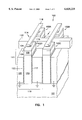
- FIG. 1 is a perspective view of an embodiment of a portion of an array of memory cells indicated generally at 100 and constructed according to the teachings of the present invention. Each memory cell is constructed in a similar manner. Thus, only memory cell 102D is described herein in detail.
- Memory cell 102D includes pillar 104 of single crystal semiconductor material. Pillar 104 is divided into first source/drain region 106, body region 108, and second source/drain region 110 to form access transistor 111. Pillar 104 extends vertically outward from substrate 101, for example, p- silicon.
- First source/drain region 106 and second source/drain region 110 each comprise, for example, heavily doped n-type single crystalline silicon (N+ silicon) and body region 108 comprises lightly doped p-type single crystalline silicon (P- silicon).
- Word line 112 passes body region 108 of access transistor 111 in isolation trench 114.
- Word line 112 is separated from body region 108 of access transistor 104 by gate oxide 116 such that the portion of word line 112 adjacent to body region 108 operates as a gate for access transistor 111.
- Word line 112 may comprise, for example, N+ poly-silicon material that is deposited in isolation trench 114.
- Cell 102D is coupled in a column with cell 102A by bit line 118.
- Memory cell 102D also includes storage capacitor 119 for storing data in the cell.
- a first plate of capacitor 119 for memory cell 102D is integral with second source/drain region 110 of access transistor 111.
- memory cell 102D may be more easily realizable when compared to conventional vertical transistors since there is no need for a contact between second source/drain region 110 and capacitor 119.
- Surface 117 of second source/drain region 110 comprises a "micro-roughened” surface. This micro-roughened surface is formed by coating second source/drain region 110 with poly-silicon and treating the poly-silicon so as to form pores in surface 117. This increases the surface area of second source/drain region 110 and, thus, increases the capacitance of capacitor 119.
- the pores in surface 117 can be formed, for example, using the etching techniques described below.
- Second plate 120 of capacitor 119 is common to all of the capacitors of array 100.
- Second plate 120 comprises a mesh or grid of n+ poly-silicon formed in deep trenches that surrounds at least a portion of second source/drain region 110 of each pillar 104A through 104D.
- Second plate 120 is grounded by contact with substrate 101 underneath the trenches.
- Second plate 120 is separated from source/drain region 110 by gate insulator 122.
- FIGS. 2, 3, 4 and 5 are cross sectional views that illustrate an embodiment of a method for forming an array of memory cells according to the present invention.
- FIG. 2 is a cross sectional view that shows a portion of an array of memory cells, indicated generally at 200.
- Array 200 includes pillars of semiconductor material 202 and 204 that are formed either outwardly from a bulk silicon wafer or outwardly from a silicon-on-insulator (SOI) structure.
- Pillar 202 includes first source/drain region 206, body region 208 and second source/drain region 210. As shown, first source/drain region 206 and second source/drain region 210 comprise heavily doped n-type semiconductor material and body region 208 comprises p-type semiconductor material. Pillar 204 is similarly constructed. Pillars 202 and 204 form the basis for vertical transistors used in array 200. It is noted that the conductivity types of the various regions of the pillars can be swapped so as to allow the formation of p-channel transistors.
- the silicon pillar structure of a vertical transistor of array 200 may be formed using, for example, the techniques shown and described with respect to FIGS. 5A-5J of co-pending application Ser. No. 08/944,890, entitled “Circuit and Method for an Open Bit Line Memory Cell with A Vertical Transistor and Trench Plate Trench Capacitor,” filed on Oct. 6, 1997 or with respect to FIGS. 5A-5M of application Ser. No. 08/939,742, entitled “Circuit and Method for a Folded Bit Line Memory Cell with Vertical Transistors and a Trench Capacitor,” filed on Oct. 6, 1997, which applications are incorporated herein by reference.
- the silicon pillars can be constructed to provide for a body contact for the transistors using techniques described with respect to FIGS. 5A-5P and 6A to 6O of co-pending, commonly assigned application Ser. No. 08/944,312, entitled “Circuit and Method for a Folded Bit Line Memory Using Trench Plate Capacitor Cells With Body Bias Contacts,” filed on Oct. 6, 1997 or with respect to FIGS. 5A-5O of Application Ser. No. 08/939,732, entitled “Circuit and Method for an Open Bit Line Memory Cell With A Vertical Transistor and Trench Plate Trench Capacitor,” filed on Oct. 6, 1997, which applications are also incorporated herein by reference. Further, other conventional techniques for forming vertical transistors can also be used.
- nitride layer 212 Si 3 N 4
- nitride pad 213 is also deposited in trench 214 to protect the bottom of trench 214 during subsequent processing steps.
- nitride pad 213 may be used when an SOI structure is used and the bottom of trench 214 is an insulator such as an oxide.
- Trench 214 is filled with an oxide such that the entire structure of array 200 is covered.
- the oxide material outside of trench 214 is removed by, for example, chemical/mechanical polishing down to nitride layer 212.
- the oxide is further recessed into trench 214 to form oxide layer 216 as shown.
- Nitride masking layer 218 (Si 3 N 4 ) is next deposited to protect body region 208 and second source drain region 210 during the formation of a micro-roughened surface. It is noted that masking layer 218 can be formed of any other material that can withstand a 6% aqueous solution of hydrofluoric acid (HF) or other etchant used to form a micro-roughened surface on first source/drain region 206.
- HF hydrofluoric acid
- nitride mask layer 218 is directionally etched to leave nitride mask layer 218 on selected surfaces of pillars 202 and 204.
- Oxide layer 216 is removed by, for example, an etching process.
- Amorphous silicon is deposited in trench 214 to form layer 220 with a thickness on the order of 10 to 40 nanometers (nm).
- the structure is heated to a sufficient temperature such that impurities diffuse out from first source/drain region 206 into layer 220.
- layer 220 becomes polysilicon that is doped to be the same conductivity type as first source/drain region 206.
- An etch that preferentially attacks intrinsic, undoped polysilicon is used to remove layer 220 from surfaces other than the surface of first source/drain region 206.
- Surface 221 of layer 220 is next roughened to provide increased surface area for the trench capacitors of array 200.
- Surface 221 can be roughened in at least two different ways. First, layer 220 can be etched in a solution containing phosphoric acid (H 3 PO 4 ). This forms micro-roughened surface 222 on polysilicon layer 220 in trench 214 as shown in FIG. 4.
- H 3 PO 4 phosphoric acid
- FIG. 5 is a schematic diagram that illustrates an embodiment of a layout of equipment used to carry out the anodic etch.
- Bottom surface 246 of semiconductor wafer 201 is coupled to voltage source 234 by positive electrode 230.
- negative electrode 232 is coupled to voltage source 234 and is placed in a bath of 6% aqueous solution of hydrofluoric acid (HF) on surface 245 of semiconductor wafer 201.
- HF hydrofluoric acid
- illumination equipment 236 is also included because the surface to be roughened is n-type semiconductor material. When p-type semiconductor material is used, the illumination equipment is not required. Illumination equipment 236 assures that there is a sufficient concentration of holes in layer 220 as required by the anodic etching process. Illumination equipment 236 includes lamp 238, IR filter 240, and lens 242. Illumination equipment 236 focuses light on surface 246 of semiconductor wafer 201.
- layer 220 provides a high density of nucleation sites that are used by the anodic etch to roughen the surface of layer 220.
- Voltage source 234 is turned on and provides a voltage across positive and negative electrodes 230 and 232.
- Etching current flows from positive electrode 230 to surface 245. This current forms pores in surface 221 of layer 220.
- illumination equipment illuminates surface 246 of semiconductor wafer 201 so as to assure a sufficient concentration of holes for the anodic etching process.
- the anodic etching process produces a porous or roughened surface 222 on layer 220 as shown in FIG. 4 such that the effective surface area of first source/drain region 206 is increased.
- the size and shape of the pores in layer 220 depends on, for example, the anodization parameters such as HF concentration, current density, and light illumination.
- the spatial structure of the pores reflects the available paths for the etching current to flow from surface 245 to positive electrode 230.
- the approximate diameter of the pores can be controlled with typically the smallest pore diameter on the order of 2 nanometers.
- Array 200 is completed using, for example, the techniques described in the applications incorporated by reference above.
- FIG. 6 is a cross sectional view of another embodiment of a memory cell according to the teachings of the present invention.
- Memory cell 600 includes a conventional lateral transistor 602 with first source/drain region 604, body region 606 and second source/drain region 608.
- Transistor 602 also includes gate 610 that may be formed as part of a word line in a memory array as is known in the art.
- Bit line 612 is coupled to first source/drain region 604.
- Memory cell 600 also includes trench capacitor 614.
- Substrate 616 forms a first plate of trench capacitor 614.
- Surface 618 of substrate 616 in trench 620 is formed with a micro-roughened surface using, for example, one of the techniques described above by depositing and etching a polysilicon layer in trench 620.
- Trench capacitor 614 also includes dielectric layer 622 that separates surface 618 from second plate 624.
- Second plate 624 comprises, for example, poly-silicon.
- Substrate 616 comprises single crystal silicon. A layer of polysilicon material is deposited on a surface of the single crystal silicon of substrate 616 in forming micro-roughened surface 618. Second plate 624 of trench capacitor 614 is coupled to second source/drain region 608 by polysilicon strap 630.
- transistor 602 comprises an n-channel transistor with heavily doped n-type source/drain regions and a body region formed in lightly doped p-type silicon well.
- substrate 616 comprises a heavily doped p-type semiconductor substrate. Since substrate 616 comprises p-type material, the anodic etch, without illumination, can be used to form micro-roughened surface 618.
- Memory cell 600 is included in an array of similar memory cells to store and retrieve data using conventional techniques.
- FIG. 7 is a block diagram of an illustrative embodiment of the present invention.
- This embodiment includes memory device 700 that is coupled to electronic system 702 by control lines 704, address lines 706 and input/output (I/O) lines 708.
- Electronic system 702 comprises, for example, a microprocessor, a processor based computer, microcontroller, memory controller, a chip set or other appropriate system for reading and writing data in a memory device.
- Memory device 700 includes array of memory cells 710 that is coupled to word line decoder 714 and sense amplifier 711.
- Array of memory cells 710 is constructed with memory cells that include trench capacitors with a micro-roughened surface that is formed using, for example, one of the techniques described above.
- Word line decoder 714 includes word line drivers that are coupled to word lines of array 710.
- Sense amplifier 711 is coupled to bit line decoder 712.
- Bit line decoder 712 and word line decoder 714 are coupled to address lines 706.
- Bit line decoder 712 is coupled to I/O circuit 716.
- I/O circuit 716 is coupled to I/O lines 708.
- Control circuit 718 is coupled to control lines 704, sense amplifier 711, word line decoder 714, bit line decoder 712, and I/O circuit 716.
- electronic system 702 provides signals on address lines 706 and control lines 704 when data is to be read from or written to a cell of array 710.
- Word line decoder 714 determines the word line of a selected cell of array 710 using the address provided on address lines 706.
- bit line decoder 712 determines the bit line of the selected cell of array 710.
- sense amplifier 711 detects the value stored in the selected cell based on bit lines of array 710.
- Sense amplifier 711 provides this voltage to I/O circuit 716 which, in turn, passes data to electronic system 702 over I/0 lines 708.
- I/O circuit 716 passes data from I/O lines 708 to sense amplifier 711 for storage in the selected cell of array 710.
- the techniques for forming roughened surfaces can be applied to p-type vertical transistors. In this case, when an anodic etch is used, no light source is needed to create the roughened texture on the surface of the p-type semiconductor material. Semiconductor materials other than silicon can be used. Further, the conductivity type of the semiconductor material can be altered without departing from the teachings of the present invention.
Abstract
A method for forming a trench capacitor. The method includes forming a trench in a semiconductor substrate. A conformal layer of semiconductor material is deposited in the trench. The surface of the conformal layer of semiconductor material is roughened. An insulator layer is formed outwardly from the roughened, conformal layer of semiconductor material. A polycrystalline semiconductor plate is formed outwardly from the insulator layer in the trench.
Description
The present invention relates generally to the field of integrated circuits and, in particular, to circuits with a trench capacitor having micro-roughened semiconductor surfaces and methods for forming the same.
Electronic systems, such as microprocessor based computers, typically operate on data that is stored in electronic form in a memory device. The memory device stores the data at specified voltage levels in an array of cells. Conventionally, the voltage levels represent that the data is either a logical "1" or a logical "0." In dynamic random access memory (DRAM) devices, for example, the cells store the data as a charge on a capacitor. When the data is read from the memory device, sense amplifiers detect the level of charge stored on a particular capacitor so as to produce a logical "1" or a logical "0" output based on the stored charge.
As the size of memory devices decreases, the capacitor in each cell covers a smaller surface area or footprint on the substrate, chip or wafer. If the structure of the capacitor is left unchanged, these smaller capacitors cannot store as much charge because the storage capacity of a typical capacitor is proportional to the size of its storage electrodes. Unfortunately, at some point, the capacitors become too small to store sufficient charge and sense amplifiers in the memory device are unable to differentiate between charge due to noise and the charge due to data stored in the cell. This can lead to errors in the output of a memory device making the memory device useless in the electronic system.
Conventionally, memory manufacturers have used one of two types of capacitors in DRAM devices. First, many manufacturers use "stacked" capacitors to store data for the memory cell. Stacked capacitors are typically formed from polysilicon and are positioned above the conventional working surface of the semiconductor chip or wafer on which the memory device is formed. A contact couples the capacitor to a transistor in the memory cell. Some manufacturers use "tench" capacitors instead of stacked capacitors. Trench capacitors are typically formed in a trench in the semiconductor wafer or chip. The trench is filled with polysilicon that acts as one plate of the capacitor. In this case, the semiconductor wafer or chip acts as the second plate of the capacitor.
Designers have experimented with various configurations of capacitors, both stacked and trench, to maintain the capacitance as the footprint available for the capacitor decreases. In the area of stacked capacitors, designers have used texturization, stacked V-shaped plates and other shaped plates to increase the surface area of the plates without increasing the footprint of the capacitor. For example, designers have developed techniques to produce hemispherical grains on the surface of one polysilicon plate of the stacked capacitor. This roughly doubles the storage capacity of the capacitor. Researchers have also described techniques for further increasing the surface area of the polysilicon plate, and thus the storage capacity of the capacitor, by using phosphoric acid to create pores in the polysilicon plate. See, Watanabe, A Novel Stacked Capacitor with Porous-Si Electrodesfor High Density DRAMs, Symposium on VLSI Technology, pp. 17-18, 1993. With this technique, it is claimed that a 3.4 times increase in capacitance can be achieved.
One problem with the use of stacked capacitors is their positioning above the surface of the substrate. This positioning can interfere with the proper functioning of the equipment used to fabricate other parts of a larger circuit.
Conventionally, as the footprint available for trench capacitors has decreased, the manufacturers have used deeper trenches to maintain sufficient storage capacity of the trench capacitor. IBM has developed another technique in an attempt to maintain sufficient storage capacity as the footprint of the trench capacitor decreases. This technique uses an anodic etch to create pores in the single crystalline silicon in the trench of the trench capacitor. See, U.S. Pat. No. 5,508,542 (the '542 Patent). One problem with this technique is the lack of control over the distribution of the pores in the surface of the single crystalline silicon. Thus, the '542 Patent does not provide a technique that can be used reliably for large scale production of memory devices.
For the reasons stated above, and for other reasons stated below which will become apparent to those skilled in the art upon reading and understanding the present specification, there is a need in the art for a realizable trench capacitor with increased surface area compared to prior art capacitors for use in high-density circuits such as dynamic random access memories.
The above mentioned problems with integrated circuits and other problems are addressed by the present invention and which will be understood by reading and studying the following specification. A trench capacitor with increased surface area is described which is formed by depositing a layer of polysilicon in a trench in a semiconductor substrate and etching the polysilicon to produce a porous surface for the trench capacitor.
In particular, an illustrative embodiment of the present invention includes a method for forming a trench capacitor. The method includes forming a trench in a semiconductor substrate. A conformal layer of semiconductor material is deposited in the trench. The surface of the conformal layer of semiconductor material is roughened. An insulator layer is formed outwardly from the roughened, conformal layer of semiconductor material. A polycrystalline semiconductor plate is formed outwardly from the insulator layer in the trench.
In another embodiment, a method for forming a memory cell with a trench capacitor is provided. The method includes forming a transistor including first and second source/drain regions, a body region and a gate in a layer of semiconductor material on a substrate. Further, a trench is formed in the layer of semiconductor material and a conformal layer of semiconductor material is formed in the trench. The surface of the conformal layer of semiconductor material is roughened and an insulator layer is formed outwardly from the roughened, conformal layer of semiconductor material. A polycrystalline semiconductor plate is formed outwardly from the insulator layer in the trench such that the polycrystalline semiconductor plate forms one of the plates of the trench capacitor. The trench capacitor is coupled to one of the first source/drain regions of the transistor.
In another embodiment, a memory cell is provided. The memory cell includes a lateral transistor formed in a layer of semiconductor material outwardly from a substrate. The transistor includes a first source/drain region, a body region and a second source/drain region. A trench capacitor is formed in a trench and coupled to the first source/drain region. The trench capacitor includes a polycrystalline semiconductor plate formed in the trench that is coupled to the first source/drain region. The trench capacitor also includes a second plate formed by the substrate with a surface of the substrate in the trench roughened by etching a polycrystalline semiconductor material on the surface of the substrate. The trench capacitor also includes an insulator layer that separates the polycrystalline semiconductor plate from the roughened surface of the substrate.
In another embodiment, a memory cell is provided. The memory cell includes a vertical transistor that is formed outwardly from a substrate. The transistor includes a first source/drain region, a body region and a second source/drain region that are vertically aligned. A surface of the first source/drain region is roughened by etching a polycrystalline semiconductor material on a surface of the first source/drain region. A trench capacitor is also included. The trench capacitor includes a plate that is formed in a trench that surrounds the roughened surface of the first source/drain region of the transistor.
In another embodiment, a memory device is provided. The memory device includes an array of memory cells. Each memory cell includes an access transistor that is coupled to a trench capacitor. A first plate of the trench capacitor includes a micro-roughened surface of porous polysilicon. A second plate of the trench capacitor is disposed adjacent to the first plate. A number of bit lines are each selectively coupled to a number of the memory cells at a first source/drain region of the access transistor. A number of word lines are disposed substantially orthogonal to the bit lines and are coupled to gates of a number of access transistors. A row decoder is coupled to the word lines and a column decoder is coupled to the bit lines so as to selectively access the cells of the array.
FIG. 1 is a perspective view of an embodiment of a portion of an array of memory cells according to the teachings of the present invention.
FIGS. 2, 3, 4 and 5 are cross sectional views that illustrate an embodiment of a method for forming an array of memory cells according to the teachings of the present invention.
FIG. 6 is a cross sectional view of another embodiment of a memory cell according to the teachings of the present invention.
FIG. 7 is a block diagram of an embodiment of an electronic system and memory device according to the teachings of the present invention.
In the following detailed description of the preferred embodiments, reference is made to the accompanying drawings which form a part hereof, and in which is shown by way of illustration specific illustrative embodiments in which the invention may be practiced. These embodiments are described in sufficient detail to enable those skilled in the art to practice the invention, and it is to be understood that other embodiments may be utilized and that logical, mechanical and electrical changes may be made without departing from the spirit and scope of the present invention. The following detailed description is, therefore, not to be taken in a limiting sense.
In the following description, the terms wafer and substrate are interchangeably used to refer generally to any structure on which integrated circuits are formed, and also to such structures during various stages of integrated circuit fabrication. Both terms include doped and undoped semiconductors, epitaxial layers of a semiconductor on a supporting semiconductor or insulating material, combinations of such layers, as well as other such structures that are known in the art.
The term "horizontal" as used in this application is defined as a plane parallel to the conventional plane or surface of a wafer or substrate, regardless of the orientation of the wafer or substrate. The term "vertical" refers to a direction perpendicular to the horizonal as defined above. Prepositions, such as "on", "side" (as in "sidewall"), "higher", "lower", "over" and "under" are defined with respect to the conventional plane or surface being on the top surface of the wafer or substrate, regardless of the orientation of the wafer or substrate.
FIG. 1 is a perspective view of an embodiment of a portion of an array of memory cells indicated generally at 100 and constructed according to the teachings of the present invention. Each memory cell is constructed in a similar manner. Thus, only memory cell 102D is described herein in detail. Memory cell 102D includes pillar 104 of single crystal semiconductor material. Pillar 104 is divided into first source/drain region 106, body region 108, and second source/drain region 110 to form access transistor 111. Pillar 104 extends vertically outward from substrate 101, for example, p- silicon. First source/drain region 106 and second source/drain region 110 each comprise, for example, heavily doped n-type single crystalline silicon (N+ silicon) and body region 108 comprises lightly doped p-type single crystalline silicon (P- silicon).
FIGS. 2, 3, 4 and 5 are cross sectional views that illustrate an embodiment of a method for forming an array of memory cells according to the present invention. FIG. 2 is a cross sectional view that shows a portion of an array of memory cells, indicated generally at 200. Array 200 includes pillars of semiconductor material 202 and 204 that are formed either outwardly from a bulk silicon wafer or outwardly from a silicon-on-insulator (SOI) structure. Pillar 202 includes first source/drain region 206, body region 208 and second source/drain region 210. As shown, first source/drain region 206 and second source/drain region 210 comprise heavily doped n-type semiconductor material and body region 208 comprises p-type semiconductor material. Pillar 204 is similarly constructed. Pillars 202 and 204 form the basis for vertical transistors used in array 200. It is noted that the conductivity types of the various regions of the pillars can be swapped so as to allow the formation of p-channel transistors.
The silicon pillar structure of a vertical transistor of array 200 may be formed using, for example, the techniques shown and described with respect to FIGS. 5A-5J of co-pending application Ser. No. 08/944,890, entitled "Circuit and Method for an Open Bit Line Memory Cell with A Vertical Transistor and Trench Plate Trench Capacitor," filed on Oct. 6, 1997 or with respect to FIGS. 5A-5M of application Ser. No. 08/939,742, entitled "Circuit and Method for a Folded Bit Line Memory Cell with Vertical Transistors and a Trench Capacitor," filed on Oct. 6, 1997, which applications are incorporated herein by reference. Alternatively, the silicon pillars can be constructed to provide for a body contact for the transistors using techniques described with respect to FIGS. 5A-5P and 6A to 6O of co-pending, commonly assigned application Ser. No. 08/944,312, entitled "Circuit and Method for a Folded Bit Line Memory Using Trench Plate Capacitor Cells With Body Bias Contacts," filed on Oct. 6, 1997 or with respect to FIGS. 5A-5O of Application Ser. No. 08/939,732, entitled "Circuit and Method for an Open Bit Line Memory Cell With A Vertical Transistor and Trench Plate Trench Capacitor," filed on Oct. 6, 1997, which applications are also incorporated herein by reference. Further, other conventional techniques for forming vertical transistors can also be used.
Once the basic silicon pillar structure is in place, surface 209 of first source/drain region 206 is roughened. Initially, nitride layer 212 (Si3 N4) is deposited on silicon pillars 202 and 204. Optionally, nitride pad 213 is also deposited in trench 214 to protect the bottom of trench 214 during subsequent processing steps. For example, nitride pad 213 may be used when an SOI structure is used and the bottom of trench 214 is an insulator such as an oxide.
As shown in FIG. 3, nitride mask layer 218 is directionally etched to leave nitride mask layer 218 on selected surfaces of pillars 202 and 204. Oxide layer 216 is removed by, for example, an etching process. Amorphous silicon is deposited in trench 214 to form layer 220 with a thickness on the order of 10 to 40 nanometers (nm). The structure is heated to a sufficient temperature such that impurities diffuse out from first source/drain region 206 into layer 220. Thus, layer 220 becomes polysilicon that is doped to be the same conductivity type as first source/drain region 206. An etch that preferentially attacks intrinsic, undoped polysilicon is used to remove layer 220 from surfaces other than the surface of first source/drain region 206.
Surface 221 of layer 220 is next roughened to provide increased surface area for the trench capacitors of array 200. Surface 221 can be roughened in at least two different ways. First, layer 220 can be etched in a solution containing phosphoric acid (H3 PO4). This forms micro-roughened surface 222 on polysilicon layer 220 in trench 214 as shown in FIG. 4.
Alternatively, an anodic etch can be used to form the micro-roughened surface on layer 220. FIG. 5 is a schematic diagram that illustrates an embodiment of a layout of equipment used to carry out the anodic etch. Bottom surface 246 of semiconductor wafer 201 is coupled to voltage source 234 by positive electrode 230. Further, negative electrode 232 is coupled to voltage source 234 and is placed in a bath of 6% aqueous solution of hydrofluoric acid (HF) on surface 245 of semiconductor wafer 201. It is noted that surface 245 includes layer 220 that is to be roughened by the anodic etch.
In this example, illumination equipment 236 is also included because the surface to be roughened is n-type semiconductor material. When p-type semiconductor material is used, the illumination equipment is not required. Illumination equipment 236 assures that there is a sufficient concentration of holes in layer 220 as required by the anodic etching process. Illumination equipment 236 includes lamp 238, IR filter 240, and lens 242. Illumination equipment 236 focuses light on surface 246 of semiconductor wafer 201.
In operation, layer 220 provides a high density of nucleation sites that are used by the anodic etch to roughen the surface of layer 220. Voltage source 234 is turned on and provides a voltage across positive and negative electrodes 230 and 232. Etching current flows from positive electrode 230 to surface 245. This current forms pores in surface 221 of layer 220. Further, illumination equipment illuminates surface 246 of semiconductor wafer 201 so as to assure a sufficient concentration of holes for the anodic etching process. The anodic etching process produces a porous or roughened surface 222 on layer 220 as shown in FIG. 4 such that the effective surface area of first source/drain region 206 is increased.
The size and shape of the pores in layer 220 depends on, for example, the anodization parameters such as HF concentration, current density, and light illumination. The spatial structure of the pores reflects the available paths for the etching current to flow from surface 245 to positive electrode 230. By adjusting the anodic etching parameters, the approximate diameter of the pores can be controlled with typically the smallest pore diameter on the order of 2 nanometers.
FIG. 6 is a cross sectional view of another embodiment of a memory cell according to the teachings of the present invention. Memory cell 600 includes a conventional lateral transistor 602 with first source/drain region 604, body region 606 and second source/drain region 608. Transistor 602 also includes gate 610 that may be formed as part of a word line in a memory array as is known in the art. Bit line 612 is coupled to first source/drain region 604.
In the example of FIG. 6, transistor 602 comprises an n-channel transistor with heavily doped n-type source/drain regions and a body region formed in lightly doped p-type silicon well. Further, substrate 616 comprises a heavily doped p-type semiconductor substrate. Since substrate 616 comprises p-type material, the anodic etch, without illumination, can be used to form micro-roughened surface 618.
FIG. 7 is a block diagram of an illustrative embodiment of the present invention. This embodiment includes memory device 700 that is coupled to electronic system 702 by control lines 704, address lines 706 and input/output (I/O) lines 708. Electronic system 702 comprises, for example, a microprocessor, a processor based computer, microcontroller, memory controller, a chip set or other appropriate system for reading and writing data in a memory device. Memory device 700 includes array of memory cells 710 that is coupled to word line decoder 714 and sense amplifier 711. Array of memory cells 710 is constructed with memory cells that include trench capacitors with a micro-roughened surface that is formed using, for example, one of the techniques described above.
In operation, electronic system 702 provides signals on address lines 706 and control lines 704 when data is to be read from or written to a cell of array 710. Word line decoder 714 determines the word line of a selected cell of array 710 using the address provided on address lines 706. Further, bit line decoder 712 determines the bit line of the selected cell of array 710. In a read operation, sense amplifier 711 detects the value stored in the selected cell based on bit lines of array 710. Sense amplifier 711 provides this voltage to I/O circuit 716 which, in turn, passes data to electronic system 702 over I/0 lines 708. In a write operation, I/O circuit 716 passes data from I/O lines 708 to sense amplifier 711 for storage in the selected cell of array 710.
Although specific embodiments have been illustrated and described herein, it will be appreciated by those of ordinary skill in the art that any arrangement which is calculated to achieve the same purpose may be substituted for the specific embodiment shown. This application is intended to cover any adaptations or variations of the present invention. For example, the techniques for forming roughened surfaces can be applied to p-type vertical transistors. In this case, when an anodic etch is used, no light source is needed to create the roughened texture on the surface of the p-type semiconductor material. Semiconductor materials other than silicon can be used. Further, the conductivity type of the semiconductor material can be altered without departing from the teachings of the present invention.
Claims (30)
1. A method for forming a trench capacitor, the method comprising:
forming a trench in a semiconductor substrate;
depositing a conformal layer of semiconductor material in the trench;
heating the conformal layer of semiconductor material to form a layer of the same conductivity type as the adjacent semiconductor substrate;
roughening the surface of the conformal layer of semiconductor material;
forming an insulator layer outwardly from the roughened, conformal layer of semiconductor material; and
forming a polycrystalline semiconductor plate outwardly from the insulator layer in the trench.
2. The method of claim 1, wherein roughening the surface of the conformal layer of semiconductor material comprises etching a surface of the semiconductor material with a phosphoric acid etch.
3. The method of claim 1, wherein roughening the surface of the conformal layer of semiconductor material comprises etching a surface of the semiconductor material with an anodic etch.
4. The method of claim 1, wherein forming an insulator layer comprises growing an oxide layer outwardly from the roughened, conformal layer of semiconductor material.
5. A method for forming a memory cell with a trench capacitor, comprising:
forming a transistor including first and second source/drain regions, a body region and a gate in a layer of semiconductor material on a substrate;
forming a trench in the layer of semiconductor material;
depositing a conformal layer of semiconductor material in the trench;
roughening the surface of the conformal layer of semiconductor material performing an anodic etch of a surface of the semiconductor material;
forming an insulator layer outwardly from the roughened, conformal layer of semiconductor material;
forming a polycrystalline semiconductor plate outwardly from the insulator layer in the trench such that the polycrystalline semiconductor plate forms one of the plates of the trench capacitor; and
coupling the trench capacitor to one of the source/drain regions of the transistor.
6. The method of claim 5, wherein forming a transistor comprises forming a transistor with first and second source drain regions that are vertically aligned with the body region.
7. The method of claim 6, wherein coupling the trench capacitor to the first source/drain region comprises forming the trench for the trench capacitor adjacent to the first source/drain region.
8. The method of claim 5, wherein forming a transistor comprises forming a lateral transistor.
9. The method of claim 8, wherein coupling the trench capacitor to the first source/drain region comprises forming a strap from the polycrystalline semiconductor plate to the first source/drain region.
10. The method of claim 5, wherein depositing a conformal layer of semiconductor material comprises depositing a layer of amorphous silicon and heating the amorphous silicon to form a poly-silicon layer of the same conductivity type as the adjacent semiconductor substrate.
11. The method of claim 5, wherein forming an insulator layer comprises growing an oxide layer outwardly from the roughened, conformal layer of semiconductor material.
12. A method for forming a trench capacitor, the method comprising:
forming a trench in a semiconductor substrate;
depositing a conformal layer of semiconductor material in the trench;
roughening the surface of the conformal layer of semiconductor material by etching a surface of the semiconductor material with an anodic etch including illuminating the conformal layer of semiconductor material during the anodic etch;
forming an insulator layer outwardly from the roughened, conformal layer of semiconductor material; and
forming a polycrystalline semiconductor plate outwardly from the insulator layer in the trench.
13. The method of claim 12, wherein depositing a conformal layer of semiconductor material comprises depositing a layer of amorphous silicon and heating the amorphous silicon to form a polysilicon layer of the same conductivity type as the adjacent semiconductor substrate.
14. The method of claim 12, wherein forming an insulator layer comprises growing an oxide layer outwardly from the roughened, conformal layer of semiconductor material.
15. A method for forming a memory cell with a trench capacitor, comprising:
forming a transistor including first and second source/drain regions, a body region and a gate in a layer of semiconductor material on a substrate;
forming a trench in the layer of semiconductor material;
depositing a conformal layer of semiconductor material in the trench;
roughening the surface of the conformal layer of semiconductor material by performing an anodic etch of a surface of the semiconductor material while illuminating the semiconductor material;
forming an insulator layer outwardly from the roughened, conformal layer of semiconductor material;
forming a polycrystalline semiconductor plate outwardly from the insulator layer in the trench such that the polycrystalline semiconductor plate forms one of the plates of the trench capacitor; and
coupling the trench capacitor to one of the source/drain regions of the transistor.
16. The method of claim 15, wherein forming a transistor comprises forming a transistor with first and second source drain regions that are vertically aligned with the body region.
17. The method of claim 16, wherein coupling the trench capacitor to the first source/drain region comprises forming the trench for the trench capacitor adjacent to the first source/drain region.
18. The method of claim 15, wherein forming a transistor comprises formiing a lateral transistor.
19. The method of claim 18, wherein coupling the trench capacitor to the first source/drain region comprises forming a strap from the polycrystalline semiconductor plate to the first source/drain region.
20. The method of claim 15, wherein depositing a conformal layer of semiconductor material comprises depositing a layer of amorphous silicon and heating the amorphous silicon to form a poly-silicon layer of the same conductivity type as the adjacent semiconductor substrate.
21. The method of claim 15, wherein forming an insulator layer comprises growing an oxide layer outwardly from the roughened, conformal layer of semiconductor material.
22. A method for forming a trench capacitor, the method comprising:
forming a trench in a semiconductor substrate;
depositing a conformal layer of semiconductor material in the trench;
roughening the surface of the conformal layer of semiconductor material by etching a surface of the semiconductor material with an anodic etch;
forming an insulator layer outwardly from the roughened, conformal layer of semiconductor material; and
forming a polycrystalline semiconductor plate outwardly from the insulator layer in the trench.
23. The method of claim 22, wherein forming an insulator layer comprises growing an oxide layer outwardly from the roughened, conformal layer of semiconductor material.
24. A method for forming a memory cell with a trench capacitor, comprising:
forming a transistor including first and second source/drain regions, a body region and a gate in a layer of semiconductor material on a substrate;
forming a trench in the layer of semiconductor material;
depositing a conformal layer of semiconductor material in the trench by depositing a layer of amorphous silicon and heating the amorphous silicon to form a poly-silicon layer of the same conductivity type as the adjacent semiconductor substrate;
roughening the surface of the conformal layer of semiconductor material;
forming an insulator layer outwardly from the roughened, conformal layer of semiconductor material;
forming a polycrystalline semiconductor plate outwardly from the insulator layer in the trench such that the polycrystalline semiconductor plate forms one of the plates of the trench capacitor; and
coupling the trench capacitor to one of the source/drain regions of the transistor.
25. The method of claim 24, wherein forming a transistor comprises forming a transistor with first and second source drain regions that are vertically aligned with the body region.
26. The method of claim 25, wherein coupling the trench capacitor to the first source/drain region comprises forming the trench for the trench capacitor adjacent to the first source/drain region.
27. The method of claim 24, wherein forming a transistor comprises forming a lateral transistor.
28. The method of claim 27, wherein coupling the trench capacitor to the first source/drain region comprises forming a strap from the polycrystalline semiconductor plate to the first source/drain region.
29. The method of claim 24, wherein roughening the surface of the conformal layer of semiconductor material comprises etching a surface of the semiconductor material with phosphoric acid.
30. The method of claim 24, wherein forming an insulator layer comprises growing an oxide layer outwardly from the roughened, conformal layer of semiconductor material.
Priority Applications (3)
| Application Number | Priority Date | Filing Date | Title |
|---|---|---|---|
| US09/010,729 US6025225A (en) | 1998-01-22 | 1998-01-22 | Circuits with a trench capacitor having micro-roughened semiconductor surfaces and methods for forming the same |
| US09/467,992 US7084451B2 (en) | 1998-01-22 | 1999-12-20 | Circuits with a trench capacitor having micro-roughened semiconductor surfaces |
| US11/484,541 US7408216B2 (en) | 1998-01-22 | 2006-07-11 | Device, system, and method for a trench capacitor having micro-roughened semiconductor surfaces |
Applications Claiming Priority (1)
| Application Number | Priority Date | Filing Date | Title |
|---|---|---|---|
| US09/010,729 US6025225A (en) | 1998-01-22 | 1998-01-22 | Circuits with a trench capacitor having micro-roughened semiconductor surfaces and methods for forming the same |
Related Child Applications (1)
| Application Number | Title | Priority Date | Filing Date |
|---|---|---|---|
| US09/467,992 Division US7084451B2 (en) | 1998-01-22 | 1999-12-20 | Circuits with a trench capacitor having micro-roughened semiconductor surfaces |
Publications (1)
| Publication Number | Publication Date |
|---|---|
| US6025225A true US6025225A (en) | 2000-02-15 |
Family
ID=21747116
Family Applications (3)
| Application Number | Title | Priority Date | Filing Date |
|---|---|---|---|
| US09/010,729 Expired - Fee Related US6025225A (en) | 1998-01-22 | 1998-01-22 | Circuits with a trench capacitor having micro-roughened semiconductor surfaces and methods for forming the same |
| US09/467,992 Expired - Fee Related US7084451B2 (en) | 1998-01-22 | 1999-12-20 | Circuits with a trench capacitor having micro-roughened semiconductor surfaces |
| US11/484,541 Expired - Fee Related US7408216B2 (en) | 1998-01-22 | 2006-07-11 | Device, system, and method for a trench capacitor having micro-roughened semiconductor surfaces |
Family Applications After (2)
| Application Number | Title | Priority Date | Filing Date |
|---|---|---|---|
| US09/467,992 Expired - Fee Related US7084451B2 (en) | 1998-01-22 | 1999-12-20 | Circuits with a trench capacitor having micro-roughened semiconductor surfaces |
| US11/484,541 Expired - Fee Related US7408216B2 (en) | 1998-01-22 | 2006-07-11 | Device, system, and method for a trench capacitor having micro-roughened semiconductor surfaces |
Country Status (1)
| Country | Link |
|---|---|
| US (3) | US6025225A (en) |
Cited By (65)
| Publication number | Priority date | Publication date | Assignee | Title |
|---|---|---|---|---|
| US6121084A (en) * | 2000-01-27 | 2000-09-19 | Micron Technology, Inc. | Semiconductor processing methods of forming hemispherical grain polysilicon layers, methods of forming capacitors, and capacitors |
| US6153468A (en) * | 1998-02-27 | 2000-11-28 | Micron Technololgy, Inc. | Method of forming a logic array for a decoder |
| US6191003B1 (en) * | 1999-10-06 | 2001-02-20 | Mosel Vitelic Inc. | Method for planarizing a polycrystalline silicon layer deposited on a trench |
| US6195281B1 (en) | 1999-06-28 | 2001-02-27 | Hyundai Electronics Industries Co., Ltd. | Apparatus for generating reference voltage in ferroelectric memory device |
| US6232171B1 (en) * | 1999-01-11 | 2001-05-15 | Promos Technology, Inc. | Technique of bottle-shaped deep trench formation |
| US6235569B1 (en) | 1998-03-30 | 2001-05-22 | Micron Technology, Inc. | Circuit and method for low voltage, voltage sense amplifier |
| US6288931B1 (en) | 1999-06-28 | 2001-09-11 | Hyundai Electronics Industries Co., Ltd. | Ferroelectric memory device having cell groups containing capacitors commonly coupled to transistor |
| US6303954B1 (en) | 1998-06-11 | 2001-10-16 | Nec Corporation | Semiconductor device with a high-voltage component in semiconductor on insulator |
| US6307235B1 (en) * | 1998-03-30 | 2001-10-23 | Micron Technology, Inc. | Another technique for gated lateral bipolar transistors |
| US6346455B1 (en) | 2000-08-31 | 2002-02-12 | Micron Technology, Inc. | Method to form a corrugated structure for enhanced capacitance |
| US6381168B2 (en) | 1998-04-14 | 2002-04-30 | Micron Technology, Inc. | Circuits and methods for a memory cell with a trench plate trench capacitor and a vertical bipolar read device |
| US6380575B1 (en) * | 1999-08-31 | 2002-04-30 | International Business Machines Corporation | DRAM trench cell |
| US6449186B2 (en) * | 1998-02-24 | 2002-09-10 | Micron Technology, Inc. | Circuits and methods for a static random access memory using vertical transistors |
| US6448615B1 (en) | 1998-02-26 | 2002-09-10 | Micron Technology, Inc. | Methods, structures, and circuits for transistors with gate-to-body capacitive coupling |
| US6465298B2 (en) | 1997-07-08 | 2002-10-15 | Micron Technology, Inc. | Method of fabricating a semiconductor-on-insulator memory cell with buried word and body lines |
| US6486703B2 (en) | 1998-08-04 | 2002-11-26 | Micron Technology, Inc. | Programmable logic array with vertical transistors |
| US6486027B1 (en) | 1998-02-27 | 2002-11-26 | Micron Technology, Inc. | Field programmable logic arrays with vertical transistors |
| US20030045078A1 (en) * | 2001-08-30 | 2003-03-06 | Micron Technology, Inc. | Highly reliable amorphous high-K gate oxide ZrO2 |
| US6537871B2 (en) | 1997-10-06 | 2003-03-25 | Micron Technology, Inc. | Circuit and method for an open bit line memory cell with a vertical transistor and trench plate trench capacitor |
| US6555430B1 (en) * | 2000-11-28 | 2003-04-29 | International Business Machines Corporation | Process flow for capacitance enhancement in a DRAM trench |
| US20030142564A1 (en) * | 1997-10-06 | 2003-07-31 | Micron Technology, Inc. | Circuit and method for an open bit line memory cell with a vertical transistor and trench plate trench capacitor |
| US6613642B2 (en) | 2001-12-13 | 2003-09-02 | International Business Machines Corporation | Method for surface roughness enhancement in semiconductor capacitor manufacturing |
| US20030201479A1 (en) * | 2000-11-10 | 2003-10-30 | Albert Birner | Method for fabricating trench capacitors and semiconductor device with trench capacitors |
| US20030207593A1 (en) * | 2002-05-02 | 2003-11-06 | Micron Technology, Inc. | Atomic layer deposition and conversion |
| US20040023464A1 (en) * | 2002-06-19 | 2004-02-05 | Dietmar Temmler | Method for fabricating a deep trench capacitor for dynamic memory cells |
| US20040036131A1 (en) * | 2002-08-23 | 2004-02-26 | Micron Technology, Inc. | Electrostatic discharge protection devices having transistors with textured surfaces |
| US6706591B1 (en) | 2002-01-22 | 2004-03-16 | Taiwan Semiconductor Manufacturing Company | Method of forming a stacked capacitor structure with increased surface area for a DRAM device |
| US6709947B1 (en) | 2002-12-06 | 2004-03-23 | International Business Machines Corporation | Method of area enhancement in capacitor plates |
| US20040164365A1 (en) * | 2002-08-15 | 2004-08-26 | Micron Technology, Inc. | Lanthanide doped TiOx dielectric films |
| US20040219758A1 (en) * | 2001-10-19 | 2004-11-04 | Albert Birner | Method of forming a silicon dioxide layer |
| US6821864B2 (en) * | 2002-03-07 | 2004-11-23 | International Business Machines Corporation | Method to achieve increased trench depth, independent of CD as defined by lithography |
| US20040235243A1 (en) * | 1997-10-06 | 2004-11-25 | Micron Technology, Inc. | Circuit and method for a folded bit line memory cell with vertical transistor and trench capacitor |
| US20050026349A1 (en) * | 2001-08-30 | 2005-02-03 | Micron Technology, Inc. | Flash memory with low tunnel barrier interpoly insulators |
| US20050118775A1 (en) * | 2001-01-09 | 2005-06-02 | Matthias Goldbach | Method for fabricating trench capacitors for integrated semiconductor memories |
| US20060040148A1 (en) * | 2004-08-19 | 2006-02-23 | Gm Global Technology Operations, Inc. | Method of treating composite plates |
| US20060046505A1 (en) * | 2004-08-26 | 2006-03-02 | Micron Technology, Inc. | Ruthenium gate for a lanthanide oxide dielectric layer |
| US20060046522A1 (en) * | 2004-08-31 | 2006-03-02 | Micron Technology, Inc. | Atomic layer deposited lanthanum aluminum oxide dielectric layer |
| WO2006056959A1 (en) * | 2004-11-26 | 2006-06-01 | Koninklijke Philips Electronics N.V. | Method of modifying surface area and electronic device |
| US20060125030A1 (en) * | 2004-12-13 | 2006-06-15 | Micron Technology, Inc. | Hybrid ALD-CVD of PrxOy/ZrO2 films as gate dielectrics |
| US20060177975A1 (en) * | 2005-02-10 | 2006-08-10 | Micron Technology, Inc. | Atomic layer deposition of CeO2/Al2O3 films as gate dielectrics |
| US20060246652A1 (en) * | 2005-05-02 | 2006-11-02 | Semiconductor Components Industries, Llc. | Method of forming a semiconductor device and structure therefor |
| US20060244082A1 (en) * | 2005-04-28 | 2006-11-02 | Micron Technology, Inc. | Atomic layer desposition of a ruthenium layer to a lanthanide oxide dielectric layer |
| US20060249777A1 (en) * | 1998-01-22 | 2006-11-09 | Micron Technology, Inc. | Device, system, and method for a trench capacitor having micro-roughened semiconductor surfaces |
| US20070049054A1 (en) * | 2005-08-31 | 2007-03-01 | Micron Technology, Inc. | Cobalt titanium oxide dielectric films |
| US20070048926A1 (en) * | 2005-08-31 | 2007-03-01 | Micron Technology, Inc. | Lanthanum aluminum oxynitride dielectric films |
| US20070059881A1 (en) * | 2003-03-31 | 2007-03-15 | Micron Technology, Inc. | Atomic layer deposited zirconium aluminum oxide |
| US20070101929A1 (en) * | 2002-05-02 | 2007-05-10 | Micron Technology, Inc. | Methods for atomic-layer deposition |
| US20070178643A1 (en) * | 2002-07-08 | 2007-08-02 | Micron Technology, Inc. | Memory utilizing oxide-conductor nanolaminates |
| US20070181931A1 (en) * | 2005-01-05 | 2007-08-09 | Micron Technology, Inc. | Hafnium tantalum oxide dielectrics |
| US20070187831A1 (en) * | 2006-02-16 | 2007-08-16 | Micron Technology, Inc. | Conductive layers for hafnium silicon oxynitride films |
| US20090206316A1 (en) * | 2008-02-19 | 2009-08-20 | Qimonda Ag | Integrated circuit including u-shaped access device |
| US7728626B2 (en) | 2002-07-08 | 2010-06-01 | Micron Technology, Inc. | Memory utilizing oxide nanolaminates |
| US20100258904A1 (en) * | 2009-04-14 | 2010-10-14 | International Business Machines Corporation | Bottle-shaped trench capacitor with enhanced capacitance |
| US20100276748A1 (en) * | 2007-06-28 | 2010-11-04 | Ahn Kie Y | Method of forming lutetium and lanthanum dielectric structures |
| US20110045351A1 (en) * | 2009-08-23 | 2011-02-24 | Ramot At Tel-Aviv University Ltd. | High-Power Nanoscale Cathodes for Thin-Film Microbatteries |
| WO2011154862A1 (en) * | 2010-06-06 | 2011-12-15 | Ramot At Tel-Aviv University Ltd | Three-dimensional microbattery having a porous silicon anode |
| US20120127625A1 (en) * | 2010-11-18 | 2012-05-24 | Industrial Technology Research Institute | Trench capacitor structures and method of manufacturing the same |
| US8227311B2 (en) | 2010-10-07 | 2012-07-24 | International Business Machines Corporation | Method of forming enhanced capacitance trench capacitor |
| US8501563B2 (en) | 2005-07-20 | 2013-08-06 | Micron Technology, Inc. | Devices with nanocrystals and methods of formation |
| CN104246486A (en) * | 2012-05-15 | 2014-12-24 | 原子能和替代能源委员会 | Method for producing a capacitive sensor |
| US20170186837A1 (en) * | 2015-12-29 | 2017-06-29 | Taiwan Semiconductor Manufacturing Co., Ltd. | Deep trench capacitor with scallop profile |
| US20200020895A1 (en) * | 2018-07-11 | 2020-01-16 | International Business Machines Corporation | Silicon substrate containing integrated porous silicon electrodes for energy storage devices |
| US10826126B2 (en) | 2015-09-30 | 2020-11-03 | Ramot At Tel-Aviv University Ltd. | 3D micro-battery on 3D-printed substrate |
| US20210305360A1 (en) * | 2020-03-27 | 2021-09-30 | Lapis Semiconductor Co., Ltd. | Semiconductor device and manufacturing method for semiconductor device |
| US20220052316A1 (en) * | 2020-08-17 | 2022-02-17 | International Business Machines Corporation | Low reistance composite silicon-based electrode |
Families Citing this family (37)
| Publication number | Priority date | Publication date | Assignee | Title |
|---|---|---|---|---|
| US20050090053A1 (en) * | 2002-01-21 | 2005-04-28 | Infineon Technologies Ag | Memory chip with low-temperature layers in the trench capacitor |
| US7067385B2 (en) * | 2003-09-04 | 2006-06-27 | Micron Technology, Inc. | Support for vertically oriented capacitors during the formation of a semiconductor device |
| US7125781B2 (en) * | 2003-09-04 | 2006-10-24 | Micron Technology, Inc. | Methods of forming capacitor devices |
| US7387939B2 (en) | 2004-07-19 | 2008-06-17 | Micron Technology, Inc. | Methods of forming semiconductor structures and capacitor devices |
| US7202127B2 (en) | 2004-08-27 | 2007-04-10 | Micron Technology, Inc. | Methods of forming a plurality of capacitors |
| US7439152B2 (en) * | 2004-08-27 | 2008-10-21 | Micron Technology, Inc. | Methods of forming a plurality of capacitors |
| US20060046055A1 (en) * | 2004-08-30 | 2006-03-02 | Nan Ya Plastics Corporation | Superfine fiber containing grey dope dyed component and the fabric made of the same |
| US7320911B2 (en) * | 2004-12-06 | 2008-01-22 | Micron Technology, Inc. | Methods of forming pluralities of capacitors |
| US20060125121A1 (en) * | 2004-12-15 | 2006-06-15 | Chih-Hsin Ko | Capacitor-less 1T-DRAM cell with Schottky source and drain |
| US7557015B2 (en) | 2005-03-18 | 2009-07-07 | Micron Technology, Inc. | Methods of forming pluralities of capacitors |
| EP1722466A1 (en) * | 2005-05-13 | 2006-11-15 | STMicroelectronics S.r.l. | Method and relative circuit for generating a control voltage of a synchronous rectifier |
| US7517753B2 (en) * | 2005-05-18 | 2009-04-14 | Micron Technology, Inc. | Methods of forming pluralities of capacitors |
| US7544563B2 (en) * | 2005-05-18 | 2009-06-09 | Micron Technology, Inc. | Methods of forming a plurality of capacitors |
| US7199005B2 (en) * | 2005-08-02 | 2007-04-03 | Micron Technology, Inc. | Methods of forming pluralities of capacitors |
| US7557013B2 (en) * | 2006-04-10 | 2009-07-07 | Micron Technology, Inc. | Methods of forming a plurality of capacitors |
| US7902081B2 (en) | 2006-10-11 | 2011-03-08 | Micron Technology, Inc. | Methods of etching polysilicon and methods of forming pluralities of capacitors |
| US7785962B2 (en) | 2007-02-26 | 2010-08-31 | Micron Technology, Inc. | Methods of forming a plurality of capacitors |
| US7923373B2 (en) | 2007-06-04 | 2011-04-12 | Micron Technology, Inc. | Pitch multiplication using self-assembling materials |
| US7682924B2 (en) | 2007-08-13 | 2010-03-23 | Micron Technology, Inc. | Methods of forming a plurality of capacitors |
| US7906405B2 (en) * | 2007-12-24 | 2011-03-15 | Texas Instruments Incorporated | Polysilicon structures resistant to laser anneal lightpipe waveguide effects |
| US8388851B2 (en) | 2008-01-08 | 2013-03-05 | Micron Technology, Inc. | Capacitor forming methods |
| US8394683B2 (en) * | 2008-01-15 | 2013-03-12 | Micron Technology, Inc. | Methods of forming semiconductor constructions, and methods of forming NAND unit cells |
| US8274777B2 (en) | 2008-04-08 | 2012-09-25 | Micron Technology, Inc. | High aspect ratio openings |
| US7759193B2 (en) | 2008-07-09 | 2010-07-20 | Micron Technology, Inc. | Methods of forming a plurality of capacitors |
| US8541058B2 (en) * | 2009-03-06 | 2013-09-24 | Timothy S. Fisher | Palladium thiolate bonding of carbon nanotubes |
| US8450807B2 (en) | 2010-03-09 | 2013-05-28 | International Business Machines Corporation | MOSFETs with reduced contact resistance |
| US8518788B2 (en) | 2010-08-11 | 2013-08-27 | Micron Technology, Inc. | Methods of forming a plurality of capacitors |
| TW201250933A (en) * | 2011-06-08 | 2012-12-16 | Inotera Memories Inc | Dram cell having buried bit line and manufacturing method thereof |
| US9076680B2 (en) | 2011-10-18 | 2015-07-07 | Micron Technology, Inc. | Integrated circuitry, methods of forming capacitors, and methods of forming integrated circuitry comprising an array of capacitors and circuitry peripheral to the array |
| US8946043B2 (en) | 2011-12-21 | 2015-02-03 | Micron Technology, Inc. | Methods of forming capacitors |
| US8652926B1 (en) | 2012-07-26 | 2014-02-18 | Micron Technology, Inc. | Methods of forming capacitors |
| TW201532327A (en) * | 2013-11-19 | 2015-08-16 | Univ Rice William M | Porous SiOx materials for improvement in SiOx switching device performances |
| US9831424B2 (en) | 2014-07-25 | 2017-11-28 | William Marsh Rice University | Nanoporous metal-oxide memory |
| WO2018236357A1 (en) * | 2017-06-20 | 2018-12-27 | Intel Corporation | Thin film transistors having relatively increased width |
| WO2019066829A1 (en) * | 2017-09-28 | 2019-04-04 | Intel Corporation | Direct self-assembly process for formation of selector or memory layers on a vertical rram memory for leakage current minimization |
| TWI713973B (en) | 2019-01-15 | 2020-12-21 | 力晶積成電子製造股份有限公司 | Memory structure |
| US11923355B2 (en) * | 2021-08-30 | 2024-03-05 | Taiwan Semiconductor Manufacturing Company Limited | Deep trench capacitor fuse structure for high voltage breakdown defense and methods for forming the same |
Citations (65)
| Publication number | Priority date | Publication date | Assignee | Title |
|---|---|---|---|---|
| US4051354A (en) * | 1975-07-03 | 1977-09-27 | Texas Instruments Incorporated | Fault-tolerant cell addressable array |
| US4604162A (en) * | 1983-06-13 | 1986-08-05 | Ncr Corporation | Formation and planarization of silicon-on-insulator structures |
| US4663831A (en) * | 1985-10-08 | 1987-05-12 | Motorola, Inc. | Method of forming transistors with poly-sidewall contacts utilizing deposition of polycrystalline and insulating layers combined with selective etching and oxidation of said layers |
| US4673962A (en) * | 1985-03-21 | 1987-06-16 | Texas Instruments Incorporated | Vertical DRAM cell and method |
| US4761768A (en) * | 1985-03-04 | 1988-08-02 | Lattice Semiconductor Corporation | Programmable logic device |
| US4766569A (en) * | 1985-03-04 | 1988-08-23 | Lattice Semiconductor Corporation | Programmable logic array |
| US4906590A (en) * | 1988-05-09 | 1990-03-06 | Mitsubishi Denki Kabushiki Kaisha | Method of forming a trench capacitor on a semiconductor substrate |
| US4920065A (en) * | 1988-10-31 | 1990-04-24 | International Business Machines Corporation | Method of making ultra dense dram cells |
| US4958318A (en) * | 1988-07-08 | 1990-09-18 | Eliyahou Harari | Sidewall capacitor DRAM cell |
| US4987089A (en) * | 1990-07-23 | 1991-01-22 | Micron Technology, Inc. | BiCMOS process and process for forming bipolar transistors on wafers also containing FETs |
| US5001526A (en) * | 1987-11-10 | 1991-03-19 | Fujitsu Limited | Dram cell formed on an insulating layer having a buried semiconductor pillar structure and a manufacturing method thereof |
| US5006909A (en) * | 1989-10-30 | 1991-04-09 | Motorola, Inc. | Dram with a vertical capacitor and transistor |
| US5017504A (en) * | 1986-12-01 | 1991-05-21 | Mitsubishi Denki Kabushiki Kaisha | Vertical type MOS transistor and method of formation thereof |
| US5021355A (en) * | 1989-05-22 | 1991-06-04 | International Business Machines Corporation | Method of fabricating cross-point lightly-doped drain-source trench transistor |
| US5028977A (en) * | 1989-06-16 | 1991-07-02 | Massachusetts Institute Of Technology | Merged bipolar and insulated gate transistors |
| US5057896A (en) * | 1988-05-28 | 1991-10-15 | Fujitsu Limited | Semiconductor device and method of producing same |
| US5072269A (en) * | 1988-03-15 | 1991-12-10 | Kabushiki Kaisha Toshiba | Dynamic ram and method of manufacturing the same |
| US5102817A (en) * | 1985-03-21 | 1992-04-07 | Texas Instruments Incorporated | Vertical DRAM cell and method |
| US5110752A (en) * | 1991-07-10 | 1992-05-05 | Industrial Technology Research Institute | Roughened polysilicon surface capacitor electrode plate for high denity dram |
| US5128831A (en) * | 1991-10-31 | 1992-07-07 | Micron Technology, Inc. | High-density electronic package comprising stacked sub-modules which are electrically interconnected by solder-filled vias |
| US5156987A (en) * | 1991-12-18 | 1992-10-20 | Micron Technology, Inc. | High performance thin film transistor (TFT) by solid phase epitaxial regrowth |
| US5177576A (en) * | 1990-05-09 | 1993-01-05 | Hitachi, Ltd. | Dynamic random access memory having trench capacitors and vertical transistors |
| US5177028A (en) * | 1991-10-22 | 1993-01-05 | Micron Technology, Inc. | Trench isolation method having a double polysilicon gate formed on mesas |
| US5191509A (en) * | 1991-12-11 | 1993-03-02 | International Business Machines Corporation | Textured polysilicon stacked trench capacitor |
| US5202278A (en) * | 1991-09-10 | 1993-04-13 | Micron Technology, Inc. | Method of forming a capacitor in semiconductor wafer processing |
| US5208657A (en) * | 1984-08-31 | 1993-05-04 | Texas Instruments Incorporated | DRAM Cell with trench capacitor and vertical channel in substrate |
| US5216266A (en) * | 1990-04-11 | 1993-06-01 | Mitsubishi Denki Kabushiki Kaisha | Semiconductor memory device having memory cells formed in trench and manufacturing method therefor |
| US5223081A (en) * | 1991-07-03 | 1993-06-29 | Doan Trung T | Method for roughening a silicon or polysilicon surface for a semiconductor substrate |
| US5266514A (en) * | 1992-12-21 | 1993-11-30 | Industrial Technology Research Institute | Method for producing a roughened surface capacitor |
| US5316962A (en) * | 1989-08-15 | 1994-05-31 | Matsushita Electric Industrial Co., Ltd. | Method of producing a semiconductor device having trench capacitors and vertical switching transistors |
| US5320880A (en) * | 1992-10-20 | 1994-06-14 | Micron Technology, Inc. | Method of providing a silicon film having a roughened outer surface |
| US5327380A (en) * | 1988-10-31 | 1994-07-05 | Texas Instruments Incorporated | Method and apparatus for inhibiting a predecoder when selecting a redundant row line |
| US5376575A (en) * | 1991-09-26 | 1994-12-27 | Hyundai Electronics Industries, Inc. | Method of making dynamic random access memory having a vertical transistor |
| US5391911A (en) * | 1993-03-29 | 1995-02-21 | International Business Machines Corporation | Reach-through isolation silicon-on-insulator device |
| US5392245A (en) * | 1993-08-13 | 1995-02-21 | Micron Technology, Inc. | Redundancy elements using thin film transistors (TFTs) |
| US5393704A (en) * | 1993-12-13 | 1995-02-28 | United Microelectronics Corporation | Self-aligned trenched contact (satc) process |
| US5396093A (en) * | 1994-02-14 | 1995-03-07 | Industrial Technology Research Institute | Vertical DRAM cross point memory cell and fabrication method |
| US5409563A (en) * | 1993-02-26 | 1995-04-25 | Micron Technology, Inc. | Method for etching high aspect ratio features |
| US5410169A (en) * | 1990-02-26 | 1995-04-25 | Kabushiki Kaisha Toshiba | Dynamic random access memory having bit lines buried in semiconductor substrate |
| US5414287A (en) * | 1994-04-25 | 1995-05-09 | United Microelectronics Corporation | Process for high density split-gate memory cell for flash or EPROM |
| US5422499A (en) * | 1993-02-22 | 1995-06-06 | Micron Semiconductor, Inc. | Sixteen megabit static random access memory (SRAM) cell |
| US5427972A (en) * | 1987-02-13 | 1995-06-27 | Mitsubishi Denki Kabushiki Kaisha | Method of making a sidewall contact |
| US5438009A (en) * | 1993-04-02 | 1995-08-01 | United Microelectronics Corporation | Method of fabrication of MOSFET device with buried bit line |
| US5440158A (en) * | 1994-07-05 | 1995-08-08 | Taiwan Semiconductor Manufacturing Company Ltd. | Electrically programmable memory device with improved dual floating gates |
| US5445986A (en) * | 1993-09-03 | 1995-08-29 | Nec Corporation | Method of forming a roughened surface capacitor with two etching steps |
| US5460316A (en) * | 1993-09-15 | 1995-10-24 | At&T Global Information Solutions Company | Stencils having enhanced wear-resistance and methods of manufacturing the same |
| US5460988A (en) * | 1994-04-25 | 1995-10-24 | United Microelectronics Corporation | Process for high density flash EPROM cell |
| US5466625A (en) * | 1992-06-17 | 1995-11-14 | International Business Machines Corporation | Method of making a high-density DRAM structure on SOI |
| US5483094A (en) * | 1993-09-20 | 1996-01-09 | Motorola, Inc. | Electrically programmable read-only memory cell |
| US5492853A (en) * | 1994-03-11 | 1996-02-20 | Micron Semiconductor, Inc. | Method of forming a contact using a trench and an insulation layer during the formation of a semiconductor device |
| US5495441A (en) * | 1994-05-18 | 1996-02-27 | United Microelectronics Corporation | Split-gate flash memory cell |
| US5497017A (en) * | 1995-01-26 | 1996-03-05 | Micron Technology, Inc. | Dynamic random access memory array having a cross-point layout, tungsten digit lines buried in the substrate, and vertical access transistors |
| US5508542A (en) * | 1994-10-28 | 1996-04-16 | International Business Machines Corporation | Porous silicon trench and capacitor structures |
| US5508219A (en) * | 1995-06-05 | 1996-04-16 | International Business Machines Corporation | SOI DRAM with field-shield isolation and body contact |
| US5519236A (en) * | 1993-06-28 | 1996-05-21 | Kabushiki Kaisha Toshiba | Semiconductor memory device having surrounding gate transistor |
| US5574299A (en) * | 1994-03-28 | 1996-11-12 | Samsung Electronics Co., Ltd. | Semiconductor device having vertical conduction transistors and cylindrical cell gates |
| US5593912A (en) * | 1994-10-06 | 1997-01-14 | International Business Machines Corporation | SOI trench DRAM cell for 256 MB DRAM and beyond |
| US5616934A (en) * | 1993-05-12 | 1997-04-01 | Micron Technology, Inc. | Fully planarized thin film transistor (TFT) and process to fabricate same |
| US5640342A (en) * | 1995-11-20 | 1997-06-17 | Micron Technology, Inc. | Structure for cross coupled thin film transistors and static random access memory cell |
| US5641545A (en) * | 1995-06-07 | 1997-06-24 | Micron Technology, Inc. | Method to deposit highly conformal CVD films |
| US5646900A (en) * | 1995-01-12 | 1997-07-08 | Mitsubishi Denki Kabushiki Kaisha | Sense amplifier including MOS transistors having threshold voltages controlled dynamically in a semiconductor memory device |
| US5691230A (en) * | 1996-09-04 | 1997-11-25 | Micron Technology, Inc. | Technique for producing small islands of silicon on insulator |
| US5760434A (en) * | 1996-05-07 | 1998-06-02 | Micron Technology, Inc. | Increased interior volume for integrated memory cell |
| US5801413A (en) * | 1995-12-19 | 1998-09-01 | Micron Technology, Inc. | Container-shaped bottom electrode for integrated circuit capacitor with partially rugged surface |
| US5877061A (en) * | 1997-02-25 | 1999-03-02 | International Business Machines Corporation | Methods for roughening and volume expansion of trench sidewalls to form high capacitance trench cell for high density dram applications |
Family Cites Families (99)
| Publication number | Priority date | Publication date | Assignee | Title |
|---|---|---|---|---|
| DE2111979A1 (en) * | 1970-03-13 | 1971-10-21 | Hitachi Ltd | Field effect semiconductor device |
| US3806741A (en) * | 1972-05-17 | 1974-04-23 | Standard Microsyst Smc | Self-biasing technique for mos substrate voltage |
| NL176029C (en) | 1973-02-01 | 1985-02-01 | Philips Nv | INTEGRATED LOGIC CIRCUIT WITH COMPLEMENTARY TRANSISTORS. |
| NL180712C (en) * | 1974-09-28 | 1987-04-01 | Philips Nv | RESISTANCE READING AMPLIFIER. |
| US3931617A (en) * | 1974-10-07 | 1976-01-06 | Signetics Corporation | Collector-up dynamic memory cell |
| NL7413264A (en) | 1974-10-09 | 1976-04-13 | Philips Nv | INTEGRATED CIRCUIT. |
| US4252579A (en) | 1979-05-07 | 1981-02-24 | International Business Machines Corporation | Method for making single electrode U-MOSFET random access memory utilizing reactive ion etching and polycrystalline deposition |
| US4313106A (en) * | 1980-06-30 | 1982-01-26 | Rca Corporation | Electrically programmable logic array |
| US4402044A (en) * | 1980-11-24 | 1983-08-30 | Texas Instruments Incorporated | Microprocessor with strip layout of busses, ALU and registers |
| JPS5885638A (en) | 1981-11-17 | 1983-05-23 | Ricoh Co Ltd | Programmable logic array |
| US4570176A (en) * | 1984-04-16 | 1986-02-11 | At&T Bell Laboratories | CMOS Cell array with transistor isolation |
| JPH0793365B2 (en) | 1984-09-11 | 1995-10-09 | 株式会社東芝 | Semiconductor memory device and manufacturing method thereof |
| US4677589A (en) * | 1985-07-26 | 1987-06-30 | Advanced Micro Devices, Inc. | Dynamic random access memory cell having a charge amplifier |
| US4740826A (en) * | 1985-09-25 | 1988-04-26 | Texas Instruments Incorporated | Vertical inverter |
| US4701423A (en) | 1985-12-20 | 1987-10-20 | Ncr Corporation | Totally self-aligned CMOS process |
| JPH088357B2 (en) | 1986-12-01 | 1996-01-29 | 三菱電機株式会社 | Vertical MOS transistor |
| US4761385A (en) * | 1987-02-10 | 1988-08-02 | Motorola, Inc. | Forming a trench capacitor |
| JP2735193B2 (en) | 1987-08-25 | 1998-04-02 | 株式会社東芝 | Nonvolatile semiconductor device and method of manufacturing the same |
| JPH01109921A (en) * | 1987-10-23 | 1989-04-26 | Ricoh Co Ltd | Programmable logic array |
| US4949138A (en) | 1987-10-27 | 1990-08-14 | Texas Instruments Incorporated | Semiconductor integrated circuit device |
| US4888735A (en) | 1987-12-30 | 1989-12-19 | Elite Semiconductor & Systems Int'l., Inc. | ROM cell and array configuration |
| JPH01227468A (en) * | 1988-03-08 | 1989-09-11 | Oki Electric Ind Co Ltd | Semiconductor storage device |
| JPH0210869A (en) * | 1988-06-29 | 1990-01-16 | Hitachi Ltd | Semiconductor device |
| US5181089A (en) | 1989-08-15 | 1993-01-19 | Matsushita Electric Industrial Co., Ltd. | Semiconductor memory device and a method for producing the same |
| JP2575899B2 (en) * | 1989-10-26 | 1997-01-29 | 株式会社東芝 | Precharge type logic circuit |
| US5010386A (en) * | 1989-12-26 | 1991-04-23 | Texas Instruments Incorporated | Insulator separated vertical CMOS |
| US5107459A (en) * | 1990-04-20 | 1992-04-21 | International Business Machines Corporation | Stacked bit-line architecture for high density cross-point memory cell array |
| US5276343A (en) * | 1990-04-21 | 1994-01-04 | Kabushiki Kaisha Toshiba | Semiconductor memory device having a bit line constituted by a semiconductor layer |
| MY107475A (en) * | 1990-05-31 | 1995-12-30 | Canon Kk | Semiconductor device and method for producing the same. |
| JP2918307B2 (en) | 1990-08-07 | 1999-07-12 | 沖電気工業株式会社 | Semiconductor storage element |
| US5087581A (en) * | 1990-10-31 | 1992-02-11 | Texas Instruments Incorporated | Method of forming vertical FET device with low gate to source overlap capacitance |
| US5140388A (en) | 1991-03-22 | 1992-08-18 | Hewlett-Packard Company | Vertical metal-oxide semiconductor devices |
| JPH05129554A (en) | 1991-07-01 | 1993-05-25 | Toshiba Corp | Dynamic semiconductor memory device |
| KR940007640B1 (en) | 1991-07-31 | 1994-08-22 | 삼성전자 주식회사 | Data transimitting circuit having common input/output line |
| US5221867A (en) | 1991-10-11 | 1993-06-22 | Intel Corporation | Programmable logic array with internally generated precharge and evaluation timing |
| TW289168B (en) | 1991-12-16 | 1996-10-21 | Philips Nv | |
| US5208172A (en) | 1992-03-02 | 1993-05-04 | Motorola, Inc. | Method for forming a raised vertical transistor |
| US5308782A (en) * | 1992-03-02 | 1994-05-03 | Motorola | Semiconductor memory device and method of formation |
| JP3322936B2 (en) * | 1992-03-19 | 2002-09-09 | 株式会社東芝 | Semiconductor storage device |
| JP3224215B2 (en) * | 1992-03-25 | 2001-10-29 | 株式会社半導体エネルギー研究所 | Method for manufacturing thin-film insulated gate semiconductor device |
| JP3173854B2 (en) | 1992-03-25 | 2001-06-04 | 株式会社半導体エネルギー研究所 | Method for manufacturing thin-film insulated gate semiconductor device and semiconductor device manufactured |
| US5365477A (en) | 1992-06-16 | 1994-11-15 | The United States Of America As Represented By The Secretary Of The Navy | Dynamic random access memory device |
| US5364810A (en) * | 1992-07-28 | 1994-11-15 | Motorola, Inc. | Methods of forming a vertical field-effect transistor and a semiconductor memory cell |
| US5292676A (en) | 1992-07-29 | 1994-03-08 | Micron Semiconductor, Inc. | Self-aligned low resistance buried contact process |
| US5429955A (en) | 1992-10-26 | 1995-07-04 | Texas Instruments Incorporated | Method for constructing semiconductor-on-insulator |
| US5324673A (en) * | 1992-11-19 | 1994-06-28 | Motorola, Inc. | Method of formation of vertical transistor |
| US5385853A (en) * | 1992-12-02 | 1995-01-31 | International Business Machines Corporation | Method of fabricating a metal oxide semiconductor heterojunction field effect transistor (MOSHFET) |
| US5379255A (en) | 1992-12-14 | 1995-01-03 | Texas Instruments Incorporated | Three dimensional famos memory devices and methods of fabricating |
| JPH06268173A (en) * | 1993-03-15 | 1994-09-22 | Toshiba Corp | Semiconductor memory device |
| US5402012A (en) * | 1993-04-19 | 1995-03-28 | Vlsi Technology, Inc. | Sequentially clocked domino-logic cells |
| US5396452A (en) * | 1993-07-02 | 1995-03-07 | Wahlstrom; Sven E. | Dynamic random access memory |
| US5385854A (en) | 1993-07-15 | 1995-01-31 | Micron Semiconductor, Inc. | Method of forming a self-aligned low density drain inverted thin film transistor |
| KR0141218B1 (en) | 1993-11-24 | 1998-07-15 | 윤종용 | Fabrication method of semkonductor device |
| DE4340967C1 (en) | 1993-12-01 | 1994-10-27 | Siemens Ag | Method for producing an integrated circuit arrangement having at least one MOS transistor |
| US5451889A (en) | 1994-03-14 | 1995-09-19 | Motorola, Inc. | CMOS output driver which can tolerate an output voltage greater than the supply voltage without latchup or increased leakage current |
| JP3282915B2 (en) | 1994-03-31 | 2002-05-20 | 富士通株式会社 | DC / DC converter and method of controlling back gate voltage of NMOS transistor |
| US5422296A (en) | 1994-04-25 | 1995-06-06 | Motorola, Inc. | Process for forming a static-random-access memory cell |
| JP3745392B2 (en) * | 1994-05-26 | 2006-02-15 | 株式会社ルネサステクノロジ | Semiconductor device |
| US5432739A (en) | 1994-06-17 | 1995-07-11 | Philips Electronics North America Corporation | Non-volatile sidewall memory cell method of fabricating same |
| US5502357A (en) * | 1994-10-03 | 1996-03-26 | Durel Corporation | Low cost inverter for EL lamp |
| US5705415A (en) | 1994-10-04 | 1998-01-06 | Motorola, Inc. | Process for forming an electrically programmable read-only memory cell |
| US5753947A (en) * | 1995-01-20 | 1998-05-19 | Micron Technology, Inc. | Very high-density DRAM cell structure and method for fabricating it |
| JPH08274612A (en) | 1995-03-31 | 1996-10-18 | Nec Corp | Semiconductor device |
| US5641691A (en) | 1995-04-03 | 1997-06-24 | The United States Of America As Represented By The Secretary Of The Navy | Method for fabricating complementary vertical bipolar junction transistors in silicon-on-sapphire |
| US5528173A (en) | 1995-05-10 | 1996-06-18 | Micron Technology, Inc. | Low power, high speed level shifter |
| KR0165398B1 (en) * | 1995-05-26 | 1998-12-15 | 윤종용 | Vertical transistor manufacturing method |
| US5627097A (en) * | 1995-07-03 | 1997-05-06 | Motorola, Inc. | Method for making CMOS device having reduced parasitic capacitance |
| JP2937817B2 (en) * | 1995-08-01 | 1999-08-23 | 松下電子工業株式会社 | Method of forming oxide film on semiconductor substrate surface and method of manufacturing MOS semiconductor device |
| US5879971A (en) | 1995-09-28 | 1999-03-09 | Motorola Inc. | Trench random access memory cell and method of formation |
| US5640350A (en) | 1996-05-01 | 1997-06-17 | Iga; Adam Sempa | Multi-bit dynamic random access memory cell storage |
| US5719409A (en) * | 1996-06-06 | 1998-02-17 | Cree Research, Inc. | Silicon carbide metal-insulator semiconductor field effect transistor |
| US5821796A (en) | 1996-09-23 | 1998-10-13 | Texas Instruments Incorporated | Circuitry for providing a high impedance state when powering down a single port node |
| US5990509A (en) | 1997-01-22 | 1999-11-23 | International Business Machines Corporation | 2F-square memory cell for gigabit memory applications |
| US5874760A (en) | 1997-01-22 | 1999-02-23 | International Business Machines Corporation | 4F-square memory cell having vertical floating-gate transistors with self-aligned shallow trench isolation |
| US5852375A (en) | 1997-02-07 | 1998-12-22 | Silicon Systems Research Limited | 5v tolerant I/O circuit |
| US6016268A (en) | 1997-02-18 | 2000-01-18 | Richard Mann | Three transistor multi-state dynamic memory cell for embedded CMOS logic applications |
| US5933717A (en) | 1997-03-04 | 1999-08-03 | Advanced Micro Devices, Inc. | Vertical transistor interconnect structure and fabrication method thereof |
| US5864158A (en) * | 1997-04-04 | 1999-01-26 | Advanced Micro Devices, Inc. | Trench-gated vertical CMOS device |
| US6040716A (en) * | 1997-05-19 | 2000-03-21 | Texas Instruments Incorporated | Domino logic circuits, systems, and methods with precharge control based on completion of evaluation by the subsequent domino logic stage |
| US5981995A (en) | 1997-06-13 | 1999-11-09 | Advanced Micro Devices, Inc. | Static random access memory cell having buried sidewall transistors, buried bit lines, and buried vdd and vss nodes |
| US5973356A (en) * | 1997-07-08 | 1999-10-26 | Micron Technology, Inc. | Ultra high density flash memory |
| US6150687A (en) | 1997-07-08 | 2000-11-21 | Micron Technology, Inc. | Memory cell having a vertical transistor with buried source/drain and dual gates |
| US5936274A (en) | 1997-07-08 | 1999-08-10 | Micron Technology, Inc. | High density flash memory |
| US5909618A (en) * | 1997-07-08 | 1999-06-01 | Micron Technology, Inc. | Method of making memory cell with vertical transistor and buried word and body lines |
| EP0899790A3 (en) * | 1997-08-27 | 2006-02-08 | Infineon Technologies AG | DRAM cell array and method of producing the same |
| US5907170A (en) * | 1997-10-06 | 1999-05-25 | Micron Technology, Inc. | Circuit and method for an open bit line memory cell with a vertical transistor and trench plate trench capacitor |
| US6066869A (en) * | 1997-10-06 | 2000-05-23 | Micron Technology, Inc. | Circuit and method for a folded bit line memory cell with vertical transistor and trench capacitor |
| US6528837B2 (en) * | 1997-10-06 | 2003-03-04 | Micron Technology, Inc. | Circuit and method for an open bit line memory cell with a vertical transistor and trench plate trench capacitor |
| US6255708B1 (en) * | 1997-10-10 | 2001-07-03 | Rengarajan Sudharsanan | Semiconductor P-I-N detector |
| US5872032A (en) | 1997-11-03 | 1999-02-16 | Vanguard International Semiconductor Corporation | Fabrication method for a DRAM cell with bipolar charge amplification |
| US6181196B1 (en) * | 1997-12-18 | 2001-01-30 | Texas Instruments Incorporated | Accurate bandgap circuit for a CMOS process without NPN devices |
| US6025225A (en) * | 1998-01-22 | 2000-02-15 | Micron Technology, Inc. | Circuits with a trench capacitor having micro-roughened semiconductor surfaces and methods for forming the same |
| US6246083B1 (en) * | 1998-02-24 | 2001-06-12 | Micron Technology, Inc. | Vertical gain cell and array for a dynamic random access memory |
| US6043527A (en) * | 1998-04-14 | 2000-03-28 | Micron Technology, Inc. | Circuits and methods for a memory cell with a trench plate trench capacitor and a vertical bipolar read device |
| US6026019A (en) | 1998-06-19 | 2000-02-15 | International Business Machines Corporation | Two square NVRAM cell |
| US6208164B1 (en) * | 1998-08-04 | 2001-03-27 | Micron Technology, Inc. | Programmable logic array with vertical transistors |
| US6181121B1 (en) * | 1999-03-04 | 2001-01-30 | Cypress Semiconductor Corp. | Low supply voltage BICMOS self-biased bandgap reference using a current summing architecture |
| US6172535B1 (en) * | 1999-11-04 | 2001-01-09 | Analog Devices, Inc. | High-speed analog comparator structures and methods |
| US6121084A (en) * | 2000-01-27 | 2000-09-19 | Micron Technology, Inc. | Semiconductor processing methods of forming hemispherical grain polysilicon layers, methods of forming capacitors, and capacitors |
-
1998
- 1998-01-22 US US09/010,729 patent/US6025225A/en not_active Expired - Fee Related
-
1999
- 1999-12-20 US US09/467,992 patent/US7084451B2/en not_active Expired - Fee Related
-
2006
- 2006-07-11 US US11/484,541 patent/US7408216B2/en not_active Expired - Fee Related
Patent Citations (70)
| Publication number | Priority date | Publication date | Assignee | Title |
|---|---|---|---|---|
| US4051354A (en) * | 1975-07-03 | 1977-09-27 | Texas Instruments Incorporated | Fault-tolerant cell addressable array |
| US4604162A (en) * | 1983-06-13 | 1986-08-05 | Ncr Corporation | Formation and planarization of silicon-on-insulator structures |
| US5208657A (en) * | 1984-08-31 | 1993-05-04 | Texas Instruments Incorporated | DRAM Cell with trench capacitor and vertical channel in substrate |
| US4761768A (en) * | 1985-03-04 | 1988-08-02 | Lattice Semiconductor Corporation | Programmable logic device |
| US4766569A (en) * | 1985-03-04 | 1988-08-23 | Lattice Semiconductor Corporation | Programmable logic array |
| US4673962A (en) * | 1985-03-21 | 1987-06-16 | Texas Instruments Incorporated | Vertical DRAM cell and method |
| US5102817A (en) * | 1985-03-21 | 1992-04-07 | Texas Instruments Incorporated | Vertical DRAM cell and method |
| US4663831A (en) * | 1985-10-08 | 1987-05-12 | Motorola, Inc. | Method of forming transistors with poly-sidewall contacts utilizing deposition of polycrystalline and insulating layers combined with selective etching and oxidation of said layers |
| US5017504A (en) * | 1986-12-01 | 1991-05-21 | Mitsubishi Denki Kabushiki Kaisha | Vertical type MOS transistor and method of formation thereof |
| US5427972A (en) * | 1987-02-13 | 1995-06-27 | Mitsubishi Denki Kabushiki Kaisha | Method of making a sidewall contact |
| US5001526A (en) * | 1987-11-10 | 1991-03-19 | Fujitsu Limited | Dram cell formed on an insulating layer having a buried semiconductor pillar structure and a manufacturing method thereof |
| US5072269A (en) * | 1988-03-15 | 1991-12-10 | Kabushiki Kaisha Toshiba | Dynamic ram and method of manufacturing the same |
| US4906590A (en) * | 1988-05-09 | 1990-03-06 | Mitsubishi Denki Kabushiki Kaisha | Method of forming a trench capacitor on a semiconductor substrate |
| US5057896A (en) * | 1988-05-28 | 1991-10-15 | Fujitsu Limited | Semiconductor device and method of producing same |
| US4958318A (en) * | 1988-07-08 | 1990-09-18 | Eliyahou Harari | Sidewall capacitor DRAM cell |
| US4920065A (en) * | 1988-10-31 | 1990-04-24 | International Business Machines Corporation | Method of making ultra dense dram cells |
| US5327380A (en) * | 1988-10-31 | 1994-07-05 | Texas Instruments Incorporated | Method and apparatus for inhibiting a predecoder when selecting a redundant row line |
| US5327380B1 (en) * | 1988-10-31 | 1999-09-07 | Texas Instruments Inc | Method and apparatus for inhibiting a predecoder when selecting a redundant row line |
| US5021355A (en) * | 1989-05-22 | 1991-06-04 | International Business Machines Corporation | Method of fabricating cross-point lightly-doped drain-source trench transistor |
| US5028977A (en) * | 1989-06-16 | 1991-07-02 | Massachusetts Institute Of Technology | Merged bipolar and insulated gate transistors |
| US5316962A (en) * | 1989-08-15 | 1994-05-31 | Matsushita Electric Industrial Co., Ltd. | Method of producing a semiconductor device having trench capacitors and vertical switching transistors |
| US5006909A (en) * | 1989-10-30 | 1991-04-09 | Motorola, Inc. | Dram with a vertical capacitor and transistor |
| US5410169A (en) * | 1990-02-26 | 1995-04-25 | Kabushiki Kaisha Toshiba | Dynamic random access memory having bit lines buried in semiconductor substrate |
| US5216266A (en) * | 1990-04-11 | 1993-06-01 | Mitsubishi Denki Kabushiki Kaisha | Semiconductor memory device having memory cells formed in trench and manufacturing method therefor |
| US5177576A (en) * | 1990-05-09 | 1993-01-05 | Hitachi, Ltd. | Dynamic random access memory having trench capacitors and vertical transistors |
| US4987089A (en) * | 1990-07-23 | 1991-01-22 | Micron Technology, Inc. | BiCMOS process and process for forming bipolar transistors on wafers also containing FETs |
| US5223081A (en) * | 1991-07-03 | 1993-06-29 | Doan Trung T | Method for roughening a silicon or polysilicon surface for a semiconductor substrate |
| US5110752A (en) * | 1991-07-10 | 1992-05-05 | Industrial Technology Research Institute | Roughened polysilicon surface capacitor electrode plate for high denity dram |
| US5202278A (en) * | 1991-09-10 | 1993-04-13 | Micron Technology, Inc. | Method of forming a capacitor in semiconductor wafer processing |
| US5504357A (en) * | 1991-09-26 | 1996-04-02 | Hyundai Electronics Industries, Co., Ltd. | Dynamic random access memory having a vertical transistor |
| US5376575A (en) * | 1991-09-26 | 1994-12-27 | Hyundai Electronics Industries, Inc. | Method of making dynamic random access memory having a vertical transistor |
| US5177028A (en) * | 1991-10-22 | 1993-01-05 | Micron Technology, Inc. | Trench isolation method having a double polysilicon gate formed on mesas |
| US5128831A (en) * | 1991-10-31 | 1992-07-07 | Micron Technology, Inc. | High-density electronic package comprising stacked sub-modules which are electrically interconnected by solder-filled vias |
| US5191509A (en) * | 1991-12-11 | 1993-03-02 | International Business Machines Corporation | Textured polysilicon stacked trench capacitor |
| US5156987A (en) * | 1991-12-18 | 1992-10-20 | Micron Technology, Inc. | High performance thin film transistor (TFT) by solid phase epitaxial regrowth |
| US5466625A (en) * | 1992-06-17 | 1995-11-14 | International Business Machines Corporation | Method of making a high-density DRAM structure on SOI |
| US5528062A (en) * | 1992-06-17 | 1996-06-18 | International Business Machines Corporation | High-density DRAM structure on soi |
| US5320880A (en) * | 1992-10-20 | 1994-06-14 | Micron Technology, Inc. | Method of providing a silicon film having a roughened outer surface |
| US5266514A (en) * | 1992-12-21 | 1993-11-30 | Industrial Technology Research Institute | Method for producing a roughened surface capacitor |
| US5422499A (en) * | 1993-02-22 | 1995-06-06 | Micron Semiconductor, Inc. | Sixteen megabit static random access memory (SRAM) cell |
| US5409563A (en) * | 1993-02-26 | 1995-04-25 | Micron Technology, Inc. | Method for etching high aspect ratio features |
| US5391911A (en) * | 1993-03-29 | 1995-02-21 | International Business Machines Corporation | Reach-through isolation silicon-on-insulator device |
| US5438009A (en) * | 1993-04-02 | 1995-08-01 | United Microelectronics Corporation | Method of fabrication of MOSFET device with buried bit line |
| US5616934A (en) * | 1993-05-12 | 1997-04-01 | Micron Technology, Inc. | Fully planarized thin film transistor (TFT) and process to fabricate same |
| US5519236A (en) * | 1993-06-28 | 1996-05-21 | Kabushiki Kaisha Toshiba | Semiconductor memory device having surrounding gate transistor |
| US5392245A (en) * | 1993-08-13 | 1995-02-21 | Micron Technology, Inc. | Redundancy elements using thin film transistors (TFTs) |
| US5644540A (en) * | 1993-08-13 | 1997-07-01 | Micron Technology, Inc. | Redundancy elements using thin film transistors (TFTs) |
| US5445986A (en) * | 1993-09-03 | 1995-08-29 | Nec Corporation | Method of forming a roughened surface capacitor with two etching steps |
| US5460316A (en) * | 1993-09-15 | 1995-10-24 | At&T Global Information Solutions Company | Stencils having enhanced wear-resistance and methods of manufacturing the same |
| US5483094A (en) * | 1993-09-20 | 1996-01-09 | Motorola, Inc. | Electrically programmable read-only memory cell |
| US5393704A (en) * | 1993-12-13 | 1995-02-28 | United Microelectronics Corporation | Self-aligned trenched contact (satc) process |
| US5396093A (en) * | 1994-02-14 | 1995-03-07 | Industrial Technology Research Institute | Vertical DRAM cross point memory cell and fabrication method |
| US5492853A (en) * | 1994-03-11 | 1996-02-20 | Micron Semiconductor, Inc. | Method of forming a contact using a trench and an insulation layer during the formation of a semiconductor device |
| US5574299A (en) * | 1994-03-28 | 1996-11-12 | Samsung Electronics Co., Ltd. | Semiconductor device having vertical conduction transistors and cylindrical cell gates |
| US5460988A (en) * | 1994-04-25 | 1995-10-24 | United Microelectronics Corporation | Process for high density flash EPROM cell |
| US5414287A (en) * | 1994-04-25 | 1995-05-09 | United Microelectronics Corporation | Process for high density split-gate memory cell for flash or EPROM |
| US5495441A (en) * | 1994-05-18 | 1996-02-27 | United Microelectronics Corporation | Split-gate flash memory cell |
| US5483487A (en) * | 1994-07-05 | 1996-01-09 | Taiwan Semiconductor Manufacturing Comp. Ltd. | Electrically programmable memory device with improved dual floating gates |
| US5440158A (en) * | 1994-07-05 | 1995-08-08 | Taiwan Semiconductor Manufacturing Company Ltd. | Electrically programmable memory device with improved dual floating gates |
| US5593912A (en) * | 1994-10-06 | 1997-01-14 | International Business Machines Corporation | SOI trench DRAM cell for 256 MB DRAM and beyond |
| US5508542A (en) * | 1994-10-28 | 1996-04-16 | International Business Machines Corporation | Porous silicon trench and capacitor structures |
| US5646900A (en) * | 1995-01-12 | 1997-07-08 | Mitsubishi Denki Kabushiki Kaisha | Sense amplifier including MOS transistors having threshold voltages controlled dynamically in a semiconductor memory device |
| US5497017A (en) * | 1995-01-26 | 1996-03-05 | Micron Technology, Inc. | Dynamic random access memory array having a cross-point layout, tungsten digit lines buried in the substrate, and vertical access transistors |
| US5508219A (en) * | 1995-06-05 | 1996-04-16 | International Business Machines Corporation | SOI DRAM with field-shield isolation and body contact |
| US5641545A (en) * | 1995-06-07 | 1997-06-24 | Micron Technology, Inc. | Method to deposit highly conformal CVD films |
| US5640342A (en) * | 1995-11-20 | 1997-06-17 | Micron Technology, Inc. | Structure for cross coupled thin film transistors and static random access memory cell |
| US5801413A (en) * | 1995-12-19 | 1998-09-01 | Micron Technology, Inc. | Container-shaped bottom electrode for integrated circuit capacitor with partially rugged surface |
| US5760434A (en) * | 1996-05-07 | 1998-06-02 | Micron Technology, Inc. | Increased interior volume for integrated memory cell |
| US5691230A (en) * | 1996-09-04 | 1997-11-25 | Micron Technology, Inc. | Technique for producing small islands of silicon on insulator |
| US5877061A (en) * | 1997-02-25 | 1999-03-02 | International Business Machines Corporation | Methods for roughening and volume expansion of trench sidewalls to form high capacitance trench cell for high density dram applications |
Non-Patent Citations (190)
| Title |
|---|
| Adler, E., et al., "The Evolution of IBM CMOS DRAM Technology", IBM Journal of Research and Development, 39, 167-188, (Jan./Mar., 1995). |
| Adler, E., et al., The Evolution of IBM CMOS DRAM Technology , IBM Journal of Research and Development, 39, 167 188, (Jan./Mar., 1995). * |
| Asai, S., et al., "Technology Challenges for Integration Near and Below 0.1 μm", Proceedings of the IEEE, 85, Special Issue on Nanometer-Scale Science & Technology, 505-520, (Apr. 1997). |
| Asai, S., et al., Technology Challenges for Integration Near and Below 0.1 m , Proceedings of the IEEE, 85, Special Issue on Nanometer Scale Science & Technology, 505 520, (Apr. 1997). * |
| Banerjee, S.K., et al., "Characterization of Trench Transistors for 3-D Memories", 1986 Symposium on VLSI Technology, Digest of Technical Papers, San Diego, CA, 79-80, (May 28-30, 1986). |
| Banerjee, S.K., et al., Characterization of Trench Transistors for 3 D Memories , 1986 Symposium on VLSI Technology, Digest of Technical Papers, San Diego, CA, 79 80, (May 28 30, 1986). * |
| Blalock, T.N., et al., "A High-Speed Sensing Scheme for 1T Dynamic RAM's Utilizing the Clamped Bit-Line Sense Amplifier", IEEE Journal of Solid-State Circuits, 27, 618-625, (Apr. 1992). |
| Blalock, T.N., et al., A High Speed Sensing Scheme for 1T Dynamic RAM s Utilizing the Clamped Bit Line Sense Amplifier , IEEE Journal of Solid State Circuits, 27, 618 625, (Apr. 1992). * |
| Bomchil, G., et al., "Porous Silicon: The Material and its Applications in Silicon-On-Insulator Technologies", Applied Surface Science, 41/42, 604-613, (1989). |
| Bomchil, G., et al., Porous Silicon: The Material and its Applications in Silicon On Insulator Technologies , Applied Surface Science, 41/42, 604 613, (1989). * |
| Burnett, D., et al., "Implications of Fundamental Threshold Voltage Variations for High-Density SRAM and Logic Circuits", 1994 Symposium on VLSI Technology, Digest of Technical Papers, Honolulu, HI, 15-16, (Jun. 4-7, 1994). |
| Burnett, D., et al., "Statistical Threshold-Voltage Variation and its Impact on Supply-Voltage Scaling", SPIE, 2636, 83-90, (1995). |
| Burnett, D., et al., Implications of Fundamental Threshold Voltage Variations for High Density SRAM and Logic Circuits , 1994 Symposium on VLSI Technology, Digest of Technical Papers, Honolulu, HI, 15 16, (Jun. 4 7, 1994). * |
| Burnett, D., et al., Statistical Threshold Voltage Variation and its Impact on Supply Voltage Scaling , SPIE, 2636, 83 90, (1995). * |
| Chen, M.J., et al., "Back-Gate Forward Bias Method for Low-Voltage CMOS Digital Cicuits", IEEE Transactions on Electron Devices, 43, 904-909, (Jun. 1986). |
| Chen, M.J., et al., "Optimizing the Match in Weakly Inverted MOSFET's by Gated Lateral Bipolar Action", IEEE Transactions on Electron Devices, 43, 766-773, (May 1996). |
| Chen, M.J., et al., Back Gate Forward Bias Method for Low Voltage CMOS Digital Cicuits , IEEE Transactions on Electron Devices, 43, 904 909, (Jun. 1986). * |
| Chen, M.J., et al., Optimizing the Match in Weakly Inverted MOSFET s by Gated Lateral Bipolar Action , IEEE Transactions on Electron Devices, 43, 766 773, (May 1996). * |
| Chung, I.Y., et al., "A New SOI Inverter for Low Power Applications", Proceedings of the 1996 IEEE International SOI Conference, Sanibel Island, FL, 20-21, (Sep. 30-Oct. 3, 1996). |
| Chung, I.Y., et al., A New SOI Inverter for Low Power Applications , Proceedings of the 1996 IEEE International SOI Conference, Sanibel Island, FL, 20 21, (Sep. 30 Oct. 3, 1996). * |
| De, V.K., et al., "Random MOSFET Parameter Fluctuation Limits to Gigascale Integration (GSI)", 1996 Symposium on VLSI Technology, Digest of Technical Papers, Honolulu, HI, 198-199, (Jun. 11-13, 1996). |
| De, V.K., et al., Random MOSFET Parameter Fluctuation Limits to Gigascale Integration (GSI) , 1996 Symposium on VLSI Technology, Digest of Technical Papers, Honolulu, HI, 198 199, (Jun. 11 13, 1996). * |
| Denton, J.P., et al., "Fully Depleted Dual-Gated Thin-Film SOI P-MOSFET's Fabricated in SOI Islands with an isolated Buried Polysilicon Backgate", IEEE Electron Device Letters, 17, 509-511, (Nov. 1996). |
| Denton, J.P., et al., Fully Depleted Dual Gated Thin Film SOI P MOSFET s Fabricated in SOI Islands with an isolated Buried Polysilicon Backgate , IEEE Electron Device Letters, 17, 509 511, (Nov. 1996). * |
| Fong, Y., et al., "Oxides Grown on Textured Single-Crystal Silicon--Dependence on Process and Application in EEPROMs", IEEE Transactions on Electron Devices, 37, 583-590, (Mar. 1990). |
| Fong, Y., et al., Oxides Grown on Textured Single Crystal Silicon Dependence on Process and Application in EEPROMs , IEEE Transactions on Electron Devices, 37, 583 590, (Mar. 1990). * |
| Forbes, L., et al., "Resonant Forward-Biased Guard-Ring Diodes for Suppression of Substrate Noise in Mixed-Mode CMOS Circuits", Electronics Letters, 31, 720-721, (Apr. 1995). |
| Forbes, L., et al., Resonant Forward Biased Guard Ring Diodes for Suppression of Substrate Noise in Mixed Mode CMOS Circuits , Electronics Letters, 31, 720 721, (Apr. 1995). * |
| Foster, R., et al., "High Rate Low-Temperature Selective Tungsten", In: Tungsten and Other Refractory Metals for VLSI Applications III, V.A. Wells, ed., Materials Res. Soc., Pittsburgh, PA, 69-72, (1988). |
| Foster, R., et al., High Rate Low Temperature Selective Tungsten , In: Tungsten and Other Refractory Metals for VLSI Applications III, V.A. Wells, ed., Materials Res. Soc., Pittsburgh, PA, 69 72, (1988). * |
| Fuse, T., et al., "A 0.5V 200MHz 1-Stage 32b ALU Using a Body Bias Controlled SOI Pass-Gate Logic", 1997 IEEE International Solid-State Circuits Conference, Digest of Technical Papers, 286-287, (1997). |
| Fuse, T., et al., A 0.5V 200MHz 1 Stage 32b ALU Using a Body Bias Controlled SOI Pass Gate Logic , 1997 IEEE International Solid State Circuits Conference, Digest of Technical Papers, 286 287, (1997). * |
| Gong, S., et al., "Techniques for Reducing Switching Noise in High Speed Digital Systems", Proceedings of the 8th Annual IEEE International ASIC Conference and Exhibit, 21-24, (1995). |
| Gong, S., et al., Techniques for Reducing Switching Noise in High Speed Digital Systems , Proceedings of the 8th Annual IEEE International ASIC Conference and Exhibit, 21 24, (1995). * |
| Hao, M.Y., et al., "Electrical Characteristics of Oxynitrides Grown on Textured Single-Crystal Silicon", Appl. Phys. Lett., 60, 445-447, (Jan. 1992). |
| Hao, M.Y., et al., Electrical Characteristics of Oxynitrides Grown on Textured Single Crystal Silicon , Appl. Phys. Lett., 60, 445 447, (Jan. 1992). * |
| Harada, M., et al., "Suppression of Threshold Voltage Variation in MTCMOS/SIMOX Circuti Operating Below 0.5 V", 1996 Symposium on VLSI Technology, Digest of Technical Papers, Honolulu, HI, 96-97, (Jun. 11-13, 1996). |
| Harada, M., et al., Suppression of Threshold Voltage Variation in MTCMOS/SIMOX Circuti Operating Below 0.5 V , 1996 Symposium on VLSI Technology, Digest of Technical Papers, Honolulu, HI, 96 97, (Jun. 11 13, 1996). * |
| Heavens, O., Optical Properties of Thin Solid Films, Dover Pubs. Inc., New York, 167, (1965). * |
| Hisamoto, D., et al., "A New Stacked Cell Structure for Giga-Bit DRAMs using Vertical Ultra-Thin SOI (Delta) MOSFETs", 1991 IEEE International Electron Devices Meeting, Technical Digest, Washington, D.C., 959-961, (Dec. 8-11, 1991). |
| Hisamoto, D., et al., A New Stacked Cell Structure for Giga Bit DRAMs using Vertical Ultra Thin SOI (Delta) MOSFETs , 1991 IEEE International Electron Devices Meeting, Technical Digest, Washington, D.C., 959 961, (Dec. 8 11, 1991). * |
| Hodges, D.A., et al., "MOS Decoders", In: Analysis and Design of Digital Integrated Circuits, 2nd Edition, McGraw-Hill Book Co., New York, 354-357, (1988). |
| Hodges, D.A., et al., MOS Decoders , In: Analysis and Design of Digital Integrated Circuits , 2nd Edition, McGraw Hill Book Co., New York, 354 357, (1988). * |
| Holman, W.T., et al., "A Compact Low Noise Operational Amplifier for a 1.2 μm Digital CMOS Technology", IEEE Journal of Solid-State Circuits, 30, 710-714, (Jun. 1995). |
| Holman, W.T., et al., A Compact Low Noise Operational Amplifier for a 1.2 m Digital CMOS Technology , IEEE Journal of Solid State Circuits, 30, 710 714, (Jun. 1995). * |
| Horie, H., et al., "Novel High Aspect Ratio Aluminum Plug for Logic/DRAM LSI's Using Polysilicon-Aluminum Substitute", Technical Digest: IEEE Int. Electron Devices Meeting, San Francisco, CA, 946-948, (1996). |
| Horie, H., et al., Novel High Aspect Ratio Aluminum Plug for Logic/DRAM LSI s Using Polysilicon Aluminum Substitute , Technical Digest: IEEE Int. Electron Devices Meeting, San Francisco, CA, 946 948, (1996). * |
| Hu, G., et al., "Will Flash Memory Replace Hard Disk Drive?", 1994 IEEE International Electron Device Meeting, Panel Discussion, Session 24, Outline, 1 p., (Dec. 13, 1994). |
| Hu, G., et al., Will Flash Memory Replace Hard Disk Drive , 1994 IEEE International Electron Device Meeting, Panel Discussion, Session 24, Outline, 1 p., (Dec. 13, 1994). * |
| Huang, W.L., et al., "TFSOI Complementary BiCMOS Technology for Low Power Applications", IEEE Transactions on Electron Devices, 42, 506-512, (Mar. 1995). |
| Huang, W.L., et al., TFSOI Complementary BiCMOS Technology for Low Power Applications , IEEE Transactions on Electron Devices, 42, 506 512, (Mar. 1995). * |
| Jun, Y.K., et al., "The Fabrication and Electrical Properties of Modulated Stacked Capacitor for Advanced DRAM Applications", IEEE Electron Device Letters, 13, 430-432, (Aug. 1992). |
| Jun, Y.K., et al., The Fabrication and Electrical Properties of Modulated Stacked Capacitor for Advanced DRAM Applications , IEEE Electron Device Letters, 13, 430 432, (Aug. 1992). * |
| Jung, T.S., et al., "A 117-mm2 3.3-V Only 128-Mb Multilevel NAND Flash Memory for Mass Storage Applications", IEEE Journal of Solid-State Circuits, 31, 1575-1582, (Nov. 1996). |
| Jung, T.S., et al., A 117 mm 2 3.3 V Only 128 Mb Multilevel NAND Flash Memory for Mass Storage Applications , IEEE Journal of Solid State Circuits, 31, 1575 1582, (Nov. 1996). * |
| Kang, H.K., et al., "Highly Manufacturable Process Technology for Reliable 256 Mbit and 1Gbit DRAMs", IEEE International Electron Devices Meeting, Technical Digest, San Francisco, CA, 635-638, (Dec. 11-14, 1994). |
| Kang, H.K., et al., Highly Manufacturable Process Technology for Reliable 256 Mbit and 1Gbit DRAMs , IEEE International Electron Devices Meeting, Technical Digest, San Francisco, CA, 635 638, (Dec. 11 14, 1994). * |
| Kim, Y.S., et al., "A Study on Pyrolysis DMEAA for Selective Deposition of Aluminum", In: Advanced Metallization and Interconnect Systems for ULSI Applications in 1995, R.C. Ellwanger, et al., (ed.), Materials Research Society, Pittsburgh, PA, 675-680, (1996). |
| Kim, Y.S., et al., A Study on Pyrolysis DMEAA for Selective Deposition of Aluminum , In: Advanced Metallization and Interconnect Systems for ULSI Applications in 1995, R.C. Ellwanger, et al., (ed.), Materials Research Society, Pittsburgh, PA, 675 680, (1996). * |
| Kishimoto, T., et al., "Well Structure by High-Energy Boron Implantation for Soft-Error Reduction in Dynamic Random Access Memories (DRAMs)", Japanese Journal of Applied Physics, 34, 6899-6902, (Dec. 1995). |
| Kishimoto, T., et al., Well Structure by High Energy Boron Implantation for Soft Error Reduction in Dynamic Random Access Memories (DRAMs) , Japanese Journal of Applied Physics, 34, 6899 6902, (Dec. 1995). * |
| Klaus, et al., "Atomic Layer Controlled Growth of Si02 Films Using Binary Reaction Sequence Chemistry", Applied Physics Lett. 70(9), 1092-94, (Mar. 3, 1997). |
| Klaus, et al., Atomic Layer Controlled Growth of Si02 Films Using Binary Reaction Sequence Chemistry , Applied Physics Lett. 70 ( 9 ), 1092 94, (Mar. 3, 1997). * |
| Kohyama, Y., et al., "Buried Bit-Line Cell for 64MB DRAMs", 1990 Symposium on VLSI Technology, Digest of Technical Papers, Honolulu, HI, 17-18, (Jun. 4-7, 1990). |
| Kohyama, Y., et al., Buried Bit Line Cell for 64MB DRAMs , 1990 Symposium on VLSI Technology, Digest of Technical Papers, Honolulu, HI, 17 18, (Jun. 4 7, 1990). * |
| Koshida, N., et al., "Efficient Visible Photoluminescence from Porous Silicon", Japanese Journal of Applied Physics, 30, L1221-L1223, (Jul. 1991). |
| Koshida, N., et al., Efficient Visible Photoluminescence from Porous Silicon , Japanese Journal of Applied Physics, 30, L1221 L1223, (Jul. 1991). * |
| Kuge, S., et al., "SOI-DRAM Circuit Technologies for Low Power High Speed Multigiga Scale Memories", IEEE Journal of Solid-State Circuits, 31, 586-591, (Apr. 1996). |
| Kuge, S., et al., SOI DRAM Circuit Technologies for Low Power High Speed Multigiga Scale Memories , IEEE Journal of Solid State Circuits, 31, 586 591, (Apr. 1996). * |
| Lantz, II, L., "Soft Errors Induced By Alpha Particles", IEEE Transactions on Reliability, 45, 174-179, (Jun. 1996). |
| Lantz, II, L., Soft Errors Induced By Alpha Particles , IEEE Transactions on Reliability, 45, 174 179, (Jun. 1996). * |
| Lehmann, et al., "A Novel Capacitor Technology Based on Porous Silicon", Thin Solid Films 276, Elsevier Science, 138-42, (1996). |
| Lehmann, et al., A Novel Capacitor Technology Based on Porous Silicon , Thin Solid Films 276, Elsevier Science, 138 42, (1996). * |
| Lehmann, V., "The Physics of Macropore Formation in Low Doped n-Type Silicon", J. Electrochem. Soc., 140, 2836-2843, (Oct. 1993). |
| Lehmann, V., The Physics of Macropore Formation in Low Doped n Type Silicon , J. Electrochem. Soc., 140, 2836 2843, (Oct. 1993). * |
| Lu, N., et al., "The SPT Cell--A New Substrate-Plate Trench Cell for DRAMs", 1985 IEEE International Electron Devices Meeting, Technical Digest, Washington, D.C., 771-772, (Dec. 1-4, 1985). |
| Lu, N., et al., The SPT Cell A New Substrate Plate Trench Cell for DRAMs , 1985 IEEE International Electron Devices Meeting, Technical Digest, Washington, D.C., 771 772, (Dec. 1 4, 1985). * |
| MacSweeney, D., et al., "Modelling of Lateral Bipolar Devices in a CMOS Process", IEEE Bipolar Circuits and Technology Meeting, Minneapolis, MN, 27-30, (Sep. 1996). |
| MacSweeney, D., et al., Modelling of Lateral Bipolar Devices in a CMOS Process , IEEE Bipolar Circuits and Technology Meeting, Minneapolis, MN, 27 30, (Sep. 1996). * |
| Maeda, S., et al., "A Vertical Φ-Shape Transistor (VΦT) Cell for 1 Gbit DRAM and Beyond", 1994 Symposium of VLSI Technology, Digest of Technical Papers, Honolulu, HI, 133-134, (Jun. 7-9, 1994). |
| Maeda, S., et al., "Impact of a Vertical Φ-Shape Transistor (VΦT) Cell for 1 Gbit DRAM and Beyond", IEEE Transactions on Electron Devices, 42, 2117-2123, (Dec. 1995). |
| Maeda, S., et al., A Vertical Shape Transistor (V T) Cell for 1 Gbit DRAM and Beyond , 1994 Symposium of VLSI Technology, Digest of Technical Papers, Honolulu, HI, 133 134, (Jun. 7 9, 1994). * |
| Maeda, S., et al., Impact of a Vertical Shape Transistor (V T) Cell for 1 Gbit DRAM and Beyond , IEEE Transactions on Electron Devices, 42, 2117 2123, (Dec. 1995). * |
| Malaviya, S., IBM TBD, 15 p. 42, (Jul. 1972). * |
| Masu, K., et al., "Multilevel Metallization Based on Al CVD", 1996 IEEE Symposium on VLSI Technology, Digest of Technical Papers, Honolulu, HI, 44-45, (Jun. 11-13, 1996). |
| Masu, K., et al., Multilevel Metallization Based on Al CVD , 1996 IEEE Symposium on VLSI Technology, Digest of Technical Papers, Honolulu, HI, 44 45, (Jun. 11 13, 1996). * |
| McCredie, B.D., et al., "Modeling, Measurement, and Simulation of Simultaneous Switching Noise", IEEE Transactions on Components, Packaging, and Manufacturing Technology--Part B, 19, 461-472, (Aug. 1996). |
| McCredie, B.D., et al., Modeling, Measurement, and Simulation of Simultaneous Switching Noise , IEEE Transactions on Components, Packaging, and Manufacturing Technology Part B, 19, 461 472, (Aug. 1996). * |
| Muller, K., et al., "Trench Storage Node Technology for Gigabit DRAM Generations", Digest IEEE Int. Electron Devices Meeting, San Francisco, CA, 594-597, (Dec. 1996). |
| Muller, K., et al., Trench Storage Node Technology for Gigabit DRAM Generations , Digest IEEE Int. Electron Devices Meeting, San Francisco, CA, 594 597, (Dec. 1996). * |
| Nitayama, A., et al., "High Speed and Compact CMOS Circuits with Multipillar Surrounding Gate Transistors", IEEE Transactions on Electron Devices, 36, 2605-2606, (Nov. 1989). |
| Nitayama, A., et al., High Speed and Compact CMOS Circuits with Multipillar Surrounding Gate Transistors , IEEE Transactions on Electron Devices, 36, 2605 2606, (Nov. 1989). * |
| Ohba, T., et al., "Evaluation on Selective Deposition of CVD W Films by Measurement of Surface Temperature", In: Tungsten and Other Refractory Metals for VLSI Applications II, Materials Research Society, Pittsburgh, PA, 59-66, (1987). |
| Ohba, T., et al., "Selective Chemical Vapor Deposition of Tungsten Using Silane and Polysilane Reductions", In: Tungsten and Other Refractory Metals for VLSI Applications IV, Materials Research Society, Pittsburgh, PA, 17-25, (1989). |
| Ohba, T., et al., Evaluation on Selective Deposition of CVD W Films by Measurement of Surface Temperature , In: Tungsten and Other Refractory Metals for VLSI Applications II, Materials Research Society, Pittsburgh, PA, 59 66, (1987). * |
| Ohba, T., et al., Selective Chemical Vapor Deposition of Tungsten Using Silane and Polysilane Reductions , In: Tungsten and Other Refractory Metals for VLSI Applications IV, Materials Research Society, Pittsburgh, PA, 17 25, (1989). * |
| Ohno, Y., et al., "Estimation of the Charge Collection for the Soft-Error Immunity by the 3D-Device Simulation and the Quantitative Investigation", Simulation of Semiconductor Devices and Processes, 6, 302-305, (Sep. 1995). |
| Ohno, Y., et al., Estimation of the Charge Collection for the Soft Error Immunity by the 3D Device Simulation and the Quantitative Investigation , Simulation of Semiconductor Devices and Processes, 6, 302 305, (Sep. 1995). * |
| Oowaki, Y., et al., "New α-Particle Induced Soft Error Mechanism in a Three Dimensional Capacitor Cell", IEICE Transactions on Electronics, 78-C, 845-851, (Jul. 1995). |
| Oowaki, Y., et al., New Particle Induced Soft Error Mechanism in a Three Dimensional Capacitor Cell , IEICE Transactions on Electronics, 78 C, 845 851, (Jul. 1995). * |
| Oshida, S., et al., "Minority Carrier Collection in 256 M-bit DRAM Cell on Incidence of Alpha-Particle Analyzed by Three-Dimensional Device Simulation", IEICE Transactions on Electronics, 76-C, 1604-1610, (Nov. 1993). |
| Oshida, S., et al., Minority Carrier Collection in 256 M bit DRAM Cell on Incidence of Alpha Particle Analyzed by Three Dimensional Device Simulation , IEICE Transactions on Electronics, 76 C, 1604 1610, (Nov. 1993). * |
| Ott, A.W., et al., "Al303 Thin Film Growth on Si(100) Using Binary Reaction Sequence Chemistry", Thin Solid Films, vol. 292, 135-44, (1997). |
| Ott, A.W., et al., Al303 Thin Film Growth on Si(100) Using Binary Reaction Sequence Chemistry , Thin Solid Films, vol. 292, 135 44, (1997). * |
| Ozaki, T., et al., "A Surrounding Isolation-Merged Plate Electrode (Simple) Cell with Checkered Layout for 256Mbit DRAMs and Beyond", 1991 IEEE International Electron Devices Meeting, Washington, D.C., 469-472, (Dec. 8-11, 1991). |
| Ozaki, T., et al., A Surrounding Isolation Merged Plate Electrode (Simple) Cell with Checkered Layout for 256Mbit DRAMs and Beyond , 1991 IEEE International Electron Devices Meeting, Washington, D.C., 469 472, (Dec. 8 11, 1991). * |
| Parke, S.A., et al., "A High-Performance Lateral Bipolar Transistor Fabricated on SIMOX", IEEE Electron Device Letters, 14, 33-35, (Jan. 1993). |
| Parke, S.A., et al., A High Performance Lateral Bipolar Transistor Fabricated on SIMOX , IEEE Electron Device Letters, 14, 33 35, (Jan. 1993). * |
| Pein, H., et al., "A 3-D Sidewall Flash EPROM Cell and Memory Array", IEEE Transactions on Electron Devices, 40, 2126-2127, (Nov. 1993). |
| Pein, H., et al., "Performance of the 3-D Pencil Flash EPROM Cell and Memory Array", IEEE Transactions on Electron Devices, 42, 1982-1991, (Nov., 1995). |
| Pein, H., et al., A 3 D Sidewall Flash EPROM Cell and Memory Array , IEEE Transactions on Electron Devices, 40, 2126 2127, (Nov. 1993). * |
| Pein, H., et al., Performance of the 3 D Pencil Flash EPROM Cell and Memory Array , IEEE Transactions on Electron Devices, 42, 1982 1991, (Nov., 1995). * |
| Pein, H.B., et al., "Performance of the 3-D Sidewall Flash EPROM Cell", IEEE International Electron Devices Meeting, Technical Digest, 11-14, (1993). |
| Pein, H.B., et al., Performance of the 3 D Sidewall Flash EPROM Cell , IEEE International Electron Devices Meeting, Technical Digest, 11 14, (1993). * |
| Ramo, S., et al., "Fields and Waves in Communication Electronics", John Wiley & Sons, Inc., New York, 3rd ed, 428-433, (1993). |
| Ramo, S., et al., Fields and Waves in Communication Electronics , John Wiley & Sons, Inc., New York, 3rd ed, 428 433, (1993). * |
| Rao, K.V., et al., "Trench Capacitor Design Issues in VLSI DRAM Cells", 1986 IEEE International Electron Devices Meeting, Technical Digest, Los Angeles, CA, 140-143, (Dec. 7-10, 1986). |
| Rao, K.V., et al., Trench Capacitor Design Issues in VLSI DRAM Cells , 1986 IEEE International Electron Devices Meeting, Technical Digest, Los Angeles, CA, 140 143, (Dec. 7 10, 1986). * |
| Richardson, W.F., et al., "A Trench Transistor Cross-Point DRAM Cell", 1985 IEEE International Electron Devices Meeting, Washington, D.C., 714-717, (Dec. 1-4, 1985). |
| Richardson, W.F., et al., A Trench Transistor Cross Point DRAM Cell , 1985 IEEE International Electron Devices Meeting, Washington, D.C., 714 717, (Dec. 1 4, 1985). * |
| Sagara, K., et al., "A 0.72 μm2 Recessed STC (RSTC) Technology for 256Mbit DRAMs using Quarter-Micron Phase-Shift Lithography", 1992 Symposium on VLSI Technology, Digest of Technical Papers, Seattle, WA, 10-11, (Jun. 2-4, 1992). |
| Sagara, K., et al., A 0.72 m 2 Recessed STC (RSTC) Technology for 256Mbit DRAMs using Quarter Micron Phase Shift Lithography , 1992 Symposium on VLSI Technology, Digest of Technical Papers, Seattle, WA, 10 11, (Jun. 2 4, 1992). * |
| Saito, M., et al., "Technique for Controlling Effective Vth in Multi-Gbit DRAM Sense Amplifier", 1996 Symposium on VLSI Circuits, Digest of Technical Papers, Honolulu, HI, 106-107, (Jun. 13-15, 1996). |
| Saito, M., et al., Technique for Controlling Effective Vth in Multi Gbit DRAM Sense Amplifier , 1996 Symposium on VLSI Circuits, Digest of Technical Papers, Honolulu, HI, 106 107, (Jun. 13 15, 1996). * |
| Senthinathan, R., et al., "Reference Plane Parasitics Modeling and Their Contribution to the Power and Ground Path "Effective" Inductance as Seen by the Output Drivers", IEEE Transactions on Microwave Theory and Techniques, 42, 1765-1773, (Sep. 1994). |
| Senthinathan, R., et al., Reference Plane Parasitics Modeling and Their Contribution to the Power and Ground Path Effective Inductance as Seen by the Output Drivers , IEEE Transactions on Microwave Theory and Techniques, 42, 1765 1773, (Sep. 1994). * |
| Shah, A.H., et al., "A 4mb DRAM with Cross-Point Trench Transistor Cell", 1986 IEEE International Solid-State Circuits Conference, Digest of Technical Papers, 268-269, (Feb. 21, 1986). |
| Shah, A.H., et al., "A 4-Mbit DRAM with Trench-Transistor Cell", IEEE Journal of Solid-State Circuits, SC-21, 618-625, (Oct. 1986). |
| Shah, A.H., et al., A 4 Mbit DRAM with Trench Transistor Cell , IEEE Journal of Solid State Circuits, SC 21, 618 625, (Oct. 1986). * |
| Shah, A.H., et al., A 4mb DRAM with Cross Point Trench Transistor Cell , 1986 IEEE International Solid State Circuits Conference, Digest of Technical Papers, 268 269, (Feb. 21, 1986). * |
| Sherony, M.J., et al., "Reduction of Threshold Voltage Sensitivity in SOI MOSFET's", IEEE Electron Device Letters, 16, 100-102, (Mar. 1995). |
| Sherony, M.J., et al., Reduction of Threshold Voltage Sensitivity in SOI MOSFET s , IEEE Electron Device Letters, 16, 100 102, (Mar. 1995). * |
| Shimomura, K., et al., "A 1V 46ns 16Mb SOI-DRAM with Body Control Techinque", 1997 IEEE International Solid-State Circuits Conference, Digest of Technical Papers, 68-69, (Feb. 6, 1997). |
| Shimomura, K., et al., A 1V 46ns 16Mb SOI DRAM with Body Control Techinque , 1997 IEEE International Solid State Circuits Conference, Digest of Technical Papers, 68 69, (Feb. 6, 1997). * |
| Stanisic, B.R., et al., "Addressing Noise Decoupling in Mixed-Signal IC's: Power Distribution Design and Cell Customization", IEEE Journal of Solid-State Circuits, 30, 321-236, (Mar. 1995). |
| Stanisic, B.R., et al., Addressing Noise Decoupling in Mixed Signal IC s: Power Distribution Design and Cell Customization , IEEE Journal of Solid State Circuits, 30, 321 236, (Mar. 1995). * |
| Stellwag, T.B., et al., "A Vertically-Integrated GaAs Bipolar DRAM Cell", IEEE Transactions on Electron Devices, 38, 2704-2705, (Dec. 1991). |
| Stellwag, T.B., et al., A Vertically Integrated GaAs Bipolar DRAM Cell , IEEE Transactions on Electron Devices, 38, 2704 2705, (Dec. 1991). * |
| Suma, K., et al., "An SOI-DRAM with Wide Operating Voltage Range by CMOS/SIMOX Technology", IEEE Journal of Solid-State Circuits, 29, 1323-1329, (Nov. 1994). |
| Suma, K., et al., An SOI DRAM with Wide Operating Voltage Range by CMOS/SIMOX Technology , IEEE Journal of Solid State Circuits, 29, 1323 1329, (Nov. 1994). * |
| Sunouchi, K., et al., "A Surrounding Gate Transistor (SGT) Cell for 64/256Mbit DRAMs", 1989 IEEE International Electron Devices Meeting, Technical Digest, Washington, D.C., 23-26, (Dec. 3-6, 1989). |
| Sunouchi, K., et al., "Process Integration for 64M DRAM Using an Asymmetrical Stacked Trench Capacitor (AST) Cell", 1990 IEEE International Eelctron Devices Meeting, San Francisco, CA, 647-650, (Dec. 9-12, 1990). |
| Sunouchi, K., et al., A Surrounding Gate Transistor (SGT) Cell for 64/256Mbit DRAMs , 1989 IEEE International Electron Devices Meeting, Technical Digest, Washington, D.C., 23 26, (Dec. 3 6, 1989). * |
| Sunouchi, K., et al., Process Integration for 64M DRAM Using an Asymmetrical Stacked Trench Capacitor (AST) Cell , 1990 IEEE International Eelctron Devices Meeting, San Francisco, CA, 647 650, (Dec. 9 12, 1990). * |
| Suntola, T., "Atomic Layer Epitaxy", Handbook of Crystal Growth 3, Thin Films of Epitaxy, Part B: Growth Mechanics and Dynamics, Elsevier, Amsterdam, 601-63, (1994). |
| Suntola, T., Atomic Layer Epitaxy , Handbook of Crystal Growth 3, Thin Films of Epitaxy, Part B: Growth Mechanics and Dynamics, Elsevier, Amsterdam, 601 63, (1994). * |
| Sze, S.M., VLSI Technology, 2nd Edition, Mc Graw Hill, NY, 90, (1988). * |
| Sze, S.M., VLSI Technology, 2nd Edition, Mc Graw-Hill, NY, 90, (1988). |
| Takai, M., et al., "Direct Measurement and Improvement of Local Soft Error Susceptibility in Dynamic Random Access Memories", Nuclear Instruments & Methods in Physics Research, B-99, Proceedings of the 13th International Conference on the Application of Accelerators in Research and Industry, Denton, TX, 562-565, (Nov. 7-10, 1994). |
| Takai, M., et al., Direct Measurement and Improvement of Local Soft Error Susceptibility in Dynamic Random Access Memories , Nuclear Instruments & Methods in Physics Research, B 99, Proceedings of the 13th International Conference on the Application of Accelerators in Research and Industry, Denton, TX, 562 565, (Nov. 7 10, 1994). * |
| Takato, H., et al., "High Performance CMOS Surrounding Gate Transistor (SGT) for Ultra High Density LSIs", 1988 IEEE International Electron Devices Meeting, Technical Digest, 222-225, (1988). |
| Takato, H., et al., "Impact of Surrounding Gate Transistor (SGT) for Ultra-High Density LSI's", IEEE Transactions on Electron Devices, 38, 573-578, (Mar. 1991). |
| Takato, H., et al., High Performance CMOS Surrounding Gate Transistor (SGT) for Ultra High Density LSIs , 1988 IEEE International Electron Devices Meeting, Technical Digest, 222 225, (1988). * |
| Takato, H., et al., Impact of Surrounding Gate Transistor (SGT) for Ultra High Density LSI s , IEEE Transactions on Electron Devices, 38, 573 578, (Mar. 1991). * |
| Tanabe, N., et al., "A Ferroelectric Capacitor Over Bit-Line (F-COB) Cell for High Density Nonvolatile Ferroelectric Memories", 1995 Symposium on VLSI Technology, Digest of Technical Papers, Kyoto, Japan, 123-124, (Jun. 6-8, 1995). |
| Tanabe, N., et al., A Ferroelectric Capacitor Over Bit Line (F COB) Cell for High Density Nonvolatile Ferroelectric Memories , 1995 Symposium on VLSI Technology, Digest of Technical Papers, Kyoto, Japan, 123 124, (Jun. 6 8, 1995). * |
| Temmler, D., "Multilayer Vertical Stacked Capacitors (MVSTC) for 64Mbit and 256Mbit DRAMs", 1991 Symposium on VLSI Technology, Digest of Technical Papers, Oiso, 13-14, (May 28-30, 1991). |
| Temmler, D., Multilayer Vertical Stacked Capacitors (MVSTC) for 64Mbit and 256Mbit DRAMs , 1991 Symposium on VLSI Technology, Digest of Technical Papers, Oiso, 13 14, (May 28 30, 1991). * |
| Terauchi, M., et al., "A Surrounding Gate Transistor (SGT) Gain Cell for Ultra High Density DRAMs", 1993 Symposium on VLSI Technology, Digest of Technical Papers, Kyoto, Japan, 21-22, (1993). |
| Terauchi, M., et al., A Surrounding Gate Transistor (SGT) Gain Cell for Ultra High Density DRAMs , 1993 Symposium on VLSI Technology, Digest of Technical Papers, Kyoto, Japan, 21 22, (1993). * |
| Tsui, P.G., et al., "A Versatile Half-Micron Complementary BiCMOS Technology for Microprocessor-Based Smart Power Applications", IEEE Transactions on Electron Devices, 42, 564-570, (Mar. 1995). |
| Tsui, P.G., et al., A Versatile Half Micron Complementary BiCMOS Technology for Microprocessor Based Smart Power Applications , IEEE Transactions on Electron Devices, 42, 564 570, (Mar. 1995). * |
| Verdonckt Vandebroek, S., et al., High Gain Lateral Bipolar Action in a MOSFET Structure , IEEE Transactions on Electron Devices, 38, 2487 2496, (Nov. 1991). * |
| Verdonckt-Vandebroek, S., et al., "High-Gain Lateral Bipolar Action in a MOSFET Structure", IEEE Transactions on Electron Devices, 38, 2487-2496, (Nov. 1991). |
| Vittal, A., et al., "Clock Skew Optimization for Ground Bounce Control", 1996 IEEE/ACM International Conference on Computer-Aided Design, Digest of Technical Papers, San Jose, CA, 395-399, (Nov. 10-14, 1996). |
| Vittal, A., et al., Clock Skew Optimization for Ground Bounce Control , 1996 IEEE/ACM International Conference on Computer Aided Design, Digest of Technical Papers, San Jose, CA, 395 399, (Nov. 10 14, 1996). * |
| Wang, N., Digital MOS Integrated Circuits, Prentice Hall, Inc. , Englewood Cliffs, NJ, pp. 328 333, (1989). * |
| Wang, N., Digital MOS Integrated Circuits, Prentice Hall, Inc. , Englewood Cliffs, NJ, pp. 328-333, (1989). |
| Wang, P.W., et al., "Excellent Emission Characteristics of Tunneling Oxides Formed Using Ultrathin Silicon Films for Flash Memory Devices", Japanese Journal of Applied Physics, 35, 3369-3373, (Jun. 1996). |
| Wang, P.W., et al., Excellent Emission Characteristics of Tunneling Oxides Formed Using Ultrathin Silicon Films for Flash Memory Devices , Japanese Journal of Applied Physics, 35, 3369 3373, (Jun. 1996). * |
| Watanabe, H., et al., "A New Cylindrical Capacitor Using Hemispherical Grained Si (HSG-Si) for 256Mb DRAMs", IEEE International Electron Devices Meeting, Technical Digest, San Francisco, CA, 259-262, (Dec. 13-16, 1992). |
| Watanabe, H., et al., "A Novel Stacked Capacitor with Porous-Si Electrodes for High Density DRAMs", 1993 Symposium on VLSI Technology, Digest of Technical Papers, Kyoto, Japan, 17-18, (1993). |
| Watanabe, H., et al., "An Advanced Fabrication Technology of Hemispherical Grained (HSG) Poly-Si for High Capacitance Storage Electrodes", Extended Abstracts of the 1991 International Conference on Solid State Device and Materials, Yokohama, Japan, 478-480, (1991). |
| Watanabe, H., et al., "Device Application and Structure Observation for Hemispherical-Grained Si", J. Appl. Phys., 71, 3538-3543, (Apr. 1992). |
| Watanabe, H., et al., "Hemispherical Grained Silicon (HSG-Si) Formation on In-Situ Phosphorous Doped Amorphous-Si Using the Seeding Method", Extended Abstracts of the 1992 International Conference on Solid State Devices and Materials, Tsukuba, Japan, 422-424, (1992). |
| Watanabe, H., et al., A New Cylindrical Capacitor Using Hemispherical Grained Si (HSG Si) for 256Mb DRAMs , IEEE International Electron Devices Meeting, Technical Digest, San Francisco, CA, 259 262, (Dec. 13 16, 1992). * |
| Watanabe, H., et al., A Novel Stacked Capacitor with Porous Si Electrodes for High Density DRAMs , 1993 Symposium on VLSI Technology, Digest of Technical Papers, Kyoto, Japan, 17 18, (1993). * |
| Watanabe, H., et al., An Advanced Fabrication Technology of Hemispherical Grained (HSG) Poly Si for High Capacitance Storage Electrodes , Extended Abstracts of the 1991 International Conference on Solid State Device and Materials, Yokohama, Japan, 478 480, (1991). * |
| Watanabe, H., et al., Device Application and Structure Observation for Hemispherical Grained Si , J. Appl. Phys., 71, 3538 3543, (Apr. 1992). * |
| Watanabe, H., et al., Hemispherical Grained Silicon (HSG Si) Formation on In Situ Phosphorous Doped Amorphous Si Using the Seeding Method , Extended Abstracts of the 1992 International Conference on Solid State Devices and Materials, Tsukuba, Japan, 422 424, (1992). * |
| Watanabe, S., et al., "A Novel Circuit Technology with Surrounding Gate Transistors (SGT's) for Ultra High Density DRAM's", IEEE Journal of Solid-State Circuits, 30, 960-971, (Sep. 1995). |
| Watanabe, S., et al., A Novel Circuit Technology with Surrounding Gate Transistors (SGT s) for Ultra High Density DRAM s , IEEE Journal of Solid State Circuits, 30, 960 971, (Sep. 1995). * |
| Wooley, et al., "Experimental Results and Modeling Techniques for Substrate Noise in Mixed Signal Integrated Circuits", IEEE Journal of Solid State Circuits, vol. SC-28, 420-30, (1993). |
| Wooley, et al., Experimental Results and Modeling Techniques for Substrate Noise in Mixed Signal Integrated Circuits , IEEE Journal of Solid State Circuits, vol. SC 28, 420 30, (1993). * |
| Yamada, T., et al., "A New Cell Structure with a Spread Source/Drain (SSD) MOSFET and a Cylindrical Capacitor for 64-Mb DRAM's", IEEE Transactions on Electron Devices, 38, 2481-2486, (Nov. 1991). |
| Yamada, T., et al., "Spread Source/Drain (SSD) MOSFET Using Selective Silicon Growth for 64Mbit DRAMs", 1989 IEEE International Electron Devices Meeting, Technical Digest, Washington, D.C., 35-38, (Dec. 3-6, 1989). |
| Yamada, T., et al., A New Cell Structure with a Spread Source/Drain (SSD) MOSFET and a Cylindrical Capacitor for 64 Mb DRAM s , IEEE Transactions on Electron Devices, 38, 2481 2486, (Nov. 1991). * |
| Yamada, T., et al., Spread Source/Drain (SSD) MOSFET Using Selective Silicon Growth for 64Mbit DRAMs , 1989 IEEE International Electron Devices Meeting, Technical Digest, Washington, D.C., 35 38, (Dec. 3 6, 1989). * |
| Yoshikawa, K., "Impact of Cell Threshold Voltage Distrubution in the Array of Flash Memories on Scaled and Multilevel Flash Cell Design", 1996 Symposium on VLSI Technology, Digest of Technical Papers, Honolulu, HI, 240-241, (Jun. 11-13, 1996). |
| Yoshikawa, K., Impact of Cell Threshold Voltage Distrubution in the Array of Flash Memories on Scaled and Multilevel Flash Cell Design , 1996 Symposium on VLSI Technology, Digest of Technical Papers, Honolulu, HI, 240 241, (Jun. 11 13, 1996). * |
Cited By (145)
| Publication number | Priority date | Publication date | Assignee | Title |
|---|---|---|---|---|
| US6465298B2 (en) | 1997-07-08 | 2002-10-15 | Micron Technology, Inc. | Method of fabricating a semiconductor-on-insulator memory cell with buried word and body lines |
| US6537871B2 (en) | 1997-10-06 | 2003-03-25 | Micron Technology, Inc. | Circuit and method for an open bit line memory cell with a vertical transistor and trench plate trench capacitor |
| US20060003525A1 (en) * | 1997-10-06 | 2006-01-05 | Micron Technology, Inc. | Circuit and method for a folded bit line memory cell with vertical transistor and trench capacitor |
| US6798009B2 (en) | 1997-10-06 | 2004-09-28 | Micron Technology, Inc. | Circuit and method for an open bit line memory cell with a vertical transistor and trench plate trench capacitor |
| US20030142564A1 (en) * | 1997-10-06 | 2003-07-31 | Micron Technology, Inc. | Circuit and method for an open bit line memory cell with a vertical transistor and trench plate trench capacitor |
| US20040235243A1 (en) * | 1997-10-06 | 2004-11-25 | Micron Technology, Inc. | Circuit and method for a folded bit line memory cell with vertical transistor and trench capacitor |
| US20060249777A1 (en) * | 1998-01-22 | 2006-11-09 | Micron Technology, Inc. | Device, system, and method for a trench capacitor having micro-roughened semiconductor surfaces |
| US6477080B2 (en) | 1998-02-24 | 2002-11-05 | Micron Technology, Inc. | Circuits and methods for a static random access memory using vertical transistors |
| US6449186B2 (en) * | 1998-02-24 | 2002-09-10 | Micron Technology, Inc. | Circuits and methods for a static random access memory using vertical transistors |
| US6696330B2 (en) | 1998-02-26 | 2004-02-24 | Micron Technology, Inc. | Methods, structures, and circuits for transistors with gate-to-body capacitive coupling |
| US6448615B1 (en) | 1998-02-26 | 2002-09-10 | Micron Technology, Inc. | Methods, structures, and circuits for transistors with gate-to-body capacitive coupling |
| US6812516B2 (en) | 1998-02-27 | 2004-11-02 | Micron Technology, Inc. | Field programmable logic arrays with vertical transistors |
| US6486027B1 (en) | 1998-02-27 | 2002-11-26 | Micron Technology, Inc. | Field programmable logic arrays with vertical transistors |
| US6597037B1 (en) | 1998-02-27 | 2003-07-22 | Micron Technology, Inc. | Programmable memory address decode array with vertical transistors |
| US6153468A (en) * | 1998-02-27 | 2000-11-28 | Micron Technololgy, Inc. | Method of forming a logic array for a decoder |
| US6235569B1 (en) | 1998-03-30 | 2001-05-22 | Micron Technology, Inc. | Circuit and method for low voltage, voltage sense amplifier |
| US6307235B1 (en) * | 1998-03-30 | 2001-10-23 | Micron Technology, Inc. | Another technique for gated lateral bipolar transistors |
| US6638807B2 (en) * | 1998-03-30 | 2003-10-28 | Mircon Technology, Inc. | Technique for gated lateral bipolar transistors |
| US6434041B2 (en) | 1998-04-14 | 2002-08-13 | Micron Technology, Inc. | Circuits and methods for a memory cell with a trench plate trench capacitor and a vertical bipolar read device |
| US6429065B2 (en) | 1998-04-14 | 2002-08-06 | Micron Technology, Inc. | Circuits and methods for a memory cell with a trench plate trench capacitor and a vertical bipolar read device |
| US6418050B2 (en) | 1998-04-14 | 2002-07-09 | Micron Technology, Inc. | Circuits and methods for a memory cell with a trench plate trench capacitor and a vertical bipolar read device |
| US6381168B2 (en) | 1998-04-14 | 2002-04-30 | Micron Technology, Inc. | Circuits and methods for a memory cell with a trench plate trench capacitor and a vertical bipolar read device |
| US6303954B1 (en) | 1998-06-11 | 2001-10-16 | Nec Corporation | Semiconductor device with a high-voltage component in semiconductor on insulator |
| US6486703B2 (en) | 1998-08-04 | 2002-11-26 | Micron Technology, Inc. | Programmable logic array with vertical transistors |
| US6515510B2 (en) | 1998-08-04 | 2003-02-04 | Micron Technology, Inc. | Programmable logic array with vertical transistors |
| US6232171B1 (en) * | 1999-01-11 | 2001-05-15 | Promos Technology, Inc. | Technique of bottle-shaped deep trench formation |
| US6288931B1 (en) | 1999-06-28 | 2001-09-11 | Hyundai Electronics Industries Co., Ltd. | Ferroelectric memory device having cell groups containing capacitors commonly coupled to transistor |
| US6195281B1 (en) | 1999-06-28 | 2001-02-27 | Hyundai Electronics Industries Co., Ltd. | Apparatus for generating reference voltage in ferroelectric memory device |
| US6380575B1 (en) * | 1999-08-31 | 2002-04-30 | International Business Machines Corporation | DRAM trench cell |
| US6191003B1 (en) * | 1999-10-06 | 2001-02-20 | Mosel Vitelic Inc. | Method for planarizing a polycrystalline silicon layer deposited on a trench |
| US6121084A (en) * | 2000-01-27 | 2000-09-19 | Micron Technology, Inc. | Semiconductor processing methods of forming hemispherical grain polysilicon layers, methods of forming capacitors, and capacitors |
| US6287935B1 (en) | 2000-01-27 | 2001-09-11 | Micron Technology, Inc. | Semiconductor processing methods of forming hemispherical grain polysilicon layers, methods of forming capacitors, and capacitors |
| US6660611B2 (en) | 2000-08-31 | 2003-12-09 | Micron Technology, Inc. | Method to form a corrugated structure for enhanced capacitance with plurality of boro-phospho silicate glass including germanium |
| US6927445B2 (en) | 2000-08-31 | 2005-08-09 | Micron Technology, Inc. | Method to form a corrugated structure for enhanced capacitance |
| US20020093090A1 (en) * | 2000-08-31 | 2002-07-18 | Thakur Randhir P.S. | Method to form a corrugated structure for enhanced capacitance |
| US6346455B1 (en) | 2000-08-31 | 2002-02-12 | Micron Technology, Inc. | Method to form a corrugated structure for enhanced capacitance |
| US20030201479A1 (en) * | 2000-11-10 | 2003-10-30 | Albert Birner | Method for fabricating trench capacitors and semiconductor device with trench capacitors |
| US6878600B2 (en) | 2000-11-10 | 2005-04-12 | Infineon Technologies Ag | Method for fabricating trench capacitors and semiconductor device with trench capacitors |
| US6555430B1 (en) * | 2000-11-28 | 2003-04-29 | International Business Machines Corporation | Process flow for capacitance enhancement in a DRAM trench |
| US20050118775A1 (en) * | 2001-01-09 | 2005-06-02 | Matthias Goldbach | Method for fabricating trench capacitors for integrated semiconductor memories |
| US7087484B2 (en) | 2001-01-09 | 2006-08-08 | Infineon Technologies Ag | Method for fabricating trench capacitors for integrated semiconductor memories |
| US7545674B2 (en) | 2001-08-30 | 2009-06-09 | Micron Technology, Inc. | Flash memory with low tunnel barrier interpoly insulators |
| US8026161B2 (en) | 2001-08-30 | 2011-09-27 | Micron Technology, Inc. | Highly reliable amorphous high-K gate oxide ZrO2 |
| US8652957B2 (en) | 2001-08-30 | 2014-02-18 | Micron Technology, Inc. | High-K gate dielectric oxide |
| US20030045078A1 (en) * | 2001-08-30 | 2003-03-06 | Micron Technology, Inc. | Highly reliable amorphous high-K gate oxide ZrO2 |
| US20050026349A1 (en) * | 2001-08-30 | 2005-02-03 | Micron Technology, Inc. | Flash memory with low tunnel barrier interpoly insulators |
| US20070048923A1 (en) * | 2001-08-30 | 2007-03-01 | Micron Technology, Inc. | Flash memory with low tunnel barrier interpoly insulators |
| US20050029605A1 (en) * | 2001-08-30 | 2005-02-10 | Micron Technology, Inc. | Highly reliable amorphous high-k gate oxide ZrO2 |
| US7259434B2 (en) | 2001-08-30 | 2007-08-21 | Micron Technology, Inc. | Highly reliable amorphous high-k gate oxide ZrO2 |
| US20040219758A1 (en) * | 2001-10-19 | 2004-11-04 | Albert Birner | Method of forming a silicon dioxide layer |
| US7081384B2 (en) * | 2001-10-19 | 2006-07-25 | Infineon Technologies, Ag | Method of forming a silicon dioxide layer |
| US6613642B2 (en) | 2001-12-13 | 2003-09-02 | International Business Machines Corporation | Method for surface roughness enhancement in semiconductor capacitor manufacturing |
| US20040142531A1 (en) * | 2002-01-22 | 2004-07-22 | Taiwan Semiconductor Manufacturing Company | Method of forming a stacked capacitor structure with increased surface area for a DRAM device |
| US7023042B2 (en) | 2002-01-22 | 2006-04-04 | Taiwan Semiconductor Manufacturing Company, Ltd. | Method of forming a stacked capacitor structure with increased surface area for a DRAM device |
| US6706591B1 (en) | 2002-01-22 | 2004-03-16 | Taiwan Semiconductor Manufacturing Company | Method of forming a stacked capacitor structure with increased surface area for a DRAM device |
| US6821864B2 (en) * | 2002-03-07 | 2004-11-23 | International Business Machines Corporation | Method to achieve increased trench depth, independent of CD as defined by lithography |
| US20050009295A1 (en) * | 2002-03-07 | 2005-01-13 | International Business Machines Corporation | Novel method to achieve increased trench depth, independent of CD as defined by lithography |
| US7144769B2 (en) | 2002-03-07 | 2006-12-05 | International Business Machines Corporation | Method to achieve increased trench depth, independent of CD as defined by lithography |
| US20030207593A1 (en) * | 2002-05-02 | 2003-11-06 | Micron Technology, Inc. | Atomic layer deposition and conversion |
| US7670646B2 (en) | 2002-05-02 | 2010-03-02 | Micron Technology, Inc. | Methods for atomic-layer deposition |
| US20070101929A1 (en) * | 2002-05-02 | 2007-05-10 | Micron Technology, Inc. | Methods for atomic-layer deposition |
| US6841443B2 (en) * | 2002-06-19 | 2005-01-11 | Infineon Technologies Ag | Method for fabricating a deep trench capacitor for dynamic memory cells |
| US20040023464A1 (en) * | 2002-06-19 | 2004-02-05 | Dietmar Temmler | Method for fabricating a deep trench capacitor for dynamic memory cells |
| US20070178643A1 (en) * | 2002-07-08 | 2007-08-02 | Micron Technology, Inc. | Memory utilizing oxide-conductor nanolaminates |
| US20090218612A1 (en) * | 2002-07-08 | 2009-09-03 | Micron Technology, Inc. | Memory utilizing oxide-conductor nanolaminates |
| US8228725B2 (en) | 2002-07-08 | 2012-07-24 | Micron Technology, Inc. | Memory utilizing oxide nanolaminates |
| US20100244122A1 (en) * | 2002-07-08 | 2010-09-30 | Leonard Forbes | Memory utilizing oxide nanolaminates |
| US7728626B2 (en) | 2002-07-08 | 2010-06-01 | Micron Technology, Inc. | Memory utilizing oxide nanolaminates |
| US7687848B2 (en) | 2002-07-08 | 2010-03-30 | Micron Technology, Inc. | Memory utilizing oxide-conductor nanolaminates |
| US20040164365A1 (en) * | 2002-08-15 | 2004-08-26 | Micron Technology, Inc. | Lanthanide doped TiOx dielectric films |
| US7235854B2 (en) | 2002-08-15 | 2007-06-26 | Micron Technology, Inc. | Lanthanide doped TiOx dielectric films |
| US20040036131A1 (en) * | 2002-08-23 | 2004-02-26 | Micron Technology, Inc. | Electrostatic discharge protection devices having transistors with textured surfaces |
| US20050023621A1 (en) * | 2002-08-23 | 2005-02-03 | Micron Technology, Inc. | Electrostatic discharge protection devices having transistors with textured surfaces |
| US6709947B1 (en) | 2002-12-06 | 2004-03-23 | International Business Machines Corporation | Method of area enhancement in capacitor plates |
| US20070059881A1 (en) * | 2003-03-31 | 2007-03-15 | Micron Technology, Inc. | Atomic layer deposited zirconium aluminum oxide |
| US7625794B2 (en) | 2003-03-31 | 2009-12-01 | Micron Technology, Inc. | Methods of forming zirconium aluminum oxide |
| US20060040148A1 (en) * | 2004-08-19 | 2006-02-23 | Gm Global Technology Operations, Inc. | Method of treating composite plates |
| US8558325B2 (en) | 2004-08-26 | 2013-10-15 | Micron Technology, Inc. | Ruthenium for a dielectric containing a lanthanide |
| US7719065B2 (en) | 2004-08-26 | 2010-05-18 | Micron Technology, Inc. | Ruthenium layer for a dielectric layer containing a lanthanide oxide |
| US20060043492A1 (en) * | 2004-08-26 | 2006-03-02 | Micron Technology, Inc. | Ruthenium gate for a lanthanide oxide dielectric layer |
| US7081421B2 (en) | 2004-08-26 | 2006-07-25 | Micron Technology, Inc. | Lanthanide oxide dielectric layer |
| US8907486B2 (en) | 2004-08-26 | 2014-12-09 | Micron Technology, Inc. | Ruthenium for a dielectric containing a lanthanide |
| US20060046505A1 (en) * | 2004-08-26 | 2006-03-02 | Micron Technology, Inc. | Ruthenium gate for a lanthanide oxide dielectric layer |
| US20110037117A1 (en) * | 2004-08-31 | 2011-02-17 | Ahn Kie Y | Lanthanum-metal oxide dielectric apparatus, methods, and systems |
| US7494939B2 (en) | 2004-08-31 | 2009-02-24 | Micron Technology, Inc. | Methods for forming a lanthanum-metal oxide dielectric layer |
| US20060046522A1 (en) * | 2004-08-31 | 2006-03-02 | Micron Technology, Inc. | Atomic layer deposited lanthanum aluminum oxide dielectric layer |
| US8237216B2 (en) | 2004-08-31 | 2012-08-07 | Micron Technology, Inc. | Apparatus having a lanthanum-metal oxide semiconductor device |
| US7867919B2 (en) | 2004-08-31 | 2011-01-11 | Micron Technology, Inc. | Method of fabricating an apparatus having a lanthanum-metal oxide dielectric layer |
| US20090302419A1 (en) * | 2004-11-26 | 2009-12-10 | Koninklijke Philips Electronics N.V. | Method of modifying surface area and electronic device |
| WO2006056959A1 (en) * | 2004-11-26 | 2006-06-01 | Koninklijke Philips Electronics N.V. | Method of modifying surface area and electronic device |
| US20060125030A1 (en) * | 2004-12-13 | 2006-06-15 | Micron Technology, Inc. | Hybrid ALD-CVD of PrxOy/ZrO2 films as gate dielectrics |
| US8278225B2 (en) | 2005-01-05 | 2012-10-02 | Micron Technology, Inc. | Hafnium tantalum oxide dielectrics |
| US7560395B2 (en) | 2005-01-05 | 2009-07-14 | Micron Technology, Inc. | Atomic layer deposited hafnium tantalum oxide dielectrics |
| US7602030B2 (en) | 2005-01-05 | 2009-10-13 | Micron Technology, Inc. | Hafnium tantalum oxide dielectrics |
| US8524618B2 (en) | 2005-01-05 | 2013-09-03 | Micron Technology, Inc. | Hafnium tantalum oxide dielectrics |
| US20100029054A1 (en) * | 2005-01-05 | 2010-02-04 | Ahn Kie Y | Hafnium tantalum oxide dielectrics |
| US20070181931A1 (en) * | 2005-01-05 | 2007-08-09 | Micron Technology, Inc. | Hafnium tantalum oxide dielectrics |
| US7374964B2 (en) | 2005-02-10 | 2008-05-20 | Micron Technology, Inc. | Atomic layer deposition of CeO2/Al2O3 films as gate dielectrics |
| US20060177975A1 (en) * | 2005-02-10 | 2006-08-10 | Micron Technology, Inc. | Atomic layer deposition of CeO2/Al2O3 films as gate dielectrics |
| US7754618B2 (en) | 2005-02-10 | 2010-07-13 | Micron Technology, Inc. | Method of forming an apparatus having a dielectric containing cerium oxide and aluminum oxide |
| US20080248618A1 (en) * | 2005-02-10 | 2008-10-09 | Micron Technology, Inc. | ATOMIC LAYER DEPOSITION OF CeO2/Al2O3 FILMS AS GATE DIELECTRICS |
| US7518246B2 (en) | 2005-02-10 | 2009-04-14 | Micron Technology, Inc. | Atomic layer deposition of CeO2/Al2O3 films as gate dielectrics |
| US20060244082A1 (en) * | 2005-04-28 | 2006-11-02 | Micron Technology, Inc. | Atomic layer desposition of a ruthenium layer to a lanthanide oxide dielectric layer |
| US7662729B2 (en) | 2005-04-28 | 2010-02-16 | Micron Technology, Inc. | Atomic layer deposition of a ruthenium layer to a lanthanide oxide dielectric layer |
| US7638385B2 (en) * | 2005-05-02 | 2009-12-29 | Semiconductor Components Industries, Llc | Method of forming a semiconductor device and structure therefor |
| TWI408779B (en) * | 2005-05-02 | 2013-09-11 | Semiconductor Components Ind | Method of forming a semiconductor device and structure therefor |
| US20060246652A1 (en) * | 2005-05-02 | 2006-11-02 | Semiconductor Components Industries, Llc. | Method of forming a semiconductor device and structure therefor |
| US8501563B2 (en) | 2005-07-20 | 2013-08-06 | Micron Technology, Inc. | Devices with nanocrystals and methods of formation |
| US8921914B2 (en) | 2005-07-20 | 2014-12-30 | Micron Technology, Inc. | Devices with nanocrystals and methods of formation |
| US20070090440A1 (en) * | 2005-08-31 | 2007-04-26 | Micron Technology, Inc. | Lanthanum aluminum oxynitride dielectric films |
| US8895442B2 (en) | 2005-08-31 | 2014-11-25 | Micron Technology, Inc. | Cobalt titanium oxide dielectric films |
| US20070049054A1 (en) * | 2005-08-31 | 2007-03-01 | Micron Technology, Inc. | Cobalt titanium oxide dielectric films |
| US20070048926A1 (en) * | 2005-08-31 | 2007-03-01 | Micron Technology, Inc. | Lanthanum aluminum oxynitride dielectric films |
| US8455959B2 (en) | 2005-08-31 | 2013-06-04 | Micron Technology, Inc. | Apparatus containing cobalt titanium oxide |
| US7410910B2 (en) | 2005-08-31 | 2008-08-12 | Micron Technology, Inc. | Lanthanum aluminum oxynitride dielectric films |
| US8071476B2 (en) | 2005-08-31 | 2011-12-06 | Micron Technology, Inc. | Cobalt titanium oxide dielectric films |
| US7531869B2 (en) | 2005-08-31 | 2009-05-12 | Micron Technology, Inc. | Lanthanum aluminum oxynitride dielectric films |
| US8067794B2 (en) | 2006-02-16 | 2011-11-29 | Micron Technology, Inc. | Conductive layers for hafnium silicon oxynitride films |
| US20070187831A1 (en) * | 2006-02-16 | 2007-08-16 | Micron Technology, Inc. | Conductive layers for hafnium silicon oxynitride films |
| US7709402B2 (en) | 2006-02-16 | 2010-05-04 | Micron Technology, Inc. | Conductive layers for hafnium silicon oxynitride films |
| US8785312B2 (en) | 2006-02-16 | 2014-07-22 | Micron Technology, Inc. | Conductive layers for hafnium silicon oxynitride |
| US20100207181A1 (en) * | 2006-02-16 | 2010-08-19 | Ahn Kie Y | Conductive layers for hafnium silicon oxynitride films |
| US20100276748A1 (en) * | 2007-06-28 | 2010-11-04 | Ahn Kie Y | Method of forming lutetium and lanthanum dielectric structures |
| US8071443B2 (en) | 2007-06-28 | 2011-12-06 | Micron Technology, Inc. | Method of forming lutetium and lanthanum dielectric structures |
| US8847334B2 (en) | 2007-06-28 | 2014-09-30 | Micron Technology, Inc. | Method of forming lutetium and lanthanum dielectric structures |
| US7994536B2 (en) * | 2008-02-19 | 2011-08-09 | Qimonda Ag | Integrated circuit including U-shaped access device |
| US20090206316A1 (en) * | 2008-02-19 | 2009-08-20 | Qimonda Ag | Integrated circuit including u-shaped access device |
| US8021945B2 (en) | 2009-04-14 | 2011-09-20 | International Business Machines Corporation | Bottle-shaped trench capacitor with enhanced capacitance |
| US20100258904A1 (en) * | 2009-04-14 | 2010-10-14 | International Business Machines Corporation | Bottle-shaped trench capacitor with enhanced capacitance |
| US20110045351A1 (en) * | 2009-08-23 | 2011-02-24 | Ramot At Tel-Aviv University Ltd. | High-Power Nanoscale Cathodes for Thin-Film Microbatteries |
| US9123954B2 (en) | 2010-06-06 | 2015-09-01 | Ramot At Tel-Aviv University Ltd. | Three-dimensional microbattery having a porous silicon anode |
| WO2011154862A1 (en) * | 2010-06-06 | 2011-12-15 | Ramot At Tel-Aviv University Ltd | Three-dimensional microbattery having a porous silicon anode |
| US8492821B2 (en) | 2010-10-07 | 2013-07-23 | International Business Machines Corporation | Enhanced capacitance trench capacitor |
| US8227311B2 (en) | 2010-10-07 | 2012-07-24 | International Business Machines Corporation | Method of forming enhanced capacitance trench capacitor |
| US20120127625A1 (en) * | 2010-11-18 | 2012-05-24 | Industrial Technology Research Institute | Trench capacitor structures and method of manufacturing the same |
| CN104246486A (en) * | 2012-05-15 | 2014-12-24 | 原子能和替代能源委员会 | Method for producing a capacitive sensor |
| US10826126B2 (en) | 2015-09-30 | 2020-11-03 | Ramot At Tel-Aviv University Ltd. | 3D micro-battery on 3D-printed substrate |
| US10692966B2 (en) | 2015-12-29 | 2020-06-23 | Taiwan Semiconductor Manufacturing Co., Ltd. | Deep trench capacitor with scallop profile |
| US20170186837A1 (en) * | 2015-12-29 | 2017-06-29 | Taiwan Semiconductor Manufacturing Co., Ltd. | Deep trench capacitor with scallop profile |
| US20200020895A1 (en) * | 2018-07-11 | 2020-01-16 | International Business Machines Corporation | Silicon substrate containing integrated porous silicon electrodes for energy storage devices |
| US11233288B2 (en) * | 2018-07-11 | 2022-01-25 | International Business Machines Corporation | Silicon substrate containing integrated porous silicon electrodes for energy storage devices |
| US11756991B2 (en) * | 2020-03-27 | 2023-09-12 | Lapis Semiconductor Co., Ltd. | Semiconductor device and manufacturing method for semiconductor device |
| US20210305360A1 (en) * | 2020-03-27 | 2021-09-30 | Lapis Semiconductor Co., Ltd. | Semiconductor device and manufacturing method for semiconductor device |
| US20220052316A1 (en) * | 2020-08-17 | 2022-02-17 | International Business Machines Corporation | Low reistance composite silicon-based electrode |
| US11721801B2 (en) * | 2020-08-17 | 2023-08-08 | International Business Machines Corporation, Armonk | Low resistance composite silicon-based electrode |
Also Published As
| Publication number | Publication date |
|---|---|
| US7084451B2 (en) | 2006-08-01 |
| US20060249777A1 (en) | 2006-11-09 |
| US20010035549A1 (en) | 2001-11-01 |
| US7408216B2 (en) | 2008-08-05 |
Similar Documents
| Publication | Publication Date | Title |
|---|---|---|
| US6025225A (en) | Circuits with a trench capacitor having micro-roughened semiconductor surfaces and methods for forming the same | |
| US5981350A (en) | Method for forming high capacitance memory cells | |
| US7573088B2 (en) | DRAM array and electronic system | |
| US8724372B2 (en) | Capacitor-less memory cell, device, system and method of making same | |
| US5933727A (en) | Method for increasing capacitance of an HSG rugged capacitor using a phosphine rich oxidation and subsequent wet etch | |
| US20020109176A1 (en) | Open bit line dram with ultra thin body transistors | |
| EP0821412B1 (en) | Hemispherical-grained silicon top-gate electrode for improved soft-error immunity in SRAMs | |
| US7419913B2 (en) | Methods of forming openings into dielectric material | |
| US6391708B1 (en) | Method of manufacturing DRAM capacitor | |
| US6475859B1 (en) | Plasma doping for DRAM with deep trenches and hemispherical grains | |
| KR100218144B1 (en) | Fabricating method for semiconductor device having 3 tr | |
| US5564180A (en) | Method of fabricating DRAM cell capacitor | |
| TW202324700A (en) | Vertical memory device and method of forming same | |
| KR19980048860A (en) | Capacitor Manufacturing Method of Semiconductor Device | |
| JPH084125B2 (en) | Vertical 1-transistor DRAM cell structure and manufacturing method thereof | |
| KR19990032769A (en) | Capacitor Manufacturing Method of Semiconductor Memory Device | |
| US20070257290A1 (en) | Memory structure and memory device | |
| KR20000031292A (en) | Hemispherical grain capacitor without bridge problem against adjacent storage node and production method thereof | |
| KR19980066726A (en) | Capacitor Manufacturing Method |
Legal Events
| Date | Code | Title | Description |
|---|---|---|---|
| AS | Assignment |
Owner name: MICRON TECHNOLOGY, INC., IDAHO Free format text: ASSIGNMENT OF ASSIGNORS INTEREST;ASSIGNORS:FORBES, LEONARD;GEUSIC, JOSEPH E.;AHN, KIE Y.;REEL/FRAME:009003/0718;SIGNING DATES FROM 19971226 TO 19980115 |
|
| CC | Certificate of correction | ||
| FPAY | Fee payment |
Year of fee payment: 4 |
|
| FPAY | Fee payment |
Year of fee payment: 8 |
|
| REMI | Maintenance fee reminder mailed | ||
| LAPS | Lapse for failure to pay maintenance fees | ||
| STCH | Information on status: patent discontinuation |
Free format text: PATENT EXPIRED DUE TO NONPAYMENT OF MAINTENANCE FEES UNDER 37 CFR 1.362 |
|
| FP | Lapsed due to failure to pay maintenance fee |
Effective date: 20120215 |