US6033489A - Semiconductor substrate and method of making same - Google Patents
Semiconductor substrate and method of making same Download PDFInfo
- Publication number
- US6033489A US6033489A US09/086,654 US8665498A US6033489A US 6033489 A US6033489 A US 6033489A US 8665498 A US8665498 A US 8665498A US 6033489 A US6033489 A US 6033489A
- Authority
- US
- United States
- Prior art keywords
- semiconductor substrate
- substrate
- recesses
- recess
- planar surface
- Prior art date
- Legal status (The legal status is an assumption and is not a legal conclusion. Google has not performed a legal analysis and makes no representation as to the accuracy of the status listed.)
- Expired - Lifetime
Links
- 239000000758 substrate Substances 0.000 title claims abstract description 55
- 239000004065 semiconductor Substances 0.000 title claims abstract description 26
- 238000004519 manufacturing process Methods 0.000 title abstract description 7
- 239000004020 conductor Substances 0.000 claims description 3
- 238000000034 method Methods 0.000 abstract description 8
- XUIMIQQOPSSXEZ-UHFFFAOYSA-N Silicon Chemical compound [Si] XUIMIQQOPSSXEZ-UHFFFAOYSA-N 0.000 description 8
- 229910052710 silicon Inorganic materials 0.000 description 8
- 239000010703 silicon Substances 0.000 description 8
- 238000005530 etching Methods 0.000 description 7
- 239000000463 material Substances 0.000 description 7
- 238000000059 patterning Methods 0.000 description 4
- VYPSYNLAJGMNEJ-UHFFFAOYSA-N Silicium dioxide Chemical compound O=[Si]=O VYPSYNLAJGMNEJ-UHFFFAOYSA-N 0.000 description 2
- 230000001419 dependent effect Effects 0.000 description 2
- 230000000873 masking effect Effects 0.000 description 2
- 238000000206 photolithography Methods 0.000 description 2
- 239000000126 substance Substances 0.000 description 2
- 229910052581 Si3N4 Inorganic materials 0.000 description 1
- 238000007796 conventional method Methods 0.000 description 1
- 238000010586 diagram Methods 0.000 description 1
- -1 e.g. Substances 0.000 description 1
- PCHJSUWPFVWCPO-UHFFFAOYSA-N gold Chemical compound [Au] PCHJSUWPFVWCPO-UHFFFAOYSA-N 0.000 description 1
- 239000010931 gold Substances 0.000 description 1
- 229910052737 gold Inorganic materials 0.000 description 1
- 239000000203 mixture Substances 0.000 description 1
- 229920002120 photoresistant polymer Polymers 0.000 description 1
- BDERNNFJNOPAEC-UHFFFAOYSA-N propan-1-ol Chemical compound CCCO BDERNNFJNOPAEC-UHFFFAOYSA-N 0.000 description 1
- 230000009257 reactivity Effects 0.000 description 1
- 235000012239 silicon dioxide Nutrition 0.000 description 1
- 239000000377 silicon dioxide Substances 0.000 description 1
- HQVNEWCFYHHQES-UHFFFAOYSA-N silicon nitride Chemical compound N12[Si]34N5[Si]62N3[Si]51N64 HQVNEWCFYHHQES-UHFFFAOYSA-N 0.000 description 1
- 238000009827 uniform distribution Methods 0.000 description 1
- XLYOFNOQVPJJNP-UHFFFAOYSA-N water Substances O XLYOFNOQVPJJNP-UHFFFAOYSA-N 0.000 description 1
Images
Classifications
-
- H—ELECTRICITY
- H01—ELECTRIC ELEMENTS
- H01L—SEMICONDUCTOR DEVICES NOT COVERED BY CLASS H10
- H01L29/00—Semiconductor devices adapted for rectifying, amplifying, oscillating or switching, or capacitors or resistors with at least one potential-jump barrier or surface barrier, e.g. PN junction depletion layer or carrier concentration layer; Details of semiconductor bodies or of electrodes thereof ; Multistep manufacturing processes therefor
- H01L29/66—Types of semiconductor device ; Multistep manufacturing processes therefor
- H01L29/66007—Multistep manufacturing processes
- H01L29/66075—Multistep manufacturing processes of devices having semiconductor bodies comprising group 14 or group 13/15 materials
- H01L29/66227—Multistep manufacturing processes of devices having semiconductor bodies comprising group 14 or group 13/15 materials the devices being controllable only by the electric current supplied or the electric potential applied, to an electrode which does not carry the current to be rectified, amplified or switched, e.g. three-terminal devices
- H01L29/66409—Unipolar field-effect transistors
- H01L29/66477—Unipolar field-effect transistors with an insulated gate, i.e. MISFET
- H01L29/66674—DMOS transistors, i.e. MISFETs with a channel accommodating body or base region adjoining a drain drift region
- H01L29/66712—Vertical DMOS transistors, i.e. VDMOS transistors
-
- H—ELECTRICITY
- H01—ELECTRIC ELEMENTS
- H01L—SEMICONDUCTOR DEVICES NOT COVERED BY CLASS H10
- H01L21/00—Processes or apparatus adapted for the manufacture or treatment of semiconductor or solid state devices or of parts thereof
- H01L21/02—Manufacture or treatment of semiconductor devices or of parts thereof
- H01L21/04—Manufacture or treatment of semiconductor devices or of parts thereof the devices having at least one potential-jump barrier or surface barrier, e.g. PN junction, depletion layer or carrier concentration layer
- H01L21/18—Manufacture or treatment of semiconductor devices or of parts thereof the devices having at least one potential-jump barrier or surface barrier, e.g. PN junction, depletion layer or carrier concentration layer the devices having semiconductor bodies comprising elements of Group IV of the Periodic System or AIIIBV compounds with or without impurities, e.g. doping materials
- H01L21/30—Treatment of semiconductor bodies using processes or apparatus not provided for in groups H01L21/20 - H01L21/26
- H01L21/302—Treatment of semiconductor bodies using processes or apparatus not provided for in groups H01L21/20 - H01L21/26 to change their surface-physical characteristics or shape, e.g. etching, polishing, cutting
- H01L21/306—Chemical or electrical treatment, e.g. electrolytic etching
- H01L21/30604—Chemical etching
- H01L21/30608—Anisotropic liquid etching
-
- H—ELECTRICITY
- H01—ELECTRIC ELEMENTS
- H01L—SEMICONDUCTOR DEVICES NOT COVERED BY CLASS H10
- H01L29/00—Semiconductor devices adapted for rectifying, amplifying, oscillating or switching, or capacitors or resistors with at least one potential-jump barrier or surface barrier, e.g. PN junction depletion layer or carrier concentration layer; Details of semiconductor bodies or of electrodes thereof ; Multistep manufacturing processes therefor
- H01L29/02—Semiconductor bodies ; Multistep manufacturing processes therefor
- H01L29/06—Semiconductor bodies ; Multistep manufacturing processes therefor characterised by their shape; characterised by the shapes, relative sizes, or dispositions of the semiconductor regions ; characterised by the concentration or distribution of impurities within semiconductor regions
- H01L29/0657—Semiconductor bodies ; Multistep manufacturing processes therefor characterised by their shape; characterised by the shapes, relative sizes, or dispositions of the semiconductor regions ; characterised by the concentration or distribution of impurities within semiconductor regions characterised by the shape of the body
-
- H—ELECTRICITY
- H01—ELECTRIC ELEMENTS
- H01L—SEMICONDUCTOR DEVICES NOT COVERED BY CLASS H10
- H01L29/00—Semiconductor devices adapted for rectifying, amplifying, oscillating or switching, or capacitors or resistors with at least one potential-jump barrier or surface barrier, e.g. PN junction depletion layer or carrier concentration layer; Details of semiconductor bodies or of electrodes thereof ; Multistep manufacturing processes therefor
- H01L29/66—Types of semiconductor device ; Multistep manufacturing processes therefor
- H01L29/68—Types of semiconductor device ; Multistep manufacturing processes therefor controllable by only the electric current supplied, or only the electric potential applied, to an electrode which does not carry the current to be rectified, amplified or switched
- H01L29/76—Unipolar devices, e.g. field effect transistors
- H01L29/772—Field effect transistors
- H01L29/78—Field effect transistors with field effect produced by an insulated gate
- H01L29/7801—DMOS transistors, i.e. MISFETs with a channel accommodating body or base region adjoining a drain drift region
- H01L29/7802—Vertical DMOS transistors, i.e. VDMOS transistors
-
- Y—GENERAL TAGGING OF NEW TECHNOLOGICAL DEVELOPMENTS; GENERAL TAGGING OF CROSS-SECTIONAL TECHNOLOGIES SPANNING OVER SEVERAL SECTIONS OF THE IPC; TECHNICAL SUBJECTS COVERED BY FORMER USPC CROSS-REFERENCE ART COLLECTIONS [XRACs] AND DIGESTS
- Y10—TECHNICAL SUBJECTS COVERED BY FORMER USPC
- Y10T—TECHNICAL SUBJECTS COVERED BY FORMER US CLASSIFICATION
- Y10T428/00—Stock material or miscellaneous articles
- Y10T428/12—All metal or with adjacent metals
- Y10T428/12493—Composite; i.e., plural, adjacent, spatially distinct metal components [e.g., layers, joint, etc.]
- Y10T428/12528—Semiconductor component
Definitions
- the present invention relates to semiconductor substrates and methods of making such substrates.
- Power MOSFETS are used as switches and, when turned on, require minimum on-resistance (RDS on ) for optimum performance. As performance requirements increase, so does the need to minimize RDS on .
- RDS on is the resistance of the semiconductor substrate (typically a silicon wafer), that the MOSFET is built on.
- the present invention provides a semiconductor substrate that exhibits very low substrate resistance while also providing structural integrity and robustness to resist breakage during manufacturing.
- the invention also provides methods of making these semiconductor substrates.
- the invention features a semiconductor substrate on one side of which a plurality of active devices will be formed.
- the semiconductor substrate includes a first planar surface on which the active devices will be formed, a second planar surface on the opposite side of the substrate from the first planar surface, and a recess extending into the substrate from the second planar surface.
- the substrate includes a plurality of recesses.
- the recesses are arranged in an array.
- the recesses are arranged in linear rows and columns.
- the recesses are substantially pyramidal or truncated pyramidal in shape.
- the recesses extend through about 20 to 85% of the thickness of the substrate.
- the angle of the recess wall with respect to the planar substrate surface is from about 40 to 90 degrees.
- the recesses are coated with a layer of highly conductive material, e.g., gold.
- the invention features a method of manufacturing a semiconductor substrate.
- the method includes providing a wafer of semiconductor material having a planar surface, and forming an array of recesses in the planar surface.
- the forming step includes patterning the substrate and then etching the substrate.
- the patterning step is performed using photolithography or printing.
- the etching step is performed with an orientation-dependent chemical anisotropic silicon etchant.
- a highly conductive layer is applied to the surfaces of the recesses.
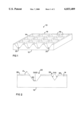
- FIG. 1 is a perspective view of a semiconductor substrate according to one embodiment of the invention.
- FIG. 2 is a side cross-sectional view showing two different types of recesses that can be used to form a semiconductor substrate.
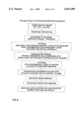
- FIG. 3 is a flow diagram illustrating a process flow suitable for use in manufacturing a semiconductor substrate according to one embodiment of the invention.
- semiconductor substrate 10 includes a planar front surface 12 on which a plurality of active devices will be formed (forming semiconductor dies), a planar back surface 14, and an array 16 of recesses 18 extending into the substrate from the back surface 14.
- the array 16 is comprised of substantially straight rows and columns, so that the backside of the substrate has a substantially uniform distribution of recesses.
- the recesses are preferably dimensioned so that there will be several recesses on the backside of each die. For certain die sizes, it is preferred that the recess array be aligned with respect to the die pattern on the front surface 12. This arrangement allows the substrate 10 to be sliced into dies that would be consistent for subsequent processing.
- the recesses 18 do not extend all the way through the substrate 10. Instead, a predetermined thickness of substrate 10 remains beneath the floor 20 of recesses 18. Preferably, this predetermined thickness is from about 25 to 100 microns. Thus, the minimum thickness of the substrate 10 is this predetermined thickness at the floors of the recesses, and the thickness of the substrate is greater in all other areas of the substrate. This structure provides a structurally robust substrate that can easily withstand the forces that are typically encountered during processing.
- the recesses can have various geometries, for example truncated pyramidal recess 22 and pyramidal recess 24.
- the manner in which these various shapes can be formed will be described in further detail below.
- the angle A between the planar back surface 14 and the wall 16 of the recess is from about 40 to 90 degrees, more preferably about 55 degrees, as shown.
- FIG. 3 A preferred process flow for manufacturing the substrate 10 is shown in FIG. 3.
- the planar front surface 12 of the substrate 10 is protected, e.g., by tape, a photoresist or any other suitable protection.
- the back surface of the substrate is ground to a predetermined thickness, preferably the minimum manufacturable thickness (i.e., the minimum thickness at which the substrate, without the recesses, can be handled without breakage), to form the planar back surface 14.
- the minimum manufacturable thickness is generally about 175 to 250 microns.
- an intermediate material that is resistant to the etchant may need to be applied to back surface 14. Suitable intermediate materials include silicon dioxide and nitride.
- the planar back surface 14 is patterned using conventional methods, e.g., photolithography, to mask a grid pattern and leave exposed "islands" where the recesses are to be formed (see mask layer 26 in FIG. 2). If an intermediate material was applied beneath the patterning material, it is now removed from the "islands” using a suitable etchant.
- the back surface 14 is etched to remove substrate material from the "island" areas that are not covered by the mask layer and thereby form the recesses 18. After the recesses have been formed, the mask is removed, the front planar surface protection is removed, and a highly conductive material is deposited on the planar back surface.
- the different geometries shown in FIG. 2 can be formed by masking the planar back surface 14 and etching with an orientation-dependent chemical anisotropic silicon etchant, for example a mixture of KOH, normal propanol and water.
- an orientation-dependent chemical anisotropic silicon etchant for example a mixture of KOH, normal propanol and water.
- anisotropic etching of silicon are well known, and are described, e.g., in "Anisotropic Etching of Silicon", Kenneth E. Bean, IEEE Transactions on Electron Devices, Vol. ED-25, no. 10, October, 1978.
- Preferred anisotropic silicon etchants have a much slower etch rate on the (111) plane of the silicon relative to the (100) plane. As a result, by masking the (100) plane, uniformly shaped recesses can be etched into the silicon.
- the difference in geometry of recesses 22 and 24 is a result of the shape of the "island” area that is not masked and the etch time.
- the "island” area is smaller for recess 24, and thus the recess "bottomed out” in the V-shaped cross-section in the same amount of etch time that it took to form the flat-bottomed recess 22. (If etching had continued, recess 22 would eventually also have bottomed out in a V-shaped cross-section having a greater depth.)
- different geometries can be readily obtained by varying the etchant used, the mask pattern, and the etch time.
Abstract
Description
Claims (8)
Priority Applications (1)
| Application Number | Priority Date | Filing Date | Title |
|---|---|---|---|
| US09/086,654 US6033489A (en) | 1998-05-29 | 1998-05-29 | Semiconductor substrate and method of making same |
Applications Claiming Priority (1)
| Application Number | Priority Date | Filing Date | Title |
|---|---|---|---|
| US09/086,654 US6033489A (en) | 1998-05-29 | 1998-05-29 | Semiconductor substrate and method of making same |
Publications (1)
| Publication Number | Publication Date |
|---|---|
| US6033489A true US6033489A (en) | 2000-03-07 |
Family
ID=22200001
Family Applications (1)
| Application Number | Title | Priority Date | Filing Date |
|---|---|---|---|
| US09/086,654 Expired - Lifetime US6033489A (en) | 1998-05-29 | 1998-05-29 | Semiconductor substrate and method of making same |
Country Status (1)
| Country | Link |
|---|---|
| US (1) | US6033489A (en) |
Cited By (11)
| Publication number | Priority date | Publication date | Assignee | Title |
|---|---|---|---|---|
| US6541753B2 (en) * | 1998-11-02 | 2003-04-01 | Hammatsu Photonics K.K. | Semiconductor energy detector having reinforcement |
| US20060022263A1 (en) * | 2004-07-30 | 2006-02-02 | International Rectifier Corporation | Selective substrate thinning for power mosgated devices |
| US20070020884A1 (en) * | 2005-07-25 | 2007-01-25 | Qi Wang | Semiconductor structures formed on substrates and methods of manufacturing the same |
| US20090107545A1 (en) * | 2006-10-09 | 2009-04-30 | Soltaix, Inc. | Template for pyramidal three-dimensional thin-film solar cell manufacturing and methods of use |
| US20090181520A1 (en) * | 2007-10-01 | 2009-07-16 | Minhua Li | Method and Structure for Dividing a Substrate into Individual Devices |
| US20090179259A1 (en) * | 2007-09-27 | 2009-07-16 | Qi Wang | Semiconductor device with (110)-oriented silicon |
| US20090273082A1 (en) * | 2008-05-05 | 2009-11-05 | Suku Kim | Methods and designs for localized wafer thinning |
| US20100059797A1 (en) * | 2008-09-09 | 2010-03-11 | Tat Ngai | (110)-oriented p-channel trench mosfet having high-k gate dielectric |
| US20100123225A1 (en) * | 2008-11-20 | 2010-05-20 | Gruenhagen Michael D | Semiconductor Die Structures for Wafer-Level Chipscale Packaging of Power Devices, Packages and Systems for Using the Same, and Methods of Making the Same |
| US20100148325A1 (en) * | 2008-12-12 | 2010-06-17 | Gruenhagen Michael D | Semiconductor Dice with Backside Trenches Filled With Elastic Material For Improved Attachment, Packages Using the Same, and Methods of Making the Same |
| US10074611B1 (en) | 2017-03-08 | 2018-09-11 | Semiconductor Components Industries, Llc | Semiconductor device and method of forming backside openings for an ultra-thin semiconductor die |
Citations (22)
| Publication number | Priority date | Publication date | Assignee | Title |
|---|---|---|---|---|
| US3428499A (en) * | 1965-01-01 | 1969-02-18 | Int Standard Electric Corp | Semiconductor process including reduction of the substrate thickness |
| US4169008A (en) * | 1977-06-13 | 1979-09-25 | International Business Machines Corporation | Process for producing uniform nozzle orifices in silicon wafers |
| US4266334A (en) * | 1979-07-25 | 1981-05-12 | Rca Corporation | Manufacture of thinned substrate imagers |
| US4470875A (en) * | 1983-11-09 | 1984-09-11 | At&T Bell Laboratories | Fabrication of silicon devices requiring anisotropic etching |
| US4525924A (en) * | 1978-12-23 | 1985-07-02 | Semikron Gesellschaft Fur Gleichrichterbau Und Elektronik | Method for producing a plurality of semiconductor circuits |
| US4539050A (en) * | 1982-12-15 | 1985-09-03 | Wacker-Chemitronic Gesellschaft Fur Elektronik-Grundstoffe M.B.H. | Process for the manufacture of semiconductor wafers with a rear side having a gettering action |
| US4559086A (en) * | 1984-07-02 | 1985-12-17 | Eastman Kodak Company | Backside gettering of silicon wafers utilizing selectively annealed single crystal silicon portions disposed between and extending into polysilicon portions |
| US4597166A (en) * | 1982-02-10 | 1986-07-01 | Tokyo Shibaura Denki Kabushiki Kaisha | Semiconductor substrate and method for manufacturing semiconductor device using the same |
| US4604161A (en) * | 1985-05-02 | 1986-08-05 | Xerox Corporation | Method of fabricating image sensor arrays |
| US4822755A (en) * | 1988-04-25 | 1989-04-18 | Xerox Corporation | Method of fabricating large area semiconductor arrays |
| US4863560A (en) * | 1988-08-22 | 1989-09-05 | Xerox Corp | Fabrication of silicon structures by single side, multiple step etching process |
| US5034068A (en) * | 1990-02-23 | 1991-07-23 | Spectrolab, Inc. | Photovoltaic cell having structurally supporting open conductive back electrode structure, and method of fabricating the cell |
| US5164804A (en) * | 1990-09-18 | 1992-11-17 | Mitsubishi Denki Kabushiki Kaisha | Semiconductor device having high breakdown voltage and low resistance and method of fabricating the same |
| US5166097A (en) * | 1990-11-26 | 1992-11-24 | The Boeing Company | Silicon wafers containing conductive feedthroughs |
| US5264378A (en) * | 1990-04-20 | 1993-11-23 | Fuji Electric Co., Ltd. | Method for making a conductivity modulation MOSFET |
| US5523174A (en) * | 1993-05-07 | 1996-06-04 | Ibiden Co., Ltd. | Printed circuit boards |
| US5635762A (en) * | 1993-05-18 | 1997-06-03 | U.S. Philips Corporation | Flip chip semiconductor device with dual purpose metallized ground conductor |
| US5800631A (en) * | 1995-08-24 | 1998-09-01 | Canon Kabushiki Kaisha | Solar cell module having a specific back side covering material and a process for the production of said solar cell module |
| US5804847A (en) * | 1994-07-14 | 1998-09-08 | The United States Of America As Represented By The Secretary Of The Air Force | Backside illuminated FET optical receiver with gallium arsenide species |
| US5840593A (en) * | 1992-04-08 | 1998-11-24 | Elm Technology Corporation | Membrane dielectric isolation IC fabrication |
| US5913713A (en) * | 1997-07-31 | 1999-06-22 | International Business Machines Corporation | CMP polishing pad backside modifications for advantageous polishing results |
| US5962081A (en) * | 1995-06-21 | 1999-10-05 | Pharmacia Biotech Ab | Method for the manufacture of a membrane-containing microstructure |
-
1998
- 1998-05-29 US US09/086,654 patent/US6033489A/en not_active Expired - Lifetime
Patent Citations (22)
| Publication number | Priority date | Publication date | Assignee | Title |
|---|---|---|---|---|
| US3428499A (en) * | 1965-01-01 | 1969-02-18 | Int Standard Electric Corp | Semiconductor process including reduction of the substrate thickness |
| US4169008A (en) * | 1977-06-13 | 1979-09-25 | International Business Machines Corporation | Process for producing uniform nozzle orifices in silicon wafers |
| US4525924A (en) * | 1978-12-23 | 1985-07-02 | Semikron Gesellschaft Fur Gleichrichterbau Und Elektronik | Method for producing a plurality of semiconductor circuits |
| US4266334A (en) * | 1979-07-25 | 1981-05-12 | Rca Corporation | Manufacture of thinned substrate imagers |
| US4597166A (en) * | 1982-02-10 | 1986-07-01 | Tokyo Shibaura Denki Kabushiki Kaisha | Semiconductor substrate and method for manufacturing semiconductor device using the same |
| US4539050A (en) * | 1982-12-15 | 1985-09-03 | Wacker-Chemitronic Gesellschaft Fur Elektronik-Grundstoffe M.B.H. | Process for the manufacture of semiconductor wafers with a rear side having a gettering action |
| US4470875A (en) * | 1983-11-09 | 1984-09-11 | At&T Bell Laboratories | Fabrication of silicon devices requiring anisotropic etching |
| US4559086A (en) * | 1984-07-02 | 1985-12-17 | Eastman Kodak Company | Backside gettering of silicon wafers utilizing selectively annealed single crystal silicon portions disposed between and extending into polysilicon portions |
| US4604161A (en) * | 1985-05-02 | 1986-08-05 | Xerox Corporation | Method of fabricating image sensor arrays |
| US4822755A (en) * | 1988-04-25 | 1989-04-18 | Xerox Corporation | Method of fabricating large area semiconductor arrays |
| US4863560A (en) * | 1988-08-22 | 1989-09-05 | Xerox Corp | Fabrication of silicon structures by single side, multiple step etching process |
| US5034068A (en) * | 1990-02-23 | 1991-07-23 | Spectrolab, Inc. | Photovoltaic cell having structurally supporting open conductive back electrode structure, and method of fabricating the cell |
| US5264378A (en) * | 1990-04-20 | 1993-11-23 | Fuji Electric Co., Ltd. | Method for making a conductivity modulation MOSFET |
| US5164804A (en) * | 1990-09-18 | 1992-11-17 | Mitsubishi Denki Kabushiki Kaisha | Semiconductor device having high breakdown voltage and low resistance and method of fabricating the same |
| US5166097A (en) * | 1990-11-26 | 1992-11-24 | The Boeing Company | Silicon wafers containing conductive feedthroughs |
| US5840593A (en) * | 1992-04-08 | 1998-11-24 | Elm Technology Corporation | Membrane dielectric isolation IC fabrication |
| US5523174A (en) * | 1993-05-07 | 1996-06-04 | Ibiden Co., Ltd. | Printed circuit boards |
| US5635762A (en) * | 1993-05-18 | 1997-06-03 | U.S. Philips Corporation | Flip chip semiconductor device with dual purpose metallized ground conductor |
| US5804847A (en) * | 1994-07-14 | 1998-09-08 | The United States Of America As Represented By The Secretary Of The Air Force | Backside illuminated FET optical receiver with gallium arsenide species |
| US5962081A (en) * | 1995-06-21 | 1999-10-05 | Pharmacia Biotech Ab | Method for the manufacture of a membrane-containing microstructure |
| US5800631A (en) * | 1995-08-24 | 1998-09-01 | Canon Kabushiki Kaisha | Solar cell module having a specific back side covering material and a process for the production of said solar cell module |
| US5913713A (en) * | 1997-07-31 | 1999-06-22 | International Business Machines Corporation | CMP polishing pad backside modifications for advantageous polishing results |
Non-Patent Citations (4)
| Title |
|---|
| Kenneth Bean, "Anisotropic Etching of Silicon", IEEE Transactions on Electron Devices, Oct. 19, 1978, pp. 1185-1193. |
| Kenneth Bean, Anisotropic Etching of Silicon , IEEE Transactions on Electron Devices , Oct. 19, 1978, pp. 1185 1193. * |
| S. Wolf and R.N. Tauber, Silicon Processing for the VLSI Era, vol. 1 Process Technology , Lattice Press, Sunset Beach, CA, 1986, pp. 531 532. * |
| S. Wolf and R.N. Tauber, Silicon Processing for the VLSI Era, vol. 1--Process Technology, Lattice Press, Sunset Beach, CA, 1986, pp. 531-532. |
Cited By (27)
| Publication number | Priority date | Publication date | Assignee | Title |
|---|---|---|---|---|
| US6541753B2 (en) * | 1998-11-02 | 2003-04-01 | Hammatsu Photonics K.K. | Semiconductor energy detector having reinforcement |
| US20060022263A1 (en) * | 2004-07-30 | 2006-02-02 | International Rectifier Corporation | Selective substrate thinning for power mosgated devices |
| US20070020884A1 (en) * | 2005-07-25 | 2007-01-25 | Qi Wang | Semiconductor structures formed on substrates and methods of manufacturing the same |
| US7635637B2 (en) | 2005-07-25 | 2009-12-22 | Fairchild Semiconductor Corporation | Semiconductor structures formed on substrates and methods of manufacturing the same |
| US20100052046A1 (en) * | 2005-07-25 | 2010-03-04 | Fairchild Semiconductor Corporation | Semiconductor structures formed on substrates and methods of manufacturing the same |
| US20090107545A1 (en) * | 2006-10-09 | 2009-04-30 | Soltaix, Inc. | Template for pyramidal three-dimensional thin-film solar cell manufacturing and methods of use |
| US8338886B2 (en) | 2007-09-27 | 2012-12-25 | Fairchild Semiconductor Corporation | Semiconductor device with (110)-oriented silicon |
| US20090179259A1 (en) * | 2007-09-27 | 2009-07-16 | Qi Wang | Semiconductor device with (110)-oriented silicon |
| US8101500B2 (en) | 2007-09-27 | 2012-01-24 | Fairchild Semiconductor Corporation | Semiconductor device with (110)-oriented silicon |
| US7951688B2 (en) | 2007-10-01 | 2011-05-31 | Fairchild Semiconductor Corporation | Method and structure for dividing a substrate into individual devices |
| US8343852B2 (en) | 2007-10-01 | 2013-01-01 | Fairchild Semiconductor Corporation | Method and structure for dividing a substrate into individual devices |
| US20090181520A1 (en) * | 2007-10-01 | 2009-07-16 | Minhua Li | Method and Structure for Dividing a Substrate into Individual Devices |
| US20110201179A1 (en) * | 2007-10-01 | 2011-08-18 | Minhua Li | Method and structure for dividing a substrate into individual devices |
| US20090273082A1 (en) * | 2008-05-05 | 2009-11-05 | Suku Kim | Methods and designs for localized wafer thinning |
| US8624393B2 (en) * | 2008-05-05 | 2014-01-07 | Fairchild Semiconductor Corporation | Methods and designs for localized wafer thinning |
| US20120168947A1 (en) * | 2008-05-05 | 2012-07-05 | Suku Kim | Methods and Designs for Localized Wafer Thinning |
| US8158506B2 (en) * | 2008-05-05 | 2012-04-17 | Fairchild Semiconductor Corporation | Methods and designs for localized wafer thinning |
| US8039877B2 (en) | 2008-09-09 | 2011-10-18 | Fairchild Semiconductor Corporation | (110)-oriented p-channel trench MOSFET having high-K gate dielectric |
| US20100059797A1 (en) * | 2008-09-09 | 2010-03-11 | Tat Ngai | (110)-oriented p-channel trench mosfet having high-k gate dielectric |
| US8058732B2 (en) | 2008-11-20 | 2011-11-15 | Fairchild Semiconductor Corporation | Semiconductor die structures for wafer-level chipscale packaging of power devices, packages and systems for using the same, and methods of making the same |
| US20100123225A1 (en) * | 2008-11-20 | 2010-05-20 | Gruenhagen Michael D | Semiconductor Die Structures for Wafer-Level Chipscale Packaging of Power Devices, Packages and Systems for Using the Same, and Methods of Making the Same |
| US7960800B2 (en) | 2008-12-12 | 2011-06-14 | Fairchild Semiconductor Corporation | Semiconductor dice with backside trenches filled with elastic material for improved attachment, packages using the same, and methods of making the same |
| US20110230046A1 (en) * | 2008-12-12 | 2011-09-22 | Gruenhagen Michael D | Semiconductor dice with backside trenches filled with elastic material for improved attachment, packages using the same, and methods of making the same |
| US20100148325A1 (en) * | 2008-12-12 | 2010-06-17 | Gruenhagen Michael D | Semiconductor Dice with Backside Trenches Filled With Elastic Material For Improved Attachment, Packages Using the Same, and Methods of Making the Same |
| US8598035B2 (en) | 2008-12-12 | 2013-12-03 | Fairchild Semiconductor Corporation | Semiconductor dice with backside trenches filled with elastic material for improved attachment, packages using the same, and methods of making the same |
| US10074611B1 (en) | 2017-03-08 | 2018-09-11 | Semiconductor Components Industries, Llc | Semiconductor device and method of forming backside openings for an ultra-thin semiconductor die |
| US10727188B2 (en) | 2017-03-08 | 2020-07-28 | Semiconductor Components Industries, Llc | Semiconductor device and method of forming backside openings for an ultra-thin semiconductor die |
Similar Documents
| Publication | Publication Date | Title |
|---|---|---|
| EP0328281B1 (en) | Directable aperture etched in silicon | |
| US6960510B2 (en) | Method of making sub-lithographic features | |
| US4863560A (en) | Fabrication of silicon structures by single side, multiple step etching process | |
| EP1345275B1 (en) | Method for roughening semiconductor surface | |
| US6033489A (en) | Semiconductor substrate and method of making same | |
| KR970007494A (en) | Method for manufacturing a sub-lithographic etching mask | |
| EP1235264A3 (en) | Direct etch for thin film resistor using a hard mask | |
| WO2000001010A3 (en) | Method for producing semiconductor components | |
| KR970013074A (en) | Planarization method of semiconductor device and device isolation method using same | |
| US5282926A (en) | Method of anisotropically etching monocrystalline, disk-shaped wafers | |
| EP0875928A3 (en) | Metallization in semiconductor devices | |
| US6968617B2 (en) | Methods of fabricating fluid ejection devices | |
| JP2973423B2 (en) | Superconducting element and manufacturing method thereof | |
| US5068207A (en) | Method for producing a planar surface in integrated circuit manufacturing | |
| US5640038A (en) | Integrated circuit structure with self-planarized layers | |
| JPH07326621A (en) | Minute pattern forming method for semiconductor element | |
| JP3923136B2 (en) | Semiconductor device and manufacturing method thereof | |
| JPH07106327A (en) | Semiconductor device and its manufacture | |
| KR100370137B1 (en) | A array of flat rom cell method for fabricating the same | |
| KR970006929B1 (en) | Preparation process of metal wiring of semiconductor devices | |
| JPS58184764A (en) | Integrated circuit device | |
| US5618753A (en) | Method for forming electrodes on mesa structures of a semiconductor substrate | |
| US4693783A (en) | Method of producing interconnections in a semiconductor integrated circuit structure | |
| JPS6420641A (en) | Manufacture of semiconductor device | |
| KR100197657B1 (en) | Method of manufacturing fine contact hole in semiconductor device |
Legal Events
| Date | Code | Title | Description |
|---|---|---|---|
| AS | Assignment |
Owner name: FAIRCHILD SEMICONDUCTOR CORP., MAINE Free format text: ASSIGNMENT OF ASSIGNORS INTEREST;ASSIGNORS:MARCHANT, BRUCE D.;SAPP, STEVEN;WELCH, THOMAS;REEL/FRAME:009203/0369;SIGNING DATES FROM 19980427 TO 19980526 |
|
| AS | Assignment |
Owner name: CREDIT SUISSE FIRST BOSTON, NEW YORK Free format text: SECURITY AGREEMENT;ASSIGNOR:FAIRCHILD SEMICONDUCTOR CORPORATION;REEL/FRAME:009883/0800 Effective date: 19990414 |
|
| AS | Assignment |
Owner name: FAIRCHILD SEMICONDUCTOR CORPORATION, MAINE Free format text: RELEASE BY SECURED PARTY;ASSIGNOR:BANKERS TRUST COMPANY;REEL/FRAME:009901/0528 Effective date: 19990414 |
|
| STCF | Information on status: patent grant |
Free format text: PATENTED CASE |
|
| AS | Assignment |
Owner name: FAIRCHILD SEMICONDUCTOR CORPORATION, MAINE Free format text: RELEASE;ASSIGNOR:CREDIT SUISSE FIRST BOSTON;REEL/FRAME:010996/0537 Effective date: 20000602 |
|
| FEPP | Fee payment procedure |
Free format text: PAYOR NUMBER ASSIGNED (ORIGINAL EVENT CODE: ASPN); ENTITY STATUS OF PATENT OWNER: LARGE ENTITY |
|
| FPAY | Fee payment |
Year of fee payment: 4 |
|
| FEPP | Fee payment procedure |
Free format text: PAYER NUMBER DE-ASSIGNED (ORIGINAL EVENT CODE: RMPN); ENTITY STATUS OF PATENT OWNER: LARGE ENTITY |
|
| FPAY | Fee payment |
Year of fee payment: 8 |
|
| REMI | Maintenance fee reminder mailed | ||
| FPAY | Fee payment |
Year of fee payment: 12 |
|
| AS | Assignment |
Owner name: FAIRCHILD SEMICONDUCTOR CORPORATION, MAINE Free format text: CORRECTIVE ASSIGNMENT TO CORRECT THE NAME OF THE RECEIVING PARTY PREVIOUSLY RECORDED AT REEL: 009203 FRAME: 0369. ASSIGNOR(S) HEREBY CONFIRMS THE ASSIGNMENT;ASSIGNORS:MARCHANT, BRUCE D;SAPP, STEVEN;WELCH, THOMAS;SIGNING DATES FROM 19980427 TO 19980526;REEL/FRAME:039429/0034 |
|
| AS | Assignment |
Owner name: DEUTSCHE BANK AG NEW YORK BRANCH, AS COLLATERAL AGENT, NEW YORK Free format text: PATENT SECURITY AGREEMENT;ASSIGNOR:FAIRCHILD SEMICONDUCTOR CORPORATION;REEL/FRAME:040075/0644 Effective date: 20160916 Owner name: DEUTSCHE BANK AG NEW YORK BRANCH, AS COLLATERAL AG Free format text: PATENT SECURITY AGREEMENT;ASSIGNOR:FAIRCHILD SEMICONDUCTOR CORPORATION;REEL/FRAME:040075/0644 Effective date: 20160916 |
|
| AS | Assignment |
Owner name: SEMICONDUCTOR COMPONENTS INDUSTRIES, LLC, ARIZONA Free format text: ASSIGNMENT OF ASSIGNORS INTEREST;ASSIGNOR:FAIRCHILD SEMICONDUCTOR CORPORATION;REEL/FRAME:057694/0374 Effective date: 20210722 |
|
| AS | Assignment |
Owner name: FAIRCHILD SEMICONDUCTOR CORPORATION, ARIZONA Free format text: RELEASE BY SECURED PARTY;ASSIGNOR:DEUTSCHE BANK AG NEW YORK BRANCH;REEL/FRAME:057969/0206 Effective date: 20211027 |
|
| AS | Assignment |
Owner name: DEUTSCHE BANK AG NEW YORK BRANCH, AS COLLATERAL AGENT, NEW YORK Free format text: SECURITY INTEREST;ASSIGNOR:SEMICONDUCTOR COMPONENTS INDUSTRIES, LLC;REEL/FRAME:058871/0799 Effective date: 20211028 |
|
| AS | Assignment |
Owner name: FAIRCHILD SEMICONDUCTOR CORPORATION, ARIZONA Free format text: RELEASE OF SECURITY INTEREST IN PATENTS RECORDED AT REEL 040075, FRAME 0644;ASSIGNOR:DEUTSCHE BANK AG NEW YORK BRANCH, AS COLLATERAL AGENT;REEL/FRAME:064070/0536 Effective date: 20230622 Owner name: SEMICONDUCTOR COMPONENTS INDUSTRIES, LLC, ARIZONA Free format text: RELEASE OF SECURITY INTEREST IN PATENTS RECORDED AT REEL 040075, FRAME 0644;ASSIGNOR:DEUTSCHE BANK AG NEW YORK BRANCH, AS COLLATERAL AGENT;REEL/FRAME:064070/0536 Effective date: 20230622 |
|
| AS | Assignment |
Owner name: FAIRCHILD SEMICONDUCTOR CORPORATION, ARIZONA Free format text: RELEASE OF SECURITY INTEREST IN PATENTS RECORDED AT REEL 058871, FRAME 0799;ASSIGNOR:DEUTSCHE BANK AG NEW YORK BRANCH, AS COLLATERAL AGENT;REEL/FRAME:065653/0001 Effective date: 20230622 Owner name: SEMICONDUCTOR COMPONENTS INDUSTRIES, LLC, ARIZONA Free format text: RELEASE OF SECURITY INTEREST IN PATENTS RECORDED AT REEL 058871, FRAME 0799;ASSIGNOR:DEUTSCHE BANK AG NEW YORK BRANCH, AS COLLATERAL AGENT;REEL/FRAME:065653/0001 Effective date: 20230622 |