US6033491A - Fabrication process of Ni-Mn spin valve sensor - Google Patents
Fabrication process of Ni-Mn spin valve sensor Download PDFInfo
- Publication number
- US6033491A US6033491A US08/922,963 US92296397A US6033491A US 6033491 A US6033491 A US 6033491A US 92296397 A US92296397 A US 92296397A US 6033491 A US6033491 A US 6033491A
- Authority
- US
- United States
- Prior art keywords
- layer
- pinned
- afm
- manufacturing
- layers
- Prior art date
- Legal status (The legal status is an assumption and is not a legal conclusion. Google has not performed a legal analysis and makes no representation as to the accuracy of the status listed.)
- Expired - Fee Related
Links
Images

Classifications
-
- B—PERFORMING OPERATIONS; TRANSPORTING
- B82—NANOTECHNOLOGY
- B82Y—SPECIFIC USES OR APPLICATIONS OF NANOSTRUCTURES; MEASUREMENT OR ANALYSIS OF NANOSTRUCTURES; MANUFACTURE OR TREATMENT OF NANOSTRUCTURES
- B82Y25/00—Nanomagnetism, e.g. magnetoimpedance, anisotropic magnetoresistance, giant magnetoresistance or tunneling magnetoresistance
-
- B—PERFORMING OPERATIONS; TRANSPORTING
- B82—NANOTECHNOLOGY
- B82Y—SPECIFIC USES OR APPLICATIONS OF NANOSTRUCTURES; MEASUREMENT OR ANALYSIS OF NANOSTRUCTURES; MANUFACTURE OR TREATMENT OF NANOSTRUCTURES
- B82Y10/00—Nanotechnology for information processing, storage or transmission, e.g. quantum computing or single electron logic
-
- G—PHYSICS
- G01—MEASURING; TESTING
- G01R—MEASURING ELECTRIC VARIABLES; MEASURING MAGNETIC VARIABLES
- G01R33/00—Arrangements or instruments for measuring magnetic variables
- G01R33/02—Measuring direction or magnitude of magnetic fields or magnetic flux
- G01R33/06—Measuring direction or magnitude of magnetic fields or magnetic flux using galvano-magnetic devices
- G01R33/09—Magnetoresistive devices
- G01R33/093—Magnetoresistive devices using multilayer structures, e.g. giant magnetoresistance sensors
-
- G—PHYSICS
- G11—INFORMATION STORAGE
- G11B—INFORMATION STORAGE BASED ON RELATIVE MOVEMENT BETWEEN RECORD CARRIER AND TRANSDUCER
- G11B5/00—Recording by magnetisation or demagnetisation of a record carrier; Reproducing by magnetic means; Record carriers therefor
- G11B5/127—Structure or manufacture of heads, e.g. inductive
- G11B5/33—Structure or manufacture of flux-sensitive heads, i.e. for reproduction only; Combination of such heads with means for recording or erasing only
- G11B5/39—Structure or manufacture of flux-sensitive heads, i.e. for reproduction only; Combination of such heads with means for recording or erasing only using magneto-resistive devices or effects
- G11B5/3903—Structure or manufacture of flux-sensitive heads, i.e. for reproduction only; Combination of such heads with means for recording or erasing only using magneto-resistive devices or effects using magnetic thin film layers or their effects, the films being part of integrated structures
- G11B5/3906—Details related to the use of magnetic thin film layers or to their effects
- G11B5/3929—Disposition of magnetic thin films not used for directly coupling magnetic flux from the track to the MR film or for shielding
- G11B5/3932—Magnetic biasing films
-
- H—ELECTRICITY
- H01—ELECTRIC ELEMENTS
- H01F—MAGNETS; INDUCTANCES; TRANSFORMERS; SELECTION OF MATERIALS FOR THEIR MAGNETIC PROPERTIES
- H01F10/00—Thin magnetic films, e.g. of one-domain structure
- H01F10/32—Spin-exchange-coupled multilayers, e.g. nanostructured superlattices
- H01F10/324—Exchange coupling of magnetic film pairs via a very thin non-magnetic spacer, e.g. by exchange with conduction electrons of the spacer
- H01F10/3268—Exchange coupling of magnetic film pairs via a very thin non-magnetic spacer, e.g. by exchange with conduction electrons of the spacer the exchange coupling being asymmetric, e.g. by use of additional pinning, by using antiferromagnetic or ferromagnetic coupling interface, i.e. so-called spin-valve [SV] structure, e.g. NiFe/Cu/NiFe/FeMn
-
- H—ELECTRICITY
- H01—ELECTRIC ELEMENTS
- H01F—MAGNETS; INDUCTANCES; TRANSFORMERS; SELECTION OF MATERIALS FOR THEIR MAGNETIC PROPERTIES
- H01F41/00—Apparatus or processes specially adapted for manufacturing or assembling magnets, inductances or transformers; Apparatus or processes specially adapted for manufacturing materials characterised by their magnetic properties
- H01F41/14—Apparatus or processes specially adapted for manufacturing or assembling magnets, inductances or transformers; Apparatus or processes specially adapted for manufacturing materials characterised by their magnetic properties for applying magnetic films to substrates
- H01F41/30—Apparatus or processes specially adapted for manufacturing or assembling magnets, inductances or transformers; Apparatus or processes specially adapted for manufacturing materials characterised by their magnetic properties for applying magnetic films to substrates for applying nanostructures, e.g. by molecular beam epitaxy [MBE]
- H01F41/302—Apparatus or processes specially adapted for manufacturing or assembling magnets, inductances or transformers; Apparatus or processes specially adapted for manufacturing materials characterised by their magnetic properties for applying magnetic films to substrates for applying nanostructures, e.g. by molecular beam epitaxy [MBE] for applying spin-exchange-coupled multilayers, e.g. nanostructured superlattices
-
- G—PHYSICS
- G11—INFORMATION STORAGE
- G11B—INFORMATION STORAGE BASED ON RELATIVE MOVEMENT BETWEEN RECORD CARRIER AND TRANSDUCER
- G11B5/00—Recording by magnetisation or demagnetisation of a record carrier; Reproducing by magnetic means; Record carriers therefor
- G11B5/127—Structure or manufacture of heads, e.g. inductive
- G11B5/33—Structure or manufacture of flux-sensitive heads, i.e. for reproduction only; Combination of such heads with means for recording or erasing only
- G11B5/39—Structure or manufacture of flux-sensitive heads, i.e. for reproduction only; Combination of such heads with means for recording or erasing only using magneto-resistive devices or effects
- G11B2005/3996—Structure or manufacture of flux-sensitive heads, i.e. for reproduction only; Combination of such heads with means for recording or erasing only using magneto-resistive devices or effects large or giant magnetoresistive effects [GMR], e.g. as generated in spin-valve [SV] devices
-
- G—PHYSICS
- G11—INFORMATION STORAGE
- G11B—INFORMATION STORAGE BASED ON RELATIVE MOVEMENT BETWEEN RECORD CARRIER AND TRANSDUCER
- G11B5/00—Recording by magnetisation or demagnetisation of a record carrier; Reproducing by magnetic means; Record carriers therefor
- G11B5/127—Structure or manufacture of heads, e.g. inductive
- G11B5/31—Structure or manufacture of heads, e.g. inductive using thin films
- G11B5/3163—Fabrication methods or processes specially adapted for a particular head structure, e.g. using base layers for electroplating, using functional layers for masking, using energy or particle beams for shaping the structure or modifying the properties of the basic layers
-
- Y—GENERAL TAGGING OF NEW TECHNOLOGICAL DEVELOPMENTS; GENERAL TAGGING OF CROSS-SECTIONAL TECHNOLOGIES SPANNING OVER SEVERAL SECTIONS OF THE IPC; TECHNICAL SUBJECTS COVERED BY FORMER USPC CROSS-REFERENCE ART COLLECTIONS [XRACs] AND DIGESTS
- Y10—TECHNICAL SUBJECTS COVERED BY FORMER USPC
- Y10T—TECHNICAL SUBJECTS COVERED BY FORMER US CLASSIFICATION
- Y10T29/00—Metal working
- Y10T29/49—Method of mechanical manufacture
- Y10T29/49002—Electrical device making
- Y10T29/4902—Electromagnet, transformer or inductor
- Y10T29/49021—Magnetic recording reproducing transducer [e.g., tape head, core, etc.]
- Y10T29/49032—Fabricating head structure or component thereof
- Y10T29/49034—Treating to affect magnetic properties
Definitions
- This invention relates generally to magnetic transducers for reading information signals from a magnetic medium and, in particular, to an improved process for fabrication of a spin valve magnetoresistive read sensor.
- Computers often include auxiliary memory storage devices having media on which data can be written and from which data can be read for later use.
- a direct access storage device disk drive
- rotating magnetic disks are commonly used for storing data in magnetic form on the disk surfaces. Data is recorded on concentric, radially spaced tracks on the disk surfaces. Magnetic heads including read sensors are then used to read data from the tracks on the disk surfaces.
- magnetoresistive read sensors In high capacity disk drives, magnetoresistive read sensors, commonly referred to as MR heads, are the prevailing read sensors because of their capability to read data from a surface of a disk at greater linear densities than thin film inductive heads.
- An MR sensor detects a magnetic field through the change in the resistance of its MR sensing layer (also referred to as an "MR element") as a function of the strength and direction of the magnetic flux being sensed by the MR layer.
- GMR giant magnetoresistive
- the resistance of the MR sensing layer varies as a function of the spin-dependent transmission of the conduction electrons between the magnetic layers separated by a non-magnetic layer (spacer) and the accompanying spin-dependent scattering which takes place at the interface of the magnetic and non-magnetic layers and within the magnetic layers.
- GMR sensors using only two layers of ferromagnetic material e.g., Ni-Fe or Co or Ni-Fe/Co
- ferromagnetic material e.g., Ni-Fe or Co or Ni-Fe/Co
- non-magnetic metallic material e.g., copper
- spin valve (SV) sensors manifesting the SV effect.
- one of the ferromagnetic layers referred to as the pinned layer, has its magnetization typically pinned by exchange coupling with an antiferromagnetic (e.g., Fe-Mn or NiO) layer.
- an antiferromagnetic e.g., Fe-Mn or NiO
- the pinning field generated by the antiferromagnetic layer should be greater than demagnetizing fields (about 200 Oe) at the operating temperature of the SV sensor (about 120° C.) to ensure that the magnetization direction of the pinned layer remains fixed during the application of external fields (e.g., fields from bits recorded on the disk).
- demagnetizing fields about 200 Oe
- the magnetization of the other ferromagnetic layer referred to as the free layer, however, is not fixed and is free to rotate in response to the field from the disk.
- the SV effect i.e., the net change in resistance, exhibited by a typical prior art SV sensor with Ni-Fe free and pinned layers is about 3% to 4%.
- FIG. 1 shows a prior art SV sensor 100 comprising end regions 104 and 106 separated by a central region 102.
- a free layer 110 is separated from a pinned layer 120 by a non-magnetic, electrically-conducting spacer layer 115.
- the magnetization of the pinned layer 120 is fixed by an antiferromagnetic (AFM) layer 125 in a transverse direction (perpendicular to an air bearing surface).
- AFM antiferromagnetic
- Free layer 110, spacer layer 115, pinned layer 120 and the AFM layer 125 are all formed in the central region 102.
- Sensing means 170 connected to leads 140 and 145 sense the change in the resistance due to changes induced in the free layer 110 by the external magnetic field (e.g., field generated by a data bit stored on a disk).
- the magnetization of the pinned layer 120 in the prior art SV sensor 100 is generally fixed through exchange coupling with AFM layer 125 of antiferromagnetic material such as Fe-Mn or NiO.
- AFM layer 125 of antiferromagnetic material such as Fe-Mn or NiO.
- both Fe-Mn and NiO have rather low blocking temperatures (blocking temperature is the temperature at which the pinning field for a given material reaches zero Oe) which make their use as an AFM layer in an SV sensor difficult and undesirable.
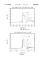
- FIG. 2 there is shown the change in the unidirectional anisotropy field (H UA ) or pinning field versus temperature for 5 nm thick Ni-Fe pinned layers using Fe-Mn, NiO and Ni-Mn as the pinning layers.
- Fe-Mn has a blocking temperature of about 180° C. (curve 210) and NiO has a blocking temperature of about 220° C. (curve 220).
- a typical SV sensor used in a magnetic recording disk drive should be able to operate reliably at a constant temperature of about 120° C. with a pinning field of at least 200 Oe, it can readily be seen that Fe-Mn substantially loses it ability to pin the pinned layer at about 120° C.
- Ni-Mn with a blocking temperature of beyond 450° C. (curve 230) easily meets the pinning field requirements at the 120° C. operating temperature of typical SV sensors.
- Ni-Mn AFM pinning layer is the requirement for high temperature (equal or greater than 240° C.) annealing step after the deposition of the SV sensor layers (post-annealing) to achieve the desired exchange coupling between the Ni-Mn pinning layer and the Ni-Fe pinned layer in order to achieve proper SV sensor operation.
- high temperature equal or greater than 240° C.
- annealing at such high temperature substantially degrades the GMR coefficient of the SV sensor.
- an SV sensor with the preferred structure of Ta/Ni-Mn/Ni-Fe/Co/Cu/Co/Ni-Fe/Ta where the Ni-Fe pinned layer is formed over the Ni-Mn antiferromagnetic layer and the combination of Ni-Mn and Ni-Fe layers is first annealed before depositing the rest of the SV layers.
- Carrying out the high temperature annealing process of the combination of Ni-Mn and Ni-Fe layers prior to deposition of the rest of the SV layers provides the exchange coupling field necessary to pin the Ni-Fe pinned layer without exposing the rest of the SV layers to the high temperature annealing process thus avoiding lowering the GMR effect.
- FIG. 1 is a schematic diagram of the cross-section of a prior art SV sensor
- FIG. 2 is a graph showing temperature dependence of the pinning fields for exchange coupling of Fe-Mn, NiO and Ni-Mn antiferromagnetic pinning layers to Ni-Fe ferromagnetic pinned layers;
- FIG. 3 is a perspective drawing of a magnetic recording disk drive system
- FIG. 4 is a schematic diagram of the cross-section of the preferred SV sensor of the present invention.
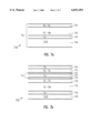
- FIGS. 5a and 5b are schematic diagrams of the cross-section of the thin film structure of the present invention at two stages of the deposition process
- FIGS. 6a and 6b are graphs showing the high field magnetoresistance hysteresis curves of SV sensors fabricated with post-anneal (prior art) and pre-anneal (applicant's invention) processes, respectively, of the Ni-Mn/Ni-Fe layers; and
- FIGS. 7a and 7b are schematic diagrams of the cross-sections of the thin film structure of an alternate embodiment of the present invention at two stages of the deposition process.
- FIG. 3 there is shown a disk drive 300 embodying the present invention.
- a disk drive 300 embodying the present invention.
- at least one rotatable magnetic disk 312 is supported on a spindle 314 and rotated by a disk drive motor 318.
- the magnetic recording media on each disk is in the form of an annular pattern of concentric data tracks (not shown) on disk 312.
- At least one slider 313 is positioned on the disk 312, each slider 313 supporting one or more magnetic read/write heads 321 where the head 321 incorporates the MR sensor of the present invention. As the disks rotate, slider 313 is moved radially in and out over disk surface 322 so that heads 321 may access different portions of the disk where desired data are recorded.
- Each slider 313 is attached to an actuator arm 319 by means of a suspension 315.
- the suspension 315 provides a slight spring force which biases slider 313 against the disk surface 322.
- Each actuator arm 319 is attached to an actuator means 327.
- the actuator means as shown in FIG. 3 may be a voice coil motor (VCM).
- VCM comprises a coil movable within a fixed magnetic field, the direction and speed of the coil movements being controlled by the motor current signals supplied by controller 329.
- the rotation of disk 312 generates an air bearing between slider 313 and disk surface 322 which exerts an upward force or lift on the slider.
- the air bearing thus counter-balances the slight spring force of suspension 315 and supports slider 313 off and slightly above the disk surface by a small, substantially constant spacing during normal operation.
- control unit 329 The various components of the disk storage system are controlled in operation by control signals generated by control unit 329, such as access control signals and internal clock signals.
- control unit 329 comprises logic control circuits, storage means and a microprocessor.
- the control unit 329 generates control signals to control various system operations such as drive motor control signals on line 323 and head position and seek control signals on line 328.
- the control signals on line 328 provide the desired current profiles to optimally move and position slider 313 to the desired data track on disk 312.
- Read and write signals are communicated to and from read/write heads 321 by means of recording channel 325.
- disk storage systems may contain a large number of disks and actuators, and each actuator may support a number of sliders.
- FIG. 4 there is shown an air bearing surface (ABS) view of the SV sensor 400 having the structure of Ta/Ni-Mn/Ni-Fe/Co/Cu/Co/Ni-Fe/Ta and manufactured, using a sputter deposition process, according to the preferred embodiment of the present invention.
- SV sensor 400 comprises end regions 404 and 406 separated by a central region 402.
- the magnetization of the pinned layer 420 is fixed by an antiferromagnetic (AFM) layer 425.
- An underlayer 429, AFM layer 425, pinned layer 420, spacer layer 415, free layer 410, and a cap layer 408 are all formed in that order in the central region 402.
- the underlayer 429 or seed layer is any layer deposited to modify the crystallographic texture or grain size of the subsequent layers, and may not be needed depending on the substrate. If used, the underlayer may be formed of tantalum (Ta), zirconium (Zr), hafnium (Hf), or yttrium (Y).
- the SV sensor 400 further comprises layers 430 and 435 formed in the end regions 404 and 406, respectively, for providing a longitudinal bias field to the free layer 410 to ensure a single magnetic domain state in the free layer.
- Layers 430 and 435 preferably made of hard magnetic material such as CoPtCr, are deposited and magnetically aligned at room temperature according to the well known methods established in the prior art.
- Lead layers 440 and 445 are formed over hard bias layers 430 and 435 in the end regions 404 and 406, respectively, by the methods known to the prior art.
- Leads 440 and 445 provide electrical connections for the flow of the sensing current I s from a current source 460 to the SV sensor 400.
- Sensing means 470 connected to leads 440 and 445 sense the change in the resistance due to changes induced in the free layer 410 by the external magnetic field (e.g., field generated by a data bit stored on a disk).
- the sputter deposition process for fabrication of the SV sensor 400 is started with deposition on a substrate 528 of a suitable underlayer material such as Ta 526 followed by deposition of a Ni-Mn antiferromagnetic (AFM) pinning layer 525.
- the preferred composition of the Ni-Mn AFM layer is a Mn composition in the range between 46 and 60 percent.
- a Ni-Fe pinned layer 521 is subsequently deposited in direct contact and overlaying the Ni-Mn pinning layer 525 followed by a Ta layer 523 to protectively cap the deposited layers.
- annealing of the deposited layers 532 is carried out to increase exchange coupling between the Ni-Mn pinning layer 525 and the Ni-Fe pinned layer 521.
- the annealing temperature required to increase exchange coupling is equal to or greater than 240° C.
- this anneal step may be carried out ex-situ (that is, outside the sputter deposition system) in an external vacuum oven.
- Annealing may be carried out at temperatures ranging from 240° C. to 320° C. At the lower annealing temperatures a longer anneal time is required than at higher temperatures to achieve sufficient exchange coupling in the Ni-Mn/Ni-Fe layers.
- Annealing in a high vacuum oven at 320° C. for a time period in the range from 20 minutes to 100 hours results in sufficient exchange coupling between the AWM and pinned layers.
- annealing may be carried out at 240° C. for a time period in the range of 2 hours to 100 hours.
- the annealing step is carried out at 255° C. for 10 hours with the deposited layers 532 in a transverse magnetic field 580 (perpendicular to the air bearing surface).
- ion milling or reactive ion etching (RIE) is used to remove the Ta cap layer 523 and part of the Ni-Fe pinned layer 521.
- the Ni-Fe pinned layer 521 is removed at this step to ensure having a clean Ni-Fe exposed surface.
- the Ni-Fe pinned layer 521 must not be removed totally to ensure maintenance of exchange coupling between the Ni-Mn and Ni-Fe layers.
- the film structure 530 is then returned to the sputter deposition system for further processing according to the present invention.
- the remainder of the SV structure is sputter deposited on the exposed Ni-Fe pinned layer 521 in the presence of a longitudinal magnetic field 585 (parallel to the air bearing surface).
- Thin Co layer 522 is deposited over and in contact with the Ni-Fe pinned layer 521, followed by a thin Cu spacer layer 515, another thin Co layer 512, a Ni-Fe free layer 511 and a Ta cap layer 505.
- the pinned layer 520 comprises a Ni-Fe pinned layer 521 and a thin Co layer 522.
- the free layer 510 comprises a thin Co layer 512 and a Ni-Fe free layer 511. This completes processing of the central region of the SV structure of the preferred embodiment of the present invention.
- end regions are formed which include depositing horizontal bias layers and leads according to the well known methods established in the prior art.
- FIG. 6a is a graph of the high field magnetoresistance hysteresis curves obtained at room temperature (RT) 610 and at 120° C. 620 for a prior art Ta/Ni-Fe/Co/Cu/Co/Ni-Fe/Ni-Mn/Ta SV sensor annealed after deposition of the entire layer structure (post-annealed).
- FIG. 6b is a graph of the high field magnetoresistance hysteresis curves obtained at RT 630 and at 120° C.
- Ta/Ni-Mn/Ni-Fe/Co/Cu/Co/Ni-Fe/Ta SV sensor processed according to the present invention by pre-annealing the combination of the Ni-Mn AFM and Ni-Fe pinned layers prior to depositing the remaining SV sensor layers in order to avoid degradation of the SV sensor performance.
- Table I shows the giant magnetoresistive (GMR) coefficients (deltaR/R) for the prior art and present invention SV devices taken from FIGS. 6a and 6b.
- GMR giant magnetoresistive
- a sputter deposition system capable of deposition of the free and pinned ferromagnetic layers in longitudinal and transverse magnetic fields, respectively, and having capability for in-situ (that is, in place in the sputter deposition system) annealing is used.
- the Ta/Ni-Mn/Ni-Fe/Co/Cu/Co/Ni-Fe/Ta SV sensor structure is fabricated by first depositing the Ta 726, Ni-Mn 725 and Ni-Fe 720 layers on the substrate 728. The structure is then annealed in-situ at a temperature in the range of 240° C. to 320° C. in the presence of a transverse magnetic field. At a temperature of 320° C., an in-situ anneal time of 20 minutes is sufficient to achieve the desired exchange coupling between the Ni-Mn and Ni-Fe layers.
- annealing times ranging from 20 minutes up 100 hours can also be used to obtain large exchange coupling without degradation of the SV effect due to interdiffusion at the layer interfaces.
- an in situ time of about 10 hours is sufficient to achieve the desired exchange coupling between the AFM and pinned layers.
- This process of in-situ annealing simplifies the processing by eliminating the intermediate Ta capping process and the subsequent ion-milling to remove the intermediate Ta cap layer and a portion of the pinned layer required in the preferred embodiment described above.
- the fabrication methods of the preferred embodiment and the alternative embodiment described herein may be used to fabricate SV sensors having the layered structure Ta/Ni-Mn/Ni-Fe/Cu/Ni-Fe/Ta or SV sensors having the layered structure Ta/Ni-Mn/Ni-Fe/Co/Cu/Ni-Fe/Ta or SV sensors having the layered structure Ni-Mn/pinned layer/spacer/free layer.
- AFM materials such as Pd-Mn and Pt-Mn with Mn composition in the 46-60% range may also be used to fabricate SV sensors according to the present invention.
- spacer layer materials such as gold and silver may also be used to fabricate SV sensors according to the present invention.
Abstract
Description
Claims (14)
Priority Applications (2)
| Application Number | Priority Date | Filing Date | Title |
|---|---|---|---|
| US08/922,963 US6033491A (en) | 1997-09-03 | 1997-09-03 | Fabrication process of Ni-Mn spin valve sensor |
| US08/949,065 US5993566A (en) | 1997-09-03 | 1997-10-10 | Fabrication process of Ni-Mn spin valve sensor |
Applications Claiming Priority (1)
| Application Number | Priority Date | Filing Date | Title |
|---|---|---|---|
| US08/922,963 US6033491A (en) | 1997-09-03 | 1997-09-03 | Fabrication process of Ni-Mn spin valve sensor |
Related Child Applications (1)
| Application Number | Title | Priority Date | Filing Date |
|---|---|---|---|
| US08/949,065 Continuation-In-Part US5993566A (en) | 1997-09-03 | 1997-10-10 | Fabrication process of Ni-Mn spin valve sensor |
Publications (1)
| Publication Number | Publication Date |
|---|---|
| US6033491A true US6033491A (en) | 2000-03-07 |
Family
ID=25447881
Family Applications (1)
| Application Number | Title | Priority Date | Filing Date |
|---|---|---|---|
| US08/922,963 Expired - Fee Related US6033491A (en) | 1997-09-03 | 1997-09-03 | Fabrication process of Ni-Mn spin valve sensor |
Country Status (1)
| Country | Link |
|---|---|
| US (1) | US6033491A (en) |
Cited By (29)
| Publication number | Priority date | Publication date | Assignee | Title |
|---|---|---|---|---|
| US6181535B1 (en) * | 1998-03-06 | 2001-01-30 | Tdk Corporation | Magnetoresistance effect head obtained using a pulse magnetic field process |
| US6364964B1 (en) * | 1999-09-06 | 2002-04-02 | Tdk Corporation | Manufacturing method of spin valve magnetoresistive effect element and manufacturing method of thin-film magnetic head with the element |
| US6364961B1 (en) * | 1997-09-11 | 2002-04-02 | Fujitsu Limited | Spin-valve magnetic head with the pinned layer having different directions for its magnetization axis and its easy axis |
| US20030096057A1 (en) * | 2000-08-07 | 2003-05-22 | Headway Technologies, Inc. | Spin filter bottom spin valve head with continuous spacer exchange bias |
| US20030113582A1 (en) * | 2001-11-29 | 2003-06-19 | Seagate Technology Llc | Selective annealing of magnetic recording films |
| US20030137780A1 (en) * | 2002-01-18 | 2003-07-24 | International Business Machines Corporation | High linear density tunnel junction flux guide read head with in-stack longitudinal bias stack (LBS) |
| US6657825B2 (en) | 2001-08-02 | 2003-12-02 | International Business Machines Corporation | Self aligned magnetoresistive flux guide read head with exchange bias underneath free layer |
| US6700757B2 (en) | 2001-01-02 | 2004-03-02 | Hitachi Global Storage Technologies Netherlands B.V. | Enhanced free layer for a spin valve sensor |
| US6728083B2 (en) | 2001-06-26 | 2004-04-27 | Hitachi Global Storage Technologies Netherlands B.V. | Method of making a spin valve sensor with a controlled ferromagnetic coupling field |
| US6744607B2 (en) | 2002-03-21 | 2004-06-01 | Hitachi Global Storage Technologies Netherlands B.V. | Exchange biased self-pinned spin valve sensor with recessed overlaid leads |
| US6754056B2 (en) | 2002-01-18 | 2004-06-22 | International Business Machines Corporation | Read head having a tunnel junction sensor with a free layer biased by exchange coupling with insulating antiferromagnetic (AFM) layers |
| US6757144B2 (en) | 2002-01-18 | 2004-06-29 | International Business Machines Corporation | Flux guide read head with in stack biased current perpendicular to the planes (CPP) sensor |
| US20050141146A1 (en) * | 2001-06-26 | 2005-06-30 | Pinarbasi Mustafa M. | Method of making a tunnel valve sensor with improved free layer sensitivity |
| US6998061B1 (en) * | 2002-09-06 | 2006-02-14 | Maxtor Corporation | In-situ exchange biased GMR head for ultra-high density recording with pinning layer-only anneal |
| US7166320B1 (en) * | 2000-02-14 | 2007-01-23 | Seagate Technology Llc | Post-deposition annealed recording media and method of manufacturing the same |
| US20070064353A1 (en) * | 2005-09-20 | 2007-03-22 | Heim David E | Read sensor defined by lateral stack templates and method for fabrication |
| US20110102949A1 (en) * | 2009-11-03 | 2011-05-05 | Western Digital (Fremont), Llc | Method to improve reader stability and writer overwrite by patterned wafer annealing |
| US8760819B1 (en) | 2010-12-23 | 2014-06-24 | Western Digital (Fremont), Llc | Magnetic recording sensor with sputtered antiferromagnetic coupling trilayer between plated ferromagnetic shields |
| US8780505B1 (en) | 2013-03-12 | 2014-07-15 | Western Digital (Fremont), Llc | Method and system for providing a read transducer having an improved composite magnetic shield |
| US8797692B1 (en) | 2012-09-07 | 2014-08-05 | Western Digital (Fremont), Llc | Magnetic recording sensor with AFM exchange coupled shield stabilization |
| US8883017B1 (en) * | 2013-03-12 | 2014-11-11 | Western Digital (Fremont), Llc | Method and system for providing a read transducer having seamless interfaces |
| US9013836B1 (en) | 2013-04-02 | 2015-04-21 | Western Digital (Fremont), Llc | Method and system for providing an antiferromagnetically coupled return pole |
| US9064534B1 (en) | 2012-11-30 | 2015-06-23 | Western Digital (Fremont), Llc | Process for providing a magnetic recording transducer with enhanced pinning layer stability |
| US9147408B1 (en) | 2013-12-19 | 2015-09-29 | Western Digital (Fremont), Llc | Heated AFM layer deposition and cooling process for TMR magnetic recording sensor with high pinning field |
| US9287494B1 (en) | 2013-06-28 | 2016-03-15 | Western Digital (Fremont), Llc | Magnetic tunnel junction (MTJ) with a magnesium oxide tunnel barrier |
| US9361913B1 (en) | 2013-06-03 | 2016-06-07 | Western Digital (Fremont), Llc | Recording read heads with a multi-layer AFM layer methods and apparatuses |
| US9431047B1 (en) | 2013-05-01 | 2016-08-30 | Western Digital (Fremont), Llc | Method for providing an improved AFM reader shield |
| US10074387B1 (en) | 2014-12-21 | 2018-09-11 | Western Digital (Fremont), Llc | Method and system for providing a read transducer having symmetric antiferromagnetically coupled shields |
| US11204263B2 (en) * | 2017-10-31 | 2021-12-21 | Tdk Corporation | Position detection device for detecting position of an object moving in a predetermined direction, and a magnetic sensor for use with the position detection device |
Citations (7)
| Publication number | Priority date | Publication date | Assignee | Title |
|---|---|---|---|---|
| US5014147A (en) * | 1989-10-31 | 1991-05-07 | International Business Machines Corporation | Magnetoresistive sensor with improved antiferromagnetic film |
| US5206590A (en) * | 1990-12-11 | 1993-04-27 | International Business Machines Corporation | Magnetoresistive sensor based on the spin valve effect |
| US5315468A (en) * | 1992-07-28 | 1994-05-24 | International Business Machines Corporation | Magnetoresistive sensor having antiferromagnetic layer for exchange bias |
| US5373238A (en) * | 1992-11-06 | 1994-12-13 | International Business Machines Corporation | Four layer magnetoresistance device and method for making a four layer magnetoresistance device |
| US5492720A (en) * | 1994-08-15 | 1996-02-20 | International Business Machines Corporation | Method of manufacturing a magnetoresistive sensor |
| US5561368A (en) * | 1994-11-04 | 1996-10-01 | International Business Machines Corporation | Bridge circuit magnetic field sensor having spin valve magnetoresistive elements formed on common substrate |
| US5772794A (en) * | 1995-10-09 | 1998-06-30 | Tdk Corporation | Manufacturing method of magnetic head apparatus with spin valve effect magnetoresistive head |
-
1997
- 1997-09-03 US US08/922,963 patent/US6033491A/en not_active Expired - Fee Related
Patent Citations (8)
| Publication number | Priority date | Publication date | Assignee | Title |
|---|---|---|---|---|
| US5014147A (en) * | 1989-10-31 | 1991-05-07 | International Business Machines Corporation | Magnetoresistive sensor with improved antiferromagnetic film |
| US5206590A (en) * | 1990-12-11 | 1993-04-27 | International Business Machines Corporation | Magnetoresistive sensor based on the spin valve effect |
| US5315468A (en) * | 1992-07-28 | 1994-05-24 | International Business Machines Corporation | Magnetoresistive sensor having antiferromagnetic layer for exchange bias |
| US5436778A (en) * | 1992-07-28 | 1995-07-25 | International Business Machines Corporation | Magnetoresistive sensor having antiferromagnetic exchange bias |
| US5373238A (en) * | 1992-11-06 | 1994-12-13 | International Business Machines Corporation | Four layer magnetoresistance device and method for making a four layer magnetoresistance device |
| US5492720A (en) * | 1994-08-15 | 1996-02-20 | International Business Machines Corporation | Method of manufacturing a magnetoresistive sensor |
| US5561368A (en) * | 1994-11-04 | 1996-10-01 | International Business Machines Corporation | Bridge circuit magnetic field sensor having spin valve magnetoresistive elements formed on common substrate |
| US5772794A (en) * | 1995-10-09 | 1998-06-30 | Tdk Corporation | Manufacturing method of magnetic head apparatus with spin valve effect magnetoresistive head |
Non-Patent Citations (6)
| Title |
|---|
| "Exchange-Coupled Ni--Fe/Fe--Mn, Ni--Mn and NiO/Ni--Fe Films for Stabilization of Magnetoresistive Sensors", T. Lin, et al., IEEE Trans. on Mags., vol. 31, No. 6, Nov. 1995, pp. 2585-2590. |
| "Improved Exchange Coupling Between Ferrogmagnetic Ni--Fe and Antiferrogmagnetic Ni--Mn--Based Films", T. Lin et al., App.Phys.Lett 65 (9), Aug. 29, 1994, pp. 1183-1185. |
| "NiMn--Pinned Spin Valves With Pinning Field Made by Ion Beam Sputtering", S. Mao et al., Appl.Phys.Lett. 69 (23), Dec. 2, 1996, pp. 3593-3595. |
| Exchange Coupled Ni Fe/Fe Mn, Ni Mn and NiO/Ni Fe Films for Stabilization of Magnetoresistive Sensors , T. Lin, et al., IEEE Trans. on Mags., vol. 31, No. 6, Nov. 1995, pp. 2585 2590. * |
| Improved Exchange Coupling Between Ferrogmagnetic Ni Fe and Antiferrogmagnetic Ni Mn Based Films , T. Lin et al., App.Phys.Lett 65 (9), Aug. 29, 1994, pp. 1183 1185. * |
| NiMn Pinned Spin Valves With Pinning Field Made by Ion Beam Sputtering , S. Mao et al., Appl.Phys.Lett. 69 (23), Dec. 2, 1996, pp. 3593 3595. * |
Cited By (41)
| Publication number | Priority date | Publication date | Assignee | Title |
|---|---|---|---|---|
| US6364961B1 (en) * | 1997-09-11 | 2002-04-02 | Fujitsu Limited | Spin-valve magnetic head with the pinned layer having different directions for its magnetization axis and its easy axis |
| US6181535B1 (en) * | 1998-03-06 | 2001-01-30 | Tdk Corporation | Magnetoresistance effect head obtained using a pulse magnetic field process |
| US6364964B1 (en) * | 1999-09-06 | 2002-04-02 | Tdk Corporation | Manufacturing method of spin valve magnetoresistive effect element and manufacturing method of thin-film magnetic head with the element |
| US7166320B1 (en) * | 2000-02-14 | 2007-01-23 | Seagate Technology Llc | Post-deposition annealed recording media and method of manufacturing the same |
| US20030096057A1 (en) * | 2000-08-07 | 2003-05-22 | Headway Technologies, Inc. | Spin filter bottom spin valve head with continuous spacer exchange bias |
| US6962663B2 (en) * | 2000-08-07 | 2005-11-08 | Headway Technologies, Inc. | Process for manufacturing a read head |
| US6700757B2 (en) | 2001-01-02 | 2004-03-02 | Hitachi Global Storage Technologies Netherlands B.V. | Enhanced free layer for a spin valve sensor |
| US7088561B2 (en) * | 2001-06-26 | 2006-08-08 | Hitachi Gloabl Storage Technolgies Netherlands B.V. | Method of making a tunnel valve sensor with improved free layer sensitivity |
| US20040169964A1 (en) * | 2001-06-26 | 2004-09-02 | Hitachi Global Storage Technologies Netherlands B.V, | Method of making a spin valve sensor with a controlled ferromagnetic coupling field |
| US20050141146A1 (en) * | 2001-06-26 | 2005-06-30 | Pinarbasi Mustafa M. | Method of making a tunnel valve sensor with improved free layer sensitivity |
| US6728083B2 (en) | 2001-06-26 | 2004-04-27 | Hitachi Global Storage Technologies Netherlands B.V. | Method of making a spin valve sensor with a controlled ferromagnetic coupling field |
| US20040061979A1 (en) * | 2001-08-02 | 2004-04-01 | Ho Kuok San | Self aligned magnetoresistive flux guide read head with exchange bias underneath free layer |
| US7036208B2 (en) | 2001-08-02 | 2006-05-02 | Hitachi Global Storagetechnologies Netherlands B.V | Self aligned magnetoresistive flux guide read head with exchange bias underneath free layer |
| US6657825B2 (en) | 2001-08-02 | 2003-12-02 | International Business Machines Corporation | Self aligned magnetoresistive flux guide read head with exchange bias underneath free layer |
| US20030113582A1 (en) * | 2001-11-29 | 2003-06-19 | Seagate Technology Llc | Selective annealing of magnetic recording films |
| US6884328B2 (en) * | 2001-11-29 | 2005-04-26 | Seagate Technology Llc | Selective annealing of magnetic recording films |
| US6757144B2 (en) | 2002-01-18 | 2004-06-29 | International Business Machines Corporation | Flux guide read head with in stack biased current perpendicular to the planes (CPP) sensor |
| US6888705B2 (en) | 2002-01-18 | 2005-05-03 | Hitachi Global Storage Technologies Netherlands B.V. | High linear density tunnel junction flux guide read head with in-stack longitudinal bias stack (LBS) |
| US20050146812A1 (en) * | 2002-01-18 | 2005-07-07 | Hitachi Global Storage Technologies Netherlands B.V. | High linear density tunnel junction flux guide read head with in-stack longitudinal bias stack (LBS) |
| US20040196596A1 (en) * | 2002-01-18 | 2004-10-07 | Ho Kuok San | Method of making a read head having a tunnel junction sensor with a free layer biased by exchange coupling with insulating antiferromagnetic (AFM) layers |
| US6754056B2 (en) | 2002-01-18 | 2004-06-22 | International Business Machines Corporation | Read head having a tunnel junction sensor with a free layer biased by exchange coupling with insulating antiferromagnetic (AFM) layers |
| US20030137780A1 (en) * | 2002-01-18 | 2003-07-24 | International Business Machines Corporation | High linear density tunnel junction flux guide read head with in-stack longitudinal bias stack (LBS) |
| US7161773B2 (en) | 2002-01-18 | 2007-01-09 | Hitachi Global Storage Technologies Netherlands B.V. | High linear density tunnel junction flux guide read head with in-stack longitudinal bias stack (LBS) |
| US6744607B2 (en) | 2002-03-21 | 2004-06-01 | Hitachi Global Storage Technologies Netherlands B.V. | Exchange biased self-pinned spin valve sensor with recessed overlaid leads |
| US6998061B1 (en) * | 2002-09-06 | 2006-02-14 | Maxtor Corporation | In-situ exchange biased GMR head for ultra-high density recording with pinning layer-only anneal |
| US7472469B2 (en) * | 2005-09-20 | 2009-01-06 | Hitachi Global Storage Technologies Netherlands B.V. | Method for fabricating a magnetic head having a sensor stack and two lateral stack |
| US20070064353A1 (en) * | 2005-09-20 | 2007-03-22 | Heim David E | Read sensor defined by lateral stack templates and method for fabrication |
| US20110102949A1 (en) * | 2009-11-03 | 2011-05-05 | Western Digital (Fremont), Llc | Method to improve reader stability and writer overwrite by patterned wafer annealing |
| US8336194B2 (en) | 2009-11-03 | 2012-12-25 | Western Digital (Fremont), Llc | Method of fabricating a tunneling magnetoresistive (TMR) reader |
| US8760819B1 (en) | 2010-12-23 | 2014-06-24 | Western Digital (Fremont), Llc | Magnetic recording sensor with sputtered antiferromagnetic coupling trilayer between plated ferromagnetic shields |
| US8797692B1 (en) | 2012-09-07 | 2014-08-05 | Western Digital (Fremont), Llc | Magnetic recording sensor with AFM exchange coupled shield stabilization |
| US9064534B1 (en) | 2012-11-30 | 2015-06-23 | Western Digital (Fremont), Llc | Process for providing a magnetic recording transducer with enhanced pinning layer stability |
| US8780505B1 (en) | 2013-03-12 | 2014-07-15 | Western Digital (Fremont), Llc | Method and system for providing a read transducer having an improved composite magnetic shield |
| US8883017B1 (en) * | 2013-03-12 | 2014-11-11 | Western Digital (Fremont), Llc | Method and system for providing a read transducer having seamless interfaces |
| US9013836B1 (en) | 2013-04-02 | 2015-04-21 | Western Digital (Fremont), Llc | Method and system for providing an antiferromagnetically coupled return pole |
| US9431047B1 (en) | 2013-05-01 | 2016-08-30 | Western Digital (Fremont), Llc | Method for providing an improved AFM reader shield |
| US9361913B1 (en) | 2013-06-03 | 2016-06-07 | Western Digital (Fremont), Llc | Recording read heads with a multi-layer AFM layer methods and apparatuses |
| US9287494B1 (en) | 2013-06-28 | 2016-03-15 | Western Digital (Fremont), Llc | Magnetic tunnel junction (MTJ) with a magnesium oxide tunnel barrier |
| US9147408B1 (en) | 2013-12-19 | 2015-09-29 | Western Digital (Fremont), Llc | Heated AFM layer deposition and cooling process for TMR magnetic recording sensor with high pinning field |
| US10074387B1 (en) | 2014-12-21 | 2018-09-11 | Western Digital (Fremont), Llc | Method and system for providing a read transducer having symmetric antiferromagnetically coupled shields |
| US11204263B2 (en) * | 2017-10-31 | 2021-12-21 | Tdk Corporation | Position detection device for detecting position of an object moving in a predetermined direction, and a magnetic sensor for use with the position detection device |
Similar Documents
| Publication | Publication Date | Title |
|---|---|---|
| US6033491A (en) | Fabrication process of Ni-Mn spin valve sensor | |
| US6141191A (en) | Spin valves with enhanced GMR and thermal stability | |
| US6038107A (en) | Antiparallel-pinned spin valve sensor | |
| EP0585009B1 (en) | Magnetoresistive sensor | |
| US6127053A (en) | Spin valves with high uniaxial anisotropy reference and keeper layers | |
| US6040961A (en) | Current-pinned, current resettable soft AP-pinned spin valve sensor | |
| US5528440A (en) | Spin valve magnetoresistive element with longitudinal exchange biasing of end regions abutting the free layer, and magnetic recording system using the element | |
| US5408377A (en) | Magnetoresistive sensor with improved ferromagnetic sensing layer and magnetic recording system using the sensor | |
| US6780524B2 (en) | In-situ oxidized films for use as gap layers for a spin-valve sensor and methods of manufacture | |
| US5465185A (en) | Magnetoresistive spin valve sensor with improved pinned ferromagnetic layer and magnetic recording system using the sensor | |
| US5920446A (en) | Ultra high density GMR sensor | |
| US6117569A (en) | Spin valves with antiferromagnetic exchange pinning and high uniaxial anisotropy reference and keeper layers | |
| US5883764A (en) | Magnetoresistive sensor having multi-layered refractory metal conductor leads | |
| US6127045A (en) | Magnetic tunnel junction device with optimized ferromagnetic layer | |
| US5701223A (en) | Spin valve magnetoresistive sensor with antiparallel pinned layer and improved exchange bias layer, and magnetic recording system using the sensor | |
| US5583725A (en) | Spin valve magnetoresistive sensor with self-pinned laminated layer and magnetic recording system using the sensor | |
| US5583727A (en) | Multiple data layer magnetic recording data storage system with digital magnetoresistive read sensor | |
| US6636400B2 (en) | Magnetoresistive head having improved hard biasing characteristics through the use of a multi-layered seed layer including an oxidized tantalum layer and a chromium layer | |
| US5993566A (en) | Fabrication process of Ni-Mn spin valve sensor | |
| US6680828B2 (en) | Differential GMR head system and method using self-pinned layer | |
| KR100332992B1 (en) | Spin valve head with diffusion barrier | |
| US6175477B1 (en) | Spin valve sensor with nonmagnetic oxide seed layer | |
| US6175475B1 (en) | Fully-pinned, flux-closed spin valve | |
| US6178073B1 (en) | Magneto-resistance effect element with a fixing layer formed from a superlattice of at least two different materials and production method of the same | |
| US7428129B2 (en) | Methods and apparatus for improved hard magnet properties in magnetoresistive read heads using a multi-layered seed layer structure |
Legal Events
| Date | Code | Title | Description |
|---|---|---|---|
| AS | Assignment |
Owner name: INTERNATIONAL BUSINESS MACHINES CORPORATION, NEW Y Free format text: ASSIGNMENT OF ASSIGNORS INTEREST;ASSIGNOR:LIN, TSANN;REEL/FRAME:008699/0705 Effective date: 19970903 |
|
| FEPP | Fee payment procedure |
Free format text: PAYOR NUMBER ASSIGNED (ORIGINAL EVENT CODE: ASPN); ENTITY STATUS OF PATENT OWNER: LARGE ENTITY |
|
| AS | Assignment |
Owner name: MARIANA HDD B.V., NETHERLANDS Free format text: ASSIGNMENT OF ASSIGNORS INTEREST;ASSIGNOR:INTERNATIONAL BUSINESS MACHINES CORPORATION;REEL/FRAME:013663/0348 Effective date: 20021231 |
|
| AS | Assignment |
Owner name: HITACHI GLOBAL STORAGE TECHNOLOGIES NETHERLANDS B. Free format text: CHANGE OF NAME;ASSIGNOR:MARIANA HDD B.V.;REEL/FRAME:013746/0146 Effective date: 20021231 |
|
| FPAY | Fee payment |
Year of fee payment: 4 |
|
| FEPP | Fee payment procedure |
Free format text: PAYOR NUMBER ASSIGNED (ORIGINAL EVENT CODE: ASPN); ENTITY STATUS OF PATENT OWNER: LARGE ENTITY Free format text: PAYER NUMBER DE-ASSIGNED (ORIGINAL EVENT CODE: RMPN); ENTITY STATUS OF PATENT OWNER: LARGE ENTITY |
|
| FPAY | Fee payment |
Year of fee payment: 8 |
|
| REMI | Maintenance fee reminder mailed | ||
| LAPS | Lapse for failure to pay maintenance fees | ||
| STCH | Information on status: patent discontinuation |
Free format text: PATENT EXPIRED DUE TO NONPAYMENT OF MAINTENANCE FEES UNDER 37 CFR 1.362 |
|
| FP | Lapsed due to failure to pay maintenance fee |
Effective date: 20120307 |