US6064157A - Flat panel display with common bus structure - Google Patents
Flat panel display with common bus structure Download PDFInfo
- Publication number
- US6064157A US6064157A US09/161,165 US16116598A US6064157A US 6064157 A US6064157 A US 6064157A US 16116598 A US16116598 A US 16116598A US 6064157 A US6064157 A US 6064157A
- Authority
- US
- United States
- Prior art keywords
- spacer
- flat panel
- faceplate
- panel display
- backplate
- Prior art date
- Legal status (The legal status is an assumption and is not a legal conclusion. Google has not performed a legal analysis and makes no representation as to the accuracy of the status listed.)
- Expired - Lifetime
Links
- 125000006850 spacer group Chemical group 0.000 claims abstract description 207
- 239000003990 capacitor Substances 0.000 claims description 31
- 239000000463 material Substances 0.000 description 18
- GWEVSGVZZGPLCZ-UHFFFAOYSA-N Titan oxide Chemical compound O=[Ti]=O GWEVSGVZZGPLCZ-UHFFFAOYSA-N 0.000 description 11
- 230000004913 activation Effects 0.000 description 10
- OGIDPMRJRNCKJF-UHFFFAOYSA-N titanium oxide Inorganic materials [Ti]=O OGIDPMRJRNCKJF-UHFFFAOYSA-N 0.000 description 10
- 235000012431 wafers Nutrition 0.000 description 9
- WGLPBDUCMAPZCE-UHFFFAOYSA-N Trioxochromium Chemical compound O=[Cr](=O)=O WGLPBDUCMAPZCE-UHFFFAOYSA-N 0.000 description 8
- 239000000919 ceramic Substances 0.000 description 8
- 229910000423 chromium oxide Inorganic materials 0.000 description 8
- 239000011159 matrix material Substances 0.000 description 7
- 239000004020 conductor Substances 0.000 description 6
- TWNQGVIAIRXVLR-UHFFFAOYSA-N oxo(oxoalumanyloxy)alumane Chemical compound O=[Al]O[Al]=O TWNQGVIAIRXVLR-UHFFFAOYSA-N 0.000 description 6
- 238000010304 firing Methods 0.000 description 4
- 239000000843 powder Substances 0.000 description 4
- 239000004065 semiconductor Substances 0.000 description 4
- YXFVVABEGXRONW-UHFFFAOYSA-N Toluene Chemical compound CC1=CC=CC=C1 YXFVVABEGXRONW-UHFFFAOYSA-N 0.000 description 3
- 230000003213 activating effect Effects 0.000 description 3
- 238000010586 diagram Methods 0.000 description 3
- 239000011521 glass Substances 0.000 description 3
- 239000000203 mixture Substances 0.000 description 3
- 239000002002 slurry Substances 0.000 description 3
- LFQSCWFLJHTTHZ-UHFFFAOYSA-N Ethanol Chemical compound CCO LFQSCWFLJHTTHZ-UHFFFAOYSA-N 0.000 description 2
- UFHFLCQGNIYNRP-UHFFFAOYSA-N Hydrogen Chemical compound [H][H] UFHFLCQGNIYNRP-UHFFFAOYSA-N 0.000 description 2
- OAICVXFJPJFONN-UHFFFAOYSA-N Phosphorus Chemical compound [P] OAICVXFJPJFONN-UHFFFAOYSA-N 0.000 description 2
- 239000004642 Polyimide Substances 0.000 description 2
- VYPSYNLAJGMNEJ-UHFFFAOYSA-N Silicium dioxide Chemical compound O=[Si]=O VYPSYNLAJGMNEJ-UHFFFAOYSA-N 0.000 description 2
- 229910052770 Uranium Inorganic materials 0.000 description 2
- 238000000576 coating method Methods 0.000 description 2
- 150000001875 compounds Chemical class 0.000 description 2
- 238000001803 electron scattering Methods 0.000 description 2
- 239000001257 hydrogen Substances 0.000 description 2
- 229910052739 hydrogen Inorganic materials 0.000 description 2
- 238000000034 method Methods 0.000 description 2
- 239000003607 modifier Substances 0.000 description 2
- 239000011295 pitch Substances 0.000 description 2
- 229920001721 polyimide Polymers 0.000 description 2
- 230000004044 response Effects 0.000 description 2
- 238000005245 sintering Methods 0.000 description 2
- 239000007787 solid Substances 0.000 description 2
- 229910000314 transition metal oxide Inorganic materials 0.000 description 2
- 229910018404 Al2 O3 Inorganic materials 0.000 description 1
- RYGMFSIKBFXOCR-UHFFFAOYSA-N Copper Chemical compound [Cu] RYGMFSIKBFXOCR-UHFFFAOYSA-N 0.000 description 1
- 230000009471 action Effects 0.000 description 1
- 229910052782 aluminium Inorganic materials 0.000 description 1
- XAGFODPZIPBFFR-UHFFFAOYSA-N aluminium Chemical compound [Al] XAGFODPZIPBFFR-UHFFFAOYSA-N 0.000 description 1
- QVGXLLKOCUKJST-UHFFFAOYSA-N atomic oxygen Chemical compound [O] QVGXLLKOCUKJST-UHFFFAOYSA-N 0.000 description 1
- 239000011230 binding agent Substances 0.000 description 1
- BRPQOXSCLDDYGP-UHFFFAOYSA-N calcium oxide Chemical compound [O-2].[Ca+2] BRPQOXSCLDDYGP-UHFFFAOYSA-N 0.000 description 1
- 239000000292 calcium oxide Substances 0.000 description 1
- ODINCKMPIJJUCX-UHFFFAOYSA-N calcium oxide Inorganic materials [Ca]=O ODINCKMPIJJUCX-UHFFFAOYSA-N 0.000 description 1
- 239000011195 cermet Substances 0.000 description 1
- 239000002131 composite material Substances 0.000 description 1
- 238000007796 conventional method Methods 0.000 description 1
- 229910052802 copper Inorganic materials 0.000 description 1
- 239000010949 copper Substances 0.000 description 1
- QDOXWKRWXJOMAK-UHFFFAOYSA-N dichromium trioxide Chemical compound O=[Cr]O[Cr]=O QDOXWKRWXJOMAK-UHFFFAOYSA-N 0.000 description 1
- 230000005684 electric field Effects 0.000 description 1
- 230000005496 eutectics Effects 0.000 description 1
- 239000003574 free electron Substances 0.000 description 1
- 239000011810 insulating material Substances 0.000 description 1
- 239000012212 insulator Substances 0.000 description 1
- 239000000395 magnesium oxide Substances 0.000 description 1
- CPLXHLVBOLITMK-UHFFFAOYSA-N magnesium oxide Inorganic materials [Mg]=O CPLXHLVBOLITMK-UHFFFAOYSA-N 0.000 description 1
- AXZKOIWUVFPNLO-UHFFFAOYSA-N magnesium;oxygen(2-) Chemical compound [O-2].[Mg+2] AXZKOIWUVFPNLO-UHFFFAOYSA-N 0.000 description 1
- 238000004519 manufacturing process Methods 0.000 description 1
- 229910052751 metal Inorganic materials 0.000 description 1
- 239000002184 metal Substances 0.000 description 1
- 239000002923 metal particle Substances 0.000 description 1
- 150000002739 metals Chemical class 0.000 description 1
- 238000012986 modification Methods 0.000 description 1
- 230000004048 modification Effects 0.000 description 1
- 239000003921 oil Substances 0.000 description 1
- 239000001301 oxygen Substances 0.000 description 1
- 229910052760 oxygen Inorganic materials 0.000 description 1
- 230000000737 periodic effect Effects 0.000 description 1
- 229920002037 poly(vinyl butyral) polymer Polymers 0.000 description 1
- 238000000197 pyrolysis Methods 0.000 description 1
- 239000002994 raw material Substances 0.000 description 1
- 239000000377 silicon dioxide Substances 0.000 description 1
- 235000012239 silicon dioxide Nutrition 0.000 description 1
- 239000002904 solvent Substances 0.000 description 1
- 238000000638 solvent extraction Methods 0.000 description 1
Images


Classifications
-
- H—ELECTRICITY
- H01—ELECTRIC ELEMENTS
- H01J—ELECTRIC DISCHARGE TUBES OR DISCHARGE LAMPS
- H01J31/00—Cathode ray tubes; Electron beam tubes
- H01J31/08—Cathode ray tubes; Electron beam tubes having a screen on or from which an image or pattern is formed, picked up, converted, or stored
- H01J31/10—Image or pattern display tubes, i.e. having electrical input and optical output; Flying-spot tubes for scanning purposes
- H01J31/12—Image or pattern display tubes, i.e. having electrical input and optical output; Flying-spot tubes for scanning purposes with luminescent screen
- H01J31/123—Flat display tubes
-
- H—ELECTRICITY
- H01—ELECTRIC ELEMENTS
- H01J—ELECTRIC DISCHARGE TUBES OR DISCHARGE LAMPS
- H01J1/00—Details of electrodes, of magnetic control means, of screens, or of the mounting or spacing thereof, common to two or more basic types of discharge tubes or lamps
- H01J1/54—Screens on or from which an image or pattern is formed, picked-up, converted, or stored; Luminescent coatings on vessels
- H01J1/62—Luminescent screens; Selection of materials for luminescent coatings on vessels
-
- H—ELECTRICITY
- H01—ELECTRIC ELEMENTS
- H01J—ELECTRIC DISCHARGE TUBES OR DISCHARGE LAMPS
- H01J29/00—Details of cathode-ray tubes or of electron-beam tubes of the types covered by group H01J31/00
- H01J29/02—Electrodes; Screens; Mounting, supporting, spacing or insulating thereof
- H01J29/028—Mounting or supporting arrangements for flat panel cathode ray tubes, e.g. spacers particularly relating to electrodes
-
- H—ELECTRICITY
- H01—ELECTRIC ELEMENTS
- H01J—ELECTRIC DISCHARGE TUBES OR DISCHARGE LAMPS
- H01J2329/00—Electron emission display panels, e.g. field emission display panels
- H01J2329/86—Vessels
- H01J2329/8625—Spacing members
-
- H—ELECTRICITY
- H01—ELECTRIC ELEMENTS
- H01J—ELECTRIC DISCHARGE TUBES OR DISCHARGE LAMPS
- H01J2329/00—Electron emission display panels, e.g. field emission display panels
- H01J2329/86—Vessels
- H01J2329/8625—Spacing members
- H01J2329/864—Spacing members characterised by the material
-
- H—ELECTRICITY
- H01—ELECTRIC ELEMENTS
- H01J—ELECTRIC DISCHARGE TUBES OR DISCHARGE LAMPS
- H01J2329/00—Electron emission display panels, e.g. field emission display panels
- H01J2329/86—Vessels
- H01J2329/8625—Spacing members
- H01J2329/8645—Spacing members with coatings on the lateral surfaces thereof
-
- H—ELECTRICITY
- H01—ELECTRIC ELEMENTS
- H01J—ELECTRIC DISCHARGE TUBES OR DISCHARGE LAMPS
- H01J2329/00—Electron emission display panels, e.g. field emission display panels
- H01J2329/86—Vessels
- H01J2329/8625—Spacing members
- H01J2329/865—Connection of the spacing members to the substrates or electrodes
- H01J2329/8655—Conductive or resistive layers
Definitions
- the present invention relates to spacers which are located between a faceplate structure and a backplate structure in a flat panel display.
- the present invention also relates to methods for operating a flat panel display in conjunction with these spacers.
- Flat cathode ray tube (CRT) displays include displays which exhibit an large aspect ratio (e.g., 10:1 or greater) with respect to conventional deflected-beam CRT displays, and which display an image in response to electrons striking a light emissive material.
- the aspect ratio is defined as the diagonal length of the display surface to the display thickness.
- the electrons which strike the light emissive material can be generated by various devices, such as by field emitter cathodes or thermionic cathodes.
- flat CRT displays are referred to as flat panel displays.
- Conventional flat panel displays typically include a faceplate structure and a backplate structure which are joined by connecting walls around the periphery of the faceplate and backplate structures.
- the resulting enclosure is usually held at a vacuum pressure.
- a plurality of electrically resistive spacers are typically located between the faceplate and backplate structures at a centrally located active region of the flat panel display.
- the faceplate structure includes an insulating faceplate (typically glass) and a light emitting structure formed on an interior surface of the insulating faceplate.
- the light emitting structure includes light emissive materials, or phosphors, which define the active region of the display.
- the backplate structure includes an insulating backplate and an electron emitting structure located on an interior surface of the backplate.
- the electron emitting structure includes a plurality of electron-emitting elements (e.g., field emitters) which are selectively excited to release electrons.
- the light emitting structure is held at a relatively high positive voltage (e.g., 5 kV) with respect to the electron emitting structure.
- the electrons released by the electron-emitting elements are accelerated toward the phosphor of the light emitting structure, causing the phosphor to emit light which is seen by a viewer at the exterior surface of the faceplate (the "viewing surface").
- FIG. 1 is a schematic representation of the viewing surface of a flat panel display 100.
- the faceplate structure 20 of flat panel display 100 includes a light emitting structure which is arranged in a plurality of rows of light emitting elements (i.e., pixel rows), such as pixel rows 1-10.
- Flat panel display 100 typically includes hundreds of pixel rows, with each row typically including hundreds of pixels.
- Spacers 101-104 extend horizontally across display 100 in parallel with pixel rows 1-10. Pixel rows 1-10 and spacers 101-104 are greatly enlarged in FIG. 1 for purposes of illustration.
- the electron emitting structure of flat panel display 100 is arranged in rows of electron emitting elements which correspond with the pixel rows of faceplate structure 20. All of the electron emitting elements in a given row are simultaneously activated (i.e., fired). In an activated row of electron emitting elements, any electron emitting elements corresponding to pixels that are to be black are, of course, not actually activated even though the row of electron emitting elements is generally described as being activated. With this in mind, the activation of a row of electron emitting elements (or a pixel row) more precisely means that the row is selected to participate in information display. The rows of electron emitting elements are sequentially activated. Thus, the row of electron emitting elements corresponding to pixel row 1 is activated first, followed by the sequential activation of the rows of electron emitting elements corresponding to pixel rows 2-10. The firing order continues in the direction illustrated by arrow 110.
- FIG. 2 is a cross sectional view of flat panel display 100 along section line 2--2 of FIG. 1.
- FIG. 2 illustrates faceplate structure 20, which includes faceplate 21 and light emitting structure 22, backplate structure 30, which includes backplate 31 and electron emitting structure 32, and spacer 101.
- Light emitting structure 22 includes pixel rows 1-10
- electron emitting structure 32 includes corresponding rows of electron emitting elements 1a-10a.
- the rows of electron emitting elements 1a-10a are sequentially fired at corresponding pixel rows 1-10.
- the electrons emitted from the electron emitting elements 1a-10a strike the light emitting material of pixel rows 1-10, electron scattering occurs.
- the scattered electrons can strike spacer 101.
- the energy of the scattered electrons which strike spacer 101 can be sufficient to free electrons from spacer 101, thereby positively charging the surface of spacer 101.
- Spacer 101 is rapidly charged as the rows of electron emitting elements approaching spacer 101 are sequentially activated
- the positive charge which has built up on spacer 101 can be sufficient to deflect the emitted electrons toward spacer 101.
- the pixel rows immediately adjacent to spacer 101 e.g., pixel row 10
- electrons emitted from electron emitting element 10a can be deflected and strike pixel row 10 at a position which is off-center within pixel row 10, thereby causing distortion in pixel row 10. For these reasons, the viewer may perceive distorted (e.g., dark or light) pixel lines adjacent to spacer 101.
- Prior art spacers have included electrically resistive coatings which help to bleed off the charge which is built up on the spacer surfaces.
- resistive coatings by themselves, can be insufficient to reduce the charging of the spacer surfaces to an acceptable level.
- one embodiment of the invention includes the steps of logically partitioning a flat panel display into three display regions: spacer-adjacent regions, which are located immediately adjacent to the spacers, (2) spacer-charging regions, which are located adjacent to the spacer adjacent regions, and (3) spacer-neutral regions, which are located adjacent to the spacer-charging regions.
- the spacer-charging regions include those regions of the flat panel display which, when activated, charge an adjacent spacer to an undesirably high level.
- the spacer-neutral regions are those regions of the flat panel display which, when activated, do not significantly charge the spacers.
- the spacer-adjacent regions are activated before the spacer-charging regions.
- a typical operating sequence includes the steps of activating the spacer-neutral regions, activating the spacer-adjacent regions, and then activating the spacer-charging regions. Because the spacers are not excessively charged when the spacer-adjacent regions are activated, the spacer-adjacent regions operate properly (i.e., without significant electron deflection), and no dark lines are perceived adjacent to the spacers.
- spacers are made of a material having a high dielectric constant, thereby increasing the charging time constant of the spacers and preventing rapid charge build up on the spacers.
- the spacers are made of titanium oxide and chromium oxide dispersed in aluminum oxide.
- the concentration of titanium oxide is controlled to be approximately four percent. By controlling the percentage of titanium oxide to be approximately four percent, the dielectric constant of the spacer material is advantageously maximized.
- the concentration of chromium oxide and aluminum oxide can be, for example, 64 percent and 32 percent, respectively.
- a face electrode is located on an outer surface of each spacer, and a common bus structure connects the face electrodes.
- the common bus structure advantageously distributes the charge built up on any particular spacer among all of the spacers.
- the common bus structure is formed by an insulating strip located on the faceplate of the flat panel display, adjacent to the light emitting structure, and a conductive bus layer located on the insulating strip. The conductive bus layer is connected to each of the face electrodes.
- a capacitor is coupled to the common bus structure, thereby increasing the charging time constant of the spacers.
- the capacitor can be physically located inside or outside of the flat panel display.
- the capacitor can be connected to a high voltage supply or a ground voltage supply.
- the capacitor can be formed within the flat panel display by including a conductive plate between the faceplate and the insulating strip of the common bus structure.
- the conductive plate and the conductive bus layer form the plates of the capacitor, and the insulating strip forms the dielectric of the capacitor.
- the conductive plate can be connected to a high voltage supply through the light emitting structure of the faceplate structure.
- a flat panel display in yet another embodiment, includes a plurality of parallel pixel rows and a plurality of spacers which extend perpendicular to the pixel rows.
- Each spacer includes a face electrode which distributes excessive charges along the length of the spacer, thereby preventing charge build-up on the spacer.
- FIG. 1 is a schematic representation of the viewing surface of a conventional flat panel display
- FIG. 2 is a cross sectional view of the flat panel display of FIG. 1 along section line 2--2 of FIG. 1;
- FIG. 3 is a schematic representation of a portion of a viewing surface of a flat panel display in accordance with one embodiment of the invention.
- FIG. 4 is a cross sectional view of the flat panel display of FIG. 3 along section line 4--4 of FIG. 3;
- FIG. 5 is a schematic representation of a flat panel display having a common spacer bus in accordance with another embodiment of the present invention.
- FIG. 6 is an isometric view of a spacer which is used in several embodiments of the invention.
- FIG. 7 is a schematic representation of the upper surface of a flat panel display having a common spacer bus
- FIG. 8 is a cross sectional view of the flat panel display of FIG. 7 along section line 8--8 of FIG. 7;
- FIG. 9 is a cross sectional view of the flat panel display of FIG. 7 along section line 9--9 of FIG. 7;
- FIG. 10 is a schematic representation of a flat panel display having an external capacitor coupled to a common spacer bus in accordance with another embodiment of the present invention.
- FIG. 11 is a schematic representation of the upper surface of a flat panel display having an external capacitor coupled to a common spacer bus;
- FIG. 12 is a cross sectional view of the flat panel display of FIG. 11 along section line 12--12 of FIG. 11;
- FIG. 13 is a schematic representation of a flat panel display having an internal capacitor coupled to a common spacer bus in accordance with yet another embodiment of the present invention.
- FIG. 14 is a schematic representation of the upper surface of a flat panel display having an internal capacitor coupled to a common spacer bus;
- FIG. 15 is a cross sectional view of the flat panel display of FIG. 14 along section line 15--15 of FIG. 14;
- FIG. 16 is a cross sectional view of the flat panel display of FIG. 14 along section line 16--16 of FIG. 14;
- FIG. 17 is a schematic representation of the upper surface of a flat panel display having spacers located in parallel with pixel rows in accordance with another embodiment of the invention.
- FIG. 18 is an isometric view of a spacer which can be used in the flat panel display of FIG. 17.
- electrically insulating generally applies to materials having a resistivity greater than 10 12 ohm-cm.
- electrically non-insulating thus refers to materials having a resistivity below 10 12 ohm-cm. Electrically non-insulating materials are divided into (a) electrically conductive materials for which the resistivity is less than 1 ohm-cm and (b) electrically resistive materials for which the resistivity is in the range of 1 ohm-cm to 10 12 ohm-cm. These categories are determined at low electric fields.
- electrically conductive materials are metals, metal-semiconductor compounds, and metal-semiconductor eutectics. Electrically conductive materials also include semiconductors doped (n-type or p-type) to a moderate or high level. Electrically resistive materials include intrinsic and lightly doped (n-type or p-type) semiconductors. Further examples of electrically resistive materials are cermet (ceramic with embedded metal particles) and other such metal-insulator composites. Electrically resistive materials also include conductive ceramics and filled glasses.
- FIG. 3 illustrates a portion of the viewing surface of a flat panel display 300 in accordance with one embodiment of the invention.
- FIG. 4 is a cross sectional view of flat panel display 300 along section line 4--4 of FIG. 3.
- the illustrated portion of flat panel display 300 includes faceplate structure 320, backplate structure 330 and spacers 351 and 352.
- Faceplate structure 320 is a conventional structure which includes an electrically insulating glass faceplate 321 and a light emitting structure 322.
- Backplate structure 330 is also a conventional structure, and includes electrically insulating backplate 331 and electron emitting structure 332. Faceplate structure 320 and backplate structure 330 are described in more detail in commonly owned U.S. Pat. No. 5,477,105; U.S. patent application Ser. No.
- each of spacers 351 and 352 is formed from a solid piece of uniform electrically resistive material such as a ceramic containing a transition metal oxide.
- Each of spacers 351 and 352 can also be formed from an electrically insulating core having electrically resistive skins formed on the outside surfaces thereof.
- Spacers 351 and 352 are described in more detail in Schmid et al, U.S. patent application Ser. No. 08/414,408, filed Mar. 31, 1995, now U.S. Pat. No. 5,675,212; and Spindt et al, U.S. patent application Ser. No. 08/505,841, filed Jul. 20, 1995, now U.S. Pat. No. 5,674,781, both of which are hereby incorporated by reference in their entirety.
- the illustrated portion of flat panel display 300 is logically partitioned into eleven display regions 301-311.
- Each of display regions 301-311 includes a corresponding light emitting region 301a-311a of light emitting structure 322, and a corresponding electron emitting region 301b-311b of electron emitting structure 332.
- Each of light emitting regions 301a-311a includes one or more rows of light emitting elements (i.e., pixel rows) which extend in parallel with spacers 351 and 352.
- each of electron emitting regions 301b-311b includes one or more rows of electron emitting elements.
- Each of light emitting regions 301a-311a has a corresponding electron emitting region 301b-311b.
- the pixels of flat panel display 300 have a pitch (spacing) of 12.5 mils, although other pitches are possible and considered to be within the scope of the invention.
- Spacers 351 and 352 extend parallel to each other with a lateral spacing of 375 mils. Thus, thirty pixel rows exist between spacers 351 and 352. Other spacers (not shown) of flat panel display 300 are identically spaced.
- Flat panel display 300 can include, for example, 480 pixel rows.
- Spacers 351 and 352 have a thickness T of approximately 2.25 mils, and a height H of approximately 50 mils. As a result, the spacing between faceplate structure 320 and backplate structure 330 is approximately 50 mils.
- a voltage difference of approximately 5 kv is maintained between electron emitting structure 332 and light emitting structure 322.
- Display regions 303 and 304 are located immediately adjacent to spacer 351, and display regions 308 and 309 are immediately adjacent to spacer 352.
- Display regions 303, 304, 308 and 309 are therefore hereinafter referred to as spacel-adjacent regions.
- Spacer-adjacent regions 303, 304, 308 and 309 are selected to include the pixel rows which would fail to receive an acceptable number of emitted electrons from their corresponding rows of electron emitting elements as a result of charge build up on spacers 351 and 352, assuming that the rows of electron emitting elements were sequentially activated in the direction of arrow 340.
- Spacer-adjacent regions 303, 304, 308 and 309 are also selected to include the pixel rows which would receive electrons which are deflected by an amount which results in pixel distortion as a result of charge built up on spacers 351 and 352, assuming that the rows of electron emitting elements were sequentially activated in the direction of arrow 340.
- each of spacer-adjacent regions 303, 304, 308 and 309 includes one or two pixel rows which are located immediately adjacent to spacers 351-352. If, for example, each of spacer-adjacent regions 303, 304, 308 and 309 includes two pixel rows, then light emitting regions 303a, 304a, 308a and 309a would each include two rows of light emitting elements, and corresponding electron emitting regions 303b, 304b, 308b and 309b would each include two corresponding rows of electron emitting elements.
- electrons scattering from the corresponding light emitting regions 303a, 304a, 308a and 309a do not significantly charge spacers 351 and 352. This is because the electrons which scatter from light emitting regions 303a, 304a, 308a and 309a' tend to hit spacers 351 and 352 relatively close to the top of spacers 351 and 352 (i.e., near light emitting structure 322). As a result, the charge introduced by these electrons is easily bled off to light emitting structure 322.
- Display regions 302, 305, 307 and 310 are located immediately adjacent to spacer-adjacent regions 303, 304, 308 and 309, respectively. Display regions 302, 305, 307 and 310 are selected to include the pixel rows which, when sequentially fired upon by their corresponding rows of electron emitting elements, provide electron scattering which charges spacers 351 and 352 to an undesirably high level. Regions 302, 305, 307 and 310 are hereinafter referred to as spacer-charging regions. Spacer charging regions 302, 305, 307 and 310 include corresponding light emitting regions 302a, 305a, 307a and 310a, and corresponding electron emitting regions 302b, 305b, 307b and 310b.
- each of spacer-charging regions 302, 305, 307 and 310 includes three to five pixel rows which are located immediately adjacent to the corresponding spacer-adjacent regions 303, 304, 308 and 309. If, for example, each of spacer-adjacent regions 303, 304, 308 and 309 includes five pixel rows, then light emitting regions 302a, 305a, 307a and 310a would each include five rows of light emitting elements, and corresponding electron emitting regions 302b, 305b, 307b and 310b would each include five corresponding rows of electron emitting elements.
- the pixel rows included in spacer-charging regions 302, 305, 307 and 310 are those pixel rows which are spaced apart from spacers 351 and 352 by a distance in the range of approximately 0.5 to 1.5 times the distance between light emitting structure 322 and electron emitting structure 332.
- Display region 301 is located immediately adjacent to spacer-charging region 302
- display region 306 is located between spacer-charging regions 305 and 307
- display region 311 is located immediately adjacent to spacer-charging region 310.
- Display regions 301, 306 and 311 are selected to include the pixel rows which, when fired upon by their corresponding rows of electron emitting elements, do not scatter electrons in a manner which significantly charges spacers 351 and 352. That is, when the pixel rows in display regions 301, 306 and 311 are fired upon, the electrons which scatter from corresponding light emitting regions 301a, 306a and 311a either fail to reach spacers 351 and 352, or fail to significantly charge spacers 351 and 352 upon reaching these spacers.
- Regions 301, 306 and 311 are hereinafter referred to as spacer-neutral regions.
- each of spacer-neutral regions 301, 306 and 311 is laterally separated from spacers 351 and 352 by approximately 5 to 7 pixel rows.
- each of spacer-neutral regions 301, 306 and 311 includes 16 to 22 pixel rows which are located immediately adjacent to the corresponding spacer-charging regions 302, 305, 307 and 310. If, for example, each of spacer-neutral regions 301, 306 and 311 includes 16 pixel rows, then light emitting regions 301a, 306a, and 311a would each include sixteen rows of light emitting elements, and corresponding electron emitting regions 301b, 306b and 311b would each include sixteen corresponding rows of electron emitting elements.
- the pixel rows included in spacer-neutral regions 301, 306 and 311 are those pixel rows which are spaced apart from spacers 351 and 352 by a distance which is greater than 1.5 times the distance between light emitting structure 322 and electron emitting structure 332.
- electron emitting regions 301b-311b are activated in the order described below. Within each of electron emitting regions 301b-311b, the rows of electron emitting elements are sequentially activated in the direction indicated by arrow 340 (FIG. 3) The activation order is controlled by a row addressing system of flat panel display 300.
- the electron emitting elements of electron emitting region 301b are sequentially activated within spacer-neutral region 301. As previously described, the activation of electron emitting region 301b does not excessively charge spacer 351.
- the electron emitting elements of electron emitting regions 303b and 304b are sequentially activated within spacer-adjacent regions 303 and 304. Because spacer 351 is not excessively charged at the time that electron emitting regions 303b and 304b are activated, the electrons emitted from these regions 303b and 304b pass to corresponding light emitting regions 303a and 304b without significant deflection due to charging of spacer 351.
- electron emitting region 303b is activated before electron emitting region 304b.
- electron emitting elements of electron emitting regions 302b and 305b are sequentially activated within spacer-charging regions 302 and 305.
- electron emitting region 302b is activated before electron emitting region 305b.
- the activation of electron emitting regions 302b and 305b causes charge to build up on spacer 351, this charge is dissipated by the time that the electron emitting regions 303b and 304b of spacer-adjacent regions 303 and 304 are subsequently activated.
- spacer 351 has approximately 14.3 milliseconds in which to discharge before the time that electron emitting regions 303b and 304b are subsequently activated.
- the electron emitting elements of electron emitting region 306b are then sequentially activated within spacer-neutral region 306. As previously described, the activation of electron emitting region 306b does not excessively charge spacer 351 or 352. Next, the electron emitting elements of electron emitting regions 308b and 309b are sequentially activated within spacer-adjacent regions 308 and 309. Because spacer 352 is not excessively charged at the time that electron emitting regions 308b and 309b are activated, the electrons emitted from these regions 308b and 309b pass to corresponding light emitting regions 308a and 309b without significant deflection due to charging of spacer 351.
- the electron emitting elements of electron emitting regions 307b and 310b are sequentially activated within spacer-charging regions 307 and 310. Again, the charge built up on spacer 351 in response to the activation of electron emitting regions 307b and 310b is dissipated by the time that electron emitting regions 308b and 309b are subsequently activated. The electron emitting elements of electron emitting region 311b are then sequentially activated within spacer-neutral region 311.
- the image displayed at the viewing surface of faceplate 321 advantageously does not exhibit dark lines adjacent to spacers 351 and 352.
- Electron emitting regions 301b-311b can be fired in other sequences and still fall within the scope of the invention.
- the electron emitting regions 303b, 304b, 308b and 309b of spacer-adjacent regions 303, 304, 308 and 309 should not be activated immediately after the activation of the electron emitting regions 302b, 305b, 307b and 310b of spacer-charging regions 302, 305, 307 and 310.
- spacers 351 and 352 are fabricated such that these spacers exhibit a relatively high dielectric constant.
- a high dielectric constant is defined as being greater 100 .di-elect cons. 0 , where .di-elect cons. 0 , is equal to 8.85 ⁇ 10 -12 farads/meter.
- a high dielectric constant can further be defined as being in the range of 400 .di-elect cons. 0 to 800 .di-elect cons. 0 .
- the charging time constant associated with spacers 351 and 352 is increased, thereby preventing rapid charging of these spacers.
- the rows of electron emitting elements of flat panel display 300 are activated in the manner described above in connection with the first embodiment.
- the rows of the electron emitting elements of flat panel display 300 can be activated sequentially.
- high-dielectric constant spacers are fabricated to include titanium oxide (TiO 2 ), aluminum oxide (Al 2 O 3 ) and chromium oxide (Cr 2 O 3 ) in the percentages listed below in Table 1.
- a spacer having the composition listed above in Table 1 is hereinafter referred to as a "4/32/64" spacer.
- a 4/32/64 spacer exhibits a dielectric constant of approximately 700 .di-elect cons. 0 to 750 .di-elect cons. 0 , at a frequency of 1200 to 1500 Hz.
- a spacer having a composition of only 1.6% titanium oxide, 34.4% aluminum oxide and 64.0% chromium oxide exhibits a dielectric constant of approximately 10 .di-elect cons. 0 or 11 .di-elect cons. 0 , at 100 Hz.
- the percentage of titanium oxide to be approximately 4 percent, a significant increase in the dielectric constant of spacers 351 and 352 is realized.
- the 4/32/64 spacer advantageously exhibits other properties which are considered advantageous in a flat panel display environment. More specifically, the 4/32/64 spacer exhibits a relatively high sheet resistance of approximately 7 ⁇ 10 8 ohms/square Thus, by holding the percentage of titanium oxide at approximately 4 percent, the spacer is maintained within an acceptable range of electrical resistivity. In addition, the 4/32/64 spacer exhibits a secondary emission ratio in the range of 1 to 2.2 at voltages between 1 kV and 4 kV.
- the 4/32/64. spacer is fabricated from a slurry created by mixing ceramic powders, organic binders and a solvent in a conventional ball mill. Table 2 sets forth a formula for such a slurry.
- the ceramic formula also contains modifiers chosen to control grain size or aid sintering.
- modifiers chosen to control grain size or aid sintering.
- Compounds such as silicon dioxide, magnesium oxide, and calcium oxide can be used as modifiers.
- the milled slurry is used to cast a tape having a thickness of 60-120 ⁇ m.
- this tape is cut into large wafers which are 10 cm wide by 15 cm long. The wafers are then loaded onto a flat conventional setter and fired in air and/or a reducing atmosphere until the wafers exhibit the desired resistivity.
- the wafers are typically fired in a cold wall periodic kiln using a hydrogen atmosphere with a typical dew point of 24° C. If the organic components of the wafer are to be pyrolized (i.e., removed by the action of heat) in the same kiln, the dew point of the hydrogen atmosphere will be higher (approximately 50° C.) to facilitate removal of the organics without damaging the wafers. The dewpoint will be shifted from the higher dew point (50° C.) to the lower dewpoint (24° C.) after the organic components of the wafer are pyrolized. Pyrolysis is typically complete at a temperature of 600° C. Typically, the wafers are fired at a peak temperature of 1500° C.
- the properties of the ceramic composition are controlled by the detailed firing profile. Depending on the starting raw materials, and on the exact combination of strength, resistivity, and secondary electron emission desired in the spacer, the actual peak temperature may be between 1450° C. and 1750° C., and the firing profile may maintain this peak temperature from 1 to 5 hours.
- the wafers are then unloaded, inspected and cut into strips which are used as spacers 351 and 352. In one variation, these strips are approximately 2.25 mils thick, 2 inches long, and 50 mils tall.
- the electrical resistivity of the spacers can also be controlled by controlling the percentage of chromium oxide.
- the electrical conductivity of the spacer can be increased.
- increasing the percentage of chromium oxide also increases the required sintering temperature of the spacer material.
- the electrical resistivity can also be controlled by controlling the partial pressure of oxygen in the furnace during firing or by changing the dewpoint in the furnace by modifying the H 2 to O 2 ratio.
- FIG. 5 is a schematic diagram of a flat panel display 500 in accordance with another embodiment of the present invention.
- the present embodiment can be used in combination with the previously described second embodiment, or independent of the second embodiment.
- a plurality of spacers such as spacers 501-503, are connected between a faceplate structure 510 and a backplate structure 511.
- Each of spacers 501-503 additionally includes a corresponding face electrode 501a-503a which is connected to a common bus 504.
- Each of face electrodes 501a-503a is located on an outer surface of its corresponding spacer 501-503 at a location between the faceplate structure 510 and the backplate structure 511.
- Common bus 504 effectively combines the resistances and capacitances of spacers 501-503.
- Common bus 504 also distributes charge among all of spacers 501-503. For example, when a spacer-charging region adjacent to spacer 501 is activated, the resulting charge will be distributed among spacers 501, 502 and 503 by common bus 504. This advantageously reduces the charge built up on spacer 501 (compared to the charge which would have been built up on spacer 501 in the absence of common bus 504). Although the charge built up on spacers 502 and 503 is increased at this time (compared to the charges which would have been built up on spacers 502 and 503 in the absence of common bus 504), such an increase is acceptable, since the spacer-adjacent regions corresponding to spacers 502 and 503 are not activated until some future time.
- FIG. 6 is an isometric view of a spacer 601 which can be used in the present embodiment.
- Spacer 601 includes a spacer body 602, face electrodes 603-604, and edge electrodes 606a, 606b and 607.
- spacer body 602 is made of the 4/32/64 spacer material previously described in the second embodiment.
- spacer body 602 is made of another conventional spacer material, including, but not limited to, a solid piece of uniform electrically resistive material such as a ceramic containing a transition metal oxide, or an electrically insulating core having electrically resistive skins.
- Face electrodes 603 and 604, and edge electrodes 606a, 606b and 607 are made of an electrically conductive material such as aluminum or copper. The fabrication of face electrodes 603 and edge electrodes 606a, 606b and 607 is described in more detail in U.S. patent application Ser. No. 08/414,408, cited above.
- Face electrodes 603 and 604 and edge electrodes 606a, 606b and 607 control the voltage distribution along spacer 601. Because spacer 601 has a thickness T of approximately 2.25 mils, which is relatively small compared to its height H of 50 mils, face electrodes 603 and 604 are only required on one surface of spacer body 602 to control the voltage distribution throughout spacer 601.
- gap 605 exists between edge electrodes 606a and 606b.
- the dimensions of gap 605 are selected such that edge electrode 606a is electrically isolated from edge electrode 606b.
- gap 605 has a width W of approximately 50 mils.
- edge electrode 606a provides an electrical connection to the light emitting structure of a flat panel display
- edge electrode 606b provides an electrical connection between face electrode 603 and a common bus
- edge electrode 607 provides an electrical connection to the electron emitting structure of a flat panel display.
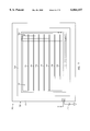
- FIG. 7 is a schematic representation of the upper surface of a flat panel display 700.
- FIG. 8 is a cross sectional view of flat panel display 700 along section line 8--8 of FIG. 7.
- FIG. 9 is a cross sectional view of flat panel display 700 along section line 9--9 of FIG. 7.
- Flat panel display 700 includes spacers 701-707, faceplate structure 720, backplate structure 730, common bus structure 723 and sidewall structure 724.
- Faceplate structure 720 includes insulating faceplate 721 and light emitting structure 722.
- Backplate structure 730 includes insulating backplate 731 and electron emitting structure 732.
- each of spacers 701-707 is identical to spacer 601 (FIG. 6). As illustrated in FIG. 7, spacers 701-707 extend horizontally across light emitting structure 722 in parallel with the pixel rows of flat panel display 700. Light emitting structure 722 defines the viewing surface of flat panel display 700. Common bus structure 723 is laterally separated from this viewing surface. Sidewall structure 724 laterally surrounds the light emitting structure 722 and common bus structure 723.
- sidewall structure 724 extends between faceplate structure 720 and backplate structure 730.
- Light emitting structure 722 of faceplate structure 720 includes a light emissive material 722a, a matrix 722b and a conductive layer 722c.
- Conductive layer 722c extends outside the outer boundary of sidewall structure 724 and is connected to a power supply 740.
- Common bus structure 723 includes an insulating strip 723a and a conductive bus layer 723b. In one embodiment, insulating strip 723a is formed at the same time as matrix 722b, thereby assuring that insulating strip 723a and matrix 722b have substantially the same thickness.
- insulating strip 723a and matrix 722b are formed from polyimide, and have a thickness T of approximately 2 mils. Insulating strip 723a further has a width W of approximately 50 to 100 mils. Conductive layers 722c and 723b can also be formed at the same time. The thicknesses of conductive layers 722c and 723b are negligible with respect to the thicknesses of insulating strip 723a and matrix 722b. Because insulating strip 723a and matrix 722b have approximately the same thickness, conductive layers 722c and 723b are located at the same distance from faceplate 721, thereby facilitating contact between conductive layers 722c and 723b and spacers 701-707.
- spacer 707 includes body 757, edge electrodes 767a, 767b, and 768, face electrodes 777 and 778, and gap 755.
- Spacer 707 is connected between faceplate structure 720 and backplate structure 730 such that conductive layer 722c of light emitting structure 722 contacts edge electrode 767a, conductive bus layer 723b of common bus structure 723 contacts edge electrode 767b, and electron emitting structure 732 of backplate 730 contacts edge electrode 768.
- Gap 755 electrically isolates edge electrodes 767a and 767b.
- Face electrode 777 is electrically connected to edge electrode 767b as illustrated.
- Each of the remaining spacers 701-706 is connected in the same manner as spacer 707.
- spacer 707 could be engaged with a spacer support structure on faceplate structure 720.
- a spacer support structure is not illustrated for purposes of clarity.
- spacer support structures are described in more detail in Spindt, U.S. patent application Ser. Nos. 08,188,855, filed Jan. 31, 1994 now U.S. Pat. No. 5,528,103, and Haven, U.S. patent application Ser. No. 08/343,074, filed Nov. 21, 1994, now U.S. Pat. No. 5,650,690, both of which are hereby incorporated by reference in their entirety.
- each of spacers 701-706 has a corresponding face electrode 771-776 which contacts a corresponding edge electrode 761-766 in the same manner previously described for spacer 707.
- Each of edge electrodes 761-766 contacts conductive bus layer 723b in the same manner as spacer 707.
- conductive bus layer 723b provides a common bus which connects face electrodes 771-777.
- conductive bus structure 723 has a length L of approximately 8 inches.
- spacer 701 will be the first one of spacers 701-707 to be exposed to conditions which could result in spacer charge build-up.
- the common connection of face electrodes 771-777 through conductive bus layer 723b increases the effective capacitance of spacer 701, thereby preventing rapid charge build-up on spacer 701.
- the charge build-up rate on spacers 702-707 is similarly reduced by the common connection of face electrodes 771-777 to conductive bus layer 723b.
- FIG. 10 is a schematic diagram of a flat panel display 1000 in accordance with another embodiment of the present invention. Like the third embodiment, the present embodiment can be used in combination with the previously described first and second embodiments, or independent of these previously described embodiments. Because the flat panel display 1000 illustrated in FIG. 10 is similar to the flat panel display 500 illustrated in FIG. 5, similar elements in FIGS. 5 and 10 are labeled with similar reference numbers.
- FIG. 10 additionally includes external capacitor 1010 which is connected between common bus 504 and ground 1011. Capacitor 1010 increases the effective capacitance of spacers 501-503, thereby further increasing the charging time constant associated with spacers 501-503 and preventing rapid charging of these spacers.
- FIG. 11 is a schematic representation of the upper surface of a flat panel display 1100 in accordance with the present embodiment.
- FIG. 12 is a cross sectional view of flat panel display 1100 along section line 12--12 of FIG. 11. Because flat panel display 1100 is similar to flat panel display 700 (FIGS. 7-9), similar elements in flat panel displays 700 and 1100 are labeled with similar reference numbers.
- flat panel display 1100 additionally includes a common bus extension member 1101 which contacts the conductive bus layer 723b of common bus structure 723. in one variation, common bus extension member 1101 and conductive bus layer 723b are fabricated as a continuous element (See, FIG. 12).
- Bus extension member 1101 extends along faceplate 721 to a location outside of the outer perimeter of sidewall structure 724. External capacitor 1010 is connected to the bus extension member 1101 at a point which is outside the outer perimeter of sidewall structure 724. In this manner, bused face electrodes 771-777 are connected to an external capacitor 1101. This increases the capacitance of spacers 701-707 and prevents fast charge build-up on these spacers.
- FIG. 13 is a schematic diagram of a flat panel display 1300 in accordance with yet another embodiment of the present invention. Like the third and fourth embodiments, the present embodiment can be used in combination with the previously described first and second embodiments, or independent of these previously described embodiments. Because flat panel display 1300 is similar to flat panel display 500 (FIG. 5), similar elements in FIGS. 5 and 13 are labeled with similar reference numbers.
- FIG. 13 additionally includes a capacitor 1310 which is connected between common bus 504 and voltage supply 1311. Capacitor 1310 increases the effective capacitance of spacers 501-503, thereby further increasing the charging time constant associated with spacers 501-503 and preventing rapid charging of these spacers.
- FIG. 14 is a schematic representation of the upper surface of a flat panel display 1400 in accordance with the present embodiment.
- FIG. 15 is a cross sectional view along section line 15--15 of FIG. 14, and
- FIG. 16 is a cross sectional view along section line 16--16 of FIG. 14. Because flat panel display 1400 is similar to flat panel display 700 (FIGS. 7-9), similar elements are labeled with similar reference numbers.
- Flat panel display 1400 includes a capacitor structure 1310 which is fabricated on the interior surface of faceplate 721. As illustrated in FIG. 14, capacitor structure 1310 is located outside of the viewing surface of display 1400 in a location similar to the location of common bus structure 723 (FIG. 7)
- capacitor structure 1310 includes first conductive plate 1301, dielectric layer 1302 and second conductive plate 1303.
- first conductive plate 1301 is continuous with conductive layer 722c of light emitting structure 722. That is, first conductive plate 1301 and conductive layer 722c are deposited at the same time to form a continuous layer of conductive material.
- Dielectric layer 1302 can be, for example, a layer of polyimide having a thickness T of approximately 2 mils, a width W of approximately 50 to 100 mils and a length L of approximately 8 inches.
- Second conductive plate 1303 is deposited on the lower surface of dielectric layer 1302.
- the combined thickness of plates 1301, 1303 and dielectric layer 1302 are selected to be equal to the combined thickness of matrix 722b and conductive layer 722c of light emitting structure 722. As a result, both capacitor structure 1310 and light emitting structure 722 make good-electrical contact with spacers 701-707.
- First and second conductive plates 1301 and 1303 and dielectric layer 1302 form a capacitor.
- the first conductive plate 1301 of this capacitor is connected to voltage supply 1311 through conductive layer 722c of light emitting structure 722 (FIG. 15).
- the second conductive plate 1303 of this capacitor is connected to face electrodes 771-777, such that face electrodes 771-777 extend in parallel from second conductive plate 1303.
- the capacitance of capacitor structure 1310 is determined by the thickness (T), cross sectional area (L ⁇ W), and dielectric constant of dielectric layer 1302. These parameters can be varied to create a capacitor structure 1310 having the desired capacitance. In the described embodiment, capacitor structure 1310 has a capacitance in the range of approximately 3 to 6 nanofarads.
- first conductive plate 1301 is not connected to conductive layer 722c of light emitting structure 722. Instead, first conductive plate 1301 is routed outside the outer perimeter of sidewall structure 724 (See, e.g., extension member 1101 of FIG. 11) and connected to a ground voltage supply.
- FIG. 17 is a schematic representation of the upper surface of a flat panel display 1700 in accordance with another embodiment of the present invention.
- Flat panel display 1700 includes a plurality of spacers 1701-1705 which are disposed perpendicular to (as opposed to in parallel with) the pixel rows. Dashed line 1710 represents one of these pixel rows.
- spacers 1701-1705 As the pixel rows of flat panel display 1700 are activated, each of spacers 1701-1705 is charged at a location which is immediately adjacent to the activated pixel row. For example, when pixel row 1710 is activated, spacers 1701-1705 tend to charge at locations 1701a-1705a.
- FIG. 18 is an isometric view of spacer 1701.
- Spacers 1702-1705 are identical to spacer 1701.
- Spacer 1701 includes spacer body 1711, edge electrodes 1712-1713 and face electrode 1714.
- the various elements of spacer 1701 are substantially identical to the elements of spacer 601, which were previously described in connection with FIG. 6.
- Face electrode 1714 is located approximately halfway up the height of spacer 1701 and extends along the length of spacer body 1711, substantially in parallel with edge electrodes 1712 and 1713.
- face electrode 1714 allows this charge to be distributed (and dissipated) along the length of spacer 1701 as indicated by arrows 1721 and 1722. Consequently, there is no excessive charge build-up along spacers 1701-1705 at locations adjacent to activated pixel rows.
Abstract
Description
              TABLE 1
______________________________________
         Titanium Oxide = 4.0%
         Aluminum Oxide = 32.0%
         Chromium Oxide = 64.0%
______________________________________
              TABLE 2
______________________________________
Aluminum oxide powder 103.7  grams
Chromium oxide powder 207.3  grams
Titanium oxide powder 12.9   grams
Butvar B76            34     grams
Santicizer 150        10     grams
Kellox Z3 Menahden oil
                      0.65   gram
Ethanol               105    grams
Toluene               127    grams
______________________________________
Claims (12)
Priority Applications (1)
| Application Number | Priority Date | Filing Date | Title |
|---|---|---|---|
| US09/161,165 US6064157A (en) | 1996-07-18 | 1998-09-25 | Flat panel display with common bus structure |
Applications Claiming Priority (2)
| Application Number | Priority Date | Filing Date | Title |
|---|---|---|---|
| US08/683,789 US5898266A (en) | 1996-07-18 | 1996-07-18 | Method for displaying frame of pixel information on flat panel display |
| US09/161,165 US6064157A (en) | 1996-07-18 | 1998-09-25 | Flat panel display with common bus structure |
Related Parent Applications (1)
| Application Number | Title | Priority Date | Filing Date |
|---|---|---|---|
| US08/683,789 Division US5898266A (en) | 1996-07-18 | 1996-07-18 | Method for displaying frame of pixel information on flat panel display |
Publications (1)
| Publication Number | Publication Date |
|---|---|
| US6064157A true US6064157A (en) | 2000-05-16 |
Family
ID=24745458
Family Applications (3)
| Application Number | Title | Priority Date | Filing Date |
|---|---|---|---|
| US08/683,789 Expired - Lifetime US5898266A (en) | 1996-07-18 | 1996-07-18 | Method for displaying frame of pixel information on flat panel display |
| US09/161,165 Expired - Lifetime US6064157A (en) | 1996-07-18 | 1998-09-25 | Flat panel display with common bus structure |
| US09/161,069 Expired - Lifetime US6002198A (en) | 1996-07-18 | 1998-09-25 | Flat panel display with spacer of high dielectric constant |
Family Applications Before (1)
| Application Number | Title | Priority Date | Filing Date |
|---|---|---|---|
| US08/683,789 Expired - Lifetime US5898266A (en) | 1996-07-18 | 1996-07-18 | Method for displaying frame of pixel information on flat panel display |
Family Applications After (1)
| Application Number | Title | Priority Date | Filing Date |
|---|---|---|---|
| US09/161,069 Expired - Lifetime US6002198A (en) | 1996-07-18 | 1998-09-25 | Flat panel display with spacer of high dielectric constant |
Country Status (6)
| Country | Link |
|---|---|
| US (3) | US5898266A (en) |
| EP (3) | EP1933358B1 (en) |
| JP (3) | JP3905925B2 (en) |
| KR (1) | KR100401297B1 (en) |
| DE (3) | DE69740032D1 (en) |
| WO (1) | WO1998003986A1 (en) |
Cited By (3)
| Publication number | Priority date | Publication date | Assignee | Title |
|---|---|---|---|---|
| US20030062823A1 (en) * | 2001-09-28 | 2003-04-03 | Candescent Technologies Corporation And Candescent Intellectual Property Services, Inc. | Flat-panel display containing electron-emissive regions of non-uniform spacing or/and multi-part lateral configuration |
| US20070024171A1 (en) * | 2003-08-19 | 2007-02-01 | Tdk Corporation | Spacer for planar panel display, process for producing the same and planar panel display |
| CN100423163C (en) * | 2004-02-17 | 2008-10-01 | Tdk株式会社 | Method for producing spacer for flat panel display |
Families Citing this family (29)
| Publication number | Priority date | Publication date | Assignee | Title |
|---|---|---|---|---|
| JP3187367B2 (en) | 1997-03-31 | 2001-07-11 | キヤノン株式会社 | Electronic device and image forming apparatus using the same |
| US5872424A (en) * | 1997-06-26 | 1999-02-16 | Candescent Technologies Corporation | High voltage compatible spacer coating |
| WO1999034390A1 (en) * | 1997-12-29 | 1999-07-08 | Motorola Inc. | Field emission device having high capacitance spacer |
| US6075323A (en) * | 1998-01-20 | 2000-06-13 | Motorola, Inc. | Method for reducing charge accumulation in a field emission display |
| US6107731A (en) * | 1998-03-31 | 2000-08-22 | Candescent Technologies Corporation | Structure and fabrication of flat-panel display having spacer with laterally segmented face electrode |
| JP3689598B2 (en) | 1998-09-21 | 2005-08-31 | キヤノン株式会社 | Spacer manufacturing method and image forming apparatus manufacturing method using the spacer |
| JP4115050B2 (en) * | 1998-10-07 | 2008-07-09 | キヤノン株式会社 | Electron beam apparatus and spacer manufacturing method |
| US6392334B1 (en) | 1998-10-13 | 2002-05-21 | Micron Technology, Inc. | Flat panel display including capacitor for alignment of baseplate and faceplate |
| US7071907B1 (en) | 1999-05-07 | 2006-07-04 | Candescent Technologies Corporation | Display with active contrast enhancement |
| US6366009B1 (en) | 1999-08-02 | 2002-04-02 | Motorola, Inc. | Method for fabricating a field emission display having a spacer with a passivation layer |
| US6441559B1 (en) | 2000-04-28 | 2002-08-27 | Motorola, Inc. | Field emission display having an invisible spacer and method |
| JP2002157959A (en) | 2000-09-08 | 2002-05-31 | Canon Inc | Method of manufacturing spacer and method of manufacturing image forming device using this spacer |
| US6822626B2 (en) | 2000-10-27 | 2004-11-23 | Science Applications International Corporation | Design, fabrication, testing, and conditioning of micro-components for use in a light-emitting panel |
| US6801001B2 (en) * | 2000-10-27 | 2004-10-05 | Science Applications International Corporation | Method and apparatus for addressing micro-components in a plasma display panel |
| US6796867B2 (en) * | 2000-10-27 | 2004-09-28 | Science Applications International Corporation | Use of printing and other technology for micro-component placement |
| US6620012B1 (en) | 2000-10-27 | 2003-09-16 | Science Applications International Corporation | Method for testing a light-emitting panel and the components therein |
| US6570335B1 (en) * | 2000-10-27 | 2003-05-27 | Science Applications International Corporation | Method and system for energizing a micro-component in a light-emitting panel |
| US7288014B1 (en) | 2000-10-27 | 2007-10-30 | Science Applications International Corporation | Design, fabrication, testing, and conditioning of micro-components for use in a light-emitting panel |
| US6762566B1 (en) | 2000-10-27 | 2004-07-13 | Science Applications International Corporation | Micro-component for use in a light-emitting panel |
| US6545422B1 (en) * | 2000-10-27 | 2003-04-08 | Science Applications International Corporation | Socket for use with a micro-component in a light-emitting panel |
| US6935913B2 (en) * | 2000-10-27 | 2005-08-30 | Science Applications International Corporation | Method for on-line testing of a light emitting panel |
| US6764367B2 (en) * | 2000-10-27 | 2004-07-20 | Science Applications International Corporation | Liquid manufacturing processes for panel layer fabrication |
| US6612889B1 (en) * | 2000-10-27 | 2003-09-02 | Science Applications International Corporation | Method for making a light-emitting panel |
| JP4211323B2 (en) * | 2002-02-27 | 2009-01-21 | 株式会社日立製作所 | Image display device and driving method thereof |
| US20050189164A1 (en) * | 2004-02-26 | 2005-09-01 | Chang Chi L. | Speaker enclosure having outer flared tube |
| JP2006106145A (en) * | 2004-09-30 | 2006-04-20 | Toshiba Corp | Display device |
| US7262548B2 (en) * | 2004-12-15 | 2007-08-28 | Canon Kabushiki Kaisha | Image forming apparatus capable of suppressing a fluctuation in an incident position of an electron beam |
| KR100698408B1 (en) | 2005-07-29 | 2007-03-23 | 학교법인 포항공과대학교 | A spacer structure and method of fabricating the same |
| WO2011042963A1 (en) * | 2009-10-07 | 2011-04-14 | キヤノン株式会社 | Image display device |
Citations (12)
| Publication number | Priority date | Publication date | Assignee | Title |
|---|---|---|---|---|
| US4745332A (en) * | 1986-03-25 | 1988-05-17 | Standard Elektrik Lorenz A. G. | Control plate for picture-reproducing devices |
| US5177410A (en) * | 1990-05-31 | 1993-01-05 | Matsushita Electric Industrial Co., Ltd. | Image display device |
| US5477105A (en) * | 1992-04-10 | 1995-12-19 | Silicon Video Corporation | Structure of light-emitting device with raised black matrix for use in optical devices such as flat-panel cathode-ray tubes |
| US5528103A (en) * | 1994-01-31 | 1996-06-18 | Silicon Video Corporation | Field emitter with focusing ridges situated to sides of gate |
| US5532548A (en) * | 1992-04-10 | 1996-07-02 | Silicon Video Corporation | Field forming electrodes on high voltage spacers |
| US5578899A (en) * | 1994-11-21 | 1996-11-26 | Silicon Video Corporation | Field emission device with internal structure for aligning phosphor pixels with corresponding field emitters |
| US5589731A (en) * | 1992-04-10 | 1996-12-31 | Silicon Video Corporation | Internal support structure for flat panel device |
| US5614781A (en) * | 1992-04-10 | 1997-03-25 | Candescent Technologies Corporation | Structure and operation of high voltage supports |
| US5650690A (en) * | 1994-11-21 | 1997-07-22 | Candescent Technologies, Inc. | Backplate of field emission device with self aligned focus structure and spacer wall locators |
| US5675212A (en) * | 1992-04-10 | 1997-10-07 | Candescent Technologies Corporation | Spacer structures for use in flat panel displays and methods for forming same |
| US5686790A (en) * | 1993-06-22 | 1997-11-11 | Candescent Technologies Corporation | Flat panel device with ceramic backplate |
| US5859502A (en) * | 1996-07-17 | 1999-01-12 | Candescent Technologies Corporation | Spacer locator design for three-dimensional focusing structures in a flat panel display |
Family Cites Families (3)
| Publication number | Priority date | Publication date | Assignee | Title |
|---|---|---|---|---|
| JPH08507643A (en) * | 1993-03-11 | 1996-08-13 | フェド.コーポレイション | Emitter tip structure, field emission device including the emitter tip structure, and method of manufacturing the same |
| JP3251466B2 (en) * | 1994-06-13 | 2002-01-28 | キヤノン株式会社 | Electron beam generator having a plurality of cold cathode elements, driving method thereof, and image forming apparatus using the same |
| CA2196040A1 (en) * | 1994-07-25 | 1996-02-08 | Gary W. Jones | Flat display spacer structure and manufacturing method |
-
1996
- 1996-07-18 US US08/683,789 patent/US5898266A/en not_active Expired - Lifetime
-
1997
- 1997-07-17 EP EP07025233A patent/EP1933358B1/en not_active Expired - Lifetime
- 1997-07-17 JP JP50697898A patent/JP3905925B2/en not_active Expired - Fee Related
- 1997-07-17 DE DE69740032T patent/DE69740032D1/en not_active Expired - Lifetime
- 1997-07-17 DE DE69739198T patent/DE69739198D1/en not_active Expired - Lifetime
- 1997-07-17 EP EP97933337A patent/EP0968510B1/en not_active Expired - Lifetime
- 1997-07-17 WO PCT/US1997/011917 patent/WO1998003986A1/en active IP Right Grant
- 1997-07-17 EP EP06007519A patent/EP1696463B1/en not_active Expired - Lifetime
- 1997-07-17 KR KR10-1999-7000276A patent/KR100401297B1/en not_active IP Right Cessation
- 1997-07-17 DE DE69739826T patent/DE69739826D1/en not_active Expired - Lifetime
-
1998
- 1998-09-25 US US09/161,165 patent/US6064157A/en not_active Expired - Lifetime
- 1998-09-25 US US09/161,069 patent/US6002198A/en not_active Expired - Lifetime
-
2006
- 2006-11-01 JP JP2006298011A patent/JP4461130B2/en not_active Expired - Fee Related
-
2009
- 2009-08-26 JP JP2009195199A patent/JP4457174B2/en not_active Expired - Fee Related
Patent Citations (12)
| Publication number | Priority date | Publication date | Assignee | Title |
|---|---|---|---|---|
| US4745332A (en) * | 1986-03-25 | 1988-05-17 | Standard Elektrik Lorenz A. G. | Control plate for picture-reproducing devices |
| US5177410A (en) * | 1990-05-31 | 1993-01-05 | Matsushita Electric Industrial Co., Ltd. | Image display device |
| US5477105A (en) * | 1992-04-10 | 1995-12-19 | Silicon Video Corporation | Structure of light-emitting device with raised black matrix for use in optical devices such as flat-panel cathode-ray tubes |
| US5532548A (en) * | 1992-04-10 | 1996-07-02 | Silicon Video Corporation | Field forming electrodes on high voltage spacers |
| US5589731A (en) * | 1992-04-10 | 1996-12-31 | Silicon Video Corporation | Internal support structure for flat panel device |
| US5614781A (en) * | 1992-04-10 | 1997-03-25 | Candescent Technologies Corporation | Structure and operation of high voltage supports |
| US5675212A (en) * | 1992-04-10 | 1997-10-07 | Candescent Technologies Corporation | Spacer structures for use in flat panel displays and methods for forming same |
| US5686790A (en) * | 1993-06-22 | 1997-11-11 | Candescent Technologies Corporation | Flat panel device with ceramic backplate |
| US5528103A (en) * | 1994-01-31 | 1996-06-18 | Silicon Video Corporation | Field emitter with focusing ridges situated to sides of gate |
| US5578899A (en) * | 1994-11-21 | 1996-11-26 | Silicon Video Corporation | Field emission device with internal structure for aligning phosphor pixels with corresponding field emitters |
| US5650690A (en) * | 1994-11-21 | 1997-07-22 | Candescent Technologies, Inc. | Backplate of field emission device with self aligned focus structure and spacer wall locators |
| US5859502A (en) * | 1996-07-17 | 1999-01-12 | Candescent Technologies Corporation | Spacer locator design for three-dimensional focusing structures in a flat panel display |
Cited By (5)
| Publication number | Priority date | Publication date | Assignee | Title |
|---|---|---|---|---|
| US20030062823A1 (en) * | 2001-09-28 | 2003-04-03 | Candescent Technologies Corporation And Candescent Intellectual Property Services, Inc. | Flat-panel display containing electron-emissive regions of non-uniform spacing or/and multi-part lateral configuration |
| US6879097B2 (en) | 2001-09-28 | 2005-04-12 | Candescent Technologies Corporation | Flat-panel display containing electron-emissive regions of non-uniform spacing or/and multi-part lateral configuration |
| US20070024171A1 (en) * | 2003-08-19 | 2007-02-01 | Tdk Corporation | Spacer for planar panel display, process for producing the same and planar panel display |
| US7245066B2 (en) | 2003-08-19 | 2007-07-17 | Tdk Corporation | Flat panel display spacer, method of manufacturing flat panel display spacer, and flat panel display |
| CN100423163C (en) * | 2004-02-17 | 2008-10-01 | Tdk株式会社 | Method for producing spacer for flat panel display |
Also Published As
| Publication number | Publication date |
|---|---|
| JP4461130B2 (en) | 2010-05-12 |
| EP0968510B1 (en) | 2010-03-31 |
| JP3905925B2 (en) | 2007-04-18 |
| KR20000067877A (en) | 2000-11-25 |
| DE69739198D1 (en) | 2009-02-12 |
| EP1933358A3 (en) | 2008-07-23 |
| DE69740032D1 (en) | 2010-12-02 |
| EP1933358A2 (en) | 2008-06-18 |
| DE69739826D1 (en) | 2010-05-12 |
| EP1933358B1 (en) | 2010-10-20 |
| JP2007027147A (en) | 2007-02-01 |
| WO1998003986A1 (en) | 1998-01-29 |
| EP1696463B1 (en) | 2008-12-31 |
| EP0968510A1 (en) | 2000-01-05 |
| JP2002515133A (en) | 2002-05-21 |
| JP4457174B2 (en) | 2010-04-28 |
| EP0968510A4 (en) | 2005-01-05 |
| JP2009277671A (en) | 2009-11-26 |
| US5898266A (en) | 1999-04-27 |
| EP1696463A3 (en) | 2006-11-02 |
| EP1696463A2 (en) | 2006-08-30 |
| US6002198A (en) | 1999-12-14 |
| KR100401297B1 (en) | 2003-10-11 |
Similar Documents
| Publication | Publication Date | Title |
|---|---|---|
| US6064157A (en) | Flat panel display with common bus structure | |
| EP0025221B1 (en) | Flat display device | |
| US6441559B1 (en) | Field emission display having an invisible spacer and method | |
| US5872424A (en) | High voltage compatible spacer coating | |
| US5990613A (en) | Field emission device having a non-coated spacer | |
| US5847504A (en) | Field emission display with diode-limited cathode current | |
| US6255771B1 (en) | Flashover control structure for field emitter displays and method of making thereof | |
| EP1603150B1 (en) | Electron emission device and manufacturing method thereof | |
| US20040027050A1 (en) | Black matrix for flat panel field emission displays | |
| US20080048552A1 (en) | Image display device | |
| US7459843B2 (en) | Electron emission device with multilayered insulating layers | |
| JP4457011B2 (en) | Display device having spacer | |
| US20070085463A1 (en) | Electron emission display device | |
| US20060290252A1 (en) | Electron amplification plate for field emission display device | |
| WO1999034390A1 (en) | Field emission device having high capacitance spacer | |
| KR101112705B1 (en) | Segmented conductive coating for a luminescent display device | |
| EP1821329A2 (en) | Electron emission device and electron emission display using the same | |
| JP2795184B2 (en) | Display device | |
| US20080136306A1 (en) | Flat panel display and spacer for use therein | |
| KR20040069528A (en) | Spacer structure of fed panel | |
| JPH10508147A (en) | Field emitter display |
Legal Events
| Date | Code | Title | Description |
|---|---|---|---|
| STCF | Information on status: patent grant |
Free format text: PATENTED CASE |
|
| AS | Assignment |
Owner name: CANDESCENT INTELLECTUAL PROPERTY SERVICES, INC., C Free format text: ASSIGNMENT OF ASSIGNORS INTEREST;ASSIGNOR:CANDESCENT TECHNOLOGIES CORPORATION;REEL/FRAME:011871/0045 Effective date: 20001205 |
|
| FEPP | Fee payment procedure |
Free format text: PAYOR NUMBER ASSIGNED (ORIGINAL EVENT CODE: ASPN); ENTITY STATUS OF PATENT OWNER: LARGE ENTITY |
|
| FPAY | Fee payment |
Year of fee payment: 4 |
|
| AS | Assignment |
Owner name: CANDESCENT TECHNOLOGIES CORPORATION, CALIFORNIA Free format text: CORRECTIVE ASSIGNMENT TO CORRECT THE ASSIGNEES. THE NAME OF AN ASSIGNEE WAS INADVERTENTLY OMITTED FROM THE RECORDATION FORM COVER SHEET PREVIOUSLY RECORDED ON REEL 011871 FRAME 0045;ASSIGNOR:CANDESCENT TECHNOLOGIES CORPORATION;REEL/FRAME:018463/0221 Effective date: 20001205 Owner name: CANDESCENT INTELLECTUAL PROPERTY SERVICES, INC., C Free format text: CORRECTIVE ASSIGNMENT TO CORRECT THE ASSIGNEES. THE NAME OF AN ASSIGNEE WAS INADVERTENTLY OMITTED FROM THE RECORDATION FORM COVER SHEET PREVIOUSLY RECORDED ON REEL 011871 FRAME 0045;ASSIGNOR:CANDESCENT TECHNOLOGIES CORPORATION;REEL/FRAME:018463/0221 Effective date: 20001205 |
|
| AS | Assignment |
Owner name: CANON KABUSHIKI KAISHA, JAPAN Free format text: ASSIGNMENT OF ASSIGNORS INTEREST;ASSIGNOR:CANDESCENT INTELLECTUAL PROPERTY SERVICES, INC.;REEL/FRAME:019035/0114 Effective date: 20060801 |
|
| AS | Assignment |
Owner name: CANON KABUSHIKI KAISHA, JAPAN Free format text: NUNC PRO TUNC ASSIGNMENT;ASSIGNOR:CANDESCENT TECHNOLOGIES CORPORATION;REEL/FRAME:019466/0345 Effective date: 20061207 |
|
| FPAY | Fee payment |
Year of fee payment: 8 |
|
| CC | Certificate of correction | ||
| FPAY | Fee payment |
Year of fee payment: 12 |