US6080677A - Method for preventing micromasking in shallow trench isolation process etching - Google Patents
Method for preventing micromasking in shallow trench isolation process etching Download PDFInfo
- Publication number
- US6080677A US6080677A US09/002,103 US210397A US6080677A US 6080677 A US6080677 A US 6080677A US 210397 A US210397 A US 210397A US 6080677 A US6080677 A US 6080677A
- Authority
- US
- United States
- Prior art keywords
- trench
- substrate
- trench area
- cleaning
- layer
- Prior art date
- Legal status (The legal status is an assumption and is not a legal conclusion. Google has not performed a legal analysis and makes no representation as to the accuracy of the status listed.)
- Expired - Lifetime
Links
- 238000000034 method Methods 0.000 title claims abstract description 38
- 238000002955 isolation Methods 0.000 title claims abstract description 17
- 238000005530 etching Methods 0.000 title claims description 12
- 239000000758 substrate Substances 0.000 claims abstract description 34
- 150000004767 nitrides Chemical class 0.000 claims abstract description 31
- NBVXSUQYWXRMNV-UHFFFAOYSA-N fluoromethane Chemical compound FC NBVXSUQYWXRMNV-UHFFFAOYSA-N 0.000 claims abstract description 6
- 229930195733 hydrocarbon Natural products 0.000 claims abstract description 6
- 150000002430 hydrocarbons Chemical class 0.000 claims abstract description 6
- 239000004215 Carbon black (E152) Substances 0.000 claims abstract description 5
- 239000012535 impurity Substances 0.000 claims abstract description 5
- 239000000126 substance Substances 0.000 claims description 16
- 238000004380 ashing Methods 0.000 claims description 15
- 238000004140 cleaning Methods 0.000 claims description 13
- MHAJPDPJQMAIIY-UHFFFAOYSA-N Hydrogen peroxide Chemical compound OO MHAJPDPJQMAIIY-UHFFFAOYSA-N 0.000 claims description 12
- QAOWNCQODCNURD-UHFFFAOYSA-N Sulfuric acid Chemical compound OS(O)(=O)=O QAOWNCQODCNURD-UHFFFAOYSA-N 0.000 claims description 12
- 239000007789 gas Substances 0.000 claims description 5
- 238000000059 patterning Methods 0.000 claims 1
- XUIMIQQOPSSXEZ-UHFFFAOYSA-N Silicon Chemical compound [Si] XUIMIQQOPSSXEZ-UHFFFAOYSA-N 0.000 description 10
- 229910052710 silicon Inorganic materials 0.000 description 10
- 239000010703 silicon Substances 0.000 description 10
- 229910021420 polycrystalline silicon Inorganic materials 0.000 description 6
- 229920005591 polysilicon Polymers 0.000 description 6
- 238000005229 chemical vapour deposition Methods 0.000 description 5
- QGZKDVFQNNGYKY-UHFFFAOYSA-N Ammonia Chemical compound N QGZKDVFQNNGYKY-UHFFFAOYSA-N 0.000 description 3
- NBIIXXVUZAFLBC-UHFFFAOYSA-N Phosphoric acid Chemical compound OP(O)(O)=O NBIIXXVUZAFLBC-UHFFFAOYSA-N 0.000 description 2
- 230000015572 biosynthetic process Effects 0.000 description 2
- 238000009616 inductively coupled plasma Methods 0.000 description 2
- 238000004518 low pressure chemical vapour deposition Methods 0.000 description 2
- 230000003647 oxidation Effects 0.000 description 2
- 238000007254 oxidation reaction Methods 0.000 description 2
- 239000004065 semiconductor Substances 0.000 description 2
- XLYOFNOQVPJJNP-UHFFFAOYSA-N water Substances O XLYOFNOQVPJJNP-UHFFFAOYSA-N 0.000 description 2
- -1 CHF3 Chemical class 0.000 description 1
- XPDWGBQVDMORPB-UHFFFAOYSA-N Fluoroform Chemical compound FC(F)F XPDWGBQVDMORPB-UHFFFAOYSA-N 0.000 description 1
- XMIJDTGORVPYLW-UHFFFAOYSA-N [SiH2] Chemical compound [SiH2] XMIJDTGORVPYLW-UHFFFAOYSA-N 0.000 description 1
- 229910000147 aluminium phosphate Inorganic materials 0.000 description 1
- 229910021529 ammonia Inorganic materials 0.000 description 1
- 238000009412 basement excavation Methods 0.000 description 1
- 239000000356 contaminant Substances 0.000 description 1
- 230000002950 deficient Effects 0.000 description 1
- 238000000151 deposition Methods 0.000 description 1
- 230000008021 deposition Effects 0.000 description 1
- MROCJMGDEKINLD-UHFFFAOYSA-N dichlorosilane Chemical compound Cl[SiH2]Cl MROCJMGDEKINLD-UHFFFAOYSA-N 0.000 description 1
- 230000001939 inductive effect Effects 0.000 description 1
- 238000004519 manufacturing process Methods 0.000 description 1
- 229910000069 nitrogen hydride Inorganic materials 0.000 description 1
- 238000001020 plasma etching Methods 0.000 description 1
- 238000005498 polishing Methods 0.000 description 1
- 229920000642 polymer Polymers 0.000 description 1
- 238000002360 preparation method Methods 0.000 description 1
Images


Classifications
-
- H—ELECTRICITY
- H01—ELECTRIC ELEMENTS
- H01L—SEMICONDUCTOR DEVICES NOT COVERED BY CLASS H10
- H01L21/00—Processes or apparatus adapted for the manufacture or treatment of semiconductor or solid state devices or of parts thereof
- H01L21/02—Manufacture or treatment of semiconductor devices or of parts thereof
- H01L21/04—Manufacture or treatment of semiconductor devices or of parts thereof the devices having at least one potential-jump barrier or surface barrier, e.g. PN junction, depletion layer or carrier concentration layer
- H01L21/18—Manufacture or treatment of semiconductor devices or of parts thereof the devices having at least one potential-jump barrier or surface barrier, e.g. PN junction, depletion layer or carrier concentration layer the devices having semiconductor bodies comprising elements of Group IV of the Periodic System or AIIIBV compounds with or without impurities, e.g. doping materials
- H01L21/28—Manufacture of electrodes on semiconductor bodies using processes or apparatus not provided for in groups H01L21/20 - H01L21/268
- H01L21/28008—Making conductor-insulator-semiconductor electrodes
- H01L21/28017—Making conductor-insulator-semiconductor electrodes the insulator being formed after the semiconductor body, the semiconductor being silicon
- H01L21/28026—Making conductor-insulator-semiconductor electrodes the insulator being formed after the semiconductor body, the semiconductor being silicon characterised by the conductor
- H01L21/28035—Making conductor-insulator-semiconductor electrodes the insulator being formed after the semiconductor body, the semiconductor being silicon characterised by the conductor the final conductor layer next to the insulator being silicon, e.g. polysilicon, with or without impurities
- H01L21/28044—Making conductor-insulator-semiconductor electrodes the insulator being formed after the semiconductor body, the semiconductor being silicon characterised by the conductor the final conductor layer next to the insulator being silicon, e.g. polysilicon, with or without impurities the conductor comprising at least another non-silicon conductive layer
- H01L21/28052—Making conductor-insulator-semiconductor electrodes the insulator being formed after the semiconductor body, the semiconductor being silicon characterised by the conductor the final conductor layer next to the insulator being silicon, e.g. polysilicon, with or without impurities the conductor comprising at least another non-silicon conductive layer the conductor comprising a silicide layer formed by the silicidation reaction of silicon with a metal layer
-
- H—ELECTRICITY
- H01—ELECTRIC ELEMENTS
- H01L—SEMICONDUCTOR DEVICES NOT COVERED BY CLASS H10
- H01L21/00—Processes or apparatus adapted for the manufacture or treatment of semiconductor or solid state devices or of parts thereof
- H01L21/02—Manufacture or treatment of semiconductor devices or of parts thereof
- H01L21/02041—Cleaning
- H01L21/02043—Cleaning before device manufacture, i.e. Begin-Of-Line process
- H01L21/02052—Wet cleaning only
-
- H—ELECTRICITY
- H01—ELECTRIC ELEMENTS
- H01L—SEMICONDUCTOR DEVICES NOT COVERED BY CLASS H10
- H01L21/00—Processes or apparatus adapted for the manufacture or treatment of semiconductor or solid state devices or of parts thereof
- H01L21/02—Manufacture or treatment of semiconductor devices or of parts thereof
- H01L21/04—Manufacture or treatment of semiconductor devices or of parts thereof the devices having at least one potential-jump barrier or surface barrier, e.g. PN junction, depletion layer or carrier concentration layer
- H01L21/18—Manufacture or treatment of semiconductor devices or of parts thereof the devices having at least one potential-jump barrier or surface barrier, e.g. PN junction, depletion layer or carrier concentration layer the devices having semiconductor bodies comprising elements of Group IV of the Periodic System or AIIIBV compounds with or without impurities, e.g. doping materials
- H01L21/28—Manufacture of electrodes on semiconductor bodies using processes or apparatus not provided for in groups H01L21/20 - H01L21/268
- H01L21/283—Deposition of conductive or insulating materials for electrodes conducting electric current
- H01L21/285—Deposition of conductive or insulating materials for electrodes conducting electric current from a gas or vapour, e.g. condensation
- H01L21/28506—Deposition of conductive or insulating materials for electrodes conducting electric current from a gas or vapour, e.g. condensation of conductive layers
- H01L21/28512—Deposition of conductive or insulating materials for electrodes conducting electric current from a gas or vapour, e.g. condensation of conductive layers on semiconductor bodies comprising elements of Group IV of the Periodic System
- H01L21/28518—Deposition of conductive or insulating materials for electrodes conducting electric current from a gas or vapour, e.g. condensation of conductive layers on semiconductor bodies comprising elements of Group IV of the Periodic System the conductive layers comprising silicides
-
- H—ELECTRICITY
- H01—ELECTRIC ELEMENTS
- H01L—SEMICONDUCTOR DEVICES NOT COVERED BY CLASS H10
- H01L21/00—Processes or apparatus adapted for the manufacture or treatment of semiconductor or solid state devices or of parts thereof
- H01L21/02—Manufacture or treatment of semiconductor devices or of parts thereof
- H01L21/04—Manufacture or treatment of semiconductor devices or of parts thereof the devices having at least one potential-jump barrier or surface barrier, e.g. PN junction, depletion layer or carrier concentration layer
- H01L21/18—Manufacture or treatment of semiconductor devices or of parts thereof the devices having at least one potential-jump barrier or surface barrier, e.g. PN junction, depletion layer or carrier concentration layer the devices having semiconductor bodies comprising elements of Group IV of the Periodic System or AIIIBV compounds with or without impurities, e.g. doping materials
- H01L21/30—Treatment of semiconductor bodies using processes or apparatus not provided for in groups H01L21/20 - H01L21/26
- H01L21/302—Treatment of semiconductor bodies using processes or apparatus not provided for in groups H01L21/20 - H01L21/26 to change their surface-physical characteristics or shape, e.g. etching, polishing, cutting
- H01L21/306—Chemical or electrical treatment, e.g. electrolytic etching
- H01L21/30604—Chemical etching
-
- H—ELECTRICITY
- H01—ELECTRIC ELEMENTS
- H01L—SEMICONDUCTOR DEVICES NOT COVERED BY CLASS H10
- H01L21/00—Processes or apparatus adapted for the manufacture or treatment of semiconductor or solid state devices or of parts thereof
- H01L21/70—Manufacture or treatment of devices consisting of a plurality of solid state components formed in or on a common substrate or of parts thereof; Manufacture of integrated circuit devices or of parts thereof
- H01L21/71—Manufacture of specific parts of devices defined in group H01L21/70
- H01L21/76—Making of isolation regions between components
- H01L21/762—Dielectric regions, e.g. EPIC dielectric isolation, LOCOS; Trench refilling techniques, SOI technology, use of channel stoppers
- H01L21/76224—Dielectric regions, e.g. EPIC dielectric isolation, LOCOS; Trench refilling techniques, SOI technology, use of channel stoppers using trench refilling with dielectric materials
-
- H—ELECTRICITY
- H01—ELECTRIC ELEMENTS
- H01L—SEMICONDUCTOR DEVICES NOT COVERED BY CLASS H10
- H01L29/00—Semiconductor devices adapted for rectifying, amplifying, oscillating or switching, or capacitors or resistors with at least one potential-jump barrier or surface barrier, e.g. PN junction depletion layer or carrier concentration layer; Details of semiconductor bodies or of electrodes thereof ; Multistep manufacturing processes therefor
- H01L29/66—Types of semiconductor device ; Multistep manufacturing processes therefor
- H01L29/66007—Multistep manufacturing processes
- H01L29/66075—Multistep manufacturing processes of devices having semiconductor bodies comprising group 14 or group 13/15 materials
- H01L29/66227—Multistep manufacturing processes of devices having semiconductor bodies comprising group 14 or group 13/15 materials the devices being controllable only by the electric current supplied or the electric potential applied, to an electrode which does not carry the current to be rectified, amplified or switched, e.g. three-terminal devices
- H01L29/66409—Unipolar field-effect transistors
- H01L29/66477—Unipolar field-effect transistors with an insulated gate, i.e. MISFET
- H01L29/665—Unipolar field-effect transistors with an insulated gate, i.e. MISFET using self aligned silicidation, i.e. salicide
-
- H—ELECTRICITY
- H01—ELECTRIC ELEMENTS
- H01L—SEMICONDUCTOR DEVICES NOT COVERED BY CLASS H10
- H01L29/00—Semiconductor devices adapted for rectifying, amplifying, oscillating or switching, or capacitors or resistors with at least one potential-jump barrier or surface barrier, e.g. PN junction depletion layer or carrier concentration layer; Details of semiconductor bodies or of electrodes thereof ; Multistep manufacturing processes therefor
- H01L29/66—Types of semiconductor device ; Multistep manufacturing processes therefor
- H01L29/66007—Multistep manufacturing processes
- H01L29/66075—Multistep manufacturing processes of devices having semiconductor bodies comprising group 14 or group 13/15 materials
- H01L29/66227—Multistep manufacturing processes of devices having semiconductor bodies comprising group 14 or group 13/15 materials the devices being controllable only by the electric current supplied or the electric potential applied, to an electrode which does not carry the current to be rectified, amplified or switched, e.g. three-terminal devices
- H01L29/66409—Unipolar field-effect transistors
- H01L29/66477—Unipolar field-effect transistors with an insulated gate, i.e. MISFET
- H01L29/66568—Lateral single gate silicon transistors
- H01L29/66575—Lateral single gate silicon transistors where the source and drain or source and drain extensions are self-aligned to the sides of the gate
- H01L29/6659—Lateral single gate silicon transistors where the source and drain or source and drain extensions are self-aligned to the sides of the gate with both lightly doped source and drain extensions and source and drain self-aligned to the sides of the gate, e.g. lightly doped drain [LDD] MOSFET, double diffused drain [DDD] MOSFET
Definitions
- the present invention concerns the fabrication of integrated circuits and pertains particularly to a method for preventing micromasking in shallow trench isolation process etching.
- LOCOS local oxidation of silicon
- a layer of pad oxide is formed.
- a layer of nitride is formed on top of the pad oxide.
- the nitride is patterned and etched.
- Field oxide is grown on the substrate at places where the nitride has been etched to expose the substrate. The nitride and pad oxide are then removed.
- Shallow trench isolation is gradually replacing conventional LOCOS process for the formation of an isolation structure as technology is evolving to submicron geometry.
- STI has various advantages over the conventional LOCOS process. For example, STI allows for the planarization of the isolation structure. This results in better control of critical dimension (CD) when defining a gate stack of a transistor. Better control of CD when defining the gate stack results in better control of CD in further processing steps which occur after the gate stack is defined.
- CD critical dimension
- a buffer oxide/nitride mask is patterned onto the silicon wafer to define the trench area.
- a cleaning is performed with wet chemicals such as sulfuric acid and hydrogen peroxide, typically ending with a spin-rinse-dry (SRD).
- the trench area is etched and filled by chemical vapor deposition (CVD) with a fill oxide so that, for an average trench width, local planarization between the trench and the nitride mask is achieved.
- the fill oxide is then polished back by chemical mechanical polishing (CMP) or etched back by dry plasma etch until it is flush with the nitride layer.
- CMP chemical mechanical polishing
- the nitride mask is then removed, leaving the fill oxide extending above the trench.
- the fill oxide is then further removed and a planar surface is provided. This further removal of the fill oxide is done by dry or wet plasma etching of the fill oxide.
- an isolation structure on an integrated circuit is formed using a shallow trench isolation process.
- a layer of buffer oxide is formed on a substrate.
- a layer of nitride is formed on the layer of buffer oxide.
- the layer of nitride and the layer of buffer oxide are patterned to form a trench area.
- the substrate including the trench area is subjected to a plasma comprising H 2 O vapor, and a gaseous fluorocarbon or a fluorinated hydrocarbon gas to clean impurities on the trench area.
- the substrate is etched to form a trench within the trench area.
- CF 4 is introduced into an ashing environment at a flow rate of approximately 180 SCCM.
- H 2 O vapor is then introduced into the ashing environment at a flow rate of approximately 300 SCCM.
- the trench area is cleaned with wet chemicals and a spin rinse dry is performed.
- wet chemicals include sulfuric acid and/or hydrogen peroxide.
- the trench is filled, for example, with a fill oxide.
- a part of the fill oxide is removed so that a remaining part of the fill oxide remaining in the trench is above a top surface of the substrate.
- the nitride layer is then removed.
- the present invention prevents micromasking over a trench area.
- the micromasking resulting from prior art methods can result in leakage sites.
- FIG. 1 is a flowchart for a shallow trench isolation process in accordance with a preferred embodiment of the present invention.
- FIGS. 2, 3, 4, 5, 6 and 7 illustrate the shallow trench isolation process described in FIG. 1 in accordance with a preferred embodiment of the present invention.
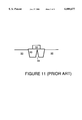
- FIGS. 8, 9, 10 and 11 illustrate how not using the process set out in the flowchart in FIG. 1 can lead to formation of a leakage site.
- FIG. 1 is a flowchart for a shallow trench isolation process in accordance with a preferred embodiment of the present invention.
- a layer of buffer (pad) oxide is formed on a substrate of a semiconductor wafer.
- the layer of buffer oxide is formed by thermal oxidation of silicon to grow the oxide.
- the layer of buffer oxide is, for example, 200 Angstroms ( ⁇ ) thick.
- a layer of nitride is formed on top of the layer of buffer oxide.
- the layer of nitride is, for example, 2000 ⁇ thick.
- the nitride and buffer oxide is patterned by a dry etch process to define a trench area.
- a convention clean of the trench area is performed.
- the clean is performed, for example, with wet chemicals such as sulfuric acid and hydrogen peroxide.
- the clean typically ends with a spin-rinse-dry (SRD).
- a step 25 an additional clean is performed.
- the semiconductor wafer is placed in an ashing environment such as, for example, an inductively coupled plasma.
- an ashing environment such as, for example, an inductively coupled plasma.
- the present invention is also well suited to the use of various other well known ashing environments.
- the ashing environment operates at a pressure of approximately 1.2 Torr and a power of approximately 1000 Watts.
- H 2 O and CF 4 are then introduced into the ashing environment to form an inductively coupled plasma.
- H 2 O is introduced at a flow rate of approximately 300 standard cubic centimeters per minute (SCCM).
- SCCM standard cubic centimeters per minute
- CF 4 is introduced at a flow rate of approximately 180 SCCM.
- gaseous polyfluorocarbons such as C 2 F 6 , or fluorinated hydrocarbons such as CHF 3 , instead of CF 4 , are introduced into the ashing environment at a flow rate of approximately 180 SCCM.
- other flow rates may be used to introduce the gases into the ashing environment.
- other plasma sources such as microwave, can be used in place of the inductive coupled plasma.
- the ashing environment comprising H2 O vapor and the gaseous fluorocarbon or a fluorinated hydrocarbon gas, efficiently and thoroughly removes water spots or polymer contaminants introduced over the trench area into residues.
- FIG. 2 illustrates the result of the completion of step 25.
- sections 32 of a nitride layer are over sections of a buffer oxide layer 31.
- the trench area is clean.
- FIG. 8 illustrates what can happen when step 25 is skipped.
- sections 52 of a nitride layer are over sections of a buffer oxide layer 51.
- An impurity 57 remains on the trench area.
- a trench is formed by, for example performing a dry etch of the silicon wafer.
- the dry etch can be one or more steps to etch the silicon and smooth out the sidewall profile.
- FIG. 3 illustrates the result of the completion of step 26.
- a trench 33 is shown etched in silicon substrate 30.
- trench 33 is 0.5 microns wide and extends 0.4 microns below the surface of substrate 30.
- FIG. 9 illustrates what can happen when step 25 is skipped.
- a trench 53 is shown etched in silicon substrate 50.
- trench 53 is 0.5 microns wide and extends 0.4 microns below the surface of substrate 50.
- a region 58 micromasking has occurred preventing full excavation of the trench.
- a step 27 the trench is filled by chemical vapor deposition (CVD) with a fill oxide so that, for an average trench width, local planarization between the trench and the nitride mask is achieved.
- CVD chemical vapor deposition
- the CVD oxide extends 0.7 micron above the top surface of the nitride layer.
- FIG. 4 illustrates the result of the completion of step 27.
- fill oxide 35 has filled trench 33 (shown in FIG. 3).
- fill oxide 35 extends 0.7 microns above the top surface of the nitride layer 32.
- FIG. 10 illustrates what can happen when step 25 is skipped.
- fill oxide 55 has filled trench 53 (shown in FIG. 9). However, there is no oxide deposited in region 58 where micromasking occurred and the trench was not fully excavated.
- the fill oxide is etched to a level just above the surface of the substrate. This etch is performed, for example, by a combination of chemical mechanical polish (CMP) process and a wet etch.
- CMP chemical mechanical polish
- the amount of fill oxide left above the surface of the substrate is such that future processing steps will remove/etch the remaining fill oxide, such that the remaining fill oxide will be aligned with, or slightly above the surface of the gate oxide.
- FIG. 5 illustrates the result of the completion of step 28.
- fill oxide 35 has been etched to a level just above the top surface of buffer oxide layer 31.
- fill oxide 35 extends 800 ⁇ above the top surface of the buffer layer 31.
- nitride is stripped away, for example, by a wet etch using a "hot" phosphoric acid solution. The result is shown in FIG. 6.
- nitride layer 32 (shown in FIG. 5) is removed.
- FIG. 7 shows a polysilicon region 36 located over fill oxide 35.
- FIG. 11 illustrates what can happen when step 25 is skipped.
- a polysilicon region 56 is located over fill oxide 55. However, there is very little oxide between polysilicon region 56 and region 58 where micromasking occurred. This can result in a leak between the substrate and polysilicon region 56.
Abstract
Description
Claims (18)
Priority Applications (1)
| Application Number | Priority Date | Filing Date | Title |
|---|---|---|---|
| US09/002,103 US6080677A (en) | 1997-06-17 | 1997-12-30 | Method for preventing micromasking in shallow trench isolation process etching |
Applications Claiming Priority (2)
| Application Number | Priority Date | Filing Date | Title |
|---|---|---|---|
| US08/877,095 US5895245A (en) | 1997-06-17 | 1997-06-17 | Plasma ash for silicon surface preparation |
| US09/002,103 US6080677A (en) | 1997-06-17 | 1997-12-30 | Method for preventing micromasking in shallow trench isolation process etching |
Related Parent Applications (1)
| Application Number | Title | Priority Date | Filing Date |
|---|---|---|---|
| US08/877,095 Continuation-In-Part US5895245A (en) | 1997-06-17 | 1997-06-17 | Plasma ash for silicon surface preparation |
Publications (1)
| Publication Number | Publication Date |
|---|---|
| US6080677A true US6080677A (en) | 2000-06-27 |
Family
ID=46254690
Family Applications (1)
| Application Number | Title | Priority Date | Filing Date |
|---|---|---|---|
| US09/002,103 Expired - Lifetime US6080677A (en) | 1997-06-17 | 1997-12-30 | Method for preventing micromasking in shallow trench isolation process etching |
Country Status (1)
| Country | Link |
|---|---|
| US (1) | US6080677A (en) |
Cited By (3)
| Publication number | Priority date | Publication date | Assignee | Title |
|---|---|---|---|---|
| US20040035358A1 (en) * | 2002-08-23 | 2004-02-26 | Cem Basceri | Reactors having gas distributors and methods for depositing materials onto micro-device workpieces |
| US20080233758A1 (en) * | 2007-03-19 | 2008-09-25 | Hynix Semiconductor Inc. | Method for forming trench and method for fabricating semiconductor device using the same |
| US10825717B1 (en) | 2019-07-09 | 2020-11-03 | Nxp B.V. | Method for making high voltage transistors insensitive to needle defects in shallow trench isolation |
Citations (5)
| Publication number | Priority date | Publication date | Assignee | Title |
|---|---|---|---|---|
| US5436190A (en) * | 1994-11-23 | 1995-07-25 | United Microelectronics Corporation | Method for fabricating semiconductor device isolation using double oxide spacers |
| US5445710A (en) * | 1991-01-22 | 1995-08-29 | Kabushiki Kaisha Toshiba | Method of manufacturing semiconductor device |
| US5693147A (en) * | 1995-11-03 | 1997-12-02 | Motorola, Inc. | Method for cleaning a process chamber |
| US5719085A (en) * | 1995-09-29 | 1998-02-17 | Intel Corporation | Shallow trench isolation technique |
| US5879575A (en) * | 1995-11-29 | 1999-03-09 | Applied Materials, Inc. | Self-cleaning plasma processing reactor |
-
1997
- 1997-12-30 US US09/002,103 patent/US6080677A/en not_active Expired - Lifetime
Patent Citations (5)
| Publication number | Priority date | Publication date | Assignee | Title |
|---|---|---|---|---|
| US5445710A (en) * | 1991-01-22 | 1995-08-29 | Kabushiki Kaisha Toshiba | Method of manufacturing semiconductor device |
| US5436190A (en) * | 1994-11-23 | 1995-07-25 | United Microelectronics Corporation | Method for fabricating semiconductor device isolation using double oxide spacers |
| US5719085A (en) * | 1995-09-29 | 1998-02-17 | Intel Corporation | Shallow trench isolation technique |
| US5693147A (en) * | 1995-11-03 | 1997-12-02 | Motorola, Inc. | Method for cleaning a process chamber |
| US5879575A (en) * | 1995-11-29 | 1999-03-09 | Applied Materials, Inc. | Self-cleaning plasma processing reactor |
Cited By (4)
| Publication number | Priority date | Publication date | Assignee | Title |
|---|---|---|---|---|
| US20040035358A1 (en) * | 2002-08-23 | 2004-02-26 | Cem Basceri | Reactors having gas distributors and methods for depositing materials onto micro-device workpieces |
| US20080233758A1 (en) * | 2007-03-19 | 2008-09-25 | Hynix Semiconductor Inc. | Method for forming trench and method for fabricating semiconductor device using the same |
| US7981806B2 (en) * | 2007-03-19 | 2011-07-19 | Hynix Semiconductor Inc. | Method for forming trench and method for fabricating semiconductor device using the same |
| US10825717B1 (en) | 2019-07-09 | 2020-11-03 | Nxp B.V. | Method for making high voltage transistors insensitive to needle defects in shallow trench isolation |
Similar Documents
| Publication | Publication Date | Title |
|---|---|---|
| JP4553410B2 (en) | New shallow trench isolation technology | |
| US6261921B1 (en) | Method of forming shallow trench isolation structure | |
| US6417073B2 (en) | Method for forming element isolating region | |
| US7241665B2 (en) | Shallow trench isolation | |
| US6630390B2 (en) | Method of forming a semiconductor device using a carbon doped oxide layer to control the chemical mechanical polishing of a dielectric layer | |
| CN100495681C (en) | Method for fabricating semiconductor device | |
| US20070111467A1 (en) | Method for forming trench using hard mask with high selectivity and isolation method for semiconductor device using the same | |
| US7611950B2 (en) | Method for forming shallow trench isolation in semiconductor device | |
| US20060148197A1 (en) | Method for forming shallow trench isolation with rounded corners by using a clean process | |
| US6331472B1 (en) | Method for forming shallow trench isolation | |
| US6537914B1 (en) | Integrated circuit device isolation methods using high selectivity chemical-mechanical polishing | |
| US20070161203A1 (en) | Method with high gapfill capability and resulting device structure | |
| US20040018695A1 (en) | Methods of forming trench isolation within a semiconductor substrate | |
| US6248641B1 (en) | Method of fabricating shallow trench isolation | |
| US6080677A (en) | Method for preventing micromasking in shallow trench isolation process etching | |
| US6313007B1 (en) | Semiconductor device, trench isolation structure and methods of formations | |
| US6737359B1 (en) | Method of forming a shallow trench isolation using a sion anti-reflective coating which eliminates water spot defects | |
| KR100758296B1 (en) | Method for forming trench | |
| US6159821A (en) | Methods for shallow trench isolation | |
| US6303467B1 (en) | Method for manufacturing trench isolation | |
| US5498574A (en) | Process of fabricating semiconductor device having flattening stage for inter-level insulating layer without deterioration of device characteristics | |
| US6720235B2 (en) | Method of forming shallow trench isolation in a semiconductor substrate | |
| KR100815036B1 (en) | Isolation method of semiconductor device | |
| KR101127033B1 (en) | Semiconductor Device and Method for Forming STI Type Device Isolation Film of Semiconductor Device | |
| KR100895388B1 (en) | Method for fabricating of semiconductor device |
Legal Events
| Date | Code | Title | Description |
|---|---|---|---|
| AS | Assignment |
Owner name: VLSI TECHNOLOGY, INC., CALIFORNIA Free format text: ASSIGNMENT OF ASSIGNORS INTEREST;ASSIGNORS:GABRIEL, CALVIN;HARVEY, IAN ROBERT;LEARD, LINDA;REEL/FRAME:008953/0631;SIGNING DATES FROM 19971222 TO 19971229 |
|
| FEPP | Fee payment procedure |
Free format text: PAYOR NUMBER ASSIGNED (ORIGINAL EVENT CODE: ASPN); ENTITY STATUS OF PATENT OWNER: LARGE ENTITY |
|
| STCF | Information on status: patent grant |
Free format text: PATENTED CASE |
|
| FPAY | Fee payment |
Year of fee payment: 4 |
|
| AS | Assignment |
Owner name: PHILIPS SEMICONDUCTORS VLSI INC., NEW YORK Free format text: CHANGE OF NAME;ASSIGNOR:VLSI TECHNOLOGY, INC.;REEL/FRAME:018635/0570 Effective date: 19990702 Owner name: NXP B.V., NETHERLANDS Free format text: ASSIGNMENT OF ASSIGNORS INTEREST;ASSIGNOR:PHILIPS SEMICONDUCTORS INC.;REEL/FRAME:018645/0779 Effective date: 20061130 |
|
| AS | Assignment |
Owner name: PHILIPS SEMICONDUCTORS INC., NEW YORK Free format text: CHANGE OF NAME;ASSIGNOR:PHILIPS SEMICONDUCTORS VLSI INC.;REEL/FRAME:018668/0255 Effective date: 19991220 |
|
| FPAY | Fee payment |
Year of fee payment: 8 |
|
| FPAY | Fee payment |
Year of fee payment: 12 |