US6090237A - Apparatus for restraining adhesive overflow in a multilayer substrate assembly during lamination - Google Patents
Apparatus for restraining adhesive overflow in a multilayer substrate assembly during lamination Download PDFInfo
- Publication number
- US6090237A US6090237A US09/013,246 US1324698A US6090237A US 6090237 A US6090237 A US 6090237A US 1324698 A US1324698 A US 1324698A US 6090237 A US6090237 A US 6090237A
- Authority
- US
- United States
- Prior art keywords
- plug
- lamination
- cavity
- layer
- multilayer substrate
- Prior art date
- Legal status (The legal status is an assumption and is not a legal conclusion. Google has not performed a legal analysis and makes no representation as to the accuracy of the status listed.)
- Expired - Fee Related
Links
Images


Classifications
-
- H—ELECTRICITY
- H01—ELECTRIC ELEMENTS
- H01L—SEMICONDUCTOR DEVICES NOT COVERED BY CLASS H10
- H01L21/00—Processes or apparatus adapted for the manufacture or treatment of semiconductor or solid state devices or of parts thereof
- H01L21/02—Manufacture or treatment of semiconductor devices or of parts thereof
- H01L21/04—Manufacture or treatment of semiconductor devices or of parts thereof the devices having at least one potential-jump barrier or surface barrier, e.g. PN junction, depletion layer or carrier concentration layer
- H01L21/48—Manufacture or treatment of parts, e.g. containers, prior to assembly of the devices, using processes not provided for in a single one of the subgroups H01L21/06 - H01L21/326
- H01L21/4814—Conductive parts
- H01L21/4846—Leads on or in insulating or insulated substrates, e.g. metallisation
- H01L21/4857—Multilayer substrates
-
- B—PERFORMING OPERATIONS; TRANSPORTING
- B32—LAYERED PRODUCTS
- B32B—LAYERED PRODUCTS, i.e. PRODUCTS BUILT-UP OF STRATA OF FLAT OR NON-FLAT, e.g. CELLULAR OR HONEYCOMB, FORM
- B32B37/00—Methods or apparatus for laminating, e.g. by curing or by ultrasonic bonding
- B32B37/0007—Methods or apparatus for laminating, e.g. by curing or by ultrasonic bonding involving treatment or provisions in order to avoid deformation or air inclusion, e.g. to improve surface quality
- B32B37/0023—Methods or apparatus for laminating, e.g. by curing or by ultrasonic bonding involving treatment or provisions in order to avoid deformation or air inclusion, e.g. to improve surface quality around holes, apertures or channels present in at least one layer
-
- B—PERFORMING OPERATIONS; TRANSPORTING
- B32—LAYERED PRODUCTS
- B32B—LAYERED PRODUCTS, i.e. PRODUCTS BUILT-UP OF STRATA OF FLAT OR NON-FLAT, e.g. CELLULAR OR HONEYCOMB, FORM
- B32B37/00—Methods or apparatus for laminating, e.g. by curing or by ultrasonic bonding
- B32B37/14—Methods or apparatus for laminating, e.g. by curing or by ultrasonic bonding characterised by the properties of the layers
- B32B37/26—Methods or apparatus for laminating, e.g. by curing or by ultrasonic bonding characterised by the properties of the layers with at least one layer which influences the bonding during the lamination process, e.g. release layers or pressure equalising layers
-
- H—ELECTRICITY
- H01—ELECTRIC ELEMENTS
- H01L—SEMICONDUCTOR DEVICES NOT COVERED BY CLASS H10
- H01L21/00—Processes or apparatus adapted for the manufacture or treatment of semiconductor or solid state devices or of parts thereof
- H01L21/02—Manufacture or treatment of semiconductor devices or of parts thereof
- H01L21/04—Manufacture or treatment of semiconductor devices or of parts thereof the devices having at least one potential-jump barrier or surface barrier, e.g. PN junction, depletion layer or carrier concentration layer
- H01L21/48—Manufacture or treatment of parts, e.g. containers, prior to assembly of the devices, using processes not provided for in a single one of the subgroups H01L21/06 - H01L21/326
- H01L21/4803—Insulating or insulated parts, e.g. mountings, containers, diamond heatsinks
- H01L21/481—Insulating layers on insulating parts, with or without metallisation
-
- H—ELECTRICITY
- H01—ELECTRIC ELEMENTS
- H01L—SEMICONDUCTOR DEVICES NOT COVERED BY CLASS H10
- H01L24/00—Arrangements for connecting or disconnecting semiconductor or solid-state bodies; Methods or apparatus related thereto
- H01L24/01—Means for bonding being attached to, or being formed on, the surface to be connected, e.g. chip-to-package, die-attach, "first-level" interconnects; Manufacturing methods related thereto
- H01L24/42—Wire connectors; Manufacturing methods related thereto
- H01L24/47—Structure, shape, material or disposition of the wire connectors after the connecting process
- H01L24/49—Structure, shape, material or disposition of the wire connectors after the connecting process of a plurality of wire connectors
-
- H—ELECTRICITY
- H05—ELECTRIC TECHNIQUES NOT OTHERWISE PROVIDED FOR
- H05K—PRINTED CIRCUITS; CASINGS OR CONSTRUCTIONAL DETAILS OF ELECTRIC APPARATUS; MANUFACTURE OF ASSEMBLAGES OF ELECTRICAL COMPONENTS
- H05K3/00—Apparatus or processes for manufacturing printed circuits
- H05K3/46—Manufacturing multilayer circuits
- H05K3/4697—Manufacturing multilayer circuits having cavities, e.g. for mounting components
-
- H—ELECTRICITY
- H01—ELECTRIC ELEMENTS
- H01L—SEMICONDUCTOR DEVICES NOT COVERED BY CLASS H10
- H01L2223/00—Details relating to semiconductor or other solid state devices covered by the group H01L23/00
- H01L2223/544—Marks applied to semiconductor devices or parts
- H01L2223/54406—Marks applied to semiconductor devices or parts comprising alphanumeric information
-
- H—ELECTRICITY
- H01—ELECTRIC ELEMENTS
- H01L—SEMICONDUCTOR DEVICES NOT COVERED BY CLASS H10
- H01L2223/00—Details relating to semiconductor or other solid state devices covered by the group H01L23/00
- H01L2223/544—Marks applied to semiconductor devices or parts
- H01L2223/54473—Marks applied to semiconductor devices or parts for use after dicing
- H01L2223/54486—Located on package parts, e.g. encapsulation, leads, package substrate
-
- H—ELECTRICITY
- H01—ELECTRIC ELEMENTS
- H01L—SEMICONDUCTOR DEVICES NOT COVERED BY CLASS H10
- H01L2224/00—Indexing scheme for arrangements for connecting or disconnecting semiconductor or solid-state bodies and methods related thereto as covered by H01L24/00
- H01L2224/01—Means for bonding being attached to, or being formed on, the surface to be connected, e.g. chip-to-package, die-attach, "first-level" interconnects; Manufacturing methods related thereto
- H01L2224/42—Wire connectors; Manufacturing methods related thereto
- H01L2224/47—Structure, shape, material or disposition of the wire connectors after the connecting process
- H01L2224/48—Structure, shape, material or disposition of the wire connectors after the connecting process of an individual wire connector
- H01L2224/4805—Shape
- H01L2224/4809—Loop shape
- H01L2224/48095—Kinked
-
- H—ELECTRICITY
- H01—ELECTRIC ELEMENTS
- H01L—SEMICONDUCTOR DEVICES NOT COVERED BY CLASS H10
- H01L2224/00—Indexing scheme for arrangements for connecting or disconnecting semiconductor or solid-state bodies and methods related thereto as covered by H01L24/00
- H01L2224/01—Means for bonding being attached to, or being formed on, the surface to be connected, e.g. chip-to-package, die-attach, "first-level" interconnects; Manufacturing methods related thereto
- H01L2224/42—Wire connectors; Manufacturing methods related thereto
- H01L2224/47—Structure, shape, material or disposition of the wire connectors after the connecting process
- H01L2224/48—Structure, shape, material or disposition of the wire connectors after the connecting process of an individual wire connector
- H01L2224/481—Disposition
- H01L2224/48151—Connecting between a semiconductor or solid-state body and an item not being a semiconductor or solid-state body, e.g. chip-to-substrate, chip-to-passive
- H01L2224/48221—Connecting between a semiconductor or solid-state body and an item not being a semiconductor or solid-state body, e.g. chip-to-substrate, chip-to-passive the body and the item being stacked
- H01L2224/48225—Connecting between a semiconductor or solid-state body and an item not being a semiconductor or solid-state body, e.g. chip-to-substrate, chip-to-passive the body and the item being stacked the item being non-metallic, e.g. insulating substrate with or without metallisation
- H01L2224/48227—Connecting between a semiconductor or solid-state body and an item not being a semiconductor or solid-state body, e.g. chip-to-substrate, chip-to-passive the body and the item being stacked the item being non-metallic, e.g. insulating substrate with or without metallisation connecting the wire to a bond pad of the item
-
- H—ELECTRICITY
- H01—ELECTRIC ELEMENTS
- H01L—SEMICONDUCTOR DEVICES NOT COVERED BY CLASS H10
- H01L2224/00—Indexing scheme for arrangements for connecting or disconnecting semiconductor or solid-state bodies and methods related thereto as covered by H01L24/00
- H01L2224/01—Means for bonding being attached to, or being formed on, the surface to be connected, e.g. chip-to-package, die-attach, "first-level" interconnects; Manufacturing methods related thereto
- H01L2224/42—Wire connectors; Manufacturing methods related thereto
- H01L2224/47—Structure, shape, material or disposition of the wire connectors after the connecting process
- H01L2224/48—Structure, shape, material or disposition of the wire connectors after the connecting process of an individual wire connector
- H01L2224/484—Connecting portions
- H01L2224/48463—Connecting portions the connecting portion on the bonding area of the semiconductor or solid-state body being a ball bond
- H01L2224/48465—Connecting portions the connecting portion on the bonding area of the semiconductor or solid-state body being a ball bond the other connecting portion not on the bonding area being a wedge bond, i.e. ball-to-wedge, regular stitch
-
- H—ELECTRICITY
- H01—ELECTRIC ELEMENTS
- H01L—SEMICONDUCTOR DEVICES NOT COVERED BY CLASS H10
- H01L2224/00—Indexing scheme for arrangements for connecting or disconnecting semiconductor or solid-state bodies and methods related thereto as covered by H01L24/00
- H01L2224/01—Means for bonding being attached to, or being formed on, the surface to be connected, e.g. chip-to-package, die-attach, "first-level" interconnects; Manufacturing methods related thereto
- H01L2224/42—Wire connectors; Manufacturing methods related thereto
- H01L2224/47—Structure, shape, material or disposition of the wire connectors after the connecting process
- H01L2224/49—Structure, shape, material or disposition of the wire connectors after the connecting process of a plurality of wire connectors
- H01L2224/491—Disposition
- H01L2224/49105—Connecting at different heights
- H01L2224/49109—Connecting at different heights outside the semiconductor or solid-state body
-
- H—ELECTRICITY
- H01—ELECTRIC ELEMENTS
- H01L—SEMICONDUCTOR DEVICES NOT COVERED BY CLASS H10
- H01L24/00—Arrangements for connecting or disconnecting semiconductor or solid-state bodies; Methods or apparatus related thereto
- H01L24/01—Means for bonding being attached to, or being formed on, the surface to be connected, e.g. chip-to-package, die-attach, "first-level" interconnects; Manufacturing methods related thereto
- H01L24/42—Wire connectors; Manufacturing methods related thereto
- H01L24/47—Structure, shape, material or disposition of the wire connectors after the connecting process
- H01L24/48—Structure, shape, material or disposition of the wire connectors after the connecting process of an individual wire connector
-
- H—ELECTRICITY
- H01—ELECTRIC ELEMENTS
- H01L—SEMICONDUCTOR DEVICES NOT COVERED BY CLASS H10
- H01L2924/00—Indexing scheme for arrangements or methods for connecting or disconnecting semiconductor or solid-state bodies as covered by H01L24/00
- H01L2924/0001—Technical content checked by a classifier
- H01L2924/00014—Technical content checked by a classifier the subject-matter covered by the group, the symbol of which is combined with the symbol of this group, being disclosed without further technical details
-
- H—ELECTRICITY
- H01—ELECTRIC ELEMENTS
- H01L—SEMICONDUCTOR DEVICES NOT COVERED BY CLASS H10
- H01L2924/00—Indexing scheme for arrangements or methods for connecting or disconnecting semiconductor or solid-state bodies as covered by H01L24/00
- H01L2924/01—Chemical elements
- H01L2924/01013—Aluminum [Al]
-
- H—ELECTRICITY
- H01—ELECTRIC ELEMENTS
- H01L—SEMICONDUCTOR DEVICES NOT COVERED BY CLASS H10
- H01L2924/00—Indexing scheme for arrangements or methods for connecting or disconnecting semiconductor or solid-state bodies as covered by H01L24/00
- H01L2924/01—Chemical elements
- H01L2924/01028—Nickel [Ni]
-
- H—ELECTRICITY
- H01—ELECTRIC ELEMENTS
- H01L—SEMICONDUCTOR DEVICES NOT COVERED BY CLASS H10
- H01L2924/00—Indexing scheme for arrangements or methods for connecting or disconnecting semiconductor or solid-state bodies as covered by H01L24/00
- H01L2924/01—Chemical elements
- H01L2924/01029—Copper [Cu]
-
- H—ELECTRICITY
- H01—ELECTRIC ELEMENTS
- H01L—SEMICONDUCTOR DEVICES NOT COVERED BY CLASS H10
- H01L2924/00—Indexing scheme for arrangements or methods for connecting or disconnecting semiconductor or solid-state bodies as covered by H01L24/00
- H01L2924/01—Chemical elements
- H01L2924/01075—Rhenium [Re]
-
- H—ELECTRICITY
- H01—ELECTRIC ELEMENTS
- H01L—SEMICONDUCTOR DEVICES NOT COVERED BY CLASS H10
- H01L2924/00—Indexing scheme for arrangements or methods for connecting or disconnecting semiconductor or solid-state bodies as covered by H01L24/00
- H01L2924/01—Chemical elements
- H01L2924/01078—Platinum [Pt]
-
- H—ELECTRICITY
- H01—ELECTRIC ELEMENTS
- H01L—SEMICONDUCTOR DEVICES NOT COVERED BY CLASS H10
- H01L2924/00—Indexing scheme for arrangements or methods for connecting or disconnecting semiconductor or solid-state bodies as covered by H01L24/00
- H01L2924/01—Chemical elements
- H01L2924/01079—Gold [Au]
-
- H—ELECTRICITY
- H01—ELECTRIC ELEMENTS
- H01L—SEMICONDUCTOR DEVICES NOT COVERED BY CLASS H10
- H01L2924/00—Indexing scheme for arrangements or methods for connecting or disconnecting semiconductor or solid-state bodies as covered by H01L24/00
- H01L2924/013—Alloys
- H01L2924/014—Solder alloys
-
- H—ELECTRICITY
- H01—ELECTRIC ELEMENTS
- H01L—SEMICONDUCTOR DEVICES NOT COVERED BY CLASS H10
- H01L2924/00—Indexing scheme for arrangements or methods for connecting or disconnecting semiconductor or solid-state bodies as covered by H01L24/00
- H01L2924/15—Details of package parts other than the semiconductor or other solid state devices to be connected
- H01L2924/151—Die mounting substrate
- H01L2924/1515—Shape
- H01L2924/15153—Shape the die mounting substrate comprising a recess for hosting the device
-
- H—ELECTRICITY
- H01—ELECTRIC ELEMENTS
- H01L—SEMICONDUCTOR DEVICES NOT COVERED BY CLASS H10
- H01L2924/00—Indexing scheme for arrangements or methods for connecting or disconnecting semiconductor or solid-state bodies as covered by H01L24/00
- H01L2924/15—Details of package parts other than the semiconductor or other solid state devices to be connected
- H01L2924/151—Die mounting substrate
- H01L2924/1517—Multilayer substrate
-
- H—ELECTRICITY
- H01—ELECTRIC ELEMENTS
- H01L—SEMICONDUCTOR DEVICES NOT COVERED BY CLASS H10
- H01L2924/00—Indexing scheme for arrangements or methods for connecting or disconnecting semiconductor or solid-state bodies as covered by H01L24/00
- H01L2924/15—Details of package parts other than the semiconductor or other solid state devices to be connected
- H01L2924/151—Die mounting substrate
- H01L2924/153—Connection portion
- H01L2924/1532—Connection portion the connection portion being formed on the die mounting surface of the substrate
- H01L2924/1533—Connection portion the connection portion being formed on the die mounting surface of the substrate the connection portion being formed both on the die mounting surface of the substrate and outside the die mounting surface of the substrate
- H01L2924/15331—Connection portion the connection portion being formed on the die mounting surface of the substrate the connection portion being formed both on the die mounting surface of the substrate and outside the die mounting surface of the substrate being a ball array, e.g. BGA
-
- H—ELECTRICITY
- H01—ELECTRIC ELEMENTS
- H01L—SEMICONDUCTOR DEVICES NOT COVERED BY CLASS H10
- H01L2924/00—Indexing scheme for arrangements or methods for connecting or disconnecting semiconductor or solid-state bodies as covered by H01L24/00
- H01L2924/30—Technical effects
- H01L2924/301—Electrical effects
- H01L2924/3011—Impedance
-
- H—ELECTRICITY
- H05—ELECTRIC TECHNIQUES NOT OTHERWISE PROVIDED FOR
- H05K—PRINTED CIRCUITS; CASINGS OR CONSTRUCTIONAL DETAILS OF ELECTRIC APPARATUS; MANUFACTURE OF ASSEMBLAGES OF ELECTRICAL COMPONENTS
- H05K1/00—Printed circuits
- H05K1/18—Printed circuits structurally associated with non-printed electric components
- H05K1/182—Printed circuits structurally associated with non-printed electric components associated with components mounted in the printed circuit board, e.g. insert mounted components [IMC]
- H05K1/183—Components mounted in and supported by recessed areas of the printed circuit board
-
- H—ELECTRICITY
- H05—ELECTRIC TECHNIQUES NOT OTHERWISE PROVIDED FOR
- H05K—PRINTED CIRCUITS; CASINGS OR CONSTRUCTIONAL DETAILS OF ELECTRIC APPARATUS; MANUFACTURE OF ASSEMBLAGES OF ELECTRICAL COMPONENTS
- H05K2201/00—Indexing scheme relating to printed circuits covered by H05K1/00
- H05K2201/01—Dielectrics
- H05K2201/0104—Properties and characteristics in general
- H05K2201/0133—Elastomeric or compliant polymer
-
- H—ELECTRICITY
- H05—ELECTRIC TECHNIQUES NOT OTHERWISE PROVIDED FOR
- H05K—PRINTED CIRCUITS; CASINGS OR CONSTRUCTIONAL DETAILS OF ELECTRIC APPARATUS; MANUFACTURE OF ASSEMBLAGES OF ELECTRICAL COMPONENTS
- H05K2201/00—Indexing scheme relating to printed circuits covered by H05K1/00
- H05K2201/09—Shape and layout
- H05K2201/09818—Shape or layout details not covered by a single group of H05K2201/09009 - H05K2201/09809
- H05K2201/09845—Stepped hole, via, edge, bump or conductor
-
- H—ELECTRICITY
- H05—ELECTRIC TECHNIQUES NOT OTHERWISE PROVIDED FOR
- H05K—PRINTED CIRCUITS; CASINGS OR CONSTRUCTIONAL DETAILS OF ELECTRIC APPARATUS; MANUFACTURE OF ASSEMBLAGES OF ELECTRICAL COMPONENTS
- H05K3/00—Apparatus or processes for manufacturing printed circuits
- H05K3/46—Manufacturing multilayer circuits
- H05K3/4611—Manufacturing multilayer circuits by laminating two or more circuit boards
-
- Y—GENERAL TAGGING OF NEW TECHNOLOGICAL DEVELOPMENTS; GENERAL TAGGING OF CROSS-SECTIONAL TECHNOLOGIES SPANNING OVER SEVERAL SECTIONS OF THE IPC; TECHNICAL SUBJECTS COVERED BY FORMER USPC CROSS-REFERENCE ART COLLECTIONS [XRACs] AND DIGESTS
- Y10—TECHNICAL SUBJECTS COVERED BY FORMER USPC
- Y10T—TECHNICAL SUBJECTS COVERED BY FORMER US CLASSIFICATION
- Y10T29/00—Metal working
- Y10T29/49—Method of mechanical manufacture
- Y10T29/49002—Electrical device making
- Y10T29/49117—Conductor or circuit manufacturing
- Y10T29/49124—On flat or curved insulated base, e.g., printed circuit, etc.
- Y10T29/49155—Manufacturing circuit on or in base
- Y10T29/49158—Manufacturing circuit on or in base with molding of insulated base
Definitions
- the invention relates generally to packages for semiconductor devices, and more particularly to a method of making a multilayer substrate suitable for such packages.
- Many high performance semiconductor packages incorporate a multilayer substrate, with an interior cavity, for interconnection with a semiconductor device.
- the semiconductor device is located within the interior cavity where it is electrically connected to each of a plurality of wiring layers in the multilayer substrate.
- Each wiring layer comprises a fiberglass laminate bonded on either side to a layer of metal, e.g., copper, defining an interconnection circuitry pattern.
- the interior cavity has a stepped vertical profile and each step, or bonding tier, includes bonding surfaces, or bond pads, for accepting wire bond connections from the semiconductor device.
- a multilayer substrate may be produced by laminating, i.e., bonding, an assembly comprised of several wiring layers, each layer having a differently sized interior cavity or window, stacked so that the assembly has an interior cavity with a stepped vertical profile.
- One or more layers of adhesive usually in the form of a sheet of woven material coated with a partially cured epoxy resin, or "pre preg," are interposed between adjacent wiring layers and bond the layers together during lamination.
- One solution proposed is to prevent adhesive overflow onto the bonding tiers by coating the adjacent surfaces of two wiring layers in the lamination assembly with a layer of epoxy resin prior to lamination.
- a thinner sheet of pre preg may be used between adjacent wiring layers and the edge of the sheet may be recessed from the edge of the larger interior window of the upper wiring layer with the pre-coated epoxy resin providing adhesive material at that edge.
- a problem that may be encountered in the manufacture of a high performance semiconductor package that includes a multilayer substrate is adhesion at the nonessential metal surfaces in the cavity, i.e., those metal surfaces not required for wire bonding.
- the interior cavity of the multilayer substrate, which houses the semiconductor device may be encapsulated for environmental protection using a liquid epoxy resin or other components may be bonded onto the cavity surface using polymer adhesives.
- These adhesives or encapsulants usually have a low bonding affinity for metal, e.g., the metal surfaces on the vertical edges of the wiring layers.
- Resin dust refers to particles and fibers which dislodge from the fiberglass laminates in the wiring and adhesive layers and migrate throughout the assembly during lamination. This resin dust may adhere to the bond pads, decreasing the integrity of the ultimate electrical connection between the wire bonds on the semiconductor device and the bond pads on the package.
- the present invention provides a way to reduce adhesive overflow onto the bonding tiers of a multilayer substrate during lamination without introducing additional materials into the substrate.
- the invention also provides a smooth or micro patterned surface to adhesive exposed in the cavity of the multilayer substrate.
- the invention reduces resin dust contamination of the bond pads in the cavity of the multilayer substrate during lamination.
- the flow of adhesive in a multilayer assembly is restrained during lamination, i.e., bonding. More particularly, the flow of adhesive is restrained by inserting a plug into the interior cavity having a shape configured to mate with the stepped profile of the interior cavity.
- the plug is made of an elastomeric material.
- the plug is sized to provide a limited space between the plug and the wiring layers to permit adhesive to flow into and fill the space between the plug and the vertical edges of respective wiring layers.
- the adhesive conforms to the shape defined by the space, thereby coating the metal surface on the vertical edges of the wiring layers without coating the portions of the wiring layer which should remain uncoated.
- the plug includes a layer of a material harder than the material of the plug in contact with the stepped profile of the interior cavity to facilitate removal of the plug without damaging the wire bonding sites on the surfaces of the wiring layers exposed in the cavity.
- the metallic bonding surface of the multilayer substrate assembly is advantageously coated with a layer of a photo sensitive material prior to lamination to protect the metallic bonding surfaces of the interior cavity from damage due to pressure exerted by the plug during lamination.
- the photo sensitive layer also prevents contamination of the metallic bonding surfaces due to particulate migration during lamination.
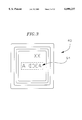
- FIG. 1 is a top view of a high performance ball grid array (“BGA”) semiconductor device package including a multilayer substrate with an interior cavity;
- BGA ball grid array
- FIG. 2 is a partial cross-sectional view of the BGA package
- FIG. 3 is a bottom view of the plug
- FIG. 4 is a side view of the plug
- FIG. 5 is a partial cross-sectional view of the plug placed in the interior cavity of the lamination assembly
- FIG. 6 is a partial cross-sectional view of the meniscus formed between wiring layers by one version of the plug
- FIG. 7 is a partial cross-sectional view depicting another embodiment of the plug.
- FIG. 8A is a partial cross-sectional view of the meniscus formed between wiring layers by another version of the plug.
- FIG. 8B is a view similar to FIG. 8A, but depicting the meniscus formed between wiring layers by yet another version of the plug;
- FIG. 9 is a view similar to FIG. 7, but depicting yet another embodiment of the plug.
- FIG. 10 is a schematic showing a tool for removing the plug
- FIG. 11A is a cross-sectional view of a lamination layer having a plurality of attached plugs
- FIG. 11B is a view similar to FIG. 11A, but depicting another version of the lamination layer including a plurality of plugs;
- FIG. 12 is a partial cross-sectional view of the plug placed in the interior cavity of a multilayer substrate positioned on the heat slug.
- FIG. 13 is a partial cross-sectional view of the interior cavity of the lamination assembly coated with a protective layer of photo sensitive material.
- FIG. 1 illustrates a ball grid array (“BGA") semiconductor package 14, an example of one type of single chip semiconductor package which includes a multilayer substrate 15.
- BGA ball grid array
- the multilayer substrate includes an interior cavity having a stepped vertical profile and is mounted in the BGA package to a metal plate 16, or heat slug, to which a semiconductor device 17 is mounted, as shown in FIG. 2.
- the heat slug provides a mounting surface for the semiconductor device in the interior cavity and also acts as a heat sink to dissipate heat generated by the device during operation.
- An array of solder balls 18 is provided on the exterior surface of the package to accommodate electrical interconnection with other devices.
- the multilayer substrate consists of a plurality, i.e., two or more, stacked wiring layers 20, each wiring layer including a window portion.
- Each wiring layer comprises a fiberglass laminate bonded on either side to a layer of metal, e.g., copper, defining an interconnection circuitry pattern.
- the interior cavity of the assembly is formed by stacking wiring layers with increasingly larger window portions.
- Each wiring layer has a step portion 22 exposed in the cavity, the bonding tier, or step, which includes bond pads 24 for wire bonding.
- Wire bonds 26 are attached at one end to the leads on semiconductor device 17 and to corresponding bond pads 24 at the other end to interconnect the device and the package.
- Each bond pad is in turn electrically connected to another bond pad or to one corresponding solder ball on the exterior of the BGA package.
- the multilayer substrate enables the interconnection of one semiconductor device to several wiring levels, providing the high interconnection density and control of electrical characteristics required for high performance applications.
- the multilayer substrate is formed by laminating an assembly comprising several stacked wiring layers with a layer of adhesive 28, e.g., a film of a partially cured epoxy or cyanate ester resin, or "pre preg," interposed between adjacent wiring layers during lamination.
- the adhesive layer may also be a sheet of woven material coated with a pre preg resin.
- the edge of the adhesive layer may be flush with the edge of the window portion of the upper wiring layer (see FIG. 5) or slightly recessed.
- the stacked wiring layers are sandwiched between a first lamination layer 30 and a second lamination layer 32.
- these layers each comprise a fiberglass laminate having an outer side 33, 34 coated with a layer of copper foil and an inner side 35, 36 adjacent a wiring layer.
- a layer of adhesive is interposed between the inner sides of the lamination layers and the adjacent wiring layers.
- the heat and pressure of the lamination process cause the adhesive to melt and flow between adjacent layers and then cure and bond the layers together into a multilayer structure.
- portions of first lamination layer 30 and second lamination layer 32 are routed or otherwise removed to expose the interior cavity of the multilayer substrate.
- the lamination layers may also be rigid sheets, e.g., of copper or polymeric material, coated with a layer of elastomeric material directly contacting the outer wiring layers of the multilayer assembly, which are completely removed after lamination.
- FIG. 3 illustrates a plug 40 provided to restrain the flow of adhesive in the interior cavity of a multilayer substrate during lamination.
- the plug is formed entirely of an elastomeric material, e.g., silicone, having a preferred hardness of 60 to 70 durometers.
- the plug includes a stepped vertical profile 42, as shown in FIG. 4, shaped to mate, i.e., conform, with the stepped vertical profile of the interior cavity of the multilayer substrate.
- the plug includes a bottom surface 44 and a top surface 46.
- FIG. 5 shows a partial cross-sectional view of the plug in mating position with the interior cavity of the multilayer substrate prior to lamination.
- Each step of the vertical profile of the plug includes a horizontal face 48 adjacent a horizontal surface of a bonding tier, a vertical edge 50 adjacent a vertical edge of a bonding tier and a corner 52 placed adjacent an adhesive layer 28 between two wiring layers 20 in the lamination assembly.
- the corners may have curved or chamfered surfaces (see FIGS. 5, 7 and 9).
- Adhesive flowing from between the wiring layers onto bonding tiers 22 in the interior cavity of the multilayer substrate effectively decreases the bondable metal surface of each bond pad on the bonding tier. Accordingly, it is desirable to build in tolerances for such adhesive overflow by increasing the width of each bonding tier in the multilayer substrate.
- the width of each bonding tier can be reduced. This reduces the requisite length of wire bonds between the semiconductor device and the bond pads in the cavity of the multilayer substrate.
- signal speed is inversely proportional to wire bond lengths
- reducing wire bond lengths advantageously increases signal speeds in, and overall performance of the package.
- adhesive material on the bonding tiers 22 resulting from adhesive overflow during lamination tends to have a rough surface which may capture chemicals and moisture during subsequent processing steps, ruining the semiconductor package.
- Plug 40 advantageously restricts adhesive flowing from between the wiring layers onto bonding tiers 22 and molds it into a desired shape.
- adhesive overflow is restricted by the stepped vertical profile of the plug, including at corners 52.
- the topography of the adhesive material exposed in the cavity conforms to the topography of the plug surface, and may be smooth or micro patterned.
- Controlled adhesive overflow onto the vertical or horizontal surfaces of the interior layer may be desirable in some applications. For example, it may be desirable to bond other components onto the cavity surface of the BGA using polymer adhesives or to encapsulate the semiconductor device in the cavity with an encapsulant ("glob top"), e.g., liquid epoxy, for environmental protection or performance and reliability enhancement of the semiconductor device and package.
- an encapsulant e.g., liquid epoxy
- These adhesives have a low bonding affinity for metal surfaces and may make it desirable to minimize nonessential metal surfaces in the cavity, in particular, the metal surfaces on the vertical edges of the wiring layer which are not used for wire bonding. Directing adhesive overflow onto these surfaces reduces the area of exposed metal surfaces in the cavity. This may be accomplished according to one embodiment of the invention shown in FIG. 7.
- the stepped vertical profile of the plug has a vertical edge including a surface 55 that contacts the vertical edge of the adjacent wiring layer and a recessed portion 56 adjacent to one of the corners.
- adhesive flows between the wiring layer and is restricted by corner 52.
- the adhesive then flows into recessed portion 56, covering a portion of vertical edge of the adjacent wiring layer, and is then restricted by a bottom shelf 57 of contact portion 55.
- the exposed metal surface area on the vertical edges of the resultant multilayer substrate is thereby minimized, as shown in FIG. 8A, providing an improved surface for accommodating an encapsulant and/or other polymer adhesives.
- Recessed portion 56 may also be made flush with the horizontal face of the step 22, which allows adhesive to coat the entire vertical edge of the adjacent wiring layer.
- the plug may also be shaped to allow adhesive flow to extend slightly onto the horizontal face of the wiring layer, resulting in an adhesive layer wrapped slightly over the edge of the wiring layer, as shown in FIG. 8B. Extending the adhesive up to or over the vertical edge of the wiring layers in this manner also makes it easier to visually verify the formation of a good meniscus at the junctions between the wiring layers.
- FIG. 7 also illustrates a further embodiment of the plug which includes a core 58 of a relatively hard material, e.g., aluminum, steel or a hard polymer, surrounded by a layer of silicone 60 with a hardness in the preferred range of 40 to 80 durometers at the stepped vertical profile.
- a relatively hard material e.g., aluminum, steel or a hard polymer
- silicone 60 with a hardness in the preferred range of 40 to 80 durometers at the stepped vertical profile.
- the hard core offers increased support to the stepped vertical profile of the plug for restricting adhesive flow during lamination.
- the appropriate durometer of silicone layer 60 depends on the degree of hardness of the core.
- the plug After lamination, the plug is removed from the cavity.
- the adhesive tends to adhere the plug to the cavity.
- the degree of adhesion is related to the surface area of the plug contacting the lamination assembly. Soft surfaces on the plug tend to deform due to the pressures experienced by the plug during lamination and will consequently have more surface area contacting the lamination assembly than an equivalently shaped hard surface. It is therefore desirable to have hard surfaces contacting most of the surface of the lamination assembly, but not at the bond pads which may be damaged by such an unyielding surface during lamination.
- FIG. 9 illustrates yet another embodiment of the plug according to the invention wherein the material 62 comprising the stepped vertical profile has a preferred hardness of 60 to 70 durometers with a harder material 64 at the bottom surface of the plug.
- the bottom surface of the plug surface deforms less due to the high pressure of the lamination process and consequently has a reduced surface area contacting the bottom of the cavity, making the plug easier to remove.
- a convenient way to dislodge the plug for removal after lamination is to introduce pressurized gas between the plug and the cavity surface.
- the removal tool preferably includes a cannula 82 extending from a chamber 84 attached to a source of pressurized gas (not shown).
- the cannula is inserted through the plug and onto the cavity surface. Pressurized gas is then introduced through the cannula.
- the removal tool retracts the plug from the cavity. Retraction may be facilitated by including a vacuum chamber 86 in the removal tool having associated suction elements 88 for engaging the top surface of the plug.
- Pressurized gas may also be introduced between the plug and the cavity surface through a hole 90 provided in first lamination layer 30 of the lamination assembly and the adjacent layer of adhesive (see FIG. 5).
- Multilayer structures may be made comprising a plurality of multilayer assemblies that including a plurality of associated interior cavities arranged in rows and columns.
- second lamination layer 32 includes a plurality of plugs 40 attached on inner side 36 to correspond with the cavities in the assemblies.
- the plugs may be attached to the second lamination layer with an adhesive or directly molded onto that side, as shown in FIG. 11A.
- the plugs may be formed by injecting elastomeric material through holes 92 into molds in contact with the inner side of the lamination assembly or directly into the interior cavities.
- second lamination layer 32 is formed of a rigid material such as copper or a hard polymer.
- a plurality of plug shapes 95 are provided on inner side 36 which is coated with a compliant elastomer layer 96 for contacting the cavities in the assemblies, as shown in FIG. 11B.
- second lamination layer 32 is removed after lamination and possibly re-used.
- the plug may be used to code (identify) each cavity in a lamination assembly.
- the silicone of the plug may be color coded and/or an identifier text 94 may be molded into the bottom of the plug (see FIG. 3). The identifier text is molded into the adhesive layer in the bottom of the cavity during lamination, thereby identifying that cavity.
- the plug may be used to restrain adhesive overflow when bonding a multilayer substrate having an interior window to the heat slug.
- plug 40 has a corner 52 adjacent an adhesive layer 28 interposed between multilayer substrate 102 and heat slug 16. The plug advantageously restricts adhesive overflow onto the surface of the heat slug exposed in the cavity.
- One method for protecting these metal surfaces is to coat them prior to lamination with a protective layer of photo sensitive material 100 resistant to the high temperatures involved in lamination (FIG. 13).
- the protective layer is deposited on the surface of the cavity, and then developed to cover the exposed metal surfaces on the horizontal surfaces of the bonding tiers. This photo sensitive layer protects the bond pads during lamination and is readily removed following lamination.
- Protective layer 100 provides an added benefit of preventing particulate contamination during lamination.
- Each wiring layer comprises a fiberglass laminate which includes particles and fibers which may dislodge during lamination. This "resin dust" migrates through the assembly during lamination and may adhere to the bond pads.
- the bond pads in the cavity are plated with one or more layers of metal such as gold or nickel to improve wire bonding. Resin dust contamination on the bond pads may prevent effective plating of the bond pads, thereby ruining the semiconductor package.
- the resin dust will adhere to the protective layer, preventing particulate contamination of the bond pads. The resin dust is removed from the multilayer substrate along with protective layer 100.
Abstract
Resin overflow in the interior cavity of a multilayer substrate assembly during lamination is restricted and controlled by a plug inserted into the cavity prior to bonding. The plug is shaped to mate with the stepped vertical profile of the cavity. The plug may include sections of materials of different hardness to support the stepped vertical profile of the plug and to facilitate removal of the plug after lamination. The plug may also include textured surfaces to facilitate removal of the plug. Pressurized gas is introduced at the interface between the plug and the cavity surface to dislodge the plug and a vacuum may be applied to the top of the plug to facilitate removal. The cavity may also be coated with layer of photo sensitive material to protect the metal bonding surfaces in the cavity from damage by the plug and to prevent particulate contamination during lamination.
Description
This application is a division of application Ser. No. 08/760,107, filed Dec. 3, 1996 now abandoned.
The invention relates generally to packages for semiconductor devices, and more particularly to a method of making a multilayer substrate suitable for such packages.
Many high performance semiconductor packages incorporate a multilayer substrate, with an interior cavity, for interconnection with a semiconductor device. The semiconductor device is located within the interior cavity where it is electrically connected to each of a plurality of wiring layers in the multilayer substrate. Each wiring layer comprises a fiberglass laminate bonded on either side to a layer of metal, e.g., copper, defining an interconnection circuitry pattern. The interior cavity has a stepped vertical profile and each step, or bonding tier, includes bonding surfaces, or bond pads, for accepting wire bond connections from the semiconductor device.
A multilayer substrate may be produced by laminating, i.e., bonding, an assembly comprised of several wiring layers, each layer having a differently sized interior cavity or window, stacked so that the assembly has an interior cavity with a stepped vertical profile. One or more layers of adhesive, usually in the form of a sheet of woven material coated with a partially cured epoxy resin, or "pre preg," are interposed between adjacent wiring layers and bond the layers together during lamination.
One problem associated with producing such a multilayer substrate is adhesive overflow during lamination. The high temperatures and pressures of the lamination process cause the adhesive to flow from between the wiring layers onto the bonding tiers in the interior cavity. This decreases the available wire bonding surface of the bonding tiers and requires the semiconductor package manufacturers to increase the width of the bonding tiers, which in turn increases the requisite wire bond length from the semiconductor device to the bond pads. As wire bond length is inversely proportional to signal speed in the package, increasing wire bond lengths reduces signal speeds in the package. Additionally, the overall size of the resultant semiconductor package must be increased to accommodate the wider bonding tiers.
One solution proposed is to prevent adhesive overflow onto the bonding tiers by coating the adjacent surfaces of two wiring layers in the lamination assembly with a layer of epoxy resin prior to lamination. In this manner, a thinner sheet of pre preg may be used between adjacent wiring layers and the edge of the sheet may be recessed from the edge of the larger interior window of the upper wiring layer with the pre-coated epoxy resin providing adhesive material at that edge.
However, such methods require two additional processing steps as the epoxy resin must first be printed on the surfaces of the wiring layers and then cured. Also, introducing an additional material, i.e., the epoxy resin, into the lamination assembly increases the potential for cracking due to differences in the rates (coefficients) of thermal expansion among the several materials in the assembly.
Another problem associated with adhesive overflow is that the surface of the overflow adhesive on the bonding tiers tends to be rough, including cavities that may trap chemicals or moisture during subsequent processing steps and ruin the package.
Yet another problem that may be encountered in the manufacture of a high performance semiconductor package that includes a multilayer substrate is adhesion at the nonessential metal surfaces in the cavity, i.e., those metal surfaces not required for wire bonding. For example, the interior cavity of the multilayer substrate, which houses the semiconductor device, may be encapsulated for environmental protection using a liquid epoxy resin or other components may be bonded onto the cavity surface using polymer adhesives. These adhesives or encapsulants usually have a low bonding affinity for metal, e.g., the metal surfaces on the vertical edges of the wiring layers.
A further problem associated with lamination of the multilayer substrate is contamination of the metallic bonding surfaces by "resin dust." Resin dust refers to particles and fibers which dislodge from the fiberglass laminates in the wiring and adhesive layers and migrate throughout the assembly during lamination. This resin dust may adhere to the bond pads, decreasing the integrity of the ultimate electrical connection between the wire bonds on the semiconductor device and the bond pads on the package.
One solution to this problem is to attempt a "powder-free" process in which the fiberglass laminates in the wiring and adhesive layers are further cured to bond any loose particles or fibers onto the wiring and adhesive layers, thereby preventing them from dislodging and migrating during lamination. However, this curing process requires an extra heating step which may be undesirable in some manufacturing processes.
The present invention provides a way to reduce adhesive overflow onto the bonding tiers of a multilayer substrate during lamination without introducing additional materials into the substrate.
The invention also provides a smooth or micro patterned surface to adhesive exposed in the cavity of the multilayer substrate.
In addition, the invention reduces resin dust contamination of the bond pads in the cavity of the multilayer substrate during lamination.
According to the present invention, the flow of adhesive in a multilayer assembly is restrained during lamination, i.e., bonding. More particularly, the flow of adhesive is restrained by inserting a plug into the interior cavity having a shape configured to mate with the stepped profile of the interior cavity. Preferably, the plug is made of an elastomeric material.
Advantageously, the plug is sized to provide a limited space between the plug and the wiring layers to permit adhesive to flow into and fill the space between the plug and the vertical edges of respective wiring layers. In this manner, the adhesive conforms to the shape defined by the space, thereby coating the metal surface on the vertical edges of the wiring layers without coating the portions of the wiring layer which should remain uncoated.
In a preferred embodiment, the plug includes a layer of a material harder than the material of the plug in contact with the stepped profile of the interior cavity to facilitate removal of the plug without damaging the wire bonding sites on the surfaces of the wiring layers exposed in the cavity. The metallic bonding surface of the multilayer substrate assembly is advantageously coated with a layer of a photo sensitive material prior to lamination to protect the metallic bonding surfaces of the interior cavity from damage due to pressure exerted by the plug during lamination. The photo sensitive layer also prevents contamination of the metallic bonding surfaces due to particulate migration during lamination.
The foregoing and other features of the invention will become apparent in the following detailed description of a presently preferred embodiment taken in conjunction with the accompanying drawings, wherein:
FIG. 1 is a top view of a high performance ball grid array ("BGA") semiconductor device package including a multilayer substrate with an interior cavity;
FIG. 2 is a partial cross-sectional view of the BGA package;
FIG. 3 is a bottom view of the plug;
FIG. 4 is a side view of the plug;
FIG. 5 is a partial cross-sectional view of the plug placed in the interior cavity of the lamination assembly;
FIG. 6 is a partial cross-sectional view of the meniscus formed between wiring layers by one version of the plug;
FIG. 7 is a partial cross-sectional view depicting another embodiment of the plug;
FIG. 8A is a partial cross-sectional view of the meniscus formed between wiring layers by another version of the plug;
FIG. 8B is a view similar to FIG. 8A, but depicting the meniscus formed between wiring layers by yet another version of the plug;
FIG. 9 is a view similar to FIG. 7, but depicting yet another embodiment of the plug;
FIG. 10 is a schematic showing a tool for removing the plug;
FIG. 11A is a cross-sectional view of a lamination layer having a plurality of attached plugs;
FIG. 11B is a view similar to FIG. 11A, but depicting another version of the lamination layer including a plurality of plugs;
FIG. 12 is a partial cross-sectional view of the plug placed in the interior cavity of a multilayer substrate positioned on the heat slug; and
FIG. 13 is a partial cross-sectional view of the interior cavity of the lamination assembly coated with a protective layer of photo sensitive material.
FIG. 1 illustrates a ball grid array ("BGA") semiconductor package 14, an example of one type of single chip semiconductor package which includes a multilayer substrate 15. Such multilayer substrates are also used in multichip modules as well as other single chip packages. The multilayer substrate includes an interior cavity having a stepped vertical profile and is mounted in the BGA package to a metal plate 16, or heat slug, to which a semiconductor device 17 is mounted, as shown in FIG. 2. The heat slug provides a mounting surface for the semiconductor device in the interior cavity and also acts as a heat sink to dissipate heat generated by the device during operation. An array of solder balls 18 is provided on the exterior surface of the package to accommodate electrical interconnection with other devices.
The multilayer substrate consists of a plurality, i.e., two or more, stacked wiring layers 20, each wiring layer including a window portion. Each wiring layer comprises a fiberglass laminate bonded on either side to a layer of metal, e.g., copper, defining an interconnection circuitry pattern. The interior cavity of the assembly is formed by stacking wiring layers with increasingly larger window portions. Each wiring layer has a step portion 22 exposed in the cavity, the bonding tier, or step, which includes bond pads 24 for wire bonding. Wire bonds 26 are attached at one end to the leads on semiconductor device 17 and to corresponding bond pads 24 at the other end to interconnect the device and the package. Each bond pad is in turn electrically connected to another bond pad or to one corresponding solder ball on the exterior of the BGA package. In this manner, the multilayer substrate enables the interconnection of one semiconductor device to several wiring levels, providing the high interconnection density and control of electrical characteristics required for high performance applications.
The multilayer substrate is formed by laminating an assembly comprising several stacked wiring layers with a layer of adhesive 28, e.g., a film of a partially cured epoxy or cyanate ester resin, or "pre preg," interposed between adjacent wiring layers during lamination. The adhesive layer may also be a sheet of woven material coated with a pre preg resin. The edge of the adhesive layer may be flush with the edge of the window portion of the upper wiring layer (see FIG. 5) or slightly recessed. The stacked wiring layers are sandwiched between a first lamination layer 30 and a second lamination layer 32. Preferably, these layers each comprise a fiberglass laminate having an outer side 33, 34 coated with a layer of copper foil and an inner side 35, 36 adjacent a wiring layer. A layer of adhesive is interposed between the inner sides of the lamination layers and the adjacent wiring layers. The heat and pressure of the lamination process cause the adhesive to melt and flow between adjacent layers and then cure and bond the layers together into a multilayer structure. Following lamination, portions of first lamination layer 30 and second lamination layer 32 are routed or otherwise removed to expose the interior cavity of the multilayer substrate. The lamination layers may also be rigid sheets, e.g., of copper or polymeric material, coated with a layer of elastomeric material directly contacting the outer wiring layers of the multilayer assembly, which are completely removed after lamination.
FIG. 3 illustrates a plug 40 provided to restrain the flow of adhesive in the interior cavity of a multilayer substrate during lamination. In a preferred embodiment, the plug is formed entirely of an elastomeric material, e.g., silicone, having a preferred hardness of 60 to 70 durometers. The plug includes a stepped vertical profile 42, as shown in FIG. 4, shaped to mate, i.e., conform, with the stepped vertical profile of the interior cavity of the multilayer substrate. In addition to stepped vertical profile 42, the plug includes a bottom surface 44 and a top surface 46.
FIG. 5 shows a partial cross-sectional view of the plug in mating position with the interior cavity of the multilayer substrate prior to lamination. Each step of the vertical profile of the plug includes a horizontal face 48 adjacent a horizontal surface of a bonding tier, a vertical edge 50 adjacent a vertical edge of a bonding tier and a corner 52 placed adjacent an adhesive layer 28 between two wiring layers 20 in the lamination assembly. The corners may have curved or chamfered surfaces (see FIGS. 5, 7 and 9).
Adhesive flowing from between the wiring layers onto bonding tiers 22 in the interior cavity of the multilayer substrate effectively decreases the bondable metal surface of each bond pad on the bonding tier. Accordingly, it is desirable to build in tolerances for such adhesive overflow by increasing the width of each bonding tier in the multilayer substrate. By reducing adhesive overflow according to the invention, the width of each bonding tier can be reduced. This reduces the requisite length of wire bonds between the semiconductor device and the bond pads in the cavity of the multilayer substrate. As signal speed is inversely proportional to wire bond lengths, reducing wire bond lengths advantageously increases signal speeds in, and overall performance of the package. Also, adhesive material on the bonding tiers 22 resulting from adhesive overflow during lamination tends to have a rough surface which may capture chemicals and moisture during subsequent processing steps, ruining the semiconductor package.
Controlled adhesive overflow onto the vertical or horizontal surfaces of the interior layer may be desirable in some applications. For example, it may be desirable to bond other components onto the cavity surface of the BGA using polymer adhesives or to encapsulate the semiconductor device in the cavity with an encapsulant ("glob top"), e.g., liquid epoxy, for environmental protection or performance and reliability enhancement of the semiconductor device and package. These adhesives have a low bonding affinity for metal surfaces and may make it desirable to minimize nonessential metal surfaces in the cavity, in particular, the metal surfaces on the vertical edges of the wiring layer which are not used for wire bonding. Directing adhesive overflow onto these surfaces reduces the area of exposed metal surfaces in the cavity. This may be accomplished according to one embodiment of the invention shown in FIG. 7. The stepped vertical profile of the plug has a vertical edge including a surface 55 that contacts the vertical edge of the adjacent wiring layer and a recessed portion 56 adjacent to one of the corners. During lamination, adhesive flows between the wiring layer and is restricted by corner 52. The adhesive then flows into recessed portion 56, covering a portion of vertical edge of the adjacent wiring layer, and is then restricted by a bottom shelf 57 of contact portion 55. The exposed metal surface area on the vertical edges of the resultant multilayer substrate is thereby minimized, as shown in FIG. 8A, providing an improved surface for accommodating an encapsulant and/or other polymer adhesives. Recessed portion 56 may also be made flush with the horizontal face of the step 22, which allows adhesive to coat the entire vertical edge of the adjacent wiring layer. The plug may also be shaped to allow adhesive flow to extend slightly onto the horizontal face of the wiring layer, resulting in an adhesive layer wrapped slightly over the edge of the wiring layer, as shown in FIG. 8B. Extending the adhesive up to or over the vertical edge of the wiring layers in this manner also makes it easier to visually verify the formation of a good meniscus at the junctions between the wiring layers.
FIG. 7 also illustrates a further embodiment of the plug which includes a core 58 of a relatively hard material, e.g., aluminum, steel or a hard polymer, surrounded by a layer of silicone 60 with a hardness in the preferred range of 40 to 80 durometers at the stepped vertical profile. The hard core offers increased support to the stepped vertical profile of the plug for restricting adhesive flow during lamination. The appropriate durometer of silicone layer 60 depends on the degree of hardness of the core.
After lamination, the plug is removed from the cavity. The adhesive tends to adhere the plug to the cavity. The degree of adhesion is related to the surface area of the plug contacting the lamination assembly. Soft surfaces on the plug tend to deform due to the pressures experienced by the plug during lamination and will consequently have more surface area contacting the lamination assembly than an equivalently shaped hard surface. It is therefore desirable to have hard surfaces contacting most of the surface of the lamination assembly, but not at the bond pads which may be damaged by such an unyielding surface during lamination.
FIG. 9 illustrates yet another embodiment of the plug according to the invention wherein the material 62 comprising the stepped vertical profile has a preferred hardness of 60 to 70 durometers with a harder material 64 at the bottom surface of the plug. Thus, the bottom surface of the plug surface deforms less due to the high pressure of the lamination process and consequently has a reduced surface area contacting the bottom of the cavity, making the plug easier to remove.
It is advantageous to include textured horizontal faces on the stepped vertical profile of the plug (FIG. 9). This contours the surface area of the horizontal face contacting the lamination assembly which facilitates removal without sacrificing impedance of the adhesive flow as most of the flow is experienced at the corners and vertical edges of the stepped vertical profile of the plug.
A convenient way to dislodge the plug for removal after lamination is to introduce pressurized gas between the plug and the cavity surface. This may be accomplished with a removal tool 80, a schematic of which is shown in FIG. 10. The removal tool preferably includes a cannula 82 extending from a chamber 84 attached to a source of pressurized gas (not shown). The cannula is inserted through the plug and onto the cavity surface. Pressurized gas is then introduced through the cannula. After the plug is dislodged, the removal tool retracts the plug from the cavity. Retraction may be facilitated by including a vacuum chamber 86 in the removal tool having associated suction elements 88 for engaging the top surface of the plug. Pressurized gas may also be introduced between the plug and the cavity surface through a hole 90 provided in first lamination layer 30 of the lamination assembly and the adjacent layer of adhesive (see FIG. 5).
Multilayer structures may be made comprising a plurality of multilayer assemblies that including a plurality of associated interior cavities arranged in rows and columns. According to one embodiment of the invention, second lamination layer 32 includes a plurality of plugs 40 attached on inner side 36 to correspond with the cavities in the assemblies. The plugs may be attached to the second lamination layer with an adhesive or directly molded onto that side, as shown in FIG. 11A. For example, the plugs may be formed by injecting elastomeric material through holes 92 into molds in contact with the inner side of the lamination assembly or directly into the interior cavities. In another embodiment, second lamination layer 32 is formed of a rigid material such as copper or a hard polymer. A plurality of plug shapes 95 are provided on inner side 36 which is coated with a compliant elastomer layer 96 for contacting the cavities in the assemblies, as shown in FIG. 11B. Subsequent to lamination, second lamination layer 32 is removed after lamination and possibly re-used. In a further embodiment, the plug may be used to code (identify) each cavity in a lamination assembly. For example, the silicone of the plug may be color coded and/or an identifier text 94 may be molded into the bottom of the plug (see FIG. 3). The identifier text is molded into the adhesive layer in the bottom of the cavity during lamination, thereby identifying that cavity.
According to yet another embodiment of the invention, the plug may be used to restrain adhesive overflow when bonding a multilayer substrate having an interior window to the heat slug. As shown in FIG. 12, plug 40 has a corner 52 adjacent an adhesive layer 28 interposed between multilayer substrate 102 and heat slug 16. The plug advantageously restricts adhesive overflow onto the surface of the heat slug exposed in the cavity.
Due to the high pressures which may be involved in lamination, there is a danger that the plug may potentially damage the bond pads in the cavity of the multilayer substrate. One method for protecting these metal surfaces is to coat them prior to lamination with a protective layer of photo sensitive material 100 resistant to the high temperatures involved in lamination (FIG. 13). The protective layer is deposited on the surface of the cavity, and then developed to cover the exposed metal surfaces on the horizontal surfaces of the bonding tiers. This photo sensitive layer protects the bond pads during lamination and is readily removed following lamination.
It is apparent from the foregoing that various changes and modifications may be made without departing from the invention. Accordingly, the scope of the invention should be limited only by the appended claims, wherein:
Claims (13)
1. An elastomeric plug suitable for use in the manufacture of a multilayer substrate, said plug having a stepped vertical profile comprising at least one step and a hardness of between about 40 to 80 durometers.
2. A plug according to claim 1 having a stepped vertical profile comprising a plurality of steps.
3. A plug according to claim 1 wherein the elastomeric material is silicone.
4. A plug according to claim 1 having a hardness between about 60 and 70 durometers.
5. A plug according to claim 1 wherein said plug comprises:
a core comprising a material having a hardness greater than about 80 durometers; and
a layer of elastomeric material comprising the stepped vertical profile, said elastomeric material having a hardness between about 40 and 80 durometers.
6. A plug according to claim 1 wherein said plug comprises:
a top layer including the stepped vertical profile and formed of a material having a hardness of about 60 to 70 durometers; and
a bottom layer comprising a material having a hardness greater than about 80 durometers.
7. A plug according to claim 1 wherein each step of the stepped vertical profile comprises:
a horizontal face;
a vertical edge; and
and a corner located between the horizontal face and the vertical edge.
8. A plug according to claim 7 wherein the horizontal face comprises a textured surface.
9. A plug according to claim 7 wherein the vertical edge comprises a recessed portion adjacent the corner.
10. A plug according to claim 7 wherein the corner has a curved surface.
11. A plug according to claim 7 wherein the corner has a chamfered surface.
12. A plug according to claim 1 wherein said plug comprises a bottom surface including an identification text adapted to be molded into a layer of adhesive contacting said bottom surface.
13. A plug according to claim 1 wherein the elastomeric material is color coded.
Priority Applications (1)
| Application Number | Priority Date | Filing Date | Title |
|---|---|---|---|
| US09/013,246 US6090237A (en) | 1996-12-03 | 1998-01-26 | Apparatus for restraining adhesive overflow in a multilayer substrate assembly during lamination |
Applications Claiming Priority (2)
| Application Number | Priority Date | Filing Date | Title |
|---|---|---|---|
| US76010796A | 1996-12-03 | 1996-12-03 | |
| US09/013,246 US6090237A (en) | 1996-12-03 | 1998-01-26 | Apparatus for restraining adhesive overflow in a multilayer substrate assembly during lamination |
Related Parent Applications (1)
| Application Number | Title | Priority Date | Filing Date |
|---|---|---|---|
| US76010796A Division | 1996-12-03 | 1996-12-03 |
Publications (1)
| Publication Number | Publication Date |
|---|---|
| US6090237A true US6090237A (en) | 2000-07-18 |
Family
ID=25058116
Family Applications (1)
| Application Number | Title | Priority Date | Filing Date |
|---|---|---|---|
| US09/013,246 Expired - Fee Related US6090237A (en) | 1996-12-03 | 1998-01-26 | Apparatus for restraining adhesive overflow in a multilayer substrate assembly during lamination |
Country Status (1)
| Country | Link |
|---|---|
| US (1) | US6090237A (en) |
Cited By (12)
| Publication number | Priority date | Publication date | Assignee | Title |
|---|---|---|---|---|
| JP2002076623A (en) * | 2000-08-23 | 2002-03-15 | Ngk Spark Plug Co Ltd | Manufacturing method of ceramic wiring board |
| EP1504897A1 (en) | 2003-08-08 | 2005-02-09 | Stork Fokker AESP B.V. | Method for the production of a laminate with mutually offset layers |
| EP1504888A1 (en) * | 2003-08-08 | 2005-02-09 | Stork Fokker AESP B.V. | Method for forming a laminate with a rebate |
| US20070066045A1 (en) * | 2005-09-22 | 2007-03-22 | Samsung Electro-Mechanics Co., Ltd. | Method for manufacturing substrate with cavity |
| DE112004001131B4 (en) * | 2003-06-30 | 2016-12-01 | Intel Corporation | Preßmassenaufsatz in a flip-chip multi-matrix arrangement package and method for its preparation |
| US20170243816A1 (en) * | 2006-04-27 | 2017-08-24 | International Business Machines Corporation | Integrated circuit chip packaging |
| US20170273195A1 (en) * | 2016-03-21 | 2017-09-21 | Multek Technologies Limited | Recessed cavity in printed circuit board protected by lpi |
| US9999134B2 (en) | 2016-03-14 | 2018-06-12 | Multek Technologies Limited | Self-decap cavity fabrication process and structure |
| US10321560B2 (en) | 2015-11-12 | 2019-06-11 | Multek Technologies Limited | Dummy core plus plating resist restrict resin process and structure |
| US10772220B2 (en) | 2016-02-17 | 2020-09-08 | Multek Technologies Limited | Dummy core restrict resin process and structure |
| US11224117B1 (en) | 2018-07-05 | 2022-01-11 | Flex Ltd. | Heat transfer in the printed circuit board of an SMPS by an integrated heat exchanger |
| US20220375837A1 (en) * | 2021-05-18 | 2022-11-24 | Nanya Technology Corporation | Integrated circuit package structure with conductive stair structure and method of manufacturing thereof |
Citations (18)
| Publication number | Priority date | Publication date | Assignee | Title |
|---|---|---|---|---|
| US3583561A (en) * | 1968-12-19 | 1971-06-08 | Transistor Automation Corp | Die sorting system |
| US4249977A (en) * | 1979-07-17 | 1981-02-10 | General Electric Company | Method for making close tolerance laminates |
| US4513355A (en) * | 1983-06-15 | 1985-04-23 | Motorola, Inc. | Metallization and bonding means and method for VLSI packages |
| US4618879A (en) * | 1983-04-20 | 1986-10-21 | Fujitsu Limited | Semiconductor device having adjacent bonding wires extending at different angles |
| US4636275A (en) * | 1986-01-21 | 1987-01-13 | Burroughs Corporation | Elastic bladder method of fabricating an integrated circuit package having bonding pads in a stepped cavity |
| US4643935A (en) * | 1986-01-21 | 1987-02-17 | Burroughs Corporation | Epoxy-glass integrated circuit package having bonding pads in a stepped cavity |
| US4680075A (en) * | 1986-01-21 | 1987-07-14 | Unisys Corporation | Thermoplastic plug method of fabricating an integrated circuit package having bonding pads in a stepped cavity |
| US5080742A (en) * | 1988-09-30 | 1992-01-14 | Tama Kasei Co., Ltd. | Process for manufacture of article having embossed plastic sheet covering |
| US5091772A (en) * | 1989-05-18 | 1992-02-25 | Mitsubishi Denki Kabushiki Kaisha | Semiconductor device and package |
| US5116440A (en) * | 1989-08-09 | 1992-05-26 | Risho Kogyo Co., Ltd. | Process for manufacturing multilayer printed wiring board |
| US5221858A (en) * | 1992-02-14 | 1993-06-22 | Motorola, Inc. | Tape automated bonding (TAB) semiconductor device with ground plane and method for making the same |
| US5468999A (en) * | 1994-05-26 | 1995-11-21 | Motorola, Inc. | Liquid encapsulated ball grid array semiconductor device with fine pitch wire bonding |
| US5478420A (en) * | 1994-07-28 | 1995-12-26 | International Business Machines Corporation | Process for forming open-centered multilayer ceramic substrates |
| US5538582A (en) * | 1994-09-14 | 1996-07-23 | International Business Machines Corporation | Method for forming cavities without using an insert |
| US5573622A (en) * | 1992-06-12 | 1996-11-12 | Aluminum Company Of America | Apparatus for fabricating multilayer structures |
| US5676788A (en) * | 1996-06-21 | 1997-10-14 | International Business Machines Corporation | Method for forming cavity structures using thermally decomposable surface layer |
| US5759320A (en) * | 1997-04-13 | 1998-06-02 | International Business Machines Corporation | Method of forming cavity substrates using compressive pads |
| US5784782A (en) * | 1996-09-06 | 1998-07-28 | International Business Machines Corporation | Method for fabricating printed circuit boards with cavities |
-
1998
- 1998-01-26 US US09/013,246 patent/US6090237A/en not_active Expired - Fee Related
Patent Citations (18)
| Publication number | Priority date | Publication date | Assignee | Title |
|---|---|---|---|---|
| US3583561A (en) * | 1968-12-19 | 1971-06-08 | Transistor Automation Corp | Die sorting system |
| US4249977A (en) * | 1979-07-17 | 1981-02-10 | General Electric Company | Method for making close tolerance laminates |
| US4618879A (en) * | 1983-04-20 | 1986-10-21 | Fujitsu Limited | Semiconductor device having adjacent bonding wires extending at different angles |
| US4513355A (en) * | 1983-06-15 | 1985-04-23 | Motorola, Inc. | Metallization and bonding means and method for VLSI packages |
| US4636275A (en) * | 1986-01-21 | 1987-01-13 | Burroughs Corporation | Elastic bladder method of fabricating an integrated circuit package having bonding pads in a stepped cavity |
| US4643935A (en) * | 1986-01-21 | 1987-02-17 | Burroughs Corporation | Epoxy-glass integrated circuit package having bonding pads in a stepped cavity |
| US4680075A (en) * | 1986-01-21 | 1987-07-14 | Unisys Corporation | Thermoplastic plug method of fabricating an integrated circuit package having bonding pads in a stepped cavity |
| US5080742A (en) * | 1988-09-30 | 1992-01-14 | Tama Kasei Co., Ltd. | Process for manufacture of article having embossed plastic sheet covering |
| US5091772A (en) * | 1989-05-18 | 1992-02-25 | Mitsubishi Denki Kabushiki Kaisha | Semiconductor device and package |
| US5116440A (en) * | 1989-08-09 | 1992-05-26 | Risho Kogyo Co., Ltd. | Process for manufacturing multilayer printed wiring board |
| US5221858A (en) * | 1992-02-14 | 1993-06-22 | Motorola, Inc. | Tape automated bonding (TAB) semiconductor device with ground plane and method for making the same |
| US5573622A (en) * | 1992-06-12 | 1996-11-12 | Aluminum Company Of America | Apparatus for fabricating multilayer structures |
| US5468999A (en) * | 1994-05-26 | 1995-11-21 | Motorola, Inc. | Liquid encapsulated ball grid array semiconductor device with fine pitch wire bonding |
| US5478420A (en) * | 1994-07-28 | 1995-12-26 | International Business Machines Corporation | Process for forming open-centered multilayer ceramic substrates |
| US5538582A (en) * | 1994-09-14 | 1996-07-23 | International Business Machines Corporation | Method for forming cavities without using an insert |
| US5676788A (en) * | 1996-06-21 | 1997-10-14 | International Business Machines Corporation | Method for forming cavity structures using thermally decomposable surface layer |
| US5784782A (en) * | 1996-09-06 | 1998-07-28 | International Business Machines Corporation | Method for fabricating printed circuit boards with cavities |
| US5759320A (en) * | 1997-04-13 | 1998-06-02 | International Business Machines Corporation | Method of forming cavity substrates using compressive pads |
Cited By (28)
| Publication number | Priority date | Publication date | Assignee | Title |
|---|---|---|---|---|
| JP4541513B2 (en) * | 2000-08-23 | 2010-09-08 | 日本特殊陶業株式会社 | Manufacturing method of ceramic wiring board |
| JP2002076623A (en) * | 2000-08-23 | 2002-03-15 | Ngk Spark Plug Co Ltd | Manufacturing method of ceramic wiring board |
| DE112004001131B4 (en) * | 2003-06-30 | 2016-12-01 | Intel Corporation | Preßmassenaufsatz in a flip-chip multi-matrix arrangement package and method for its preparation |
| US20050037223A1 (en) * | 2003-08-08 | 2005-02-17 | Rajabali Abdoel Faziel | Method for the production of a laminate with mutually offset layers |
| NL1024077C2 (en) * | 2003-08-08 | 2005-02-10 | Stork Fokker Aesp Bv | Method for manufacturing a laminate with mutually offset layers. |
| US20050037225A1 (en) * | 2003-08-08 | 2005-02-17 | Rajabali Abdoel Faziel | Method for forming a laminate with a rebate |
| NL1024076C2 (en) * | 2003-08-08 | 2005-02-10 | Stork Fokker Aesp Bv | Method for forming a laminate with a recess. |
| EP1504888A1 (en) * | 2003-08-08 | 2005-02-09 | Stork Fokker AESP B.V. | Method for forming a laminate with a rebate |
| US7223318B2 (en) | 2003-08-08 | 2007-05-29 | Stork Fokker Aesp B.V. | Method for forming a laminate with a rebate |
| US7279062B2 (en) | 2003-08-08 | 2007-10-09 | Stork Fokker Aesp B.V. | Method for the production of a laminate with mutually offset layers |
| CN100408322C (en) * | 2003-08-08 | 2008-08-06 | 斯托克佛克尔公司 | Method for the production of a laminate with mutually offset layers |
| US20080268222A1 (en) * | 2003-08-08 | 2008-10-30 | Abdoel Faziel Rajabali | Laminate with mutually offset layers |
| EP1504897A1 (en) | 2003-08-08 | 2005-02-09 | Stork Fokker AESP B.V. | Method for the production of a laminate with mutually offset layers |
| US20070066045A1 (en) * | 2005-09-22 | 2007-03-22 | Samsung Electro-Mechanics Co., Ltd. | Method for manufacturing substrate with cavity |
| US7498205B2 (en) | 2005-09-22 | 2009-03-03 | Samsung Electro-Mechanics Co., Ltd. | Method for manufacturing substrate with cavity |
| DE102006044369B4 (en) * | 2005-09-22 | 2010-01-07 | Samsung Electro-Mechanics Co., Ltd., Suwon | Method for producing a substrate with a cavity |
| US20170243816A1 (en) * | 2006-04-27 | 2017-08-24 | International Business Machines Corporation | Integrated circuit chip packaging |
| US20170243802A1 (en) * | 2006-04-27 | 2017-08-24 | International Business Machines Corporation | Integrated circuit chip packaging |
| US10818572B2 (en) * | 2006-04-27 | 2020-10-27 | International Business Machines Corporation | Integrated circuit chip packaging including a heat sink topped cavity |
| US10600715B2 (en) * | 2006-04-27 | 2020-03-24 | International Business Machines Corporation | Integrated circuit chip packaging |
| US10321560B2 (en) | 2015-11-12 | 2019-06-11 | Multek Technologies Limited | Dummy core plus plating resist restrict resin process and structure |
| US10772220B2 (en) | 2016-02-17 | 2020-09-08 | Multek Technologies Limited | Dummy core restrict resin process and structure |
| US9999134B2 (en) | 2016-03-14 | 2018-06-12 | Multek Technologies Limited | Self-decap cavity fabrication process and structure |
| US10064292B2 (en) * | 2016-03-21 | 2018-08-28 | Multek Technologies Limited | Recessed cavity in printed circuit board protected by LPI |
| US20170273195A1 (en) * | 2016-03-21 | 2017-09-21 | Multek Technologies Limited | Recessed cavity in printed circuit board protected by lpi |
| US11224117B1 (en) | 2018-07-05 | 2022-01-11 | Flex Ltd. | Heat transfer in the printed circuit board of an SMPS by an integrated heat exchanger |
| US20220375837A1 (en) * | 2021-05-18 | 2022-11-24 | Nanya Technology Corporation | Integrated circuit package structure with conductive stair structure and method of manufacturing thereof |
| US11676886B2 (en) * | 2021-05-18 | 2023-06-13 | Nanya Technology Corporation | Integrated circuit package structure with conductive stair structure and method of manufacturing thereof |
Similar Documents
| Publication | Publication Date | Title |
|---|---|---|
| US5841192A (en) | Injection molded ball grid array casing | |
| US6528351B1 (en) | Integrated package and methods for making same | |
| US6838760B1 (en) | Packaged microelectronic devices with interconnecting units | |
| US5677575A (en) | Semiconductor package having semiconductor chip mounted on board in face-down relation | |
| US6548330B1 (en) | Semiconductor apparatus and method of fabricating semiconductor apparatus | |
| JP5147678B2 (en) | Manufacturing method of fine wiring package | |
| US8338236B1 (en) | Vented substrate for semiconductor device | |
| KR100200254B1 (en) | Semiconductor device and manufacture | |
| US6090237A (en) | Apparatus for restraining adhesive overflow in a multilayer substrate assembly during lamination | |
| US20020180010A1 (en) | Semiconductor device and manufacturing method thereof | |
| US5827999A (en) | Homogeneous chip carrier package | |
| KR20130051423A (en) | Semiconductor sensor device and method of packaging same | |
| JP2007503713A (en) | Electronic module and manufacturing method thereof | |
| US6894229B1 (en) | Mechanically enhanced package and method of making same | |
| US7432601B2 (en) | Semiconductor package and fabrication process thereof | |
| JPH1074783A (en) | Integrated circuit chip package and encapsulation process | |
| KR101017533B1 (en) | Miniature moldlocks for heatsink or flag for an overmolded plastic package | |
| KR20040012896A (en) | Plastic housing comprising several semiconductor chips and a wiring modification plate, and method for producing the plastic housing in an injection-moulding mould | |
| EP0807973B1 (en) | Plastic molded type semiconductor device and method of manufacturing the same | |
| JP3879823B2 (en) | Thin semiconductor device molding method and mold | |
| JPH04306865A (en) | Semiconductor device and manufacture thereof | |
| US20030145461A1 (en) | Semiconductor device and method of manufacturing the same | |
| US8274125B2 (en) | Semiconductor device and semiconductor device manufacturing method | |
| US20110057330A1 (en) | Electronic device and method of manufacturing electronic device | |
| US7180162B2 (en) | Arrangement for reducing stress in substrate-based chip packages |
Legal Events
| Date | Code | Title | Description |
|---|---|---|---|
| AS | Assignment |
Owner name: TTM ADVANCED CIRCUITS, INC., WISCONSIN Free format text: CHANGE OF NAME;ASSIGNOR:HONEYWELL ADVANCED CIRCUITS, INC.;REEL/FRAME:014268/0573 Effective date: 20030317 |
|
| REMI | Maintenance fee reminder mailed | ||
| LAPS | Lapse for failure to pay maintenance fees | ||
| FP | Lapsed due to failure to pay maintenance fee |
Effective date: 20040718 |
|
| STCH | Information on status: patent discontinuation |
Free format text: PATENT EXPIRED DUE TO NONPAYMENT OF MAINTENANCE FEES UNDER 37 CFR 1.362 |