US6091793A - Solid-state photographic device having a charge storage element for simultaneous shutter action - Google Patents
Solid-state photographic device having a charge storage element for simultaneous shutter action Download PDFInfo
- Publication number
- US6091793A US6091793A US09/204,625 US20462598A US6091793A US 6091793 A US6091793 A US 6091793A US 20462598 A US20462598 A US 20462598A US 6091793 A US6091793 A US 6091793A
- Authority
- US
- United States
- Prior art keywords
- charge storage
- region
- gate
- charge
- solid
- Prior art date
- Legal status (The legal status is an assumption and is not a legal conclusion. Google has not performed a legal analysis and makes no representation as to the accuracy of the status listed.)
- Expired - Lifetime
Links
Images


Classifications
-
- G—PHYSICS
- G11—INFORMATION STORAGE
- G11C—STATIC STORES
- G11C19/00—Digital stores in which the information is moved stepwise, e.g. shift registers
- G11C19/28—Digital stores in which the information is moved stepwise, e.g. shift registers using semiconductor elements
- G11C19/282—Digital stores in which the information is moved stepwise, e.g. shift registers using semiconductor elements with charge storage in a depletion layer, i.e. charge coupled devices [CCD]
Definitions
- the present invention pertains to a solid-state photographic element having a plurality of pixels. More particularly, this invention pertains to a solid-state photographic element that can perform electronic shutter action simultaneously for a plurality of pixels.
- JFET junction field-effect transistor
- a prior art photographic element includes a photoelectric converter separated from the amplifying transistor and a transfer gate, located between the photoelectric converter and the transistor, that controls transfer of charges (i.e., potential) from the photoelectric converter to the amplifying transistor.
- FIG. 6 is a schematic circuit diagram of a prior art amplification type solid-state photographic element.
- FIG. 7 is a pulse timing chart that illustrates the operation of the schematic circuit diagram shown in FIG. 6.
- each JFET 2 is connected in common to vertical source lines 32a, 32b, and 32c for each column of the matrix layout.
- a common drain power source 31c for the all pixels is connected to the drain of each JFET and the cathode side of photodiode 1 by a pattern, or diffusion, layer not represented in the figure.
- the control region (gate) of JFET 2 is connected to the drain of transfer control element 31a and the anode side of each photodiode 1 is connected to the source of element 31a.
- the reset drains R D of the reset elements 31b are connected in common to clock lines 50a, 50b, and 50c that scan under control of the vertical scanning circuit 34 for each row of the matrix layout.
- Reset gates (reset gate electrodes) R G are connected in common for all pixels to drive pulse generating circuit 37 by way of row line 37a.
- the source of reset element 31b is the same as the drain of transfer control element 31a. Moreover, this is designed such that this reset element 31 b operates when drive pulse ⁇ RG delivered from drive pulse generating circuit 37 is applied to the reset gates R G .
- Signal output line 38 and dark output line 39 are also connected to the drains of horizontal read reset MOS transistors T RHS and T RHD for resetting the video signal delivered.
- These horizontal read reset MOS transistors T RHS and T RHD are connected to the electrodes of the above-mentioned light signal output accumulating capacitors C S1 , C S2 , and C S3 and dark signal accumulating capacitors C D1 , C D2 , and C D3 , and then to the ground (GND).
- Horizontal read reset MOS transistors T HRS and T HRD operate when drive pulse ⁇ RH , delivered from drive pulse generating circuit 43, is applied to the gate electrodes of these horizontal read reset MOS transistors T HRS and T HRD .
- Each of the gate electrodes of the light signal output transmitting MOS transistors T S1 , T S2 and T S3 is connected to drive pulse generating circuit 41 by way of light signal clock line 41a, and each of the dark output transmitting MOS transistors T D1 , T D2 , and T D3 is connected to drive pulse generating circuit 42 by way of dark output clock line 42a.
- These are designed such that when drive pulse ⁇ TS or ⁇ TD delivered from drive pulse generating circuits 41 or 42 is applied, light signal output transmitting MOS transistors T S1 , T S2 , and T S3 or dark output transmitting MOS transistors T D1 , T D2 , and T D3 operate in a predetermined sequence.
- constant-current sources 44a, 44b, and 44c are designed such that by suppressing time function discrepancies due to factors such as fluctuation in the bias point for each pixel 31 at the same time that they control the time function of source follower operation, gain is systematized and fixed pattern noise (FPN) is suppressed.
- FPN fixed pattern noise
- the operation of reading the first row of pixels 31 is performed in the interval from t 11 to t 15 (the first digit of the subscript refers to the row undergoing operations).
- the operations of reading the second row and third rows of pixels are performed during the intervals from t 21 to t 25 and from t 31 to t 35 , respectively.
- each of t 11 to t 14 correspond as follows: t 11 to the initializing operation of the JFETs 2, t 12 to the source-follower operation of JFETs 2 after initializing, t 13 to the operation of transmitting a signal charge from first row photodiodes 1 to JFETs 2, and t 14 to the source-follower operation of JFETs 2 after transmitting. These four operations are performed during the horizontal blanking interval. Furthermore, t 15 is the video signal output interval.
- drive pulse ⁇ RD1 is set to high level (with drive pulses ⁇ RD2 and ⁇ RD3 still at low level), to apply a voltage drive pulse to the reset drains R D of the first row of pixels 31. Because the reset gate R G is ON (i.e., reset element 31b is p-type and ⁇ RG is at a low level) and a high level voltage is applied to the reset drains R D , each first row JFET 2 is selected (ON).
- JFETs 2 are selected (ON) or not selected (OFF), because the control regions of JFET 2 in selected rows are initialized at high-level potential and the control regions of JFET 2 in non-selected rows are initialized at low-level potential.
- the present invention provides an amplification type solid-state photographic element that can perform electronic shutter operation simultaneously for all pixels, reduce dark current and latent images, and be assembled in a large scale integrated circuit (LSI), to obtain an LSI that has high source-follower operation gain, and to greatly reduce dark current caused by surface states.
- LSI large scale integrated circuit
- the present invention locates within a pixel a charge storage element between a photoelectric converter and an amplifier that temporarily stores charges from the photoelectric converter.
- a first transfer gate is located between the photoelectric converter and the charge storage element and a second transfer gate is located between the amplifier and the charge storage element to control the transfer of charges from the photoelectric converter to the charge storage element and to the amplifier.
- the reset element may be a switching means for discharging the charge in the control region.
- the reset element may be a means that discharges the charge of the control region by directly controlling the control region.
- the first transfer gates may be switched ON at the same time for all pixels and charges are transferred from the photoelectric converters to the charge storage elements simultaneously.
- the photoelectric converters are thus initialized simultaneously for all pixels. Charges transmitted to the charge storage elements are then transferred to the control region of the amplifiers by way of the second transfer gates, then further discharged to reset lines by the reset elements.
- first transfer gates By switching first transfer gates ON, then OFF, at the same time for all pixels, charges start to accumulate in the photoelectric converters at the same time.
- the interval in which the first transfer gates are switched OFF corresponds to the exposure time.
- first transfer gates are switched ON again at the same time, charges accumulated in the photoelectric converters during the exposure time are transferred to the charge storage elements at the same time. Then, by switching the first transfer gates OFF at the same time, the charges accumulated in the charge storage elements remain in the charge storage elements.
- the second transfer gates are switched ON in sequence so that charges accumulated in the charge storage elements are delivered to the control region of the amplifiers in sequence in the same way as in the solid-state photographic element shown in FIG. 6.
- the subsequent operations of the solid-state photographic element are substantially the same as the operation of the solid-state photographic element shown in FIG. 6.
- the photoelectric converter is a buried photodiode having a buried region of a first conductive type that is buried in a semiconductor substrate of a second conductive type and a depletion prevention region that contacts the surface of the semiconductor substrate and is installed between the surface of the semiconductor substrate and the above-mentioned buried region.
- This embodiment of the photoelectric converter can reduce dark current and image lag.
- the second transfer gate is a MOS gate located between the amplifier and the charge storage element and the charge storage element is a diffusion region of the first conductive type on the surface of the semiconductor substrate between the second transfer gate and the photoelectric converter.
- the first transfer gate is a MOS gate located between the second transfer gate and the photoelectric converter, and covers the charge storage element.
- the amplifier is a junction field effect transistor (JFET). permitting high source-follower operation gain.
- JFET junction field effect transistor
- signal charges in JFET control regions are not dissipated during the amplification operation such as in a bipolar transistor, noise can be reduced.
- a switching voltage is of a level that forms an inversion layer on the surface of the charge storage element. According to this means, by filling the surface state of the charge storage element with electrons, this greatly reduces dark current caused by surface state.
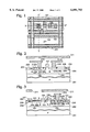
- FIG. 1 is a plan view of one pixel of a solid-state photographic element of a preferred embodiment of the present invention.
- FIG. 2 is a section view taken along line X-X' in FIG. 1.
- FIG. 3 is a section view taken along line Y-Y' in FIG. 1.
- FIG. 4 is a schematic circuit diagram of a preferred embodiment of a solid-state photographic element of the present invention configured in a two-dimensional matrix of pixels.
- FIG. 5 is a pulse timing chart of the operation of the schematic circuit diagram of FIG. 4.
- FIG. 6 is a schematic circuit diagram of a prior art solid-state photographic element.
- FIG. 7 is a pulse timing chart of the operation of the schematic circuit diagram of FIG. 6.
- FIG. 1 is a plan view of one pixel 100 of a solid-state photographic element of the invention.
- FIG. 2 is a section view taken along line X-X' in FIG. 1 and
- FIG. 3 is a section view taken along line Y-Y'.
- the pixel 100 includes a buried photodiode (BPD) 101 that generates and accumulates a charge according to incident light and a junction field effect transistor (JFET) 102 that outputs a signal proportional to the charge, which charge is received at a control region 204 of the JFET.
- BPD buried photodiode
- JFET junction field effect transistor
- a charge storage element 103 is located between the BPD and the JFET and temporarily stores the charge (generated by the BPD 101) before the charge is transferred to the JFET 102.
- a first transfer gate (T GA ) 104 controls the transfer of the charge from the BPD to the charge storage element and a second transfer gate (T GB ) 105 controls transfer of the charge from the charge storage element to the JFET.
- a MOSFET structure having a reset drain (R D ) 106 and a reset gate (R G ) 107 is provided for discharging the charge transmitted to the control region of JFET 102.
- N-type well 202 is installed on p-type silicon substrate 201 (FIGS. 2 and 3).
- BPD 101, JFET 102, and R D 106 are formed by ion injection or thermal diffusion of, for example, boron (B+) or phosphorus (P+), and first transfer gate (T GA ) 104, second transfer gate (T GB ) 105, and reset gate (R G ) 107 are formed by way of an insulating layer (not shown) by a method such as lithography.
- reset gate (R G ) 107 together with p-region 203 of reset drain (R D ) 106 and p-type gate region 204 of JFET 102 form a p-channel MOSFET.
- BPD 101 has an n-type surface layer 205, a p-type accumulation layer 206, an n-type well 202, and a p-type substrate 201, in this sequence from the surface to the reverse side of the semiconductor substrate, thus forming a buried photodiode that has a vertical overflow drain structure.
- JFET 102 is comprised of an n + -type source region 207, an n + -type drain region 208, a p-type gate region (control region) 204, and an n-type channel region 209, and forms a structure in which p-type gate region (control region) 204 is above and below n-type channel 209.
- pattern 211 (preferably an aluminum (Al) film) is attached to reset drain (R D ) 106 to serve as a light-shielding film (light-shielding Al) for shielding all parts of pixel 100 other than BPD 101 (FIGS. 2 and 3).
- Charge storage element 103 is positioned in a p-type diffusion region formed on the surface of n-type well 201 between BPD 101 and JFET 102.
- the charge storage element temporarily stores the charge photoelectrically generated by BPD 101 before the charge is transferred to the control region 203 of JFET 102.
- First transfer gate (T GA ) 104 is formed such that it covers charge storage element 103 and extends from the edge of BPD 101.
- Second transfer gate (T GB ) 105 forms a p-type MOSFET together with the p-type region of charge storage element 103 and the control region 204 of JFET 102.
- These first and second transfer gates 104,105 control charge transfer from the p-type region 206 of BPD 101 to the p-type charge storage element 103, and from the charge storage element 103 to p-type control region 204 of JFET 102.
- the potential of charge storage element 103 drops and the MOSFET that has p-type region 206 as source and p-type charge storage element 103 as drain is switched ON. As a result, the charge potential is transferred from BPD 101 to p-type charge storage element 103.
- first transfer gate 104 and second transfer gate 105 are set to high level, this switches the p-type MOSFETs formed by the two gates OFF. Therefore, the charge transmitted to p-type charge storage element 103 is stored within the charge storage element.
- an inversion layer is formed by applying a voltage of a size that inverts the surface of p-type charge storage element 103 to n-type (4 to 5 V, depending on the diffusion density of p-type charge storage element 103), and the surface state of p-type charge storage element 103 becomes filled with electrons. Therefore, even when a charge is held in p-type charge storage element 103 for a long time deterioration in image quality can be suppressed because there is little dark current.
- first transfer gate 104 is set to high level and second transfer gate 105 is set to low level
- the p-type MOSFET formed by the second transfer gate 105 is switched ON, and the charge in the charge storage element 103 is transferred to the p-type gate 204 (control region) of JFET 102.
- FIG. 4 is a schematic circuit diagram in which the unit pixel 100 shown of FIGS. 1 to 3 is represented as a circuit, along with additional circuitry to provide the pixel signal to output terminals for use in generating a photographic image.
- FIG. 5 is a pulse-timing chart that illustrates the operation of the schematic circuit diagram shown in FIG. 4.
- FIG. 4 represents an array, or matrix, of nine pixels arranged in three rows and three columns. To assist with the following description, a pixel in the third row, third column, is provided with reference numbers. All the pixels are identical.
- a unit pixel 301 includes a photodiode P D that generates and accumulates a charge according to incident light on the pixel.
- a junction field effect transistor JFET receives the charge potential at its control region (gate) and generates an output signal that is proportional to the photodiode charge.
- a charge storage element 1e temporarily stores the charge transferred from the photodiode P D before the charge is transferred to the control region of the JFET.
- a first transfer control element 1a having a first transfer gate T GA , controls transfer of the charge from the photodiode P D to the charge storage element 1e and a second transfer control element 1b, having a second transfer gate T GB , controls transfer of the charge from the charge storage element 1e to the control region of the JFET.
- a reset element 1c includes a reset drain R D for discharging the charge transferred to the control region of the JFET and a reset gate R G that controls switching of the element 1c and hence controls the timing of the discharge via reset drain R D
- each JFET is connected in common to vertical source lines 2a, 2b, and 2c for each column of the matrix layout.
- the drain of each JFET, and the cathode side of each photodiode P D are connected in common for all pixels by a pattern, or diffusion, layer (not shown in the figures), and are connected to power source voltage 1d.
- the anode side of each photodiode P D is connected to the source side of the first transfer control element 1a.
- the control region of each junction field effect transistor JFET is connected to the drain of the second transfer control element 1b.
- First transfer gates T GA are connected in common to respective clock lines 3Aa, 3Ab, and 3Ac that scan under control of a vertical scanning circuit 4 for each row of the matrix layout. Vertical scanning operates in sequence for each row of pixels when drive pulses ⁇ TGA1 , ' TGA2 , and ⁇ TGA3 are provided by the vertical scanning circuit 4.
- the second transfer gates T GB are connected in common to respective clock lines 3Ba, 3Bb, and 3Bc that scan under the control of the vertical scanning circuit 4 for each row of the matrix layout.
- vertical scanning operates in sequence for each row of pixels when drive pulses ⁇ TGB1 , ⁇ TGB2 , and ⁇ TGB3 are provided by the vertical scanning circuit 4.
- Reset element 1c is provided within each pixel 301.
- the reset drains R D are configured parallel to each row of pixels, and are connected in common to respective clock lines 20a, 20b, and 20c that scan under the control of the vertical scanning circuit 4 for each row of the matrix layout.
- the reset gates R G are connected in common for all pixels to drive pulse generating circuit 7 via a line 7a.
- the source of reset element 1c is common with the control region of junction field effect transistor JFET.
- the reset element 1c operates when a drive pulse ⁇ RG is provided from the drive pulse generating circuit 7 and applied to the reset gate R G .
- Each of the vertical source lines 2a, 2b, and 2c are connected to respective electrodes of light signal output accumulating capacitors C S1 , C S2 , and C S3 by way of light signal output transmitting MOS transistors T S1 , T S2 , and T S3 , and to dark signal accumulating capacitors C D1 , C D2 , and C D3 by way of dark output transmitting MOS transistors T D1 , T D2 , and T D3 .
- the accumulating capacitors C S1 , C S2 , C S3 , C D1 , C D2 , and C D3 are connected to signal output line 8 and dark output line 9 through horizontal read select MOS transistors T HS1 , T HS2 , T HS3 , T HD1 , T HD2 , and T HD3 .
- parasitic capacitors C HS and C HD are present on the signal output line 8 and dark output line 9, respectively.
- buffer amplifiers 8a and 9a are connected to signal output line 8 and dark output line 9, respectively.
- the signal output line 8 and dark output line 9 are also connected to the drains of horizontal read reset MOS transistors T HRS and T HRD for resetting the video signal.
- the sources of the horizontal read reset MOS transistors T HRS and T HRD are connected to the light signal output accumulating capacitors C S1 , C S2 , and C S3 and dark signal accumulating capacitors C D1 , C D2 , and C D3 , and then to the ground (GND).
- the horizontal read reset MOS transistors T HRS and T HRD operate when drive pulse ⁇ RH , provided by a drive pulse generating circuit 13, is applied to their gate electrodes.
- Horizontal select signal lines 10a, 10b, and 10c are connected to a horizontal scanning circuit 10 and are connected in common for each column to each of the gate electrodes of the horizontal read select MOS transistors T HS1 , T HS2 , T HS3 , T HD1 , T HD2 , and T HD3 .
- Horizontal reading is controlled by drive pulses ⁇ H1 to ⁇ H3 delivered from the horizontal scanning circuit 10 to the gate electrodes of the horizontal read select MOS transistors.
- the vertical source lines 2a, 2b, and 2c are also connected to the drains of reset transistors T RV1 , T RV2 , and T RV3 and to constant-current sources 14a, 14b, and 14c.
- time interval subscripts indicate the row of pixels and the operation that is being performed.
- the first subscript indicates which row of pixels are undergoing an operation during the time interval and the second subscript indicates the operation.
- the "0" subscript indicates operations performed on all rows of pixels.
- the time intervals t 11 to t 14 correspond as follows: t 11 to the initializing operation of the JFETs, t 12 to the source-follower operation of the first row JFETs after initializing, t 13 to the operation of transferring the signal charges from the first row charge storage elements to the JFETs, and t 14 to the source-follower operation of the JFETs after charge transfer. Furthermore, t 15 is the video signal output interval. The time intervals of t 21 to t 25 and t 31 to t 35 relate to the same operations for the second and third rows, respectively.
- drive pulses ⁇ TGA1 , ⁇ TGA2 , and ⁇ TGA3 are set to a high level (selecting transfer gates T GA OFF) and drive pulses ⁇ TGB1 , ⁇ TGB2 , and ⁇ TGB3 are set to a low level (selecting transfer gates T GB ON) and the signal charges stored in charge storage elements 1e are transferred to the p-type gates of junction field effect transistors JFET, and the charge storage elements 1e are initialized.
- junction field effect transistors JFET Delivering voltage drive pulses ( ⁇ RD1 , ⁇ RD2 , and ⁇ RD3 ) to reset drains R D , junction field effect transistors JFET are selected (ON) or not selected (OFF), and the control regions of junction field effect transistors JFET in selected rows are initialized to the potential at reset drains R D .
- drive pulse ⁇ TGB1 is set to a low level so that the first row transfer gates T GB are changed from non-conducting (OFF) to conducting (ON).
- drive pulse ⁇ TS is set to a high level and drive pulse ⁇ TD is set to a low level so that light signal output transmitting MOS transistors T S1 , T S2 , and T S3 become conducting (ON) and dark output transmitting MOS transistors T D1 , T D2 , and T D3 become non-conducting (OFF).
- drive pulse ⁇ TGB1 is set to a high level so that first row transfer gates T GB become non-conducting (OFF), and drive pulse ⁇ RV is set to a low level so that reset transistors T RV1 to T RV3 are intercepted (OFF).
- each first row JFET performs source-follower operation during time interval t 14 .
- drive pulses ⁇ RD1 , ⁇ RG , and ⁇ TS are set to a low level ( ⁇ TD is held at a low level) and drive pulse ⁇ RV is set to a high level so that output voltages accumulated in light signal output accumulating capacitors C S1 to C S3 and dark signal accumulating capacitors C D1 to C D3 may be output as described below.
- the horizontal read line is reset by setting ⁇ RH to a low value between the sequential drive pulses ⁇ H1 , ⁇ H2 , and ⁇ H3 so that the signal output line 8 and dark output line 9 are temporarily connected to GND through the horizontal reset transistors T RHS and T HRD .
- signals obtained from output terminals V OS and V OD are subjected to computation processing by an external computation circuit not shown in the figure.
- the signal obtained from output terminal V OS contains a light signal component (S) and a dark component (D) and the dark signal obtained from output terminal V OD contains only a dark component (D)
- the signal obtained from output terminal V OS contains a light signal component (S) and a dark component (D)
- the dark signal obtained from output terminal V OD contains only a dark component (D)
- this invention can provide an all-pixel simultaneous electronic shutter.
- photodiodes are reset during the signal charge read interval and the signal output interval, the simultaneous shutter action for all pixels is limited to still pictures.
- the reset operation is performed by discharging the charge accumulated in the photodiode to reset drain R D by way of the JFET control region.
- JFET junction field effect transistor
- MOSFET also can be used as the amplifier.
- a solid-state photographic element was manufactured having a structure as shown in FIGS. 1, 2, and 3 and described above.
- Each pixel of the photographic element includes a buried photodiode (BPD) 101 that generates and accumulates a charge according to incident light, a junction field effect transistor (JFET) 102 that outputs a signal proportionate to the charge received at its control region, a charge storage element 103 that temporarily stores the charge generated and accumulated by the BPD before transmitting it to the JFET, a first transfer gate (T GA ) 104 that controls charge transfer from the BPD to the charge storage element, a second transfer gate (T GB ) 105 that controls charge transfer from the charge storage element 103 to the JFET, a reset drain (R D ) 106 for discharging the charge transferred to the control region of JFET 102, and a reset gate (R G ) 107 that controls the reset drain 106.
- BPD buried photodiode
- JFET junction field effect transistor
- N-type well 202 with an impurity concentration of approximately 3 ⁇ 10 15 cm -3 is installed on p-type silicon substrate 201 with an impurity concentration of approximately 4 ⁇ 10 14 cm -3 .
- BPD 101, JFET 102, and R D 106 are formed by ion injection or thermal diffusion of, for example, boron (B+) or phosphorus (P+), and first transfer gate T GA 104, second transfer gate T GB 105, and reset gate R G 107 are formed by way of an insulating layer (not shown) by a method such as lithography.
- Reset gate R G 107 together with p-region 203 with an impurity concentration of approximately 5 ⁇ 10 18 cm -3 of reset drain R D 106 and p-type gate region 204 of JFET 102 comprise a p-channel MOSFET.
- Photodiode BPD 101 is comprised of a surface n-type layer 205 with an impurity concentration of approximately 2 ⁇ 10 17 cm -3 and p-type charge accumulation layer 206 with an impurity concentration of approximately 3 ⁇ 10 16 cm -3 together with an n-type well and a p-type substrate 201 in this sequence from the surface to the reverse side of the semiconductor substrate, and forms a buried photodiode that has a vertical overflow drain structure.
- JFET 102 is comprised of n+-type source region 207 with an impurity concentration of approximately 2 ⁇ 10 20 cm -3 , n+-type drain region 208 with an impurity concentration of approximately 2 ⁇ 10 20 cm -3 , p-type gate region (control region) 204 with an impurity concentration of approximately 1 ⁇ 10 18 cm -3 , and n-type channel region 209 with an impurity concentration of approximately 1 ⁇ 10 17 cm -3 , and forms a structure in which p-type gate region 204 is on both sides of n-channel 209 above and below.
- reset gate R G 107 By applying a pulse voltage to reset gate R G 107, reset gate R G 107 and reset drain R D 106 initialize control region 204 of JFET 102 to the voltage of reset drain R D 106.
- metal pattern (aluminum (Al) film) 211 is attached to reset drain R D 106 to serve as a light-shielding film (light-shielding Al) for shielding all parts other than buried photodiode BPD 101.
- Charge storage element 103 is positioned in a p-type diffusion region with an impurity concentration of approximately 2 ⁇ 10 16 cm -3 formed on the surface of the n-type well between photodiode BPD 101 and JFET 102, and temporarily stores the charge photoelectrically generated by the photodiode BPD 101 before transferring it to the control region of JFET 102.
- First transfer gate T GA 104 is formed such that it covers charge accumulation layer 103 from the edge of photodiode 101, and second transfer gate T GB 105 forms a p-type MOSFET together with the p-type region of charge accumulation layer 103 and p-type region 204 of the gate of JFET 102.
- These first and second transfer gates 104 and 105 control charge transfer of from p-type region 206 of buried photodiode (BPD) 101 to p-type charge storage element 103, and from charge storage element 103 to p-type gate 204 of JFET 102.
- BPD buried photodiode
Abstract
A solid-state photographic element that can perform electronic shutter action simultaneously for all pixels is disclosed. Each pixel includes a photoelectric converter (such as a photodiode), a first transfer gate, a charge storage element, a second transfer gate, an amplifier, and a reset element. All photodiodes are first reset, then the first transfer gates selected OFF at the same time and charges accumulate in all photodiodes simultaneously. After a predetermined shutter time has elapsed, the first transfer gates are selected ON at the same time and charges that accumulated in the photodiodes are transferred to the corresponding charge storage elements. Thereafter, first transfer gates are selected OFF. A vertical scanning circuit may then select second transfer gates ON sequentially for each row, so that charges accumulated in the charge storage elements are transferred to control regions of corresponding amplifiers. Charges, amplified by the amplifiers, are then stored in light signal output capacitors. Charges stored in light signal output capacitors are read as video signals by column by outputting from a horizontal scanning circuit.
Description
1. Field of the Invention
The present invention pertains to a solid-state photographic element having a plurality of pixels. More particularly, this invention pertains to a solid-state photographic element that can perform electronic shutter action simultaneously for a plurality of pixels.
2. Description of the Related Art
To increase the sensitivity of solid-state photographic elements, a signal amplification, junction field-effect transistor (JFET) may be installed in pixel units in the photographic elements. These are called amplification type solid-state photographic elements. A prior art photographic element includes a photoelectric converter separated from the amplifying transistor and a transfer gate, located between the photoelectric converter and the transistor, that controls transfer of charges (i.e., potential) from the photoelectric converter to the amplifying transistor.
FIG. 6 is a schematic circuit diagram of a prior art amplification type solid-state photographic element. FIG. 7 is a pulse timing chart that illustrates the operation of the schematic circuit diagram shown in FIG. 6.
As shown in FIG. 6, each pixel 31 (only one of nine shown pixels is labeled with reference numbers) is comprised of a transfer control element (a p-channel MOSFET) 31a, a photodiode 1 that generates and accumulates a charge according to incident light, and a JFET 2 that generates a signal output according to the charge received at its control region (the gate). The transfer control element 31a includes a transfer gate electrode TG for controlling transfer of the charge generated and accumulated by photodiode 1 to the control region of JFET 2. A reset element (p-channel MOSFET) 31b having a reset drain RD, is provided for discharging the charge transmitted to the control region of JFET 2. Reset gate RG is a reset control for controlling reset drain RD.
The source of each JFET 2 is connected in common to vertical source lines 32a, 32b, and 32c for each column of the matrix layout. A common drain power source 31c for the all pixels is connected to the drain of each JFET and the cathode side of photodiode 1 by a pattern, or diffusion, layer not represented in the figure. In addition, the control region (gate) of JFET 2 is connected to the drain of transfer control element 31a and the anode side of each photodiode 1 is connected to the source of element 31a.
Transfer gates (transfer gate electrodes) TG of transfer control elements 31a are connected in common to respective clock lines 33a, 33b, and 33c that scan under control of a vertical scanning circuit 34 for each row of the matrix layout. When drive pulses φTG1 to φTG3 are delivered from vertical scanning circuit 34, transfer control elements 31a operate in sequence for each row of pixels.
The reset drains RD of the reset elements 31b are connected in common to clock lines 50a, 50b, and 50c that scan under control of the vertical scanning circuit 34 for each row of the matrix layout. Reset gates (reset gate electrodes) RG are connected in common for all pixels to drive pulse generating circuit 37 by way of row line 37a. In addition, the source of reset element 31b is the same as the drain of transfer control element 31a. Moreover, this is designed such that this reset element 31 b operates when drive pulse φRG delivered from drive pulse generating circuit 37 is applied to the reset gates RG.
Each of vertical source lines 32a, 32b, and 32c is connected to the electrodes of each of light signal output accumulating capacitors (second memory elements) CS1, CS2, and CS3 by way of light signal output transmitting MOS transistors TS1, TS2, and TS3, and to dark signal accumulating capacitors (first memory elements) CD1, CD2, and CD3 by way of dark output transmitting MOS transistors TD1, TD2, and TD3. Respectively, the MOS transistors TS1, TS2, and TS3 and second memory elements CS1, CS2, and CS3, and MOS transistors TD1, TD2, and TD3 and first memory elements CD1, CD2, and CD3 are connected to signal output line 38 and dark output line 39 via horizontal read select MOS transistors THS1, THS2, THS3, THD1, THD2, and THD3. Moreover, generally, parasitic capacitors CHS and CHD are present on signal output line 38 and dark output line 39, respectively. In addition, buffer amplifiers 38a and 39a are connected to signal output line 38 and dark output line 39, respectively.
Horizontal select signal lines 40a, 40b, and 40c are connected to horizontal scanning circuit 40 and are connected in common for each column to each of the gate electrodes of the above-mentioned horizontal read select MOS transistors THS1, THS2, THS3, THD1, THD2, and THD3, and are designed such that horizontal reading is controlled by drive pulses φH1 to φH3 delivered from horizontal scanning circuit 40.
Each of the gate electrodes of the light signal output transmitting MOS transistors TS1, TS2 and TS3 is connected to drive pulse generating circuit 41 by way of light signal clock line 41a, and each of the dark output transmitting MOS transistors TD1, TD2, and TD3 is connected to drive pulse generating circuit 42 by way of dark output clock line 42a. These are designed such that when drive pulse φTS or φTD delivered from drive pulse generating circuits 41 or 42 is applied, light signal output transmitting MOS transistors TS1, TS2, and TS3 or dark output transmitting MOS transistors TD1, TD2, and TD3 operate in a predetermined sequence.
The vertical source lines 32a, 32b, and 32c are connected to the drains of reset transistors TRV1, TRV2, and TRV3 and to source-follower read constant- current sources 44a, 44b, and 44c. In addition, source voltage VRV (e.g., VRV =GND) is supplied to the sources of each reset transistor TRV1, TRV2, and TRV3, and source voltage VCS is supplied to constant- current sources 44a, 44b, and 44c.
Moreover, when reset pulse φRV is supplied to the gate electrodes of reset transistors TRV1, TRV2, and TRV3 and this reset pulse φRV is high level, vertical source lines 32a, 32b, and 32c can be conducted through reset transistors TRV1, TRV2, and TRV3 to ground (VRV =GND).
In addition, constant- current sources 44a, 44b, and 44c are designed such that by suppressing time function discrepancies due to factors such as fluctuation in the bias point for each pixel 31 at the same time that they control the time function of source follower operation, gain is systematized and fixed pattern noise (FPN) is suppressed.
Next, the operation of a photoelectric converter is explained while referring to the pulse timing chart shown in FIG. 7. The operation of reading the first row of pixels 31 is performed in the interval from t11 to t15 (the first digit of the subscript refers to the row undergoing operations). The operations of reading the second row and third rows of pixels are performed during the intervals from t21 to t25 and from t31 to t35, respectively.
In addition, each of t11 to t14 correspond as follows: t11 to the initializing operation of the JFETs 2, t12 to the source-follower operation of JFETs 2 after initializing, t13 to the operation of transmitting a signal charge from first row photodiodes 1 to JFETs 2, and t14 to the source-follower operation of JFETs 2 after transmitting. These four operations are performed during the horizontal blanking interval. Furthermore, t15 is the video signal output interval.
First, as shown in FIG. 7, at the start of interval t11, drive pulse φRD1 is set to high level (with drive pulses φRD2 and φRD3 still at low level), to apply a voltage drive pulse to the reset drains RD of the first row of pixels 31. Because the reset gate RG is ON (i.e., reset element 31b is p-type and φRG is at a low level) and a high level voltage is applied to the reset drains RD, each first row JFET 2 is selected (ON). In addition, because the reset gates RG of all pixels 31 are already conducting (ON), a low-level voltage is transmitted to the control region of the JFETs 2 of the second and third row of pixels 31, the control regions of these JFETs 2 are initialized, and each second and third row JFET 2 is not selected (OFF).
By delivering voltage drive pulses (φRD1, φRD2, and φRD3) to reset drains RD, JFETs 2 are selected (ON) or not selected (OFF), because the control regions of JFET 2 in selected rows are initialized at high-level potential and the control regions of JFET 2 in non-selected rows are initialized at low-level potential.
In addition, at the end of interval t11 (the start of interval t12), by setting drive pulse φRG to high level to make reset gate RG non-conducting (OFF), the control region of each JFET 2 is maintained at their selected (ON) or non-selected (OFF) state.
At the same time (the start of interval t12), by setting drive pulse φRV to low level, reset transistors TRV1 to TRV3 are intercepted (OFF). As a result, each first row JFET 2 performs source-follower operation during this interval t12.
Moreover, during this interval t12, by setting drive pulse φTD to high level, dark output transmitting MOS transistors TD1, TD2, and TD3 become conducting (ON), and output (dark output) voltages corresponding to the potential in the control region of each JFET 2 immediately after initializing are accumulated in dark signal accumulating capacitors CD1, CD2, and CD3.
During interval t13, by setting drive pulse φTG1 to low level, p-type transfer gate TG is changed from non-conducting (OFF) to conducting (ON), and by setting drive pulse φTS to high level and drive pulse φTD to low level, light signal output transmitting MOS transistors TS1, TS2, and TS3 become conducting (ON) and dark output transmitting MOS transistors TD1, TD2, and TD3 become non-conducting (OFF).
As a result, the charges generated and accumulated by the first row photodiodes 1 are transferred to the control regions of JFETs 2. Moreover, the potential in the control region of JFET 2 after this charge is transferred is changed (in this case, increased) by exactly the charge amount divided by gate capacitance. In addition, in FIG. 7, the reason why transfer gate TG becomes conducting (ON) when drive pulse φTG1 is low level is because transfer control element 31a is p-channel type and has the opposite polarity from the other drive pulses.
During interval t14, as in interval t12, by setting drive pulse φTG1 to high level, first row transfer gates TG become non-conducting (OFF) and the charge photoelectrically converted by photodiode 1 is accumulated, and by setting drive pulse φRV to low level, reset transistors TRV1 to TRV3 are intercepted (OFF). As a result, each first row JFET 2 performs source-follower operation.
Moreover, during this interval t14, because drive pulse φTS is high level, light signal output transmitting MOS transistors TS1, TS2, and TS3 become conducting (ON), and output (signal output) voltages corresponding to the potential in the control region of each JFET 2 after charge has been transmitted are accumulated in light signal output accumulating capacitors CS1, CS2, and CS3.
During interval t15, by setting each of drive pulses φRD1, φRG, and φTS to low level and by setting drive pulse φRV to high level, output voltages accumulated in light signal output accumulating capacitors CS1 to CS3 and dark signal accumulating capacitors CD1 to CD3 are prepared for output as described below.
In addition, by outputting drive pulses φH1 to φH3 from horizontal scanning circuit 40 and drive pulse φRH from drive pulse generating circuit 43 in sequence, signals accumulated in light signal output accumulating capacitors CS1 to CS3 and dark signal accumulating capacitors CD1 to CD3 are read by the horizontal read lines of signal output line 38 and dark output line 39, respectively. As signals are output, they are read horizontally by signal output line 38 and dark output line 39, then the horizontal read line is reset.
Moreover, signals obtained from output terminals VOS and VOD are subjected to computation processing by an external computation circuit not shown in the figure. Because the signal obtained from output terminal VOS contains a signal component (S) and a dark component (D) and the signal obtained from output terminal VOD contains only a dark component (D), by subjecting signals obtained from output terminals VOS and VOD to computation processing (subtraction processing (VOS -VOD)), a dark signal corresponding to only the signal component (S) is extracted.
First row reading operating corresponding to interval t11 to t15 described above is repeated in the same way for the second and third rows during the interval from t21 to t25 and the interval from t31 to t35.
However, a solid-state photographic element such as shown in FIG. 6 can not perform electronic shutter action simultaneously for all pixels. To perform electronic shutter action simultaneously for all pixels, photoelectric converters must be reset simultaneously for all pixels and signal charges accumulated by photoelectric converters simultaneously for all pixels must be transmitted to amplifiers simultaneously for all pixels.
However, in prior art solid-state photographic elements, a charge accumulated by a photoelectric converter (buried photodiode) is transmitted to an amplifier (JFET 2) for each row sequentially and cannot be transmitted simultaneously in all pixels. If prior art elements where set to transfer the charge simultaneously in all pixels no video signal would result because the amplifiers (JFET 2) of all pixels would be ON simultaneously and signals to light signal accumulating capacitors or dark output accumulating capacitors would be accumulated simultaneously for all pixels. To provide a video signal it is necessary to read the charges sequentially.
The present invention provides an amplification type solid-state photographic element that can perform electronic shutter operation simultaneously for all pixels, reduce dark current and latent images, and be assembled in a large scale integrated circuit (LSI), to obtain an LSI that has high source-follower operation gain, and to greatly reduce dark current caused by surface states.
The present invention locates within a pixel a charge storage element between a photoelectric converter and an amplifier that temporarily stores charges from the photoelectric converter. A first transfer gate is located between the photoelectric converter and the charge storage element and a second transfer gate is located between the amplifier and the charge storage element to control the transfer of charges from the photoelectric converter to the charge storage element and to the amplifier.
Thus, a solid-state photographic element of the present invention provides a unit pixel having a photoelectric converter that generates and accumulates a charge according to incident light. An amplifier is provided that generates an output signal according to a charge potential received from the photoelectric converter at a control region of the amplifier. The charge storage element is located between the amplifier and the photoelectric converter to temporary store the charge. A first transfer gate controls transfer of the charge from the photoelectric converter to the charge storage element and a second transfer gate controls transfer of the charge from the charge storage element to the control region of the amplifier. A reset element is provided to discharge the charge at the amplifier control region.
When a junction field effect transistor (JFET) is used as the amplifier, for example, the reset element may be a switching means for discharging the charge in the control region. If the amplifier is a MOSFET, the reset element may be a means that discharges the charge of the control region by directly controlling the control region.
In operation, the first transfer gates may be switched ON at the same time for all pixels and charges are transferred from the photoelectric converters to the charge storage elements simultaneously. The photoelectric converters are thus initialized simultaneously for all pixels. Charges transmitted to the charge storage elements are then transferred to the control region of the amplifiers by way of the second transfer gates, then further discharged to reset lines by the reset elements.
By switching first transfer gates ON, then OFF, at the same time for all pixels, charges start to accumulate in the photoelectric converters at the same time. The interval in which the first transfer gates are switched OFF corresponds to the exposure time. When first transfer gates are switched ON again at the same time, charges accumulated in the photoelectric converters during the exposure time are transferred to the charge storage elements at the same time. Then, by switching the first transfer gates OFF at the same time, the charges accumulated in the charge storage elements remain in the charge storage elements.
Thereafter, the second transfer gates are switched ON in sequence so that charges accumulated in the charge storage elements are delivered to the control region of the amplifiers in sequence in the same way as in the solid-state photographic element shown in FIG. 6. The subsequent operations of the solid-state photographic element are substantially the same as the operation of the solid-state photographic element shown in FIG. 6.
In preferred embodiments, the photoelectric converter is a buried photodiode having a buried region of a first conductive type that is buried in a semiconductor substrate of a second conductive type and a depletion prevention region that contacts the surface of the semiconductor substrate and is installed between the surface of the semiconductor substrate and the above-mentioned buried region. This embodiment of the photoelectric converter can reduce dark current and image lag.
Preferably, the second transfer gate is a MOS gate located between the amplifier and the charge storage element and the charge storage element is a diffusion region of the first conductive type on the surface of the semiconductor substrate between the second transfer gate and the photoelectric converter. The first transfer gate is a MOS gate located between the second transfer gate and the photoelectric converter, and covers the charge storage element. This embodiment further assists fabricating the solid-state photographic elements in an LSI, enabling high integration of solid-state photographic elements.
Preferably, the amplifier is a junction field effect transistor (JFET). permitting high source-follower operation gain. In addition, because signal charges in JFET control regions are not dissipated during the amplification operation such as in a bipolar transistor, noise can be reduced.
Preferably, when the first transfer gate (MOS gate) is OFF a switching voltage is of a level that forms an inversion layer on the surface of the charge storage element. According to this means, by filling the surface state of the charge storage element with electrons, this greatly reduces dark current caused by surface state.
FIG. 1 is a plan view of one pixel of a solid-state photographic element of a preferred embodiment of the present invention.
FIG. 2 is a section view taken along line X-X' in FIG. 1.
FIG. 3 is a section view taken along line Y-Y' in FIG. 1.
FIG. 4 is a schematic circuit diagram of a preferred embodiment of a solid-state photographic element of the present invention configured in a two-dimensional matrix of pixels.
FIG. 5 is a pulse timing chart of the operation of the schematic circuit diagram of FIG. 4.
FIG. 6 is a schematic circuit diagram of a prior art solid-state photographic element.
FIG. 7 is a pulse timing chart of the operation of the schematic circuit diagram of FIG. 6.
Preferred embodiments of the present invention are described below with reference to FIGS. 1-5. FIG. 1 is a plan view of one pixel 100 of a solid-state photographic element of the invention. FIG. 2 is a section view taken along line X-X' in FIG. 1 and FIG. 3 is a section view taken along line Y-Y'. The pixel 100 includes a buried photodiode (BPD) 101 that generates and accumulates a charge according to incident light and a junction field effect transistor (JFET) 102 that outputs a signal proportional to the charge, which charge is received at a control region 204 of the JFET. A charge storage element 103 is located between the BPD and the JFET and temporarily stores the charge (generated by the BPD 101) before the charge is transferred to the JFET 102. A first transfer gate (TGA) 104 controls the transfer of the charge from the BPD to the charge storage element and a second transfer gate (TGB) 105 controls transfer of the charge from the charge storage element to the JFET. A MOSFET structure having a reset drain (RD) 106 and a reset gate (RG) 107 is provided for discharging the charge transmitted to the control region of JFET 102.
N-type well 202 is installed on p-type silicon substrate 201 (FIGS. 2 and 3). In this well, BPD 101, JFET 102, and R D 106 are formed by ion injection or thermal diffusion of, for example, boron (B+) or phosphorus (P+), and first transfer gate (TGA) 104, second transfer gate (TGB) 105, and reset gate (RG) 107 are formed by way of an insulating layer (not shown) by a method such as lithography.
As shown in FIG. 2, reset gate (RG) 107 together with p-region 203 of reset drain (RD) 106 and p-type gate region 204 of JFET 102 form a p-channel MOSFET.
In addition, as shown in FIG. 3, BPD 101 has an n-type surface layer 205, a p-type accumulation layer 206, an n-type well 202, and a p-type substrate 201, in this sequence from the surface to the reverse side of the semiconductor substrate, thus forming a buried photodiode that has a vertical overflow drain structure.
Moreover, although not shown in FIG. 1 (to avoid covering the components discussed), pattern 211 (preferably an aluminum (Al) film) is attached to reset drain (RD) 106 to serve as a light-shielding film (light-shielding Al) for shielding all parts of pixel 100 other than BPD 101 (FIGS. 2 and 3).
First transfer gate (TGA) 104 is formed such that it covers charge storage element 103 and extends from the edge of BPD 101. Second transfer gate (TGB) 105 forms a p-type MOSFET together with the p-type region of charge storage element 103 and the control region 204 of JFET 102. These first and second transfer gates 104,105 control charge transfer from the p-type region 206 of BPD 101 to the p-type charge storage element 103, and from the charge storage element 103 to p-type control region 204 of JFET 102.
Thus, when the first transfer gate 104 is set to low level (transfer gate 104 ON) and the second transfer gate 105 is set to high level (transfer gate 105 OFF), the potential of charge storage element 103 drops and the MOSFET that has p-type region 206 as source and p-type charge storage element 103 as drain is switched ON. As a result, the charge potential is transferred from BPD 101 to p-type charge storage element 103.
Next, when both first transfer gate 104 and second transfer gate 105 are set to high level, this switches the p-type MOSFETs formed by the two gates OFF. Therefore, the charge transmitted to p-type charge storage element 103 is stored within the charge storage element. At this time, an inversion layer is formed by applying a voltage of a size that inverts the surface of p-type charge storage element 103 to n-type (4 to 5 V, depending on the diffusion density of p-type charge storage element 103), and the surface state of p-type charge storage element 103 becomes filled with electrons. Therefore, even when a charge is held in p-type charge storage element 103 for a long time deterioration in image quality can be suppressed because there is little dark current.
Next, when first transfer gate 104 is set to high level and second transfer gate 105 is set to low level, the p-type MOSFET formed by the second transfer gate 105 is switched ON, and the charge in the charge storage element 103 is transferred to the p-type gate 204 (control region) of JFET 102.
FIG. 4 is a schematic circuit diagram in which the unit pixel 100 shown of FIGS. 1 to 3 is represented as a circuit, along with additional circuitry to provide the pixel signal to output terminals for use in generating a photographic image. FIG. 5 is a pulse-timing chart that illustrates the operation of the schematic circuit diagram shown in FIG. 4.
The schematic of FIG. 4 represents an array, or matrix, of nine pixels arranged in three rows and three columns. To assist with the following description, a pixel in the third row, third column, is provided with reference numbers. All the pixels are identical.
A unit pixel 301 includes a photodiode PD that generates and accumulates a charge according to incident light on the pixel. A junction field effect transistor JFET receives the charge potential at its control region (gate) and generates an output signal that is proportional to the photodiode charge. A charge storage element 1e temporarily stores the charge transferred from the photodiode PD before the charge is transferred to the control region of the JFET. A first transfer control element 1a, having a first transfer gate TGA, controls transfer of the charge from the photodiode PD to the charge storage element 1e and a second transfer control element 1b, having a second transfer gate TGB, controls transfer of the charge from the charge storage element 1e to the control region of the JFET. A reset element 1c includes a reset drain RD for discharging the charge transferred to the control region of the JFET and a reset gate RG that controls switching of the element 1c and hence controls the timing of the discharge via reset drain RD.
The source of each JFET is connected in common to vertical source lines 2a, 2b, and 2c for each column of the matrix layout. In addition, the drain of each JFET, and the cathode side of each photodiode PD, are connected in common for all pixels by a pattern, or diffusion, layer (not shown in the figures), and are connected to power source voltage 1d. Furthermore, the anode side of each photodiode PD is connected to the source side of the first transfer control element 1a. The control region of each junction field effect transistor JFET is connected to the drain of the second transfer control element 1b.
First transfer gates TGA are connected in common to respective clock lines 3Aa, 3Ab, and 3Ac that scan under control of a vertical scanning circuit 4 for each row of the matrix layout. Vertical scanning operates in sequence for each row of pixels when drive pulses φTGA1, 'TGA2, and φTGA3 are provided by the vertical scanning circuit 4.
Likewise, the second transfer gates TGB are connected in common to respective clock lines 3Ba, 3Bb, and 3Bc that scan under the control of the vertical scanning circuit 4 for each row of the matrix layout. Again, vertical scanning operates in sequence for each row of pixels when drive pulses φTGB1, φTGB2, and φTGB3 are provided by the vertical scanning circuit 4.
Each of the vertical source lines 2a, 2b, and 2c are connected to respective electrodes of light signal output accumulating capacitors CS1, CS2, and CS3 by way of light signal output transmitting MOS transistors TS1, TS2, and TS3, and to dark signal accumulating capacitors CD1, CD2, and CD3 by way of dark output transmitting MOS transistors TD1, TD2, and TD3. The accumulating capacitors CS1, CS2, CS3, CD1, CD2, and CD3 are connected to signal output line 8 and dark output line 9 through horizontal read select MOS transistors THS1, THS2, THS3, THD1, THD2, and THD3. Moreover, parasitic capacitors CHS and CHD are present on the signal output line 8 and dark output line 9, respectively. In addition, buffer amplifiers 8a and 9a are connected to signal output line 8 and dark output line 9, respectively.
The signal output line 8 and dark output line 9 are also connected to the drains of horizontal read reset MOS transistors THRS and THRD for resetting the video signal. The sources of the horizontal read reset MOS transistors THRS and THRD are connected to the light signal output accumulating capacitors CS1, CS2, and CS3 and dark signal accumulating capacitors CD1, CD2, and CD3, and then to the ground (GND). In addition, the horizontal read reset MOS transistors THRS and THRD operate when drive pulse φRH, provided by a drive pulse generating circuit 13, is applied to their gate electrodes.
Horizontal select signal lines 10a, 10b, and 10c are connected to a horizontal scanning circuit 10 and are connected in common for each column to each of the gate electrodes of the horizontal read select MOS transistors THS1, THS2, THS3, THD1, THD2, and THD3. Horizontal reading is controlled by drive pulses φH1 to φH3 delivered from the horizontal scanning circuit 10 to the gate electrodes of the horizontal read select MOS transistors.
Each of the gate electrodes of the light signal output transmitting MOS transistors TS1, TS2, and TS3 is connected to drive pulse generating circuit 11 by way of light signal clock line 11a. Each of the dark output transmitting MOS transistors TD1, TD2, and TD3 is connected to drive pulse generating circuit 12 by way of dark output clock line 12a. When drive pulses φTS or φTD, provided from the drive pulse generating circuits 11 or 12, are applied to the respective gate electrodes, the light signal output transmitting MOS transistors TS1, TS2, and TS3 or dark output transmitting MOS transistors TD1, TD2, and TD3 operate alternately in a predetermined sequence.
The vertical source lines 2a, 2b, and 2c are also connected to the drains of reset transistors TRV1, TRV2, and TRV3 and to constant- current sources 14a, 14b, and 14c.
Moreover, when a vertical reset pulse φRV is supplied to the gate electrodes of reset transistors TRV1, TRV2, and TRV3 and this reset pulse φRV is high level, the vertical source lines 2a, 2b, and 2c can be conducted through reset transistors TRV1, TRV2, and TRV3 to ground (VRV =GND). In addition, constant- current sources 14a, 14b, and 14c are designed such that by suppressing time function discrepancies due to factors such as fluctuation in the bias point for each pixel 301 at the same time that they control the time function of source follower operation, gain is systematized and fixed pattern noise (FPN) is suppressed.
Next, the operation of a solid-state photographic element according to this invention is explained while referring to the pulse timing chart shown in FIG. 5. The operation of resetting the photodiode and accumulating a signal charge in the photodiode and the operation of transferring the charge from the photodiode to the charge storage element occur during the interval from t01 to t04. Reading the first row of pixels 301 is performed during the interval from t11 to t15. And, reading the second row and third row of pixels is performed during the intervals from t21 to t25 and from t31 to t35, respectively.
Note that the time interval subscripts indicate the row of pixels and the operation that is being performed. The first subscript indicates which row of pixels are undergoing an operation during the time interval and the second subscript indicates the operation. The "0" subscript indicates operations performed on all rows of pixels.
The time intervals t11 to t14 correspond as follows: t11 to the initializing operation of the JFETs, t12 to the source-follower operation of the first row JFETs after initializing, t13 to the operation of transferring the signal charges from the first row charge storage elements to the JFETs, and t14 to the source-follower operation of the JFETs after charge transfer. Furthermore, t15 is the video signal output interval. The time intervals of t21 to t25 and t31 to t35 relate to the same operations for the second and third rows, respectively.
First, as shown in FIG. 5, during time interval t01, drive pulses φTGA1, φTGA2, and φTGA3 are set to a low level thereby selecting ON the p-type transfer gates TGA so that the signal charges accumulated in photodiodes PD are transferred to charge storage elements 1e. Thus, all photodiodes PD are initialized simultaneously for all pixels (all rows, all columns). Next, during interval t02, drive pulses φTGA1, φTGA2, and φTGA3 are set to a high level (selecting transfer gates TGA OFF) and drive pulses φTGB1, φTGB2, and φTGB3 are set to a low level (selecting transfer gates TGB ON) and the signal charges stored in charge storage elements 1e are transferred to the p-type gates of junction field effect transistors JFET, and the charge storage elements 1e are initialized.
At this time, drive pulse φRG is at a low level and applied to reset gates RG. Because reset element 1c is a p-type MOSFET, it is switched ON. Therefore, the signal charges transmitted to the p-type gate of junction field effect transistor JFET are discharged through reset drain RD.
In addition, when drive pulses φTGA1, φTGA2, and φTGA3 are high level during time interval t02, photodiodes PD simultaneously start to accumulate charges generated by photoelectric conversion.
Therefore, beginning at the start of interval t02, (the end of interval t01) when φTGA1, φTGA2, and φTGA3 are at a high level and ending when φTGA1, φTGA2, and φTGA3 are made low level at the end of interval t03 (the start of interval t04) is the charge accumulation time of photodiode PD. Thus, charge accumulation time (shutter speed) can be set to the desired time by controlling the length of interval t03. Next, during interval t04, pulses φTGA1, φTGA2, and φTGA3 are set to a low level and the signal charges accumulated in the photodiodes are transferred to the charge storage elements simultaneously for all pixels.
At the start of interval t11, drive pulse φRD1 is set to a high level (with drive pulses φRD2 and φRD3 maintained at a low level), and is applied to the reset drains RD of the first row of pixels. This operation causes the voltage to be transferred to the control region of each of the junction field effect transistors JFET of the first row of pixels and the junction field effect transistors JFET are selected (ON). The reset gates RG of all pixels are already ON because φRG is at a low level and reset elements 1e are p-type. Each second and subsequent row junction field effect transistor JFET is not selected (OFF) because φRD2 and φRD3 are maintained at a low level.
Delivering voltage drive pulses (φRD1, φRD2, and φRD3) to reset drains RD, junction field effect transistors JFET are selected (ON) or not selected (OFF), and the control regions of junction field effect transistors JFET in selected rows are initialized to the potential at reset drains RD.
In addition, at the end of interval tag (the start of interval t12), drive pulse φRG is set to a high level to make all reset gates RG non-conducting (OFF) and the control regions of each junction field effect transistor JFET are maintained at their respective selected (ON), or non-selected (OFF), states.
At the same time (the start of interval t12), by setting drive pulse φRV to low level, reset transistors TRV1 to TRV3 are intercepted (OFF). As a result, each first row junction field effect transistor JFET performs source-follower operation during this interval t12. Moreover, during this interval t12, by setting drive pulse φTD to high level, dark output transmitting MOS transistors TD1, TD2, and TD3 become conducting (ON), and output (dark output) voltages corresponding to the potential in the control region of each JFET immediately after initializing are accumulated in dark signal accumulating capacitors CD1, CD2, and CD3.
During interval t13, drive pulse φTGB1 is set to a low level so that the first row transfer gates TGB are changed from non-conducting (OFF) to conducting (ON). Also, drive pulse φTS is set to a high level and drive pulse φTD is set to a low level so that light signal output transmitting MOS transistors TS1, TS2, and TS3 become conducting (ON) and dark output transmitting MOS transistors TD1, TD2, and TD3 become non-conducting (OFF).
As a result, the charges generated by first row photodiodes PD and stored in charge storage elements 1e are transferred to the control regions of junction field effect transistors JFET. Moreover, the potential in the control region of junction field effect transistor JFET after this charge is transferred is changed (in this case, increased) proportionately to the charge amount divided by gate capacitance. In addition, in FIG. 4, the reason why transfer gate TGB becomes conducting (ON) when drive pulse φTGB1 is low level is because transfer control element 1a is p-channel type and has the opposite polarity from the other drive pulses.
During interval t14, drive pulse φTGB1 is set to a high level so that first row transfer gates TGB become non-conducting (OFF), and drive pulse φRV is set to a low level so that reset transistors TRV1 to TRV3 are intercepted (OFF). As a result, each first row JFET performs source-follower operation during time interval t14.
Moreover, during time interval t14, because drive pulse φTS is at a high level, light signal output transmitting MOS transistors TS1, TS2, and TS3 are conducting (ON), and light signal output voltages (corresponding to the potential in the control region of each first row junction field effect transistor JFET) are accumulated in light signal output accumulating capacitors CS1, CS2, and CS3.
During interval t15, drive pulses φRD1, φRG, and φTS are set to a low level (φTD is held at a low level) and drive pulse φRV is set to a high level so that output voltages accumulated in light signal output accumulating capacitors CS1 to CS3 and dark signal accumulating capacitors CD1 to CD3 may be output as described below.
By outputting drive pulse φRH from drive pulse generating circuit 13 and drive pulses φH1 to φH3 from horizontal scanning circuit 10 in sequence, signals accumulated in light signal output accumulating capacitors CS1 to CS3 and dark signal accumulating capacitors CD1 to CD3 are read by the horizontal read lines of signal output line 8 and dark output line 9, respectively, and output to terminals VOS and VOD. After each signal from each column is output from output terminals VOS and VOD, the horizontal read line is reset by setting φRH to a low value between the sequential drive pulses φH1, φH2, and φH3 so that the signal output line 8 and dark output line 9 are temporarily connected to GND through the horizontal reset transistors TRHS and THRD. Moreover, signals obtained from output terminals VOS and VOD are subjected to computation processing by an external computation circuit not shown in the figure. Because the signal obtained from output terminal VOS contains a light signal component (S) and a dark component (D) and the dark signal obtained from output terminal VOD contains only a dark component (D), by subjecting signals obtained from output terminals VOS and VOD to computation processing (subtraction processing (VOS -VOD)), a signal corresponding to only the light signal component (S) is extracted.
As described above, this invention can provide an all-pixel simultaneous electronic shutter. However, in the present embodiment, because photodiodes are reset during the signal charge read interval and the signal output interval, the simultaneous shutter action for all pixels is limited to still pictures.
In the example explained above, the reset operation is performed by discharging the charge accumulated in the photodiode to reset drain RD by way of the JFET control region. However, it also is possible to reset photodiodes by discharging the photodiode charge from the charge accumulation layer of the photodiode to the substrate by controlling the potential applied to the substrate. In this case, because photodiodes are reset regardless of the relationship between the charge reading part and the dark output part, it possible to achieve an all-pixel simultaneous electronic shutter for moving pictures.
Moreover, in the preferred embodiment described above, a junction field effect transistor JFET was used as the amplifier. However, a MOSFET also can be used as the amplifier.
A solid-state photographic element was manufactured having a structure as shown in FIGS. 1, 2, and 3 and described above.
Each pixel of the photographic element includes a buried photodiode (BPD) 101 that generates and accumulates a charge according to incident light, a junction field effect transistor (JFET) 102 that outputs a signal proportionate to the charge received at its control region, a charge storage element 103 that temporarily stores the charge generated and accumulated by the BPD before transmitting it to the JFET, a first transfer gate (TGA) 104 that controls charge transfer from the BPD to the charge storage element, a second transfer gate (TGB) 105 that controls charge transfer from the charge storage element 103 to the JFET, a reset drain (RD) 106 for discharging the charge transferred to the control region of JFET 102, and a reset gate (RG) 107 that controls the reset drain 106.
N-type well 202 with an impurity concentration of approximately 3×1015 cm-3 is installed on p-type silicon substrate 201 with an impurity concentration of approximately 4×1014 cm-3. In this well 202, BPD 101, JFET 102, and R D 106 are formed by ion injection or thermal diffusion of, for example, boron (B+) or phosphorus (P+), and first transfer gate T GA 104, second transfer gate T GB 105, and reset gate R G 107 are formed by way of an insulating layer (not shown) by a method such as lithography.
By applying a pulse voltage to reset gate R G 107, reset gate R G 107 and reset drain R D 106 initialize control region 204 of JFET 102 to the voltage of reset drain R D 106.
Moreover, although not shown in FIG. 1, as can be understood from FIGS. 2 and 3, metal pattern (aluminum (Al) film) 211 is attached to reset drain R D 106 to serve as a light-shielding film (light-shielding Al) for shielding all parts other than buried photodiode BPD 101.
First transfer gate T GA 104 is formed such that it covers charge accumulation layer 103 from the edge of photodiode 101, and second transfer gate T GB 105 forms a p-type MOSFET together with the p-type region of charge accumulation layer 103 and p-type region 204 of the gate of JFET 102. These first and second transfer gates 104 and 105 control charge transfer of from p-type region 206 of buried photodiode (BPD) 101 to p-type charge storage element 103, and from charge storage element 103 to p-type gate 204 of JFET 102.
This specification sets forth the best mode for carrying out the invention as known at the time of filing the patent application and provides sufficient information to enable a person skilled in the art to make and use the invention. The specification further describes materials, shapes, configurations and arrangements of parts for making a using the invention. However, it is intended that the scope of the invention shall be limited by the language of the claims and the law of the land as pertains to valid U.S. patents.
Claims (24)
1. A solid-state photographic element having a plurality of pixels, each pixel including a photoelectric converter that generates and accumulates a charge potential according to incident light, an amplifier having a control region in communication with the photoelectric converter wherein the amplifier generates a signal output in response to the charge potential from the photoelectric converter, and a reset element for discharging the charge potential received at the control region of the amplifier, the improvement comprising:
(a) a charge storage element located between the amplifier and the photoelectric converter that stores the charge potential;
(b) a first transfer gate that controls a transfer of the charge potential from the photoelectric converter to the charge storage element; and
(c) a second transfer gate that controls a transfer of the charge potential from the charge storage element to the control region of the amplifier.
2. The solid-state photographic element of claim 1 wherein the photoelectric converter is a buried photodiode comprising a buried region of a first conductive type buried in a semiconductor substrate of a second conductive type and a depletion prevention region of the second conductive type that contacts a surface of the semiconductor substrate and is located between the surface of the semiconductor substrate and the buried region.
3. The solid-state photographic element of claim 2 wherein the second transfer gate is comprised of a metal oxide semiconductor gate located between the amplifier and the charge storage element, and the charge storage element is comprised of a diffusion region of a first conductive type proximate a surface of a semiconductor substrate and is located between the second transfer gate and the photoelectric converter, and the first transfer gate is comprised of a metal oxide semiconductor gate located between the second transfer gate and the photoelectric converter and substantially covers the charge storage element.
4. The solid-state photographic element of claim 1 wherein the amplifier is a junction field effect transistor.
5. The solid-state photographic element of claim 3 wherein the first transfer gate includes a voltage that selects the first transfer gate OFF and the voltage forms an inversion layer on a surface of the charge storage element.
6. A solid-state photographic element having a plurality of pixels and wherein each pixel comprises:
(a) a photoelectric converter;
(b) a first transfer gate in communication with the photoelectric converter;
(c) a charge storage element in communication with the first transfer gate and when the first transfer gate is selected ON, the charge storage element is in communication with the photoelectric converter;
(d) a second transfer gate in communication with the charge storage element; and
(e) an amplifier in communication with the second transfer gate and a power source and when the second transfer gate is selected ON the amplifier is in communication with the charge storage element;
(f) wherein incident light generates a plurality of electric potentials in a respective plurality of photoelectric converters of a plurality of pixels and the electric potentials can be simultaneously transferred from the plurality of photoelectric converters to a respective plurality of charge storage elements when the respective plurality of first transfer gates are selected ON and the plurality of electric potentials can be sequentially transferred from the plurality of charge storage elements to a respective plurality of amplifiers when the second transfer gates are sequentially selected ON and the plurality of amplifiers provide a respective plurality of signals corresponding to the plurality of electric potentials generated by the plurality of photoelectric converters.
7. The solid-state photographic element of claim 6 wherein the photoelectric converter is a photodiode.
8. The solid-state photographic element of claim 6 wherein the amplifier is a junction field effect transistor.
9. The solid-state photographic element of claim 6 wherein the solid-state photographic element is fabricated on a semiconductor substrate of a first conductive type having a well of a second conductive type formed therein.
10. The solid-state photographic element of claim 9 wherein the photoelectric converter is a buried photodiode comprising a buried region of the first conductive type buried in the well and a depletion prevention region of the second conductive type that contacts a surface of the semiconductor substrate and is located between the surface of the semiconductor substrate and the buried region.
11. The solid-state photographic element of claim 9 wherein the amplifier is a junction field effect transistor comprising a source region of the second conductive type formed in the well of the semiconductor substrate and a drain region of the second conductive type formed in the well of the semiconductor substrate and a gate region of the first conductive type formed in the well of the semiconductor substrate.
12. The solid-state photographic element of claim 11 wherein the amplifier further comprises a channel region of the second conductive type and the gate region of the first conductive type is formed above and below the channel region of the second conductive type.
13. The solid-state photographic element of claim 9 wherein the charge storage element comprises a storage region of the first conductive type in the well of the semiconductor substrate and the charge storage element is located between the photoelectric converter and the amplifier.
14. The solid-state photographic element of claim 9 wherein the photoelectric converter is a buried photodiode comprising a buried region of a first conductive type buried in the well and a depletion prevention region of the second conductive type that contacts a surface of the semiconductor substrate and is located between the surface of the semiconductor substrate and the buried region and wherein the amplifier is a junction field effect transistor comprising a source region of the second conductive type formed in the well of the semiconductor substrate and a drain region of the second conductive type formed in the well of the semiconductor substrate and a gate region of the first conductive type formed in the well of the semiconductor substrate and wherein the charge storage element comprises a storage region of the first conductive type in the well of the semiconductor substrate and the charge storage element is located between the photoelectric converter and the amplifier.
15. The solid-state photographic element of claim 14 wherein the first transfer gate comprises a gate overlaying the charge storage element and extending toward the photoelectric converter such that the first transfer gate together with the buried region of the photoelectric converter and the storage region of the charge storage element form a metal oxide semiconductor transistor.
16. The solid-state photographic element of claim 14 wherein the second transfer gate comprises a gate located proximate the charge storage element and the amplifier such that the gate together with the storage region of the charge storage element and the gate region of the amplifier form a metal oxide semiconductor transistor.
17. The solid-state photographic element of claim 9 further comprising a reset element comprising a gate located proximate the amplifier and a drain region of the first conductive type and the reset element gate together with the reset element drain region and the gate region of the amplifier form metal oxide semiconductor field effect transistor.
18. A method of shuttering a plurality of pixels of a solid-state photographic element, the pixels each having a photoelectric converter, a charge storage element, a first transfer gate, a second transfer gate and an amplifier, comprising the steps of:
(a) exposing a plurality of photoelectric converters to incident light and generating a respective plurality of charge potentials;
(a) transferring the plurality of charge potentials from the plurality of photoelectric converters to a respective plurality of charge storage elements simultaneously; and
(b) transferring the plurality of charge potentials from the plurality of charge storage elements to a respective plurality of amplifiers sequentially to provide a video signal.
19. The method of claim 18 wherein the step of transferring the plurality of charge potentials from the plurality of photoelectric converters to a respective plurality of charge storage elements simultaneously includes selecting ON the plurality of first transfer gates and selecting OFF the plurality of second transfer gates.
20. The method of claim 18 wherein the step transferring the plurality of charge potentials from the plurality of charge storage elements to a respective plurality of amplifiers sequentially includes selecting OFF the plurality of first transfer gates and selecting ON the plurality of second transfer gates in a predetermined sequence.
21. The method of claim 18 further comprising the steps of initializing the plurality of photoelectric converters simultaneously before exposing the plurality of photoelectric converters to incident light.
22. The method of claim 21 wherein the step of initializing the plurality of photoelectric converters comprises simultaneously selecting ON the plurality of first transfer gates during a first time period and then simultaneously selecting OFF the plurality of first transfer gates and selecting ON the plurality of second transfer gates during a second time period and wherein the pixels each include a reset element that is selected ON during the second time period.
23. The method of claim 21 wherein the step on initializing the plurality of photoelectric converters comprises applying a voltage potential to a substrate wherein the photoelectric converter is formed.
24. The method of claim 18 further comprising the steps of initializing the plurality of photoelectric converters prior to exposing the plurality of photoelectric converters to incident for an exposure time period.
Applications Claiming Priority (2)
| Application Number | Priority Date | Filing Date | Title |
|---|---|---|---|
| JP9-350163 | 1997-12-05 | ||
| JP35016397A JP3874135B2 (en) | 1997-12-05 | 1997-12-05 | Solid-state image sensor |
Publications (1)
| Publication Number | Publication Date |
|---|---|
| US6091793A true US6091793A (en) | 2000-07-18 |
Family
ID=18408663
Family Applications (1)
| Application Number | Title | Priority Date | Filing Date |
|---|---|---|---|
| US09/204,625 Expired - Lifetime US6091793A (en) | 1997-12-05 | 1998-12-01 | Solid-state photographic device having a charge storage element for simultaneous shutter action |
Country Status (2)
| Country | Link |
|---|---|
| US (1) | US6091793A (en) |
| JP (1) | JP3874135B2 (en) |
Cited By (24)
| Publication number | Priority date | Publication date | Assignee | Title |
|---|---|---|---|---|
| US6590611B1 (en) | 1997-11-28 | 2003-07-08 | Nikon Corporation | Solid-state image-pickup devices and methods for motion detection |
| US20030164887A1 (en) * | 2002-02-27 | 2003-09-04 | Canon Kabushiki Kaisha | Signal processing device and image pickup apparatus using the same |
| US20050040393A1 (en) * | 2003-08-22 | 2005-02-24 | Hong Sungkwon C. | Imaging with gate controlled charge storage |
| US20050121519A1 (en) * | 2003-12-05 | 2005-06-09 | Canon Kabushiki Kaisha | Solid state image pickup device, method of driving solid state image pickup device, and camera using the solid state image pickup device |
| US20050162537A1 (en) * | 2003-12-25 | 2005-07-28 | Yoshitaka Egawa | Solid-state imaging device, digital camera, and digital video camera |
| US20060028568A1 (en) * | 2004-08-06 | 2006-02-09 | Nobuhiro Takeda | Image capturing apparatus |
| US20060219868A1 (en) * | 2005-03-29 | 2006-10-05 | Konica Minolta Holdings, Inc. | Solid-state image-sensing device |
| US20090032853A1 (en) * | 2007-07-30 | 2009-02-05 | Samsung Electronics Co., Ltd. | CMOS image sensors and methods of fabricating the same |
| US20090050993A1 (en) * | 2007-08-24 | 2009-02-26 | Canon Kabushiki Kaisha | Photoelectric conversion device and multi-chip image sensor |
| US20090086063A1 (en) * | 2006-06-03 | 2009-04-02 | Nikon Corporation | Solid-state imaging device and imaging apparatus using the same |
| US20090290059A1 (en) * | 2007-02-06 | 2009-11-26 | Nikon Corporation | Connection/separation element in photoelectric converter portion, solid-state imaging device, and imaging apparatus |
| US20100091161A1 (en) * | 2007-06-16 | 2010-04-15 | Nikon Corporation | Solid-state image sensor and imaging apparatus equipped with solid-state image sensor |
| CN101998066A (en) * | 2009-08-10 | 2011-03-30 | 索尼公司 | Solid-state image pickup device, driving method and electronic apparatus thereof |
| US20110128424A1 (en) * | 2009-12-02 | 2011-06-02 | Canon Kabushiki Kaisha | Solid-state imaging apparatus |
| US20110211103A1 (en) * | 2010-02-26 | 2011-09-01 | Sony Corporation | Solid-state image pickup apparatus, driving method for solid-state image pickup apparatus and electronic device |
| US20110234836A1 (en) * | 2010-03-25 | 2011-09-29 | Sony Corporation | Solid-state image taking device and electronic apparatus |
| US8723232B2 (en) | 2008-04-09 | 2014-05-13 | Canon Kabushiki Kaisha | Solid-state imaging apparatus |
| US9054009B2 (en) | 2010-12-15 | 2015-06-09 | Sony Corporation | Solid-state image pickup device in which charges overflowing a memory during a charge transfer period are directed to a floating diffusion and method of driving same |
| US9202902B2 (en) | 2012-08-03 | 2015-12-01 | National University Corporation Shizuoka University | Semiconductor element and solid-state imaging device |
| CN105895646A (en) * | 2015-02-16 | 2016-08-24 | 佳能株式会社 | Solid-state image pickup device |
| US20170025456A1 (en) * | 2015-07-23 | 2017-01-26 | Semiconductor Energy Laboratory Co., Ltd. | Imaging device and electronic device |
| US20170229493A1 (en) * | 2014-10-10 | 2017-08-10 | Sony Semiconductor Solutions Corporation | Pixel circuit and imaging apparatus |
| CN108550599A (en) * | 2013-08-05 | 2018-09-18 | 苹果公司 | With the imaging sensor for burying light shield and vertical gate |
| US20190013403A1 (en) * | 2015-04-03 | 2019-01-10 | Magnachip Semiconductor, Ltd. | Semiconductor device with high voltage field effect transistor and junction field effect transistor |
Families Citing this family (19)
| Publication number | Priority date | Publication date | Assignee | Title |
|---|---|---|---|---|
| JP4130307B2 (en) * | 2001-01-15 | 2008-08-06 | Necエレクトロニクス株式会社 | Solid-state imaging device |
| JP4761491B2 (en) * | 2001-06-06 | 2011-08-31 | キヤノン株式会社 | Solid-state imaging device and imaging system using the same |
| JP2005050951A (en) | 2003-07-31 | 2005-02-24 | Toshiba Corp | Solid-state image pickup device and charge transfer device |
| JP4555620B2 (en) * | 2004-06-29 | 2010-10-06 | セイコーインスツル株式会社 | CMOS image sensor |
| JP4720402B2 (en) * | 2005-09-22 | 2011-07-13 | 日本ビクター株式会社 | Solid-state imaging device |
| JP2007175294A (en) * | 2005-12-28 | 2007-07-12 | Ge Medical Systems Global Technology Co Llc | Image sensor and the control method and x-ray detector and x-ray ct apparatus |
| JP5124369B2 (en) * | 2008-07-03 | 2013-01-23 | 富士フイルム株式会社 | Imaging apparatus and solid-state imaging device driving method |
| JP5585903B2 (en) | 2008-07-30 | 2014-09-10 | 国立大学法人静岡大学 | Distance image sensor and method for generating imaging signal by time-of-flight method |
| JP5369779B2 (en) | 2009-03-12 | 2013-12-18 | ソニー株式会社 | Solid-state imaging device, driving method of solid-state imaging device, and electronic apparatus |
| JP5257176B2 (en) | 2009-03-18 | 2013-08-07 | ソニー株式会社 | Solid-state imaging device, driving method of solid-state imaging device, and electronic apparatus |
| JP5251736B2 (en) | 2009-06-05 | 2013-07-31 | ソニー株式会社 | Solid-state imaging device, driving method of solid-state imaging device, and electronic apparatus |
| JP5402349B2 (en) * | 2009-07-23 | 2014-01-29 | ソニー株式会社 | Solid-state imaging device, driving method thereof, and electronic apparatus |
| JP2012010293A (en) * | 2010-06-28 | 2012-01-12 | Panasonic Corp | Solid imaging element |
| JP5312492B2 (en) * | 2011-01-20 | 2013-10-09 | キヤノン株式会社 | Solid-state imaging device |
| TWI505453B (en) | 2011-07-12 | 2015-10-21 | Sony Corp | Solid-state imaging device, method for driving the same, method for manufacturing the same, and electronic device |
| US9490373B2 (en) | 2012-02-02 | 2016-11-08 | Sony Corporation | Solid-state imaging device and electronic apparatus with improved storage portion |
| JP2018513570A (en) * | 2015-03-31 | 2018-05-24 | ダートマス カレッジ | Image sensor having JFET source follower and image sensor pixel |
| US10879300B2 (en) * | 2016-02-29 | 2020-12-29 | Nikon Corporation | Image sensor and image-capturing apparatus |
| JP6494814B2 (en) * | 2018-01-19 | 2019-04-03 | キヤノン株式会社 | Imaging apparatus and imaging system |
Citations (8)
| Publication number | Priority date | Publication date | Assignee | Title |
|---|---|---|---|---|
| US4980735A (en) * | 1988-10-07 | 1990-12-25 | Mitsubishi Denki Kabushiki Kaisha | Solid state imaging element |
| US5563429A (en) * | 1994-06-14 | 1996-10-08 | Nikon Corp. | Solid state imaging device |
| US5625210A (en) * | 1995-04-13 | 1997-04-29 | Eastman Kodak Company | Active pixel sensor integrated with a pinned photodiode |
| US5847381A (en) * | 1996-03-18 | 1998-12-08 | Nikon Corporation | Photoelectric conversion apparatus having a light-shielding shunt line and a light-shielding dummy line |
| US5898196A (en) * | 1997-10-10 | 1999-04-27 | International Business Machines Corporation | Dual EPI active pixel cell design and method of making the same |
| US5903021A (en) * | 1997-01-17 | 1999-05-11 | Eastman Kodak Company | Partially pinned photodiode for solid state image sensors |
| US5942774A (en) * | 1995-02-24 | 1999-08-24 | Nikon Corporation | Photoelectric conversion element and photoelectric conversion apparatus |
| US5977576A (en) * | 1996-02-21 | 1999-11-02 | Sony Corporation | Image sensor |
-
1997
- 1997-12-05 JP JP35016397A patent/JP3874135B2/en not_active Expired - Lifetime
-
1998
- 1998-12-01 US US09/204,625 patent/US6091793A/en not_active Expired - Lifetime
Patent Citations (8)
| Publication number | Priority date | Publication date | Assignee | Title |
|---|---|---|---|---|
| US4980735A (en) * | 1988-10-07 | 1990-12-25 | Mitsubishi Denki Kabushiki Kaisha | Solid state imaging element |
| US5563429A (en) * | 1994-06-14 | 1996-10-08 | Nikon Corp. | Solid state imaging device |
| US5942774A (en) * | 1995-02-24 | 1999-08-24 | Nikon Corporation | Photoelectric conversion element and photoelectric conversion apparatus |
| US5625210A (en) * | 1995-04-13 | 1997-04-29 | Eastman Kodak Company | Active pixel sensor integrated with a pinned photodiode |
| US5977576A (en) * | 1996-02-21 | 1999-11-02 | Sony Corporation | Image sensor |
| US5847381A (en) * | 1996-03-18 | 1998-12-08 | Nikon Corporation | Photoelectric conversion apparatus having a light-shielding shunt line and a light-shielding dummy line |
| US5903021A (en) * | 1997-01-17 | 1999-05-11 | Eastman Kodak Company | Partially pinned photodiode for solid state image sensors |
| US5898196A (en) * | 1997-10-10 | 1999-04-27 | International Business Machines Corporation | Dual EPI active pixel cell design and method of making the same |
Cited By (60)
| Publication number | Priority date | Publication date | Assignee | Title |
|---|---|---|---|---|
| US6590611B1 (en) | 1997-11-28 | 2003-07-08 | Nikon Corporation | Solid-state image-pickup devices and methods for motion detection |
| US7429764B2 (en) * | 2002-02-27 | 2008-09-30 | Canon Kabushiki Kaisha | Signal processing device and image pickup apparatus using the same |
| US20030164887A1 (en) * | 2002-02-27 | 2003-09-04 | Canon Kabushiki Kaisha | Signal processing device and image pickup apparatus using the same |
| US7238544B2 (en) | 2003-08-22 | 2007-07-03 | Micron Technology, Inc. | Imaging with gate controlled charge storage |
| US20050040395A1 (en) * | 2003-08-22 | 2005-02-24 | Hong Sungkwon C. | Imaging with gate controlled charge storage |
| US7638825B2 (en) | 2003-08-22 | 2009-12-29 | Aptina Imaging Corporation | Imaging with gate controlled charge storage |
| WO2005022638A3 (en) * | 2003-08-22 | 2005-06-23 | Micron Technology Inc | Imaging with gate controlled charge storage |
| US20050040393A1 (en) * | 2003-08-22 | 2005-02-24 | Hong Sungkwon C. | Imaging with gate controlled charge storage |
| WO2005022638A2 (en) * | 2003-08-22 | 2005-03-10 | Micron Technology, Inc. | Imaging with gate controlled charge storage |
| US20060208288A1 (en) * | 2003-08-22 | 2006-09-21 | Hong Sungkwon C | Imaging with gate controlled charge storage |
| US7115923B2 (en) | 2003-08-22 | 2006-10-03 | Micron Technology, Inc. | Imaging with gate controlled charge storage |
| US20050121519A1 (en) * | 2003-12-05 | 2005-06-09 | Canon Kabushiki Kaisha | Solid state image pickup device, method of driving solid state image pickup device, and camera using the solid state image pickup device |
| US7394492B2 (en) | 2003-12-05 | 2008-07-01 | Canon Kabushiki Kaisha | Solid state image pickup device, method of driving solid state image pickup device, and camera using the solid state image pickup device |
| US20050162537A1 (en) * | 2003-12-25 | 2005-07-28 | Yoshitaka Egawa | Solid-state imaging device, digital camera, and digital video camera |
| US8233071B2 (en) * | 2004-08-06 | 2012-07-31 | Canon Kabushiki Kaisha | Image capturing apparatus comprising image sensor and plurality of pixels with simultaneous transfer of pixel electric charge from a first to an oppositely arranged second storage device |
| US20060028568A1 (en) * | 2004-08-06 | 2006-02-09 | Nobuhiro Takeda | Image capturing apparatus |
| US20100208096A1 (en) * | 2004-08-06 | 2010-08-19 | Nobuhiro Takeda | Image capturing apparatus |
| US7733401B2 (en) * | 2004-08-06 | 2010-06-08 | Canon Kabushiki Kaisha | Image capturing apparatus |
| US20060219868A1 (en) * | 2005-03-29 | 2006-10-05 | Konica Minolta Holdings, Inc. | Solid-state image-sensing device |
| US20090086063A1 (en) * | 2006-06-03 | 2009-04-02 | Nikon Corporation | Solid-state imaging device and imaging apparatus using the same |
| US8159580B2 (en) | 2006-06-03 | 2012-04-17 | Nikon Corporation | Solid-state imaging device and imaging apparatus using the same |
| US20090290059A1 (en) * | 2007-02-06 | 2009-11-26 | Nikon Corporation | Connection/separation element in photoelectric converter portion, solid-state imaging device, and imaging apparatus |
| US8319874B2 (en) | 2007-02-06 | 2012-11-27 | Nikon Corporation | Connection/separation element in photoelectric converter portion, solid-state imaging device, and imaging apparatus |
| US20100091161A1 (en) * | 2007-06-16 | 2010-04-15 | Nikon Corporation | Solid-state image sensor and imaging apparatus equipped with solid-state image sensor |
| US8466998B2 (en) | 2007-06-16 | 2013-06-18 | Nikon Corporation | Solid-state image sensor and imaging apparatus equipped with solid-state image sensor |
| US20090032853A1 (en) * | 2007-07-30 | 2009-02-05 | Samsung Electronics Co., Ltd. | CMOS image sensors and methods of fabricating the same |
| US7943455B2 (en) * | 2007-07-30 | 2011-05-17 | Samsung Electronics Co., Ltd. | CMOS image sensors and methods of fabricating the same |
| US7816755B2 (en) * | 2007-08-24 | 2010-10-19 | Canon Kabushiki Kaisha | Photoelectric conversion device with isolation arrangement that reduces pixel space without reducing resolution or sensitivity |
| US20090050993A1 (en) * | 2007-08-24 | 2009-02-26 | Canon Kabushiki Kaisha | Photoelectric conversion device and multi-chip image sensor |
| US8723232B2 (en) | 2008-04-09 | 2014-05-13 | Canon Kabushiki Kaisha | Solid-state imaging apparatus |
| CN101998066B (en) * | 2009-08-10 | 2013-12-11 | 索尼公司 | Solid-state image pickup device, driving method and electronic apparatus thereof |
| CN101998066A (en) * | 2009-08-10 | 2011-03-30 | 索尼公司 | Solid-state image pickup device, driving method and electronic apparatus thereof |
| US8749676B2 (en) * | 2009-12-02 | 2014-06-10 | Canon Kabushiki Kaisha | Solid-state imaging apparatus |
| US20110128424A1 (en) * | 2009-12-02 | 2011-06-02 | Canon Kabushiki Kaisha | Solid-state imaging apparatus |
| US20130208156A1 (en) * | 2009-12-02 | 2013-08-15 | Canon Kabushiki Kaisha | Solid-state imaging apparatus |
| US8749678B2 (en) * | 2009-12-02 | 2014-06-10 | Canon Kabushiki Kaisha | Solid-state imaging apparatus |
| US8917341B2 (en) | 2010-02-26 | 2014-12-23 | Sony Corporation | Solid-state image pickup apparatus, driving method for solid-state image pickup apparatus and electronic device |
| US20110211103A1 (en) * | 2010-02-26 | 2011-09-01 | Sony Corporation | Solid-state image pickup apparatus, driving method for solid-state image pickup apparatus and electronic device |
| US9648260B2 (en) | 2010-03-25 | 2017-05-09 | Sony Semiconductor Solutions Corporation | Solid-state image taking device with uniform noise distribution |
| US8625011B2 (en) | 2010-03-25 | 2014-01-07 | Sony Corporation | Solid-state image taking device and electronic apparatus |
| US9167184B2 (en) | 2010-03-25 | 2015-10-20 | Sony Corporation | Solid-state image taking device and electronic apparatus |
| US20110234836A1 (en) * | 2010-03-25 | 2011-09-29 | Sony Corporation | Solid-state image taking device and electronic apparatus |
| US9942499B2 (en) | 2010-03-25 | 2018-04-10 | Sony Semiconductor Solutions Corporation | Solid-state image taking device with uniform noise distribution |
| US9054009B2 (en) | 2010-12-15 | 2015-06-09 | Sony Corporation | Solid-state image pickup device in which charges overflowing a memory during a charge transfer period are directed to a floating diffusion and method of driving same |
| US9749557B2 (en) | 2010-12-15 | 2017-08-29 | Sony Corporation | Solid-state image pickup device in which charges overflowing a memory during a charge transfer period are directed to a floating diffusion and method of driving same |
| US9202902B2 (en) | 2012-08-03 | 2015-12-01 | National University Corporation Shizuoka University | Semiconductor element and solid-state imaging device |
| CN108550599A (en) * | 2013-08-05 | 2018-09-18 | 苹果公司 | With the imaging sensor for burying light shield and vertical gate |
| CN108550599B (en) * | 2013-08-05 | 2022-08-23 | 苹果公司 | Image sensor with buried light shield and vertical gate |
| US20170229493A1 (en) * | 2014-10-10 | 2017-08-10 | Sony Semiconductor Solutions Corporation | Pixel circuit and imaging apparatus |
| US10020332B2 (en) * | 2014-10-10 | 2018-07-10 | Sony Semiconductor Solutions Corporation | Pixel circuit and imaging apparatus |
| US10608038B2 (en) | 2015-02-16 | 2020-03-31 | Canon Kabushiki Kaisha | Solid-state image pickup device |
| CN105895646B (en) * | 2015-02-16 | 2019-03-12 | 佳能株式会社 | Solid-state image pickup apparatus |
| CN109979952A (en) * | 2015-02-16 | 2019-07-05 | 佳能株式会社 | Imaging device |
| CN105895646A (en) * | 2015-02-16 | 2016-08-24 | 佳能株式会社 | Solid-state image pickup device |
| US10748954B2 (en) | 2015-02-16 | 2020-08-18 | Canon Kabushiki Kaisha | Solid-state image pickup device |
| CN109979952B (en) * | 2015-02-16 | 2023-06-30 | 佳能株式会社 | Image forming apparatus |
| US20190013403A1 (en) * | 2015-04-03 | 2019-01-10 | Magnachip Semiconductor, Ltd. | Semiconductor device with high voltage field effect transistor and junction field effect transistor |
| US10784372B2 (en) * | 2015-04-03 | 2020-09-22 | Magnachip Semiconductor, Ltd. | Semiconductor device with high voltage field effect transistor and junction field effect transistor |
| US10163948B2 (en) * | 2015-07-23 | 2018-12-25 | Semiconductor Energy Laboratory Co., Ltd. | Imaging device and electronic device |
| US20170025456A1 (en) * | 2015-07-23 | 2017-01-26 | Semiconductor Energy Laboratory Co., Ltd. | Imaging device and electronic device |
Also Published As
| Publication number | Publication date |
|---|---|
| JP3874135B2 (en) | 2007-01-31 |
| JPH11177076A (en) | 1999-07-02 |
Similar Documents
| Publication | Publication Date | Title |
|---|---|---|
| US6091793A (en) | Solid-state photographic device having a charge storage element for simultaneous shutter action | |
| US5652622A (en) | Charge coupled device/charge super sweep image system and method for making | |
| US7292276B2 (en) | High-speed solid-state imaging device capable of suppressing image noise | |
| JP3697769B2 (en) | Photoelectric conversion element and photoelectric conversion device | |
| US8274590B2 (en) | Solid-state imaging device driving method | |
| US9083901B2 (en) | Solid-state image pickup device and method of resetting the same | |
| JP2878137B2 (en) | Amplification type photoelectric conversion element, amplification type solid-state imaging device using the same, and method of manufacturing amplification type photoelectric conversion element | |
| US5847381A (en) | Photoelectric conversion apparatus having a light-shielding shunt line and a light-shielding dummy line | |
| US4117514A (en) | Solid state imaging device | |
| US5856686A (en) | Amplifying type solid-state imaging apparatus and method for driving the same | |
| EP0593139A2 (en) | Photoelectric converting apparatus | |
| WO2004073301A1 (en) | Solid-state image pickup device, drive method thereof, and camera using the same | |
| KR100407239B1 (en) | Solid imaging device and method for driving the same | |
| US5528643A (en) | Charge coupled device/charge super sweep image system and method for making | |
| EP0022323B1 (en) | Solid-state imaging device | |
| JPH0824351B2 (en) | Solid-state imaging device | |
| US4443818A (en) | Solid-state imaging device | |
| JPH0414545B2 (en) | ||
| US5831675A (en) | Solid state imaging device | |
| JPH0758308A (en) | Solid state image pickup element | |
| JPH0831992B2 (en) | Solid-state imaging device | |
| JPS58171850A (en) | Solid-state image pickup element | |
| JPH06326928A (en) | Solid state image pickup device and method for driving the device | |
| JPS60105272A (en) | Solid-state image pickup device | |
| JPH05260383A (en) | Solid-state image pickup element |
Legal Events
| Date | Code | Title | Description |
|---|---|---|---|
| AS | Assignment |
Owner name: NIKON CORPORATION OF TOKYO, JAPAN Free format text: ASSIGNMENT OF ASSIGNORS INTEREST;ASSIGNOR:KAMASHITA, ATSUSHI;REEL/FRAME:009695/0237 Effective date: 19981127 |
|
| STCF | Information on status: patent grant |
Free format text: PATENTED CASE |
|
| FEPP | Fee payment procedure |
Free format text: PAYOR NUMBER ASSIGNED (ORIGINAL EVENT CODE: ASPN); ENTITY STATUS OF PATENT OWNER: LARGE ENTITY |
|
| FPAY | Fee payment |
Year of fee payment: 4 |
|
| FPAY | Fee payment |
Year of fee payment: 8 |
|
| FPAY | Fee payment |
Year of fee payment: 12 |