US6097022A - Active pixel sensor with bootstrap amplification - Google Patents
Active pixel sensor with bootstrap amplification Download PDFInfo
- Publication number
- US6097022A US6097022A US09/099,116 US9911698A US6097022A US 6097022 A US6097022 A US 6097022A US 9911698 A US9911698 A US 9911698A US 6097022 A US6097022 A US 6097022A
- Authority
- US
- United States
- Prior art keywords
- transistor
- gate
- readout
- active pixel
- drain
- Prior art date
- Legal status (The legal status is an assumption and is not a legal conclusion. Google has not performed a legal analysis and makes no representation as to the accuracy of the status listed.)
- Expired - Lifetime
Links
- 230000003321 amplification Effects 0.000 title description 2
- 238000003199 nucleic acid amplification method Methods 0.000 title description 2
- 230000010354 integration Effects 0.000 claims abstract description 34
- 230000008859 change Effects 0.000 claims description 5
- 238000000034 method Methods 0.000 claims description 5
- 230000035945 sensitivity Effects 0.000 abstract description 14
- 239000003990 capacitor Substances 0.000 description 8
- 238000010586 diagram Methods 0.000 description 8
- 230000007423 decrease Effects 0.000 description 5
- 230000000694 effects Effects 0.000 description 5
- 230000009286 beneficial effect Effects 0.000 description 4
- 230000007704 transition Effects 0.000 description 4
- 238000006243 chemical reaction Methods 0.000 description 3
- 230000006835 compression Effects 0.000 description 3
- 238000007906 compression Methods 0.000 description 3
- 230000009471 action Effects 0.000 description 2
- 239000000758 substrate Substances 0.000 description 2
- 230000001154 acute effect Effects 0.000 description 1
- 230000008878 coupling Effects 0.000 description 1
- 230000001808 coupling effect Effects 0.000 description 1
- 238000010168 coupling process Methods 0.000 description 1
- 238000005859 coupling reaction Methods 0.000 description 1
- 238000001514 detection method Methods 0.000 description 1
- 238000012886 linear function Methods 0.000 description 1
- 238000012986 modification Methods 0.000 description 1
- 230000004048 modification Effects 0.000 description 1
Images


Classifications
-
- H—ELECTRICITY
- H04—ELECTRIC COMMUNICATION TECHNIQUE
- H04N—PICTORIAL COMMUNICATION, e.g. TELEVISION
- H04N3/00—Scanning details of television systems; Combination thereof with generation of supply voltages
- H04N3/10—Scanning details of television systems; Combination thereof with generation of supply voltages by means not exclusively optical-mechanical
- H04N3/14—Scanning details of television systems; Combination thereof with generation of supply voltages by means not exclusively optical-mechanical by means of electrically scanned solid-state devices
- H04N3/15—Scanning details of television systems; Combination thereof with generation of supply voltages by means not exclusively optical-mechanical by means of electrically scanned solid-state devices for picture signal generation
- H04N3/155—Control of the image-sensor operation, e.g. image processing within the image-sensor
-
- H—ELECTRICITY
- H04—ELECTRIC COMMUNICATION TECHNIQUE
- H04N—PICTORIAL COMMUNICATION, e.g. TELEVISION
- H04N25/00—Circuitry of solid-state image sensors [SSIS]; Control thereof
- H04N25/50—Control of the SSIS exposure
- H04N25/57—Control of the dynamic range
- H04N25/571—Control of the dynamic range involving a non-linear response
- H04N25/573—Control of the dynamic range involving a non-linear response the logarithmic type
-
- H—ELECTRICITY
- H04—ELECTRIC COMMUNICATION TECHNIQUE
- H04N—PICTORIAL COMMUNICATION, e.g. TELEVISION
- H04N25/00—Circuitry of solid-state image sensors [SSIS]; Control thereof
- H04N25/70—SSIS architectures; Circuits associated therewith
- H04N25/76—Addressed sensors, e.g. MOS or CMOS sensors
- H04N25/77—Pixel circuitry, e.g. memories, A/D converters, pixel amplifiers, shared circuits or shared components
-
- H—ELECTRICITY
- H04—ELECTRIC COMMUNICATION TECHNIQUE
- H04N—PICTORIAL COMMUNICATION, e.g. TELEVISION
- H04N25/00—Circuitry of solid-state image sensors [SSIS]; Control thereof
- H04N25/50—Control of the SSIS exposure
- H04N25/57—Control of the dynamic range
- H04N25/59—Control of the dynamic range by controlling the amount of charge storable in the pixel, e.g. modification of the charge conversion ratio of the floating node capacitance
-
- H—ELECTRICITY
- H01—ELECTRIC ELEMENTS
- H01L—SEMICONDUCTOR DEVICES NOT COVERED BY CLASS H10
- H01L27/00—Devices consisting of a plurality of semiconductor or other solid-state components formed in or on a common substrate
- H01L27/14—Devices consisting of a plurality of semiconductor or other solid-state components formed in or on a common substrate including semiconductor components sensitive to infrared radiation, light, electromagnetic radiation of shorter wavelength or corpuscular radiation and specially adapted either for the conversion of the energy of such radiation into electrical energy or for the control of electrical energy by such radiation
- H01L27/144—Devices controlled by radiation
- H01L27/146—Imager structures
- H01L27/14601—Structural or functional details thereof
- H01L27/14609—Pixel-elements with integrated switching, control, storage or amplification elements
Definitions
- the present invention relates to active pixel sensors. More particularly, the present invention relates to variable biasing of the readout transistor in an active pixel sensor to improve sensitivity, reduce noise and to provide compressive non-linearity in the charge-to-voltage gain.
- CMOS active pixel sensors In the art of CMOS active pixel sensors, the sensitivity, noise, and nature of the gain of an active pixel sensor present issues of concern.
- the sensitivity of an active pixel sensor in measuring the charge generated by the photons striking the active pixel sensor is typically characterized by determining the volts generated per photon of light striking the active pixel sensor and is termed charge-to-voltage gain.
- the readout amplifier in an active pixel sensor represents a substantial source of noise that in prior art pixel sensors has required design tradeoffs.
- the gain in prior art active pixel sensors is most often expansive, though it is preferred to be compressive.
- the sensitivity of an active pixel sensor is determined by at least three factors.
- the first factor is related to the percentage of the area in the active pixel sensor available for converting photons to electrons. This is known as the fill factor. An increase in the area leads to an increase in the amount of charge generated.
- a second factor affecting the sensitivity of the active pixel sensor is related to the capacitance that is available for the integration of the charge sensed by the active pixel sensor. It will be appreciated that the voltage on the capacitor for given amount of charge is inversely proportional to the size of the capacitor. Accordingly, when the capacitance increases, the voltage decreases for the same amount of charge.
- a third factor is the gain of the readout amplifier for the active pixel sensor. Since the readout amplifier in the prior art is typically a transistor configured as a source follower, the gain is less than one.
- One source of noise in an active pixel sensor is created by threshold fluctuations in the readout transistor.
- the amount of threshold fluctuation is related to the size of the readout transistor. As the size of the readout transistor is increased, the amount of threshold fluctuation, and hence the amount of noise decreases.
- the gain at high light levels is less than the gain at low light levels.
- Those of ordinary skill in the art will appreciate that it is typically desirable to have greater sensitivity in converting photons-to-voltage at lower rather than higher light levels, because this increases the signal-to-noise ratio at lower light levels and, accordingly, the usable dynamic range of the active pixel sensor is increased.
- the CMOS active pixel sensor art includes active pixel sensors that may or may not have embedded storage.
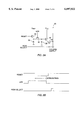
- FIGS. 1A and 2A illustrate typical CMOS active pixel sensors without and with embedded storage, respectively.
- a photodiode 12 employed to collect charge has an anode connected to a fixed voltage potential, shown as ground, and a cathode connected to the source of an N-channel MOS reset transistor 14 and the gate of an N-channel MOS readout transistor 16.
- the gate of N-channel MOS reset transistor 14 is connected to a RESET line, and the drain of N-channel MOS reset transistor 14 is connected to a voltage reference, Vref.
- the drain of N-channel MOS readout transistor 16 is connected to a fixed potential Vcc, and the drain of N-channel MOS readout transistor 16 is connected to an N-channel MOS row select transistor 18.
- the voltage Vref and the voltage Vcc are the same.
- the capacitance available for the integration of the charge sensed by the active pixel sensor 10 includes the photodiode 12 capacitance and the gate capacitance of the N-channel MOS readout transistor 16.
- the operation of the active pixel sensor 10 as it is typically performed is well understood by those of ordinary skill in the art.
- a timing diagram corresponding to the operation of active pixel sensor 10 is depicted FIG. 1B.
- the active pixel sensor 10 is first reset by a RESET signal, during a reset step, that turns on N-channel MOS reset transistor 14 to place the voltage Vref on the cathode of the photodiode 12.
- An integration step begins when the RESET signal makes a transition from HIGH to LOW wherein photo-generated electrons are collected on the photodiode 12 to reduce the voltage on the cathode of the photodiode 12 from the value Vref placed there during the reset step.
- a ROW SELECT signal will be asserted to turn on N-channel MOS select transistor 18 to place the voltage at the source of N-channel MOS readout transistor 16 on the column output line for detection. It should be appreciated that the voltage on the gate of N-channel MOS readout transistor 16 formed by the charge accumulated on the cathode of the photodiode 12 will be followed by the source of N-channel MOS readout transistor 16.
- the CMOS active pixel sensor 30 has embedded storage.
- the active pixel sensor 30 includes a photodiode 32 having an anode that is connected to ground and a cathode that is connected to the source of N-channel MOS reset transistor 34.
- the gate of N-channel MOS reset transistor is connected to a RESET line, and the drain of N-channel MOS reset transistor 34 is connected to a voltage Vref.
- the cathode of photodiode 32 is also connected to the source of N-channel MOS transfer transistor 36.
- the gate of N-channel MOS transfer transistor 36 is connected to a XFR line, and the drain of N-channel MOS transfer transistor 36 is connected to a first plate of a capacitor 38 and to the gate of N-channel MOS readout transistor 40.
- the drain of N-channel MOS readout transistor 40 is connected to Vcc, and the source of N-channel MOS readout transistor 40 is connected to N-channel MOS select transistor 42.
- the voltage Vref and the voltage Vcc are equal to one another.
- the capacitance available for the integration of the charge sensed by the active pixel sensor 30 includes the capacitance of a photodiode 32, the capacitance of the storage capacitor 38, and the gate capacitance of the N-Channel MOS readout transistor 40. It should be appreciated, however, that because the voltage at the drain of the N-channel MOS readout transistor 40 is high, the capacitance at the gate of the N-channel MOS readout transistor 40 is small and the gate capacitance of the N-channel MOS readout transistor 40 is not typically a preferred charge storage element.
- FIG. 2B A timing diagram corresponding to the operation of active pixel sensor 30 is depicted FIG. 2B.
- the N-channel MOS transistor 34 turned on by a RESET signal to place the voltage Vref at the cathode of the photodiode 32
- the N-channel MOS transfer transistor is also turned on by a signal asserted on the XFR line.
- the N-channel MOS reset transistor 34 is turned off, the integration of photons striking the photodiode 32 begins. Since the N-channel MOS transfer transistor 36 is turned on, the capacitor 38 adds to the capacitance of the photodiode 32 during integration to increase the charge capacity and therefore, the intensity range of the storage pixel sensor 30.
- the N-channel MOS transfer transistor 36 is turned off and the N-channel MOS row select transistor 42 is subsequently turned on so that the voltage at the gate of the N-channel MOS readout transistor 40 will be followed by the source of N-channel MOS readout transistor 40 to be placed on the column output.
- the area provided to the photodiodes 12 and 32, respectively can be made larger to improve the sensitivity by increasing the fill factor, and reducing the area for capacitance.
- the noise in the N-channel MOS readout transistors 18 and 40 increases by an amount that is roughly in an inverse proportion to the gate areas of the N-channel MOS readout transistors 16 and 40.
- the gate area of the N-channel MOS readout transistors 16 and 40 is made smaller, the noise increases, and when the gate area of the N-channel MOS readout transistors 16 and 40 is made larger, the noise decreases.
- the sensitivity and noise issues are made more acute.
- the sensitivity is reduced because storage element 38 further reduces the fill factor, and the noise is increased because it reduces the available space for the N-channel MOS readout transistor 40.
- the sensitivity of an active pixel sensor is increased by increasing the fill factor
- the noise of an active pixel sensor is reduced by increasing the relative size of the readout transistor
- the gain is compressive as the relative light intensity in an active pixel sensor increases.
- an active pixel sensor includes a photodiode, a reset transistor, and a readout transistor.
- the photodiode has an anode and a cathode, wherein the anode is connected to a first reference potential.
- the reset transistor has a gate, a source and a drain, wherein the gate is connected to a reset line, the drain is connected to a second reference potential greater than the first reference potential, and the source is connected to the cathode of the photodiode.
- the readout transistor has a gate, a source, and a drain,wherein the gate is connected to the cathode of the photodiode, and the drain is connected to a switchable supply voltage.
- an active pixel sensor in a second embodiment, includes a photodiode, a reset transistor, a transfer transistor, and a readout transistor.
- the photodiode has an anode and a cathode, wherein the anode is connected to a first reference potential.
- the reset transistor has a gate, a source and a drain, wherein the gate is connected to a reset line, the drain is connected to a second reference potential greater than the first reference potential, and the source is connected to the cathode of the photodiode.
- the transfer transistor has a gate, a first drain/source, and a second drain/source, wherein the gate is connected to a transfer line and the first drain/source is connected to the cathode of the photodiode.
- the readout transistor has a gate, a source, and a drain, wherein the gate is connected to the second drain/source of the transfer transistor, and the drain is connected to a switchable supply voltage.
- the voltage at the drain of the readout transistor of an active pixel sensor is held at a low level during the integration period of the active pixel sensor, and is brought to a high level or pulsed to a high level in synchronism with the row select signals during the readout period.
- FIG. 1A illustrates a simplified schematic of a first known active pixel sensor.
- FIG. 1B is a timing diagram corresponding to the operation of the active pixel sensor depicted in FIG. 1A.
- FIG. 2A illustrates a simplified schematic of a second known active pixel sensor.
- FIG. 2B is a timing diagram corresponding to the operation of the active pixel sensor depicted in FIG. 2A.
- FIG. 3A illustrates a simplified schematic of a first embodiment of an active pixel sensor according to the present invention.
- FIG. 3B is a timing diagram corresponding to the operation of the active pixel sensor depicted in FIG. 3A.
- FIG. 4A illustrates a simplified schematic of a second embodiment of an active pixel sensor according to the present invention.
- FIG. 4B is a timing diagram corresponding to the operation of the active pixel sensor depicted in FIG. 4A.
- FIG. 5 illustrates the gate, drain, source, and back-gates voltages in a readout transistor during integration and readout in a first example according to the present invention.
- FIG. 6 illustrates the gate, drain, source, and back-gates voltages in a readout transistor during integration and readout in a second example according to the present invention.
- FIG. 7 illustrates the gate, drain, source, and back-gates voltages in a readout transistor during integration and readout in a third example according to the present invention.
- FIG. 8 illustrates compression in the gain of an active pixel sensor as the relative light intensity increases according to the present invention.
- FIGS. 3A and 4A first and second embodiments of active pixel sensors 50 and 60, respectively, according to the present invention are depicted.
- the active pixel sensor 50 in FIG. 3A is similar to the active pixel sensor 10 of FIG. 1A, and accordingly, the same reference numerals are employed.
- Active pixel sensor 50 differs from active pixel sensor 10 in the important aspect that the drain of the N-channel MOS readout transistor 18 is connected to a switchable supply voltage Vd.
- FIG. 3B A timing diagram corresponding to the operation of active pixel sensor 50 is depicted FIG. 3B.
- the RESET signal is first at a HIGH level to turn on the N-channel MOS reset transistor 14 and thereby set the cathode of photodiode 12 at Vref.
- the RESET signal makes a transition from HIGH to LOW at falling edge 52, the integration of photocharge as described above begins.
- the supply voltage Vd at the drain of the N-channel MOS readout transistor 16 is switched to make a transition from LOW to HIGH.
- the supply voltage Vd may either be brought HIGH during the entire readout, as illustrated by dashed line 54 or it may be brought HIGH when each of the ROW SELECT signals 56-1 through 56-n is asserted.
- the ROW SELECT 1 through n lines are connected to rows of the active pixel sensors 50 in a manner understood by those of ordinary skill in the art.
- the ROW SELECT signals 56-1 through 56-n are asserted the images stored in the respective active pixel sensors 50 for each of the rows will be read out in a manner similar to that described above.
- the active pixel sensor 60 depicted in FIG. 4A according to the present invention is similar to the active pixel sensor 30 in FIG. 2A. Accordingly, the same reference numerals employed in FIG. 2A are also employed in FIG. 4A.
- the active pixel sensor 60 differs from the active pixel sensor 30 in two important aspects. First, the separate storage capacitor 38 present in the active pixel sensor 30 is not needed in the active pixel sensor 60, and the drain of N-channel MOS readout transistor 38 is connected to a switchable supply voltage Vd. Further, the voltage Vref is a lower voltage than that found in the prior art.
- FIG. 4B A timing diagram corresponding to the operation of active pixel sensor 60 is depicted in FIG. 4B.
- the N-channel MOS transfer transistor 34 turned on by a HIGH RESET signal to place the voltage Vref at the cathode of the photodiode 32
- the N-channel MOS transfer transistor is also turned on by a HIGH signal asserted on the XFR line.
- the N-channel MOS reset transistor 34 is turned off by the RESET signal making a transition 62 from HIGH to LOW, the integration of photons striking the photodiode 32 begins.
- the N-channel MOS transfer transistor 36 is turned off.
- the supply voltage Vd may either be brought HIGH during the entire readout, as illustrated by dashed line 64 or it may be brought HIGH when each of the ROW SELECT signals 66-1 through 66-n is asserted.
- the ROW SELECT signals 66-1 through 66-n are asserted the images stored in the respective active pixel sensors 60 for each of the rows will be read out.
- the drain of the N-channel MOS readout transistors 16 and 40 is set to a first voltage level, preferably near ground, during the integration period, and then set to a second voltage level, preferably greater than Vref, during the readout period.
- the gates of the N-channel MOS readout transistors 16 and 40 in active pixel sensors 50 and 60 respectively, operate as large nonlinear capacitors during the charge integration period, and as small and nearly linear capacitors during the readout period.
- the N-channel MOS readout transistors 16 and 40 When the sources of the N-channel MOS readout transistors 16 and 40, respectively, are set near ground, the N-channel MOS readout transistors 16 and 40 will be turned on. As such, the gates of N-channel MOS read out transistors 16 and 40 provide a large capacitance. During integration, the large on-state capacitance at the gates of N-channel MOS readout transistors 16 and 40 is connected in parallel with, and therefore adds to, the capacitance of the photodiodes 12 and 32, respectively. This increased capacitance decreases the charge-to-voltage gain during the integration period.
- N-channel MOS readout transistor 40 Since the gate of N-channel MOS readout transistor 40 is boosted to a higher level during readout, a voltage Vref that is lower than that found in the prior art is preferred. As a consequence, the logic high voltage level on the RESET signal line may also be reduced.
- the sensitivity of the active pixel sensor 60 may be increased by enlarging the area available to the photodiode 32 without a loss of the photocharge generated due to the large on-state capacitance of the gate of N-channel MOS readout transistor 40.
- the photo-generated charge can no longer be held on the gate of N-channel MOS readout transistor 16, so it is held instead on the capacitance of photodiode 12. Since the net capacitance is lower, the charge-to-voltage gain is higher.
- the bootstrapping action can be viewed as reducing the capacitance to get a higher voltage signal on the photodiode 12, and then reading out that signal according to the gain of N-channel MOS readout transistor 16 operating as a source follower.
- the effect of the bootstrap action is both beneficial and surprising.
- the N-channel MOS transfer transistor 36 is turned off by the control signal on the XFR line.
- the gate capacitance of N-channel MOS readout transistor 40 becomes small during readout, the area to which the photo-generated charge may be redistributed is small. That is, the associated stray capacitance of the circuit node that includes the source/drain terminal of N-channel MOS transfer transistor 36 and the gate terminal of N-channel MOS readout transistor 40 is quite small, compared to the photodiode 12 capacitance. This greatly reduced capacitance leads to an increased charge-to-voltage gain.
- the limit on the achievable charge-to-voltage gain is determined by the linear combination of the voltage at the gate of N-channel MOS readout transistor 40, and the back-gate or substrate voltage of the N-channel MOS readout transistor 40 that is needed to place the N-channel MOS readout transistor 40 at threshold.
- the resulting conversion is a nearly linear function of the charge signal that was captured on the storage node at the gate of N-channel MOS readout transistor 40.
- the gate capacitance of N-channel MOS readout transistors 16 and 40 couple primarily to the sources when the drains of N-channel MOS readout transistors 16 and 40 are brought high so that the gate to source capacitance C GS dominates the gate to drain capacitance C GD .
- the stray storage node capacitance is represented by C S . Though this capacitance may be relevant, it may be small in the active pixel 60.
- V G V GO + ⁇ V G
- the bootstrapped gate voltage of N-channel MOS readout transistors 16 and 40 may be expressed as: ##EQU1##
- the column output voltage may be expressed as the source voltage as follows: ##EQU2## This implies that the gain from the signal initially stored at the gate of N-channel MOS readout transistors 16 and 40 to the column output during read out is expressed by the following relation: ##EQU3## wherein the approximation holds for small values of C GD and C S .
- the linear conversion of captured charge to a final voltage on the column output line has two beneficial consequences.
- a large capacitance value at the gate of N-channel MOS readout transistor 40 has a beneficial, rather than a harmful, effect on the overall gain, since a larger capacitance on that side of the N-channel MOS transfer transistor 36 means that a larger fraction of the photocharge is captured, as opposed to being wasted charging the photodiode 32 itself.
- the overall gain will typically exceed even the gain of the photodiode 32 without any additional capacitive loading. Therefore, increasing the N-channel MOS readout transistor 40 size to reduce noise will not substantially reduce the gain.
- the linear conversion from captured charge to output voltage can lead to a beneficial compressive non-linearity as follows. As photocharge is accumulated, the gate of N-channel MOS readout transistor 40 will fall in voltage until at some point it falls below a threshold voltage, at which point the gate capacitance will change from high to low. Further photocharge will accumulate primarily on the photodiode 32 capacitance only, so the voltage at the gate of N-channel MOS readout transistor 40 will fall more quickly.
- This charge-to-voltage break-point non-linearity during integration is expansive, not compressive, but nonetheless leads surprisingly to a compressive break-point non-linearity in the overall gain.
- the N-channel MOS transfer transistor 36 When the N-channel MOS transfer transistor 36 is turned off, the proportion of charge stored on the storage side of the N-channel MOS transfer transistor 36 is reduced at high light levels, since more of that charge is kept on the photodiode 32 instead. Hence the integrated image signal voltage responds expansively during integration, yet a linear readout of the stored charge responds compressively.
- FIGS. 5, 6, and 7 examples of the voltages found on N-channel MOS readout transistors 16 and 40 during the integration period and readout periods for different light intensities are illustrated.
- the voltages correspond to increasing intensity conditions, as the light goes from darker to a lighter.
- the voltage at both the drain and the source of the readout transistor are both at ground, and by convention the substrate or back-gate potential is also referred to as ground.
- the voltages at the gate of the readout transistor at the end of the integration period are 1.5, 0.6, and 0.2 volts, respectively. Since, in this example, the Vref to which the photodiode is initially set is 1.5 volts, the 1.5 volts at the gate of the readout transistor in FIG. 5 corresponds to a dark condition, and the 0.2 volts at the gate of the readout transistor in FIG. 7 corresponds to a lighter condition than the 0.6 volts at the gate of the readout transistor in FIG. 6.
- the value of kappa, ⁇ , described above is two-thirds, and V TH is 0.6 volts.
- the output source voltage will settle such that two-thirds of the gate-to-source voltage, V GS , added to one-third of the bulk-to-source voltage, V BS , will be equal to approximately 0.4 volts.
- this provides source voltages of 1.7, 0.2, and nearly 0 volts, respectively.
- FIG. 8 the voltage depicted for the differing light conditions in FIGS. 5, 6, and 7 for the source during readout is illustrated graphically. From FIG. 8, those of ordinary skill in the art will readily appreciate that according to the present invention, the gain is compressed as the relative intensity in the light increases. This can be observed from the graph of the voltage Vs at the source during readout by comparing area A in the graph with area B in the graph. Area A of the graph of Vs has a first slope, and area B of the graph of Vs has a second slope such that the slope of area B has an absolute value that is less than the absolute value of the slope in area A. This change in the slope of the graph of Vs as the relative light intensity increases corresponds to a compression in the gain. The dashed line indicates that the gain becomes even more compressive than is demonstrated by slope of area B. This further compression is due to subthreshold effects, the discussion of which is beyond the scope of this disclosure.
Abstract
In a first embodiment an active pixel sensor includes a photodiode for capturing photocharge, a reset transistor for resetting the photodiode to a reset potential, and a readout transistor, and in a second embodiment an active pixel sensor includes a photodiode for capturing photocharge, a reset transistor for resetting the photodiode to a reset potential, a transfer transistor for transferring captured photocharge, and a readout transistor. In both embodiments, the readout transistor has a drain that is coupled to a first supply voltage during integration of photocharge and a second supply voltage during readout of the photocharge. Accordingly, the sensitivity of an active pixel sensor is increased by increasing the fill factor, the noise an active pixel sensor is reduced by increasing the relative size of the readout transistor, and the gain is compressive as the relative light intensity in an active pixel sensor increases.
Description
1. Field of the Invention
The present invention relates to active pixel sensors. More particularly, the present invention relates to variable biasing of the readout transistor in an active pixel sensor to improve sensitivity, reduce noise and to provide compressive non-linearity in the charge-to-voltage gain.
2. The Prior Art
In the art of CMOS active pixel sensors, the sensitivity, noise, and nature of the gain of an active pixel sensor present issues of concern. The sensitivity of an active pixel sensor in measuring the charge generated by the photons striking the active pixel sensor is typically characterized by determining the volts generated per photon of light striking the active pixel sensor and is termed charge-to-voltage gain. The readout amplifier in an active pixel sensor represents a substantial source of noise that in prior art pixel sensors has required design tradeoffs. The gain in prior art active pixel sensors is most often expansive, though it is preferred to be compressive.
The sensitivity of an active pixel sensor is determined by at least three factors. The first factor is related to the percentage of the area in the active pixel sensor available for converting photons to electrons. This is known as the fill factor. An increase in the area leads to an increase in the amount of charge generated. A second factor affecting the sensitivity of the active pixel sensor is related to the capacitance that is available for the integration of the charge sensed by the active pixel sensor. It will be appreciated that the voltage on the capacitor for given amount of charge is inversely proportional to the size of the capacitor. Accordingly, when the capacitance increases, the voltage decreases for the same amount of charge. A third factor is the gain of the readout amplifier for the active pixel sensor. Since the readout amplifier in the prior art is typically a transistor configured as a source follower, the gain is less than one.
One source of noise in an active pixel sensor is created by threshold fluctuations in the readout transistor. The amount of threshold fluctuation is related to the size of the readout transistor. As the size of the readout transistor is increased, the amount of threshold fluctuation, and hence the amount of noise decreases.
In compressive nonlinear gain, the gain at high light levels is less than the gain at low light levels. Those of ordinary skill in the art will appreciate that it is typically desirable to have greater sensitivity in converting photons-to-voltage at lower rather than higher light levels, because this increases the signal-to-noise ratio at lower light levels and, accordingly, the usable dynamic range of the active pixel sensor is increased.
The CMOS active pixel sensor art includes active pixel sensors that may or may not have embedded storage. FIGS. 1A and 2A illustrate typical CMOS active pixel sensors without and with embedded storage, respectively.
In an active pixel sensor 10 of FIG. 1A, a photodiode 12 employed to collect charge has an anode connected to a fixed voltage potential, shown as ground, and a cathode connected to the source of an N-channel MOS reset transistor 14 and the gate of an N-channel MOS readout transistor 16. The gate of N-channel MOS reset transistor 14 is connected to a RESET line, and the drain of N-channel MOS reset transistor 14 is connected to a voltage reference, Vref. The drain of N-channel MOS readout transistor 16 is connected to a fixed potential Vcc, and the drain of N-channel MOS readout transistor 16 is connected to an N-channel MOS row select transistor 18. Typically, the voltage Vref and the voltage Vcc are the same. In the active pixel sensor 10, the capacitance available for the integration of the charge sensed by the active pixel sensor 10 includes the photodiode 12 capacitance and the gate capacitance of the N-channel MOS readout transistor 16.
The operation of the active pixel sensor 10 as it is typically performed is well understood by those of ordinary skill in the art. A timing diagram corresponding to the operation of active pixel sensor 10 is depicted FIG. 1B. The active pixel sensor 10 is first reset by a RESET signal, during a reset step, that turns on N-channel MOS reset transistor 14 to place the voltage Vref on the cathode of the photodiode 12. An integration step begins when the RESET signal makes a transition from HIGH to LOW wherein photo-generated electrons are collected on the photodiode 12 to reduce the voltage on the cathode of the photodiode 12 from the value Vref placed there during the reset step. During a readout step, a ROW SELECT signal will be asserted to turn on N-channel MOS select transistor 18 to place the voltage at the source of N-channel MOS readout transistor 16 on the column output line for detection. It should be appreciated that the voltage on the gate of N-channel MOS readout transistor 16 formed by the charge accumulated on the cathode of the photodiode 12 will be followed by the source of N-channel MOS readout transistor 16.
In FIG. 2A, the CMOS active pixel sensor 30 has embedded storage. The active pixel sensor 30 includes a photodiode 32 having an anode that is connected to ground and a cathode that is connected to the source of N-channel MOS reset transistor 34. The gate of N-channel MOS reset transistor is connected to a RESET line, and the drain of N-channel MOS reset transistor 34 is connected to a voltage Vref. The cathode of photodiode 32 is also connected to the source of N-channel MOS transfer transistor 36. The gate of N-channel MOS transfer transistor 36 is connected to a XFR line, and the drain of N-channel MOS transfer transistor 36 is connected to a first plate of a capacitor 38 and to the gate of N-channel MOS readout transistor 40. The drain of N-channel MOS readout transistor 40 is connected to Vcc, and the source of N-channel MOS readout transistor 40 is connected to N-channel MOS select transistor 42. Typically, the voltage Vref and the voltage Vcc are equal to one another.
In the active pixel sensor 30, the capacitance available for the integration of the charge sensed by the active pixel sensor 30 includes the capacitance of a photodiode 32, the capacitance of the storage capacitor 38, and the gate capacitance of the N-Channel MOS readout transistor 40. It should be appreciated, however, that because the voltage at the drain of the N-channel MOS readout transistor 40 is high, the capacitance at the gate of the N-channel MOS readout transistor 40 is small and the gate capacitance of the N-channel MOS readout transistor 40 is not typically a preferred charge storage element.
A timing diagram corresponding to the operation of active pixel sensor 30 is depicted FIG. 2B. In the operation of the active pixel sensor 30, with the N-channel MOS transistor 34 turned on by a RESET signal to place the voltage Vref at the cathode of the photodiode 32, the N-channel MOS transfer transistor is also turned on by a signal asserted on the XFR line. When the N-channel MOS reset transistor 34 is turned off, the integration of photons striking the photodiode 32 begins. Since the N-channel MOS transfer transistor 36 is turned on, the capacitor 38 adds to the capacitance of the photodiode 32 during integration to increase the charge capacity and therefore, the intensity range of the storage pixel sensor 30. At the end of the integration period, the N-channel MOS transfer transistor 36 is turned off and the N-channel MOS row select transistor 42 is subsequently turned on so that the voltage at the gate of the N-channel MOS readout transistor 40 will be followed by the source of N-channel MOS readout transistor 40 to be placed on the column output.
In both active pixel sensors 10 and 30, by minimizing the gate area of the N-channel MOS readout transistors 16 and 40, respectively, the area provided to the photodiodes 12 and 32, respectively, can be made larger to improve the sensitivity by increasing the fill factor, and reducing the area for capacitance. Unfortunately, in reducing the gate capacitance of the N-channel MOS readout transistors 16 and 40, the noise in the N-channel MOS readout transistors 18 and 40 increases by an amount that is roughly in an inverse proportion to the gate areas of the N-channel MOS readout transistors 16 and 40. As such, when the gate area of the N-channel MOS readout transistors 16 and 40 is made smaller, the noise increases, and when the gate area of the N-channel MOS readout transistors 16 and 40 is made larger, the noise decreases.
In the case of the active pixel sensor 30, wherein the storage element 38 is included as a separate element, the sensitivity and noise issues are made more acute. The sensitivity is reduced because storage element 38 further reduces the fill factor, and the noise is increased because it reduces the available space for the N-channel MOS readout transistor 40.
Accordingly, it is an object of the present invention to increase the sensitivity of an active pixel sensor.
It is a further object of the present invention to decease the noise of an active pixel sensor.
It is yet another object of the present invention to compress the gain in an active pixel sensor as the relative light intensity increases.
According to the present invention, the sensitivity of an active pixel sensor is increased by increasing the fill factor, the noise of an active pixel sensor is reduced by increasing the relative size of the readout transistor, and the gain is compressive as the relative light intensity in an active pixel sensor increases.
In a first embodiment, an active pixel sensor includes a photodiode, a reset transistor, and a readout transistor. The photodiode has an anode and a cathode, wherein the anode is connected to a first reference potential. The reset transistor has a gate, a source and a drain, wherein the gate is connected to a reset line, the drain is connected to a second reference potential greater than the first reference potential, and the source is connected to the cathode of the photodiode. The readout transistor has a gate, a source, and a drain,wherein the gate is connected to the cathode of the photodiode, and the drain is connected to a switchable supply voltage.
In a second embodiment, an active pixel sensor includes a photodiode, a reset transistor, a transfer transistor, and a readout transistor. The photodiode has an anode and a cathode, wherein the anode is connected to a first reference potential. The reset transistor has a gate, a source and a drain, wherein the gate is connected to a reset line, the drain is connected to a second reference potential greater than the first reference potential, and the source is connected to the cathode of the photodiode. The transfer transistor has a gate, a first drain/source, and a second drain/source, wherein the gate is connected to a transfer line and the first drain/source is connected to the cathode of the photodiode. The readout transistor has a gate, a source, and a drain, wherein the gate is connected to the second drain/source of the transfer transistor, and the drain is connected to a switchable supply voltage.
In a method according to the present invention, the voltage at the drain of the readout transistor of an active pixel sensor is held at a low level during the integration period of the active pixel sensor, and is brought to a high level or pulsed to a high level in synchronism with the row select signals during the readout period.
FIG. 1A illustrates a simplified schematic of a first known active pixel sensor.
FIG. 1B is a timing diagram corresponding to the operation of the active pixel sensor depicted in FIG. 1A.
FIG. 2A illustrates a simplified schematic of a second known active pixel sensor.
FIG. 2B is a timing diagram corresponding to the operation of the active pixel sensor depicted in FIG. 2A.
FIG. 3A illustrates a simplified schematic of a first embodiment of an active pixel sensor according to the present invention.
FIG. 3B is a timing diagram corresponding to the operation of the active pixel sensor depicted in FIG. 3A.
FIG. 4A illustrates a simplified schematic of a second embodiment of an active pixel sensor according to the present invention.
FIG. 4B is a timing diagram corresponding to the operation of the active pixel sensor depicted in FIG. 4A.
FIG. 5 illustrates the gate, drain, source, and back-gates voltages in a readout transistor during integration and readout in a first example according to the present invention.
FIG. 6 illustrates the gate, drain, source, and back-gates voltages in a readout transistor during integration and readout in a second example according to the present invention.
FIG. 7 illustrates the gate, drain, source, and back-gates voltages in a readout transistor during integration and readout in a third example according to the present invention.
FIG. 8 illustrates compression in the gain of an active pixel sensor as the relative light intensity increases according to the present invention.
Those of ordinary skill in the art will realize that the following description of the present invention is illustrative only and not in any way limiting. Other embodiments of the invention will readily suggest themselves to such skilled persons.
In FIGS. 3A and 4A, first and second embodiments of active pixel sensors 50 and 60, respectively, according to the present invention are depicted. The active pixel sensor 50 in FIG. 3A is similar to the active pixel sensor 10 of FIG. 1A, and accordingly, the same reference numerals are employed. Active pixel sensor 50 differs from active pixel sensor 10 in the important aspect that the drain of the N-channel MOS readout transistor 18 is connected to a switchable supply voltage Vd.
A timing diagram corresponding to the operation of active pixel sensor 50 is depicted FIG. 3B. In the operation of active pixel sensor 50, the RESET signal is first at a HIGH level to turn on the N-channel MOS reset transistor 14 and thereby set the cathode of photodiode 12 at Vref. When the RESET signal makes a transition from HIGH to LOW at falling edge 52, the integration of photocharge as described above begins. During a readout step, in contrast to the prior art, the supply voltage Vd at the drain of the N-channel MOS readout transistor 16 is switched to make a transition from LOW to HIGH. According to the present invention, the supply voltage Vd may either be brought HIGH during the entire readout, as illustrated by dashed line 54 or it may be brought HIGH when each of the ROW SELECT signals 56-1 through 56-n is asserted. It should be appreciated that the ROW SELECT 1 through n lines are connected to rows of the active pixel sensors 50 in a manner understood by those of ordinary skill in the art. When the ROW SELECT signals 56-1 through 56-n are asserted the images stored in the respective active pixel sensors 50 for each of the rows will be read out in a manner similar to that described above.
The active pixel sensor 60 depicted in FIG. 4A according to the present invention is similar to the active pixel sensor 30 in FIG. 2A. Accordingly, the same reference numerals employed in FIG. 2A are also employed in FIG. 4A. The active pixel sensor 60, according to the present invention, differs from the active pixel sensor 30 in two important aspects. First, the separate storage capacitor 38 present in the active pixel sensor 30 is not needed in the active pixel sensor 60, and the drain of N-channel MOS readout transistor 38 is connected to a switchable supply voltage Vd. Further, the voltage Vref is a lower voltage than that found in the prior art.
A timing diagram corresponding to the operation of active pixel sensor 60 is depicted in FIG. 4B. In the operation of the active pixel sensor 60, with the N-channel MOS transistor 34 turned on by a HIGH RESET signal to place the voltage Vref at the cathode of the photodiode 32, the N-channel MOS transfer transistor is also turned on by a HIGH signal asserted on the XFR line. When the N-channel MOS reset transistor 34 is turned off by the RESET signal making a transition 62 from HIGH to LOW, the integration of photons striking the photodiode 32 begins. To end the integration period, the N-channel MOS transfer transistor 36 is turned off. According to the present invention, during a readout period the supply voltage Vd may either be brought HIGH during the entire readout, as illustrated by dashed line 64 or it may be brought HIGH when each of the ROW SELECT signals 66-1 through 66-n is asserted. When the ROW SELECT signals 66-1 through 66-n are asserted the images stored in the respective active pixel sensors 60 for each of the rows will be read out.
In the operation of the storage pixels 50 and 60 according to the present invention as described, there is a reset period, an integration period, and a read out period. However, unlike the operation of prior art active pixel sensors, the drain of the N-channel MOS readout transistors 16 and 40, respectively, is set to a first voltage level, preferably near ground, during the integration period, and then set to a second voltage level, preferably greater than Vref, during the readout period. Pursuant to these biasing conditions, the gates of the N-channel MOS readout transistors 16 and 40 in active pixel sensors 50 and 60, respectively, operate as large nonlinear capacitors during the charge integration period, and as small and nearly linear capacitors during the readout period.
When the sources of the N-channel MOS readout transistors 16 and 40, respectively, are set near ground, the N-channel MOS readout transistors 16 and 40 will be turned on. As such, the gates of N-channel MOS read out transistors 16 and 40 provide a large capacitance. During integration, the large on-state capacitance at the gates of N-channel MOS readout transistors 16 and 40 is connected in parallel with, and therefore adds to, the capacitance of the photodiodes 12 and 32, respectively. This increased capacitance decreases the charge-to-voltage gain during the integration period.
However, when the drains of N-channel MOS readout transistors 16 and 40 are brought high during the readout period, the change in the variable supply voltage Vd boosts the voltage on the gate via a "bootstrap" capacitive coupling effect well known to those of ordinary skill in the art, and the decrease in the charge-to-voltage gain realized during the integration period described above will typically be compensated for by the increased readout gain that comes from the bootstrapping dynamics when the drains of N-channel MOS readout transistors 16 and 40 are brought high. This bootstrap effect provides a large operating range of the output signal voltages. Accordingly, this biasing scheme according to the present invention increases the sensitivity of the active pixel sensors.
Since the gate of N-channel MOS readout transistor 40 is boosted to a higher level during readout, a voltage Vref that is lower than that found in the prior art is preferred. As a consequence, the logic high voltage level on the RESET signal line may also be reduced.
In contrast to the prior art, because the storage element 38 shown in FIG. 2A has been eliminated from the active pixel sensor 60 as depicted in FIG. 4A, the sensitivity of the active pixel sensor 60 may be increased by enlarging the area available to the photodiode 32 without a loss of the photocharge generated due to the large on-state capacitance of the gate of N-channel MOS readout transistor 40.
Since raising the variable supply voltage Vd to the drains of N- channel MOS transistors 16 and 40 and letting the source terminals settle upward causes the gate capacitance of N-channel MOS readout transistors 16 and 40 to change from a high capacitance to a low capacitance, it will be appreciated that there will be a corresponding redistribution of charge and voltage values within the active pixel sensors 50 and 60.
During the readout period of active pixel sensor 50, the photo-generated charge can no longer be held on the gate of N-channel MOS readout transistor 16, so it is held instead on the capacitance of photodiode 12. Since the net capacitance is lower, the charge-to-voltage gain is higher. The bootstrapping action can be viewed as reducing the capacitance to get a higher voltage signal on the photodiode 12, and then reading out that signal according to the gain of N-channel MOS readout transistor 16 operating as a source follower.
During the readout period of active pixel sensor 60, the effect of the bootstrap action is both beneficial and surprising. After accumulating charge during the integration period, the N-channel MOS transfer transistor 36 is turned off by the control signal on the XFR line. When the gate capacitance of N-channel MOS readout transistor 40 becomes small during readout, the area to which the photo-generated charge may be redistributed is small. That is, the associated stray capacitance of the circuit node that includes the source/drain terminal of N-channel MOS transfer transistor 36 and the gate terminal of N-channel MOS readout transistor 40 is quite small, compared to the photodiode 12 capacitance. This greatly reduced capacitance leads to an increased charge-to-voltage gain.
The limit on the achievable charge-to-voltage gain is determined by the linear combination of the voltage at the gate of N-channel MOS readout transistor 40, and the back-gate or substrate voltage of the N-channel MOS readout transistor 40 that is needed to place the N-channel MOS readout transistor 40 at threshold. The resulting conversion is a nearly linear function of the charge signal that was captured on the storage node at the gate of N-channel MOS readout transistor 40.
It should be appreciated that when the column output and the sources of the N-channel MOS read out transistors 18 and 40 settle, the N-channel MOS read out transistors 18 and 40 will be near threshold. The voltage at the source, taking into account the body effect, κ, is expressed by the following relation:
V.sub.S =κ(V.sub.G -V.sub.Th)
Accordingly, the two unknowns, the source and the gate voltages of N-channel MOS readout transistors 16 and 40 are linearly related.
The expression of charge conservation at the gate of the N-channel MOS readout transistors 16 and 40 which provides a further constraint is as follows:
(ΔV.sub.S -ΔV.sub.G)C.sub.GS +(ΔV.sub.D -ΔV.sub.G)C.sub.GD =ΔV.sub.G C.sub.S
In this expression, assuming linear capacitances, the gate capacitance of N-channel MOS readout transistors 16 and 40 couple primarily to the sources when the drains of N-channel MOS readout transistors 16 and 40 are brought high so that the gate to source capacitance CGS dominates the gate to drain capacitance CGD. The stray storage node capacitance is represented by CS. Though this capacitance may be relevant, it may be small in the active pixel 60.
Defining a gate voltage VGO before bringing VD high, and a final gate voltage VG, such that: VG =VGO +ΔVG, and assuming VD and VS are initially at ground so that VS =ΔVS and VD =ΔVD, the bootstrapped gate voltage of N-channel MOS readout transistors 16 and 40 may be expressed as: ##EQU1##
As a result, the column output voltage may be expressed as the source voltage as follows: ##EQU2## This implies that the gain from the signal initially stored at the gate of N-channel MOS readout transistors 16 and 40 to the column output during read out is expressed by the following relation: ##EQU3## wherein the approximation holds for small values of CGD and CS.
The linear conversion of captured charge to a final voltage on the column output line has two beneficial consequences. First, it means that a large capacitance value at the gate of N-channel MOS readout transistor 40 has a beneficial, rather than a harmful, effect on the overall gain, since a larger capacitance on that side of the N-channel MOS transfer transistor 36 means that a larger fraction of the photocharge is captured, as opposed to being wasted charging the photodiode 32 itself. The overall gain will typically exceed even the gain of the photodiode 32 without any additional capacitive loading. Therefore, increasing the N-channel MOS readout transistor 40 size to reduce noise will not substantially reduce the gain.
Second, the linear conversion from captured charge to output voltage can lead to a beneficial compressive non-linearity as follows. As photocharge is accumulated, the gate of N-channel MOS readout transistor 40 will fall in voltage until at some point it falls below a threshold voltage, at which point the gate capacitance will change from high to low. Further photocharge will accumulate primarily on the photodiode 32 capacitance only, so the voltage at the gate of N-channel MOS readout transistor 40 will fall more quickly. This charge-to-voltage break-point non-linearity during integration is expansive, not compressive, but nonetheless leads surprisingly to a compressive break-point non-linearity in the overall gain. When the N-channel MOS transfer transistor 36 is turned off, the proportion of charge stored on the storage side of the N-channel MOS transfer transistor 36 is reduced at high light levels, since more of that charge is kept on the photodiode 32 instead. Hence the integrated image signal voltage responds expansively during integration, yet a linear readout of the stored charge responds compressively.
Turning now to FIGS. 5, 6, and 7 examples of the voltages found on N-channel MOS readout transistors 16 and 40 during the integration period and readout periods for different light intensities are illustrated. In FIGS. 5, 6, and 7, the voltages correspond to increasing intensity conditions, as the light goes from darker to a lighter.
As depicted in FIGS. 5, 6, and 7, during the integration period, the voltage at both the drain and the source of the readout transistor are both at ground, and by convention the substrate or back-gate potential is also referred to as ground. In FIGS. 5, 6, and 7, the voltages at the gate of the readout transistor at the end of the integration period are 1.5, 0.6, and 0.2 volts, respectively. Since, in this example, the Vref to which the photodiode is initially set is 1.5 volts, the 1.5 volts at the gate of the readout transistor in FIG. 5 corresponds to a dark condition, and the 0.2 volts at the gate of the readout transistor in FIG. 7 corresponds to a lighter condition than the 0.6 volts at the gate of the readout transistor in FIG. 6.
During the readout period illustrated in FIGS. 5, 6, and 7, the voltage at the drain of the readout transistor is raised by 2 volts. It can be observed that as a result, the voltage at the gate of the readout transistor has increased in each of the three examples. In FIG. 5, a comparison of the gate voltage at the end of the integration period with the gate voltage during the readout period reveals that the voltage at the gate has gone from about 1.5 volts to about 3.15 volts. In FIG. 6, a comparison of the gate voltage at the end of the integration period with the gate voltage during the readout period reveals that the voltage at the gate has gone from about 0.6 volts to about 0.9 volts. In FIG. 7, a comparison of the gate voltage at the end of the integration period with the gate voltage during the readout period reveals that the voltage at the gate has gone from about 0.2 volts to about 0.6 volts. The increase at the gate in these examples is a result of the bootstrap amplification that takes place due to capacitive coupling between the drain and source and the gate of the readout transistor. This increase is generally an amount that is less than the amount that the source of the readout transistor is increased, unless the gate-drain overlap capacitance is significant.
In the examples shown in FIGS. 5, 6, and 7, the value of kappa, κ, described above is two-thirds, and VTH is 0.6 volts. In accordance with the above discussion, the output source voltage will settle such that two-thirds of the gate-to-source voltage, VGS, added to one-third of the bulk-to-source voltage, VBS, will be equal to approximately 0.4 volts. In FIGS. 5, 6, and 7, during the readout period, this provides source voltages of 1.7, 0.2, and nearly 0 volts, respectively.
In FIG. 8, the voltage depicted for the differing light conditions in FIGS. 5, 6, and 7 for the source during readout is illustrated graphically. From FIG. 8, those of ordinary skill in the art will readily appreciate that according to the present invention, the gain is compressed as the relative intensity in the light increases. This can be observed from the graph of the voltage Vs at the source during readout by comparing area A in the graph with area B in the graph. Area A of the graph of Vs has a first slope, and area B of the graph of Vs has a second slope such that the slope of area B has an absolute value that is less than the absolute value of the slope in area A. This change in the slope of the graph of Vs as the relative light intensity increases corresponds to a compression in the gain. The dashed line indicates that the gain becomes even more compressive than is demonstrated by slope of area B. This further compression is due to subthreshold effects, the discussion of which is beyond the scope of this disclosure.
While embodiments and applications of this invention have been shown and described, it would be apparent to those skilled in the art that many more modifications than mentioned above are possible without departing from the inventive concepts herein. The invention, therefore, is not to be restricted except in the spirit of the appended claims.
Claims (6)
1. An active pixel sensor comprising:
a photosensor having a first terminal and a second terminal, said first terminal coupled to a first reference potential;
a reset transistor having a gate, a source and a drain, said gate coupled to a reset line, said drain coupled to a second reference potential, and said source coupled to said second terminal of said photosensor; and
a readout transistor having a gate, a source, and a drain, said gate coupled to said second terminal of said photosensor, and said drain coupled to a switched supply voltage to change capacitance at said gate when said supply voltage is switched.
2. An active pixel sensor as in claim 1, wherein said gate of said readout transistor is coupled to said second terminal of said photodiode by a transfer transistor having a first source/drain coupled to said second terminal of said photosensor, a second source/drain coupled to said gate of said readout transistor, and a gate coupled to a transfer line.
3. A method of operating an active pixel sensor having a photosensor, a reset transistor, a readout transistor, and a row select transistor, said readout transistor having a gate coupled to said photosensor, a drain coupled to a switchable supply voltage, and a source, and said row select transistor having a gate coupled to a row select line, a drain coupled to said source of said readout transistor, and a source, comprising the steps of:
applying a reset signal at a first logic level to said gate of said reset transistor during a reset period to set said photosensor at a reset potential;
applying a reset signal at a second logic level to said gate of said reset transistor during an integration period to begin capture of photocharge;
applying a first supply voltage to said drain of said readout transistor during said integration period to bias said readout transistor to have a first gate capacitance;
applying a row select signal at said gate of said row select transistor during a readout period to output a signal corresponding to said photocharge; and
applying a second supply voltage to said drain of said readout transistor during said readout period to bias said readout transistor to have a second gate capacitance less than said first gate capacitance.
4. The method of operating an active pixel sensor as in claim 2, wherein said second supply voltage is applied approximately in synchronism with said row select signal.
5. A method of operating an active pixel sensor having a photosensor, a reset transistor, a transfer transistor, a readout transistor, and a row select transistor, said transfer transistor having a first source/drain coupled to said photosensor, a gate coupled to a transfer line, and a second source/drain, said readout transistor having a gate coupled to said second source/drain of said transfer transistor, a drain coupled to a switchable supply voltage, and a source, and said row select transistor having a gate coupled to a row select line, a drain coupled to said source of said readout transistor, and a source, comprising the steps of:
applying a reset signal at a first logic level to said gate of said reset transistor during a reset period to set said photosensor to a reset potential;
applying a transfer signal at a first logic level to said gate of said transfer transistor to transfer charge between said photosensor and said gate of said readout transistor;
applying a reset signal at a second logic level to said gate of said reset transistor during an integration period to begin capture of photocharge;
applying a transfer signal at a second logic level to said gate of said transfer transistor to end capture of photocharge;
applying a first supply voltage to said drain of said readout transistor during said integration period to bias said readout transistor to have a first gate capacitance;
applying a row select signal at said gate of said row select transistor during a readout period to output a signal corresponding to said photocharge; and
applying a second supply voltage to said drain of said readout transistor during said readout period to bias said readout transistor to have a second gate capacitance less than said first gate capacitance.
6. The method of operating an active pixel sensor as in claim 5, wherein said second supply voltage is applied approximately in synchronism with said row select signal.
Priority Applications (7)
| Application Number | Priority Date | Filing Date | Title |
|---|---|---|---|
| US09/099,116 US6097022A (en) | 1998-06-17 | 1998-06-17 | Active pixel sensor with bootstrap amplification |
| EP99930189A EP1095503A1 (en) | 1998-06-17 | 1999-06-11 | Active pixel sensor with bootstrap amplification |
| KR1020007014310A KR20010071495A (en) | 1998-06-17 | 1999-06-11 | Active pixel sensor with bootstrap amplification |
| PCT/US1999/013018 WO1999066712A1 (en) | 1998-06-17 | 1999-06-11 | Active pixel sensor with bootstrap amplification |
| TW088110157A TW456053B (en) | 1998-06-17 | 1999-06-17 | Active pixel sensor with bootstrap amplification |
| US09/491,462 US6211510B1 (en) | 1998-06-17 | 2000-01-26 | Active pixel sensor with bootstrap amplification |
| US09/492,103 US6410899B1 (en) | 1998-06-17 | 2000-02-14 | Active pixel sensor with bootstrap amplification and reduced leakage during readout |
Applications Claiming Priority (1)
| Application Number | Priority Date | Filing Date | Title |
|---|---|---|---|
| US09/099,116 US6097022A (en) | 1998-06-17 | 1998-06-17 | Active pixel sensor with bootstrap amplification |
Related Child Applications (2)
| Application Number | Title | Priority Date | Filing Date |
|---|---|---|---|
| US09/491,462 Continuation US6211510B1 (en) | 1998-06-17 | 2000-01-26 | Active pixel sensor with bootstrap amplification |
| US09/492,103 Continuation-In-Part US6410899B1 (en) | 1998-06-17 | 2000-02-14 | Active pixel sensor with bootstrap amplification and reduced leakage during readout |
Publications (1)
| Publication Number | Publication Date |
|---|---|
| US6097022A true US6097022A (en) | 2000-08-01 |
Family
ID=22272845
Family Applications (2)
| Application Number | Title | Priority Date | Filing Date |
|---|---|---|---|
| US09/099,116 Expired - Lifetime US6097022A (en) | 1998-06-17 | 1998-06-17 | Active pixel sensor with bootstrap amplification |
| US09/491,462 Expired - Lifetime US6211510B1 (en) | 1998-06-17 | 2000-01-26 | Active pixel sensor with bootstrap amplification |
Family Applications After (1)
| Application Number | Title | Priority Date | Filing Date |
|---|---|---|---|
| US09/491,462 Expired - Lifetime US6211510B1 (en) | 1998-06-17 | 2000-01-26 | Active pixel sensor with bootstrap amplification |
Country Status (5)
| Country | Link |
|---|---|
| US (2) | US6097022A (en) |
| EP (1) | EP1095503A1 (en) |
| KR (1) | KR20010071495A (en) |
| TW (1) | TW456053B (en) |
| WO (1) | WO1999066712A1 (en) |
Cited By (25)
| Publication number | Priority date | Publication date | Assignee | Title |
|---|---|---|---|---|
| US6246043B1 (en) * | 1998-09-22 | 2001-06-12 | Foveon, Inc. | Method and apparatus for biasing a CMOS active pixel sensor above the nominal voltage maximums for an IC process |
| US6380976B1 (en) * | 1998-12-01 | 2002-04-30 | Agilent Technologies, Inc. | Drive circuit with over-voltage protection for use with pixel cells and other circuits |
| US6388242B1 (en) * | 1998-10-14 | 2002-05-14 | Photobit Corporation | Micro power micro-sized CMOS active pixel |
| US20020075390A1 (en) * | 2000-12-20 | 2002-06-20 | Nec Corporation | MOS-type image sensor |
| US6410899B1 (en) * | 1998-06-17 | 2002-06-25 | Foveon, Inc. | Active pixel sensor with bootstrap amplification and reduced leakage during readout |
| US6501064B2 (en) * | 2000-02-04 | 2002-12-31 | Koninklijke Philips Electronics N.V. | Image sensor with active sensor elements |
| US20030058358A1 (en) * | 2001-09-21 | 2003-03-27 | Exploitation Of Next Generation Co., Ltd. | Image pickup device with high contrast detection capability |
| US6545776B1 (en) * | 1997-12-17 | 2003-04-08 | Seiko Instruments Inc. | Image sensor IC, facsimile apparatus and image scanner apparatus using the image sensor ICS |
| US6590196B2 (en) * | 2000-06-16 | 2003-07-08 | Csem Centre Suisse D'electronique Et De Microtechnique S.A. | Matrix photosensor in which each pixel includes only two transistors |
| US6650369B2 (en) * | 1997-10-06 | 2003-11-18 | Canon Kabushiki Kaisha | Image sensing apparatus, signal detection apparatus, and signal accumulation apparatus |
| US6721007B1 (en) * | 1999-04-13 | 2004-04-13 | Pentax Corporation | Three-dimensional image capturing device |
| US20040099892A1 (en) * | 2002-11-27 | 2004-05-27 | Agarwal Vishnu K. | CMOS imager with improved color response |
| US6760070B1 (en) * | 2000-02-29 | 2004-07-06 | Foveon, Inc. | High-sensitivity storage pixel sensor array having auto-exposure detection |
| US20040201550A1 (en) * | 2003-04-09 | 2004-10-14 | Junichi Nakamura | Biasing scheme for large format CMOS active pixel sensors |
| US6812964B1 (en) * | 1999-04-13 | 2004-11-02 | Pentax Corporation | Three-dimensional image capturing device |
| US20050001918A1 (en) * | 1999-08-31 | 2005-01-06 | Vladimir Berezin | CMOS APS pixel sensor dynamic range increase |
| US20050151060A1 (en) * | 2004-01-09 | 2005-07-14 | Sharp Kabushiki Kaisha | Solid-state image pickup device and signal reading method therefor |
| US20050269488A1 (en) * | 2004-06-04 | 2005-12-08 | Via Technologies Inc. | Image sensor and operating method thereof |
| US20100002112A1 (en) * | 2001-11-06 | 2010-01-07 | Candela Microsystems, Inc. | Cmos image sensor with noise cancellation |
| US20100091162A1 (en) * | 2008-10-15 | 2010-04-15 | Au Optronics Corporation | Active pixel senor circuit |
| US20100207889A1 (en) * | 2009-02-19 | 2010-08-19 | Au Optronics Corporation | Active pixel sensor and method for making same |
| US8648287B1 (en) * | 2005-05-27 | 2014-02-11 | Rambus Inc. | Image sensor using single photon jots and processor to create pixels |
| US10687005B2 (en) | 2017-12-13 | 2020-06-16 | Analog Devices Global Unlimited Company | Analog-to-digital converters for phase-detection autofocus image sensors |
| US10739807B2 (en) | 2018-09-11 | 2020-08-11 | Stmicroelectronics (Crolles 2) Sas | Body biasing for ultra-low voltage digital circuits |
| US10892757B1 (en) * | 2019-11-25 | 2021-01-12 | Stmicroelectronics (Research & Development) Limited | Reverse body biasing of a transistor using a photovoltaic source |
Families Citing this family (21)
| Publication number | Priority date | Publication date | Assignee | Title |
|---|---|---|---|---|
| JP3621844B2 (en) * | 1999-02-24 | 2005-02-16 | シャープ株式会社 | Amplification type solid-state imaging device |
| US6697114B1 (en) | 1999-08-13 | 2004-02-24 | Foveon, Inc. | Triple slope pixel sensor and arry |
| TW503620B (en) * | 2000-02-04 | 2002-09-21 | Sanyo Electric Co | Drive apparatus for CCD image sensor |
| US6809768B1 (en) | 2000-02-14 | 2004-10-26 | Foveon, Inc. | Double slope pixel sensor and array |
| US7053945B1 (en) * | 2000-07-26 | 2006-05-30 | Micron Technolopgy, Inc. | Image sensor having boosted reset |
| AU2001293062A1 (en) | 2000-09-25 | 2002-04-08 | Foveon, Inc. | Active pixel sensor with noise cancellation |
| TW552799B (en) * | 2000-10-03 | 2003-09-11 | Agilent Technologies Inc | System solution for amorphous lag problem |
| US6937278B2 (en) * | 2001-04-02 | 2005-08-30 | Micron Technology, Inc. | Row driver circuit for a sensor including a shared row-reset bus and a charge pump boosting circuit |
| CN100409448C (en) * | 2001-12-21 | 2008-08-06 | 皇家飞利浦电子股份有限公司 | Image pick-up device and camera system comprising an image pick-up device |
| US6844585B1 (en) | 2002-06-17 | 2005-01-18 | National Semiconductor Corporation | Circuit and method of forming the circuit having subsurface conductors |
| US6646318B1 (en) | 2002-08-15 | 2003-11-11 | National Semiconductor Corporation | Bandgap tuned vertical color imager cell |
| US7105373B1 (en) | 2003-08-14 | 2006-09-12 | National Semiconductor Corporation | Vertical photodiode with heavily-doped regions of alternating conductivity types |
| US7022968B1 (en) | 2003-10-21 | 2006-04-04 | National Semiconductor Corporation | Optical sensor that measures the light output by the combustion chamber of an internal combustion engine |
| US6958194B1 (en) | 2003-10-21 | 2005-10-25 | Foveon, Inc. | Imager with improved sensitivity |
| US6852562B1 (en) | 2003-12-05 | 2005-02-08 | Eastman Kodak Company | Low-cost method of forming a color imager |
| US6972995B1 (en) * | 2004-04-09 | 2005-12-06 | Eastman Kodak Company | Imaging cell with a non-volatile memory that provides a long integration period and method of operating the imaging cell |
| US6972457B1 (en) | 2004-04-09 | 2005-12-06 | Eastman Kodak Company | Imaging cell that has a long integration period and method of operating the imaging cell |
| US7310004B2 (en) * | 2004-05-28 | 2007-12-18 | California Institute Of Technology | Apparatus and method of interconnecting nanoscale programmable logic array clusters |
| US7235771B2 (en) * | 2004-07-29 | 2007-06-26 | California Institute Of Technology | Increasing the dynamic range of CMOS photodiode imagers |
| US7791663B2 (en) * | 2004-10-15 | 2010-09-07 | Omnivision Technologies, Inc. | Image sensor and pixel that has positive transfer gate voltage during integration period |
| CN110418088B (en) * | 2019-08-14 | 2021-11-16 | Oppo广东移动通信有限公司 | Pixel structure, image sensor and terminal |
Citations (18)
| Publication number | Priority date | Publication date | Assignee | Title |
|---|---|---|---|---|
| US3866067A (en) * | 1973-05-21 | 1975-02-11 | Fairchild Camera Instr Co | Charge coupled device with exposure and antiblooming control |
| US3934161A (en) * | 1974-04-29 | 1976-01-20 | Texas Instruments Incorporated | Electronic shutter for a charge-coupled imager |
| US4363963A (en) * | 1979-03-08 | 1982-12-14 | Nippon Hoso Kyokai | Solid state photo-electric converting device and solid state imaging apparatus employing it |
| US4395736A (en) * | 1980-07-25 | 1983-07-26 | Thomson - Csf | Solid state image pickup |
| US4499590A (en) * | 1981-12-03 | 1985-02-12 | Westinghouse Electric Corp. | Semiconductor circuit for compressing the dynamic range of a signal |
| US4704633A (en) * | 1985-04-01 | 1987-11-03 | Fuji Photo Film Co., Ltd. | Method for reading out image information on an image having a wide dynamic range |
| US4839735A (en) * | 1986-12-22 | 1989-06-13 | Hamamatsu Photonics K.K. | Solid state image sensor having variable charge accumulation time period |
| US4901129A (en) * | 1987-04-10 | 1990-02-13 | Texas Instruments Incorporated | Bulk charge modulated transistor threshold image sensor elements and method of making |
| US4908651A (en) * | 1985-08-09 | 1990-03-13 | Minolta Camera Kabushiki Kaisha | Exposure control device for a camera |
| US5117292A (en) * | 1989-09-13 | 1992-05-26 | Kabushiki Kaisha Toshiba | Solid-state camera having changeable sensitivity |
| US5227887A (en) * | 1990-12-27 | 1993-07-13 | Fujitsu Limited | Two-dimensional image sensing device for having a storage gate for plural photo detectors |
| US5276521A (en) * | 1990-07-30 | 1994-01-04 | Olympus Optical Co., Ltd. | Solid state imaging device having a constant pixel integrating period and blooming resistance |
| US5317174A (en) * | 1993-02-19 | 1994-05-31 | Texas Instruments Incorporated | Bulk charge modulated device photocell |
| US5335015A (en) * | 1992-10-30 | 1994-08-02 | Texas Instruments Incorporated | Method for improved dynamic range of BCMD image sensors |
| US5341008A (en) * | 1993-09-21 | 1994-08-23 | Texas Instruments Incorporated | Bulk charge modulated device photocell with lateral charge drain |
| US5625210A (en) * | 1995-04-13 | 1997-04-29 | Eastman Kodak Company | Active pixel sensor integrated with a pinned photodiode |
| EP0777379A1 (en) * | 1995-11-21 | 1997-06-04 | STMicroelectronics S.r.l. | Adaptive optical sensor |
| US5712682A (en) * | 1996-04-26 | 1998-01-27 | Intel Corporation | Camera having an adaptive gain control |
Family Cites Families (2)
| Publication number | Priority date | Publication date | Assignee | Title |
|---|---|---|---|---|
| US5614744A (en) * | 1995-08-04 | 1997-03-25 | National Semiconductor Corporation | CMOS-based, low leakage active pixel array with anti-blooming isolation |
| US5666306A (en) * | 1996-09-06 | 1997-09-09 | Micron Technology, Inc. | Multiplication of storage capacitance in memory cells by using the Miller effect |
-
1998
- 1998-06-17 US US09/099,116 patent/US6097022A/en not_active Expired - Lifetime
-
1999
- 1999-06-11 EP EP99930189A patent/EP1095503A1/en not_active Withdrawn
- 1999-06-11 KR KR1020007014310A patent/KR20010071495A/en not_active Application Discontinuation
- 1999-06-11 WO PCT/US1999/013018 patent/WO1999066712A1/en not_active Application Discontinuation
- 1999-06-17 TW TW088110157A patent/TW456053B/en active
-
2000
- 2000-01-26 US US09/491,462 patent/US6211510B1/en not_active Expired - Lifetime
Patent Citations (20)
| Publication number | Priority date | Publication date | Assignee | Title |
|---|---|---|---|---|
| US3866067A (en) * | 1973-05-21 | 1975-02-11 | Fairchild Camera Instr Co | Charge coupled device with exposure and antiblooming control |
| US3934161A (en) * | 1974-04-29 | 1976-01-20 | Texas Instruments Incorporated | Electronic shutter for a charge-coupled imager |
| US4363963A (en) * | 1979-03-08 | 1982-12-14 | Nippon Hoso Kyokai | Solid state photo-electric converting device and solid state imaging apparatus employing it |
| US4395736A (en) * | 1980-07-25 | 1983-07-26 | Thomson - Csf | Solid state image pickup |
| US4499590A (en) * | 1981-12-03 | 1985-02-12 | Westinghouse Electric Corp. | Semiconductor circuit for compressing the dynamic range of a signal |
| US4704633A (en) * | 1985-04-01 | 1987-11-03 | Fuji Photo Film Co., Ltd. | Method for reading out image information on an image having a wide dynamic range |
| US4908651A (en) * | 1985-08-09 | 1990-03-13 | Minolta Camera Kabushiki Kaisha | Exposure control device for a camera |
| US4839735A (en) * | 1986-12-22 | 1989-06-13 | Hamamatsu Photonics K.K. | Solid state image sensor having variable charge accumulation time period |
| US4901129A (en) * | 1987-04-10 | 1990-02-13 | Texas Instruments Incorporated | Bulk charge modulated transistor threshold image sensor elements and method of making |
| US5117292A (en) * | 1989-09-13 | 1992-05-26 | Kabushiki Kaisha Toshiba | Solid-state camera having changeable sensitivity |
| US5276521A (en) * | 1990-07-30 | 1994-01-04 | Olympus Optical Co., Ltd. | Solid state imaging device having a constant pixel integrating period and blooming resistance |
| US5227887A (en) * | 1990-12-27 | 1993-07-13 | Fujitsu Limited | Two-dimensional image sensing device for having a storage gate for plural photo detectors |
| US5335015A (en) * | 1992-10-30 | 1994-08-02 | Texas Instruments Incorporated | Method for improved dynamic range of BCMD image sensors |
| US5471245A (en) * | 1992-10-30 | 1995-11-28 | Texas Instruments Incorporated | Bulk charged modulated device (BCMD) image sensors with increased dynamic range |
| US5317174A (en) * | 1993-02-19 | 1994-05-31 | Texas Instruments Incorporated | Bulk charge modulated device photocell |
| US5341008A (en) * | 1993-09-21 | 1994-08-23 | Texas Instruments Incorporated | Bulk charge modulated device photocell with lateral charge drain |
| US5424223A (en) * | 1993-09-21 | 1995-06-13 | Texas Instruments Incorporated | Bulk charge modulated device photocell with lateral charge drain |
| US5625210A (en) * | 1995-04-13 | 1997-04-29 | Eastman Kodak Company | Active pixel sensor integrated with a pinned photodiode |
| EP0777379A1 (en) * | 1995-11-21 | 1997-06-04 | STMicroelectronics S.r.l. | Adaptive optical sensor |
| US5712682A (en) * | 1996-04-26 | 1998-01-27 | Intel Corporation | Camera having an adaptive gain control |
Non-Patent Citations (10)
| Title |
|---|
| Abbas El Garmal, et al. "Modeling and Estimation of FPN Components in CMOS Image Sensors" Information Systems Laboratory, Stanford University, pp. 1-10, 1987. |
| Abbas El Garmal, et al. Modeling and Estimation of FPN Components in CMOS Image Sensors Information Systems Laboratory, Stanford University, pp. 1 10, 1987. * |
| Andrew J. Blanksby, et al. "Noise Performance of a color CMOS Photogate Image Sensor" IEEE pp. 205-208, 1997. |
| Andrew J. Blanksby, et al. Noise Performance of a color CMOS Photogate Image Sensor IEEE pp. 205 208, 1997. * |
| Bernward Rossler "Electrically Erasable and Reprogrammable Read-Only Memory Using the n-Channel SIMOS One-Transistor Cell" IEEE Transactions on Electron Devices vol. ED-24, No. 5 pp. 606-610 May 1977. |
| Bernward Rossler Electrically Erasable and Reprogrammable Read Only Memory Using the n Channel SIMOS One Transistor Cell IEEE Transactions on Electron Devices vol. ED 24, No. 5 pp. 606 610 May 1977. * |
| S. Decker et, al. "A 256×256 CMOS Imaging Array with Wide Dynamic Range Pixels and Column-Parallel Digital Output" IEEE International Solid-State Circuits Conference pp. 176-177 1998. |
| S. Decker et, al. A 256 256 CMOS Imaging Array with Wide Dynamic Range Pixels and Column Parallel Digital Output IEEE International Solid State Circuits Conference pp. 176 177 1998. * |
| S.M. Sze "Physics of Semiconductor Devices" Wiley-Interscience pp. 526-533 1969. |
| S.M. Sze Physics of Semiconductor Devices Wiley Interscience pp. 526 533 1969. * |
Cited By (50)
| Publication number | Priority date | Publication date | Assignee | Title |
|---|---|---|---|---|
| US6650369B2 (en) * | 1997-10-06 | 2003-11-18 | Canon Kabushiki Kaisha | Image sensing apparatus, signal detection apparatus, and signal accumulation apparatus |
| US6545776B1 (en) * | 1997-12-17 | 2003-04-08 | Seiko Instruments Inc. | Image sensor IC, facsimile apparatus and image scanner apparatus using the image sensor ICS |
| US6410899B1 (en) * | 1998-06-17 | 2002-06-25 | Foveon, Inc. | Active pixel sensor with bootstrap amplification and reduced leakage during readout |
| US6246043B1 (en) * | 1998-09-22 | 2001-06-12 | Foveon, Inc. | Method and apparatus for biasing a CMOS active pixel sensor above the nominal voltage maximums for an IC process |
| US20020190192A1 (en) * | 1998-10-14 | 2002-12-19 | Micron Technology, Inc., A Delaware Corporation | Micro power micro-sized CMOS active pixel |
| US6388242B1 (en) * | 1998-10-14 | 2002-05-14 | Photobit Corporation | Micro power micro-sized CMOS active pixel |
| US6891145B2 (en) * | 1998-10-14 | 2005-05-10 | Micron Technology, Inc. | Micro power micro-sized CMOS active pixel |
| US6380976B1 (en) * | 1998-12-01 | 2002-04-30 | Agilent Technologies, Inc. | Drive circuit with over-voltage protection for use with pixel cells and other circuits |
| US6721007B1 (en) * | 1999-04-13 | 2004-04-13 | Pentax Corporation | Three-dimensional image capturing device |
| US6812964B1 (en) * | 1999-04-13 | 2004-11-02 | Pentax Corporation | Three-dimensional image capturing device |
| US20050001918A1 (en) * | 1999-08-31 | 2005-01-06 | Vladimir Berezin | CMOS APS pixel sensor dynamic range increase |
| USRE45094E1 (en) | 1999-08-31 | 2014-08-26 | Round Rock Research, Llc | Method of operating a CMOS APS pixel sensor |
| US7116368B2 (en) | 1999-08-31 | 2006-10-03 | Micron Technology, Inc. | CMOS APS pixel sensor dynamic range increase |
| US20050001917A1 (en) * | 1999-08-31 | 2005-01-06 | Vladimir Berezin | CMOS aps pixel sensor dynamic range increase |
| US7230645B2 (en) | 1999-08-31 | 2007-06-12 | Micron Technology, Inc. | Method of operating a CMOS APS pixel sensor |
| US7116366B1 (en) | 1999-08-31 | 2006-10-03 | Micron Technology, Inc. | CMOS aps pixel sensor dynamic range increase |
| US6501064B2 (en) * | 2000-02-04 | 2002-12-31 | Koninklijke Philips Electronics N.V. | Image sensor with active sensor elements |
| US6760070B1 (en) * | 2000-02-29 | 2004-07-06 | Foveon, Inc. | High-sensitivity storage pixel sensor array having auto-exposure detection |
| US6590196B2 (en) * | 2000-06-16 | 2003-07-08 | Csem Centre Suisse D'electronique Et De Microtechnique S.A. | Matrix photosensor in which each pixel includes only two transistors |
| US20020075390A1 (en) * | 2000-12-20 | 2002-06-20 | Nec Corporation | MOS-type image sensor |
| US7274395B2 (en) * | 2000-12-20 | 2007-09-25 | Nec Electronics Corporation | MOS-type image sensor configured to reduce coupling noise |
| US7098951B2 (en) * | 2001-09-21 | 2006-08-29 | Exploitation Of Next Generation Co., Ltd. | Image pickup device with high contrast detection capability |
| US20030058358A1 (en) * | 2001-09-21 | 2003-03-27 | Exploitation Of Next Generation Co., Ltd. | Image pickup device with high contrast detection capability |
| CN100353557C (en) * | 2001-09-21 | 2007-12-05 | Eng株式会社 | Semiconductor camera element of contrast strong detection power |
| US20100002112A1 (en) * | 2001-11-06 | 2010-01-07 | Candela Microsystems, Inc. | Cmos image sensor with noise cancellation |
| US20040099892A1 (en) * | 2002-11-27 | 2004-05-27 | Agarwal Vishnu K. | CMOS imager with improved color response |
| US6974718B2 (en) | 2002-11-27 | 2005-12-13 | Micron Technology, Inc. | Forming an imager array having improved color response |
| US6903394B2 (en) | 2002-11-27 | 2005-06-07 | Micron Technology, Inc. | CMOS imager with improved color response |
| US20040149887A1 (en) * | 2002-11-27 | 2004-08-05 | Agarwal Vishnu K. | CMOS imager with improved color response |
| US20040201550A1 (en) * | 2003-04-09 | 2004-10-14 | Junichi Nakamura | Biasing scheme for large format CMOS active pixel sensors |
| US7408577B2 (en) | 2003-04-09 | 2008-08-05 | Micron Technology, Inc. | Biasing scheme for large format CMOS active pixel sensors |
| US20090002536A1 (en) * | 2003-04-09 | 2009-01-01 | Junichi Nakamura | Biasing scheme for large format CMOS active pixel sensors |
| US8988568B2 (en) | 2003-04-09 | 2015-03-24 | Micron Technology, Inc. | Biasing scheme for large format CMOS active pixel sensors |
| US7339672B2 (en) * | 2004-01-09 | 2008-03-04 | Sharp Kabushiki Kaisha | Solid-state image pickup device and signal reading method therefor |
| US20050151060A1 (en) * | 2004-01-09 | 2005-07-14 | Sharp Kabushiki Kaisha | Solid-state image pickup device and signal reading method therefor |
| US7196306B2 (en) * | 2004-06-04 | 2007-03-27 | Via Technologies Inc. | Image sensor pixel circuitry with transistors to improve dynamic range |
| CN100379256C (en) * | 2004-06-04 | 2008-04-02 | 威盛电子股份有限公司 | Image sensor and operating method thereof |
| US20050269488A1 (en) * | 2004-06-04 | 2005-12-08 | Via Technologies Inc. | Image sensor and operating method thereof |
| US9225918B1 (en) | 2005-05-27 | 2015-12-29 | Rambus Inc. | Image sensor having sub-diffraction-limit pixels |
| US8648287B1 (en) * | 2005-05-27 | 2014-02-11 | Rambus Inc. | Image sensor using single photon jots and processor to create pixels |
| US9565385B1 (en) | 2005-05-27 | 2017-02-07 | Rambus Inc. | Image sensor having sub-diffraction-limit pixels |
| US10674098B1 (en) | 2005-05-27 | 2020-06-02 | Rambus Inc. | Image sensor having sub-diffraction-limit pixels |
| US11128831B1 (en) | 2005-05-27 | 2021-09-21 | Rambus Inc. | Image sensor having sub-diffraction-limit pixels |
| US8115846B2 (en) | 2008-10-15 | 2012-02-14 | Au Optronics Corporation | Active pixel sensor circuit |
| US20100091162A1 (en) * | 2008-10-15 | 2010-04-15 | Au Optronics Corporation | Active pixel senor circuit |
| US8878816B2 (en) | 2009-02-19 | 2014-11-04 | Au Optronics Corporation | Active pixel sensor and method for making same |
| US20100207889A1 (en) * | 2009-02-19 | 2010-08-19 | Au Optronics Corporation | Active pixel sensor and method for making same |
| US10687005B2 (en) | 2017-12-13 | 2020-06-16 | Analog Devices Global Unlimited Company | Analog-to-digital converters for phase-detection autofocus image sensors |
| US10739807B2 (en) | 2018-09-11 | 2020-08-11 | Stmicroelectronics (Crolles 2) Sas | Body biasing for ultra-low voltage digital circuits |
| US10892757B1 (en) * | 2019-11-25 | 2021-01-12 | Stmicroelectronics (Research & Development) Limited | Reverse body biasing of a transistor using a photovoltaic source |
Also Published As
| Publication number | Publication date |
|---|---|
| KR20010071495A (en) | 2001-07-28 |
| TW456053B (en) | 2001-09-21 |
| WO1999066712A1 (en) | 1999-12-23 |
| EP1095503A1 (en) | 2001-05-02 |
| US6211510B1 (en) | 2001-04-03 |
Similar Documents
| Publication | Publication Date | Title |
|---|---|---|
| US6097022A (en) | Active pixel sensor with bootstrap amplification | |
| US6410899B1 (en) | Active pixel sensor with bootstrap amplification and reduced leakage during readout | |
| US6512544B1 (en) | Storage pixel sensor and array with compression | |
| US6040570A (en) | Extended dynamic range image sensor system | |
| US8115846B2 (en) | Active pixel sensor circuit | |
| US6930722B1 (en) | Amplification type image pickup apparatus and method of controlling the amplification type image pickup apparatus | |
| US7923674B2 (en) | Solid-state image sensor having a voltage applier and signal readout method thereof | |
| US7791657B2 (en) | Dynamic range enhancement scheme for imagers | |
| US8085326B2 (en) | Solid imaging device and driving method thereof | |
| US20060170491A1 (en) | Optoelectronic sensor | |
| US20060044436A1 (en) | Solid-state imaging device | |
| US20070109437A1 (en) | Solid state image sensing device | |
| US6730897B2 (en) | Linearity and dynamic range for complementary metal oxide semiconductor active pixel image sensors | |
| US6734907B1 (en) | Solid-state image pickup device with integration and amplification | |
| US7235771B2 (en) | Increasing the dynamic range of CMOS photodiode imagers | |
| US8045028B1 (en) | Six transistor (6T) pixel architecture | |
| CN113840103B (en) | Image sensor with high dynamic range | |
| US20080157151A1 (en) | CMOS image sensor | |
| KR101340839B1 (en) | High-sensitivity cmos image sensor device | |
| JP3877372B2 (en) | Solid-state image sensor | |
| JP3500761B2 (en) | Solid-state imaging device and driving method thereof | |
| CN117678236A (en) | Pixel device and method for operating the same | |
| WO2023018836A1 (en) | Pixel arrangement and method for operating a pixel arrangement | |
| JPH08251489A (en) | Solid-state image pickup device | |
| JPH08251490A (en) | Solid-state image pickup device |
Legal Events
| Date | Code | Title | Description |
|---|---|---|---|
| AS | Assignment |
Owner name: FOVEON, INC., CALIFORNIA Free format text: CHANGE OF NAME;ASSIGNOR:FOVEONICS, INC.;REEL/FRAME:009919/0129 Effective date: 19990128 |
|
| STCF | Information on status: patent grant |
Free format text: PATENTED CASE |
|
| FEPP | Fee payment procedure |
Free format text: PAYOR NUMBER ASSIGNED (ORIGINAL EVENT CODE: ASPN); ENTITY STATUS OF PATENT OWNER: LARGE ENTITY |
|
| FPAY | Fee payment |
Year of fee payment: 4 |
|
| FPAY | Fee payment |
Year of fee payment: 8 |
|
| REMI | Maintenance fee reminder mailed | ||
| FPAY | Fee payment |
Year of fee payment: 12 |