US6124731A - Configurable logic element with ability to evaluate wide logic functions - Google Patents
Configurable logic element with ability to evaluate wide logic functions Download PDFInfo
- Publication number
- US6124731A US6124731A US09/480,845 US48084500A US6124731A US 6124731 A US6124731 A US 6124731A US 48084500 A US48084500 A US 48084500A US 6124731 A US6124731 A US 6124731A
- Authority
- US
- United States
- Prior art keywords
- function
- input
- multiplexer
- cle
- inputs
- Prior art date
- Legal status (The legal status is an assumption and is not a legal conclusion. Google has not performed a legal analysis and makes no representation as to the accuracy of the status listed.)
- Expired - Lifetime
Links
Images
Classifications
-
- H—ELECTRICITY
- H03—ELECTRONIC CIRCUITRY
- H03K—PULSE TECHNIQUE
- H03K19/00—Logic circuits, i.e. having at least two inputs acting on one output; Inverting circuits
- H03K19/02—Logic circuits, i.e. having at least two inputs acting on one output; Inverting circuits using specified components
- H03K19/173—Logic circuits, i.e. having at least two inputs acting on one output; Inverting circuits using specified components using elementary logic circuits as components
- H03K19/177—Logic circuits, i.e. having at least two inputs acting on one output; Inverting circuits using specified components using elementary logic circuits as components arranged in matrix form
- H03K19/17724—Structural details of logic blocks
- H03K19/17728—Reconfigurable logic blocks, e.g. lookup tables
-
- H—ELECTRICITY
- H03—ELECTRONIC CIRCUITRY
- H03K—PULSE TECHNIQUE
- H03K19/00—Logic circuits, i.e. having at least two inputs acting on one output; Inverting circuits
- H03K19/02—Logic circuits, i.e. having at least two inputs acting on one output; Inverting circuits using specified components
- H03K19/173—Logic circuits, i.e. having at least two inputs acting on one output; Inverting circuits using specified components using elementary logic circuits as components
- H03K19/1733—Controllable logic circuits
- H03K19/1737—Controllable logic circuits using multiplexers
-
- H—ELECTRICITY
- H03—ELECTRONIC CIRCUITRY
- H03K—PULSE TECHNIQUE
- H03K19/00—Logic circuits, i.e. having at least two inputs acting on one output; Inverting circuits
- H03K19/02—Logic circuits, i.e. having at least two inputs acting on one output; Inverting circuits using specified components
- H03K19/173—Logic circuits, i.e. having at least two inputs acting on one output; Inverting circuits using specified components using elementary logic circuits as components
- H03K19/177—Logic circuits, i.e. having at least two inputs acting on one output; Inverting circuits using specified components using elementary logic circuits as components arranged in matrix form
- H03K19/17704—Logic circuits, i.e. having at least two inputs acting on one output; Inverting circuits using specified components using elementary logic circuits as components arranged in matrix form the logic functions being realised by the interconnection of rows and columns
Definitions
- the invention relates to programmable integrated circuit devices, more particularly to a Configurable Logic Element (CLE) in a field programmable logic device.
- CLE Configurable Logic Element
- FPGAs Field Programmable Gate Arrays
- FPGAs typically include an array of tiles. Each tile includes a Configurable Logic Element (CLE) connectable to CLEs in other tiles through programmable interconnect lines.
- the interconnect lines typically provide for connecting each CLE to each other CLE.
- CLEs typically include combinatorial function generators, which are often implemented as 4-input lookup tables.
- Some CLEs can also implement any 5-input function by selecting between the outputs of two 4-input function generators with another CLE input.
- One such CLE, implemented in the Xilinx XC4000-Series FPGAs, is described in pages 4-11 through 4-23 of the Xilinx 1996 Data Book entitled “The Programmable Logic Data Book", available from Xilinx, Inc., 2100 Logic Drive, San Jose, Calif. 95124, which are incorporated herein by reference. (Xilinx, Inc., owner of the copyright, has no objection to copying these and other pages referenced herein but otherwise reserves all copyright rights whatsoever.)
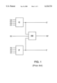
- a portion of an XC4000-Series CLE implementing a 5-input function generator is shown in FIG. 1.
- the outputs F' and G' of the two function generators F and G can be optionally combined with a third signal H1 in a third function generator 3H to form output 3H'.
- the 3H function generator can implement any function of the three inputs (256 functions), including a 2-to-1 multiplexer that can be used when a 5-input function is desired.
- function generators F and G share the same four inputs (F1/G1, F2/G2, F3/G3, F4/G4) and function generator 3H is programmed to function as a 2-to-1 multiplexer
- output 3H' can represent any function of up to five inputs (F1/G1, F2/G2, F3/G3, F4/G4, H1).
- output 3H' can represent some functions of up to nine inputs (F1, F2, F3, F4, G1, G2, G3, G4, H1).
- Function generator 3H can be replaced by a 2-to-1 multiplexer, with signal H1 selecting between outputs F' and G', as disclosed in U.S. Pat. No. 5,349,250 entitled "Logic Structure and Circuit for Fast Carry" by Bernard J. New, which is incorporated herein by reference.
- Replacing the function generator of FIG. 1 with a 2-to-1 multiplexer reduces the number of supported functions with up to nine inputs, but still provides any function of up to five inputs and reduces the silicon area required to implement a five-input-function generator.
- An FPGA using two 4-input function generators and a 2-to-1 multiplexer to implement a five input function generator is the XC5200TM family of products from Xilinx, Inc.
- the XC5200 CLE is described in pages 4-188 through 4-190 of the Xilinx 1996 Data Book entitled “The Programmable Logic Data Book", available from Xilinx, Inc., 2100 Logic Drive, San Jose, Calif. 95124, which are incorporated herein by reference.
- a CLE capable of generating 6-input functions is described as implemented in the ORCATM OR2C FPGAs from Lucent Technologies Inc. ("ORCA” is a trademark of Lucent Technologies Inc.) This CLE is described in pages 2-9 through 2-20 of the Lucent Technologies October 1996 Data Book entitled “Field-Programmable Gate Arrays", available from Microelectronics Group, Lucent Technologies Inc., 555 Union Boulevard, Room 30L-15P-BA, Allentown, Pa. 18103, which are incorporated herein by reference.
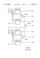
- a portion of an ORCA OR2C CLE implementing a 6-input function generator is shown here in FIG. 2.
- the CLE of FIG. 2 comprises four 4-input function generators QLUT0, QLUT1, QLUT2, QLUT3.
- Function generator QLUT0 has four inputs B0, B1, B2, B3 and function generator QLUT1 has four inputs B1, B2, B3, B4.
- Outputs QL0 and QL1 of function generators QLUT0 and QLUT1, respectively, can be selected between in 2-to-1 multiplexer MUX0 with CLE input signal B4 acting as a select line to form output M0.
- Multiplexer MUX0 therefore can provide functions of five input signals B0, B1, B2, B3, B4.
- function generator QLUT2 has four inputs A0, A1, A2, A3 and function generator QLUT3 has four inputs A1, A2, A3, A4.
- Outputs QL2 and QL3 of function generators QLUT2 and QLUT3, respectively, can be optionally combined in 2-to-1 multiplexer MUX3 with CLE input signal A4 acting as a select line to form output M3.
- Multiplexer MUX3 therefore can provide functions of five input signals A0, A1, A2, A3, A4.
- Multiplexer outputs M0 and M3 can optionally be combined in 2-to-1 multiplexer MUX6 with CLE input signal C0 acting as a select line to form output M1.
- multiplexer output M1 can represent functions of up to six inputs (A0/B0, A1/B1, A2/B2, A3/B3, A4/B4, C0).
- One advantage of including four function generators in a single CLE is the ability to implement circuits requiring three or four function generators, such as 6-input functions, in a single CLE, thereby improving the performance of the circuit. (Connections between CLE outputs and inputs are typically slower than internal connections within a single CLE.)
- one disadvantage is that the resulting software model for the CLE is more complicated than the software model for a smaller, simpler CLE.
- FPGA mapping, placing, routing, and delay estimation software tools require a CLE software model in order to implement a user's design. The more complicated the CLE software model, the more complicated it becomes to write the mapping, placing, routing, and delay estimation software, and the longer the software takes to run. Therefore, it is desirable to increase the number of function generators in a CLE without increasing the complexity of the software model.
- the amount of logic that can be placed in an FPGA is often limited by the amount of interconnect available, particularly in high-density designs (i.e., designs using a high percentage of the available logic blocks). Adding enough interconnect lines to support high-density designs allows a larger percentage of the available logic blocks to be used, but is costly in terms of silicon area because of the silicon required to programmably interconnect the lines. The silicon area for the extra interconnect lines is wasted for designs that do not require the extra interconnect lines. It is therefore desirable to minimize the number of required interconnect lines, rather than adding additional lines for high-density designs.
- the invention provides a Configurable Logic Element (CLE) preferably included in each of an array of identical tiles.
- a CLE according to the invention has four 4-input function generators. The outputs of first and second function generators are combined with a fifth independent input in a five-input-function multiplexer or function generator to produce an output that can be any function of five inputs. Additionally, the multiplexer or function generator can provide some functions of up to nine inputs, since none of the inputs are shared.
- One 6-input function that is particularly useful is a 4-to-1 multiplexer, which is a function frequently used in FPGA customer designs.
- the outputs of the third and fourth function generators are similarly combined.
- the outputs of the two five-input-function multiplexers or function generators are then combined with a sixth independent input in a first six-input-function multiplexer or function generator, and with a different sixth independent input in a second six-input-function multiplexer or function generator.
- the two six-input-function multiplexers or function generators therefore produce two outputs.
- One of the outputs can be any function of six inputs; the other output can be a related function of six inputs, where five inputs and two five-input-function multiplexers or function generators are shared between the two 6-input functions.
- One 11-input function that is particularly useful is an 8-to-1 multiplexer, which is a function frequently used in FPGA customer designs.
- the CLE of the invention is believed to be the first CLE able to generate an 8-to-1 multiplexer using only four 4-input function generators.
- the sixth input is also shared, the two 6-input functions are the same, and the same output signal appears at two exit points on the CLE.
- One method of minimizing the number of required interconnect lines in an FPGA is to provide additional exit points for CLE outputs.
- an output signal can use either exit point, and therefore has a wider choice of interconnect paths than when restricted to one exit point. It is also easier for the software to route the signal, and fewer of the available interconnect lines need be used.
- multiple exit points for a six-input-function output are provided.
- multiple entry points for CLE input signals improve routing flexibility. Since either of two six-input function generators can be used, each having one input independent of the other, logic can be placed in the six-input function generator having the most desirable input connection.
- the CLE is organized into two similar portions called “slices", each slice comprising two function generators, one five-input-function multiplexer, and one six-input-function multiplexer.
- the two slices are symmetric, and in one embodiment are laid out as mirror images of each other. Therefore, a software model for a single slice can be used by the FPGA mapping, placing, routing, and delay estimation software, resulting in a much simpler model than would be required to model the entire CLE. A simpler model decreases software runtime and simplifies the software development process. Additionally, using a similar layout for the two slices results in approximately equal delays between corresponding nodes in the two slices of the CLE and also provides a considerable saving to the FPGA vendor of time and money during the design cycle.
- the second six-input-function multiplexer provides several benefits while using little or no additional silicon area.
- either the five-input-function multiplexers, the six-input-function multiplexers, or both have additional inputs, thereby further increasing the number of functions that can be implemented in the CLE.
- the number of functions supported by the CLE is increased by using 3-input function generators instead of the five-input-function multiplexers, the six-input-function multiplexers, or both.
- FIG. 1 shows a portion of a prior art CLE that can evaluate 5-input functions.
- FIG. 2 shows a portion of a prior art CLE that can evaluate 6-input functions.
- FIG. 3 shows the function generators and multiplexers for a single CLE according to a first embodiment of the invention.
- FIGS. 4A and 4B show the internal logic for one CLE according to a second embodiment of the invention. To view the entire CLE, FIGS. 4A and 4B must be viewed together as shown in the key at the top of FIG. 4A.
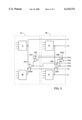
- FIG. 3 shows a simplified block diagram of a portion of a first CLE according to the invention. Included in FIG. 3 are four 4-input function generators F, G, H, J.
- the outputs of function generators F and G (F' and G', respectively) are combined with a fifth independent input BFF in five-input-function multiplexer F5B to produce output F5B', which can be any function of five inputs, or some functions of up to nine inputs.
- the outputs of function generators H and J (H' and J', respectively) are combined with a fifth independent input BHH in five-input-function multiplexer F5A to produce output F5A', which can be any function of five inputs, or some functions of up to nine inputs.
- the outputs F5A' and F5B' of five-input-function multiplexers F5A and F5B are combined with a sixth independent input BGG in a first six-input-function multiplexer F6B, and with a different sixth independent input BJJ in a second six-input-function multiplexer F6A.
- the two six-input-function multiplexers F6A and F6B therefore produce two outputs F6A' and F6B', respectively.
- One of outputs F6A' and F6B' can be any function of six inputs; the other output can be any function of six inputs provided that five inputs are shared between the two 6-input functions.
- the CLE of FIG. 3 can be viewed as two slices SA, SB.
- Each slice SA, SB comprises two 4-input function generators (H and J, F and G, respectively), one five-input-function multiplexer (F5A, F5B, respectively), and one six-input-function multiplexer (F6A, F6B, respectively).
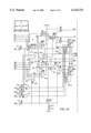
- FIGS. 4A and 4B A second CLE in accordance with the invention is shown in FIGS. 4A and 4B.
- the CLE is implemented in two slices.
- FIGS. 4A and 4B each showing one slice, must be viewed together as shown in the key at the top of FIG. 4A.
- Programmable (configurable) bits controlling the function of the CLE are shown as small boxes containing an "x".
- the CLE of FIGS. 4A and 4B includes four function generators: F and G in FIG. 4B, and H and J in FIG. 4A.
- Function generator F has four inputs F1, F2, F3, F4;
- function generator G has four inputs G1, G2, G3, G4;
- function generator H has four inputs H1, H2, H3, H4;
- function generator J has four inputs J1, J2, J3, J4.
- Each of function generators F, G, H, J also has a data-in input DI and an output O.
- each function generator F, G has a write strobe WS input WSF, WSG, respectively, generated in write strobe generator WB from clock input signal CK0 optionally inverted by multiplexer 69B, set/reset input signal SR0 optionally inverted by multiplexer 60B, and input signal BF optionally inverted by multiplexer VF.
- Each function generator H, J has a write strobe WS input WSH, WSJ, respectively, generated in write strobe generator WA from clock input signal CK1 optionally inverted by multiplexer 69A, set/reset input signal SR1 optionally inverted by multiplexer 60B, and input signal BH optionally inverted by multiplexer VH.
- Function generators F, G, H, J of FIGS. 4A and 4B preferably include novel features described by Bauer in U.S. Pat. No. 5,889,413 entitled “Lookup Tables Which Double as Shift Registers", which is incorporated herein by reference. Briefly, these function generators have the ability to operate as shift registers as well as small RAMs and lookup tables.
- Write strobe signal WS controls the shifting function and the RAM write cycle. (In one embodiment, write strobe signal WS is implemented as two separate control signals, as described by Bauer.)
- Data-in port DI carries a data signal (in this embodiment derived from input signals BF, BH, BG, BJ) for writing to an addressed memory cell.
- the shift register data input signal is taken from BF, BG, BH, BJ, respectively.
- Write strobe generators WB, WA generate write strobe signals WSF and WSG, WSH and WSJ, respectively.
- the use of function generators as RAM is described in pages 4-11 through 4-23 of the Xilinx 1996 Data Book entitled "The Programmable Logic Data Book", available from Xilinx, Inc., 2100 Logic Drive, San Jose, Calif. 95124, which are incorporated herein by reference.
- the function generator of this embodiment can therefore be configured as a look-up table, a shift register, a 16 ⁇ 1 RAM, half of a 16 ⁇ 1 dual-ported RAM (when the two function generators in a slice are paired together), half of a 16 ⁇ 2 RAM, or half of a 32 ⁇ 1 RAM (when the two function generators in a slice are paired together). Not all combinations of function generator configurations are supported in a single slice. The supported combinations are detailed below.
- write strobe signals WSF and WSG are controlled by write strobe generator WB.
- a High (logic 1) pulse on function generator input WS causes a write to occur to the function generator look-up table, to either the first memory cell of the look-up table (if configured as a shift register) or to an addressed cell (if configured as a RAM).
- Write strobe generator WB functions as follows in the supported combinations of function generator configurations: a) when function generators F and G are both configured as look-up tables, write strobe signals WSF and WSG are held Low (logic 0); b) when function generator G is configured as a 16 ⁇ 1 RAM or shift register and function generator F is configured as a look-up table, write strobe signal WSF remains Low while write strobe signal WSG pulses High when SR0 is active (Low or High, depending on whether multiplexer 60B is inverting or not) and CK0 makes the proper transition (falling or rising, depending on whether multiplexer 69B is inverting CK0 or not); c) when function generators F and G are configured as a dual-ported 16 ⁇ 1 RAM, a 16 ⁇ 2 RAM, or a pair of shift registers, write strobe signals WSF and WSG pulse High together when SR0 is active and CK0 makes the proper transition; d) when function generators F and G are configured as a single 32
- the generated High pulse occurs on write strobe signal WSF if multiplexer VF is non-inverting and input signal BF is High or if multiplexer VF is inverting and input signal BF is low, otherwise the High pulse occurs on write strobe signal WSG.
- SR0 acts as a write enable and CK0 acts as a clock to a synchronous RAM or shift register, while BF serves as a fifth address bit when the two function generators in a slice are configured as a 32-bit RAM.
- Write strobe signals WSH and WSJ are generated by write strobe generator WA and controlled by input signals SR1, CK1, and BH, in a corresponding fashion.
- AND gates 61F, 61G, 61H, 61J and multiplexers 81F, 81G, 81H, 81J, CF, CG, CH, CJ implement multiplier and carry logic functions as described in commonly assigned, co-pending U.S. patent application Ser. No. 08/786,818 entitled "Configurable Logic Block with AND Gate for Efficient Multiplication in FPGAs" by Chapman et al, which is referenced above.
- each of multiplexers 81F, 81G, 81H, 81J has separate programmable memory cells that determine the multiplexer output.
- the two multiplexers in each slice (81F and 81G, 81H and 81J) share memory cells and therefore have the same programmed functionality.
- each slice has a separate carry chain.
- One carry chain is from input signal CIN0 to output signal COUT0 and incorporates the outputs of function generators F and G.
- the other carry chain is from input signal CIN1 to output signal COUT1 and incorporates the outputs of function generators H and J.
- the two carry chains are implemented as described in U.S. Pat. No. 5,629,886 entitled "Method and Structure for Providing Fast Propagation of a Carry Signal in a Field Programmable Gate Array" by Bernard J. New, which is incorporated herein by reference.
- Each slice further includes five-input-function multiplexer F5A, F5B and six-input-function multiplexer F6A, F6B.
- multiplexer F6A receives an input signal on west-going line F5W from the output of multiplexer F5B in FIG. 4B.
- six-input-function multiplexer F6B receives an input signal on east-going line F5E from the output of multiplexer F5A in FIG. 4A.
- Multiplexer F6A receives a second input signal from multiplexer F5A
- multiplexer F6B receives a second input signal from multiplexer F5B.
- Multiplexer F5A receives inputs from outputs O of function generators H and J.
- Multiplexer F5B receives inputs from outputs O of function generators F and G.
- the CLE of this embodiment receives four extra control signals on lines BF, BH, BG, and BJ. These lines can be programmably inverted using multiplexers VF, VH, VG, and VJ, respectively, and control several useful functions.
- the five-input function multiplexers F5A, F5B are controlled by lines BH, BF, respectively.
- the six-input function multiplexers F6A, F6B are controlled by lines BJ, BG, respectively.
- a user can form a four-input multiplexer using multiplexer F5A and the outputs of function generators H and J, with function generators H and J each configured as a two-input multiplexer.
- a four-input multiplexer can be formed using multiplexer F5B and the outputs of function generators F and G.
- a user can form an eight-input multiplexer using either multiplexer F6A or multiplexer F6B receiving inputs from both multiplexers F5A and F5B, each of which is receiving outputs from its respective function generators.
- multiplexer F5A the memory cells in function generators H and J can operate as a 32-bit RAM.
- multiplexer F5B the memory cells in function generators F and G can operate as a 32-bit RAM.
- Lines BF, BH, BG, BJ serve as multiplexer control lines or RAM address lines, in addition to other functions as later described.
- Registers RX, RY, RZ, RV generate outputs XQ, YQ, ZQ, VQ, respectively.
- Clock inputs to registers RX, RY, RZ, RV are designated by open triangles with apexes pointing into these registers.
- Clock enable inputs CE can be disabled using AND-gates 62A, 62B. (AND-gates 62A, 62B are controlled by a programmable memory cell that provides one of the inputs to each AND-gate.)
- Registers RX, RY, RZ, RV can be set or reset either synchronously or asynchronously through set port S or reset port R.
- Set/reset input signals SR0, SR1 are controlled by multiplexers 60A, 60B and AND-gates 67A, 67B. Inputs SR0, SR1 (if enabled by AND-gates 67A, 67B) can set or reset the registers.
- Set/reset control units R81B, R82B, R81A, R82A are programmably controlled to either set or reset registers RX, RY, RZ, RV, respectively.
- Registers RX, RY, RZ, RV can also be configured as latches, the choice being made by a programmable memory cell shared between the two registers in each slice.
- XOR gates SF, SG, SH, SJ generate the sum portion of an addition or multiplication, as described in U.S. Pat. No. 5,889,413 entitled "Lookup Tables Which Double as Shift Registers", which is referenced above.
- Multiplexers MF, MG, MH, MJ select between signals to place onto output lines X, Y, Z, V, respectively.
- Multiplexers MF and MH select between the related function generator output signal, sum output signal, and five-input function multiplexer output signal.
- Multiplexers MG and MJ select between the related function generator output signal, sum output signal, and six-input function multiplexer output signal.
- the function generator F, G, H, J output signal is selected when a logical function of up to four inputs is chosen.
- the five-input function multiplexer F5A, F5B output signal is selected when one of a limited set of nine-input functions is chosen, including any logical function of five inputs, a 4-to-1 multiplexer, and any other function that can be implemented as two four-input functions feeding a 2-to-1 multiplexer.
- the six-input function multiplexer F6A, F6B output signal is selected when one of a limited set of 18-input functions is chosen, including any logical function of six inputs, an 8-to-1 multiplexer, and any other function that can be implemented as the output of two five-input function multiplexers F5A, F5B feeding a 2-to-1 multiplexer.
- the sum output signal of XOR gates SF, SG, SH, SJ is selected when an appropriate arithmetic operation such as addition, subtraction or multiplication is implemented.
- Multiplexers OF, OG, OH, OJ allow the carry chain to bypass the related function generator. Multiplexers OF, OG, OH, OJ select whether the respective carry multiplexer CF, CG, CH, CJ is controlled by the function generator output signal O or whether the carry chain bypasses the function generator by propagating the carry-in signal to the next stage along the carry chain. Multiplexers CA, CB allow additional access onto their respective carry chains by selecting either a carry-in signal CIN0, CIN1 (buffered in this embodiment by inverters I121B and I122B, I121A and I122A, respectively) or an input signal BF, BH as the starting point for the carry chain in the CLE.
- Multiplexers DF, DH select a signal to be loaded into related registers RX, RZ either from the outputs of multiplexers MF, MH, or from input signals BF, BH, respectively.
- Multiplexers DG, DJ select a signal to be loaded into related registers RY, RV either from the outputs of multiplexers MG, MJ, or from input signal lines BG, BJ, respectively.
- Multiplexers BB, BA are bypass multiplexers that can apply carry-out signals COUT0, COUT1 to output lines YB, VB, or can forward input signals BG, BJ to output lines YB, VB to route a signal generated on one side of the CLE to a destination on the other side of the CLE.
- AND-gates BRB, BRA allow input signals BG, BJ to serve as set/reset signals to registers RX, RY, RZ, RV, or alternatively allows input signals BG, BJ to be decoupled from registers RX, RY, RZ, RV so that input signals BG, BJ can be used for other purposes, such as controlling multiplexers F6B, F6A or providing a DI signal to function generators G, J, without setting or resetting the registers.
- a logic 0 in the memory cells controlling AND-gates BRB, BRA decouples lines BG, BJ from set/reset control units R81B, R82B, R81A, R82A; while a logic 1 in the associated memory cell enables AND gates BRB, BRA to use the signals on BG, BJ to set or reset registers RX, RY, RZ, RV as determined by set/reset control units R81B, R82B, R81A, R82A.
- the duplicated six-input-function multiplexer or function generator of the present invention offers the benefits of: 1) optionally implementing two different 6-input functions having five shared inputs and two shared 5-input multiplexers or function generators; 2) implementing an 8-to-1 multiplexer using only four 4-input function generators; 3) optionally implementing only one 6-input function but making the output thereof available at either of two exit points on an FPGA tile boundary, thereby reducing the number of required interconnect lines; 4) optionally selecting the six-input function multiplexer or function generator with the most advantageously placed unshared input; 5) a much simpler software model, with corresponding software speed and ease of software development; and 6) approximately equal delays between corresponding nodes in the two slices of the CLE, further simplifying FPGA mapping, placing, routing, and delay estimation software.
- the present invention provides a new and useful method of generating 6-input functions in an FPGA CLE, and further provides a new and useful method of implementing an 8-to-1 multiplexer using only four
Abstract
The invention provides a Configurable Logic Element (CLE) preferably included in each of an array of identical tiles. A CLE according to the invention has four function generators. The outputs of two function generators are combined with a fifth independent input in a five-input-function multiplexer or function generator to produce an output that can be any function of five inputs, or some functions of up to nine inputs. The outputs of the other two function generators are similarly combined. The outputs of the two five-input-function multiplexers or function generators are then combined with a sixth independent input in a six-input-function multiplexer or function generator. The six-input-function multiplexer or function generator therefore produces an output that can be any function of up to six inputs. Some functions of up to nineteen inputs can also be generated in a single CLE.
Description
This application is a divisional application of commonly assigned co-pending U.S. Pat. No. 6,051,992, invented by Steven P. Young, Shekhar Bapat, Kamal Chaudhary, Trevor J. Bauer, and Roman Iwanczuk entitled "CONFIGURABLE LOGIC ELEMENT WITH ABILITY TO EVALUATE FIVE AND SIX INPUT FUNCTIONS" filed Apr. 1, 1999 and issued Apr. 18, 2000, which is a divisional application of commonly assigned U.S. Pat. No. 5,920,202, invented by Steven P. Young, Shekhar Bapat, Kamal Chaudhary, Trevor J. Bauer, and Roman Iwanczuk entitled "CONFIGURABLE LOGIC ELEMENT WITH ABILITY TO EVALUATE FIVE AND SIX INPUT FUNCTIONS", filed Apr. 4, 1997 and issued Jul. 6, 1999, which is a continuation-in-part of commonly assigned U.S. Pat. No. 5,914,616 invented by Steven P. Young, Kamal Chaudhary, and Trevor J. Bauer entitled "FPGA REPEATABLE INTERCONNECT STRUCTURE WITH HIERARCHICAL INTERCONNECT LINES" and filed Feb. 26, 1997, all of which are incorporated herein by reference.
This application further relates to the following commonly assigned co-pending U.S. patent application Ser. No. 08/786,818 invented by Kenneth D. Chapman and Steven P. Young, entitled "CONFIGURABLE LOGIC BLOCK WITH AND GATE FOR EFFICIENT
MULTIPLICATION IN FPGAs" and filed Jan. 21, 1997, which is incorporated herein by reference.
1. Field of the Invention
The invention relates to programmable integrated circuit devices, more particularly to a Configurable Logic Element (CLE) in a field programmable logic device.
2. Description of the Background Art
Field Programmable Gate Arrays (FPGAs) typically include an array of tiles. Each tile includes a Configurable Logic Element (CLE) connectable to CLEs in other tiles through programmable interconnect lines. The interconnect lines typically provide for connecting each CLE to each other CLE.
CLEs typically include combinatorial function generators, which are often implemented as 4-input lookup tables.
Some CLEs can also implement any 5-input function by selecting between the outputs of two 4-input function generators with another CLE input. One such CLE, implemented in the Xilinx XC4000-Series FPGAs, is described in pages 4-11 through 4-23 of the Xilinx 1996 Data Book entitled "The Programmable Logic Data Book", available from Xilinx, Inc., 2100 Logic Drive, San Jose, Calif. 95124, which are incorporated herein by reference. (Xilinx, Inc., owner of the copyright, has no objection to copying these and other pages referenced herein but otherwise reserves all copyright rights whatsoever.) A portion of an XC4000-Series CLE implementing a 5-input function generator is shown in FIG. 1. The outputs F' and G' of the two function generators F and G can be optionally combined with a third signal H1 in a third function generator 3H to form output 3H'. The 3H function generator can implement any function of the three inputs (256 functions), including a 2-to-1 multiplexer that can be used when a 5-input function is desired. When function generators F and G share the same four inputs (F1/G1, F2/G2, F3/G3, F4/G4) and function generator 3H is programmed to function as a 2-to-1 multiplexer, output 3H' can represent any function of up to five inputs (F1/G1, F2/G2, F3/G3, F4/G4, H1). When the inputs to function generators F and G are independent, output 3H' can represent some functions of up to nine inputs (F1, F2, F3, F4, G1, G2, G3, G4, H1).
Function generator 3H can be replaced by a 2-to-1 multiplexer, with signal H1 selecting between outputs F' and G', as disclosed in U.S. Pat. No. 5,349,250 entitled "Logic Structure and Circuit for Fast Carry" by Bernard J. New, which is incorporated herein by reference. Replacing the function generator of FIG. 1 with a 2-to-1 multiplexer reduces the number of supported functions with up to nine inputs, but still provides any function of up to five inputs and reduces the silicon area required to implement a five-input-function generator. An FPGA using two 4-input function generators and a 2-to-1 multiplexer to implement a five input function generator is the XC5200™ family of products from Xilinx, Inc. The XC5200 CLE is described in pages 4-188 through 4-190 of the Xilinx 1996 Data Book entitled "The Programmable Logic Data Book", available from Xilinx, Inc., 2100 Logic Drive, San Jose, Calif. 95124, which are incorporated herein by reference.
A CLE capable of generating 6-input functions is described as implemented in the ORCA™ OR2C FPGAs from Lucent Technologies Inc. ("ORCA" is a trademark of Lucent Technologies Inc.) This CLE is described in pages 2-9 through 2-20 of the Lucent Technologies October 1996 Data Book entitled "Field-Programmable Gate Arrays", available from Microelectronics Group, Lucent Technologies Inc., 555 Union Boulevard, Room 30L-15P-BA, Allentown, Pa. 18103, which are incorporated herein by reference. A portion of an ORCA OR2C CLE implementing a 6-input function generator is shown here in FIG. 2. The CLE of FIG. 2 comprises four 4-input function generators QLUT0, QLUT1, QLUT2, QLUT3. Function generator QLUT0 has four inputs B0, B1, B2, B3 and function generator QLUT1 has four inputs B1, B2, B3, B4. Outputs QL0 and QL1 of function generators QLUT0 and QLUT1, respectively, can be selected between in 2-to-1 multiplexer MUX0 with CLE input signal B4 acting as a select line to form output M0. Multiplexer MUX0 therefore can provide functions of five input signals B0, B1, B2, B3, B4. Similarly, function generator QLUT2 has four inputs A0, A1, A2, A3 and function generator QLUT3 has four inputs A1, A2, A3, A4. Outputs QL2 and QL3 of function generators QLUT2 and QLUT3, respectively, can be optionally combined in 2-to-1 multiplexer MUX3 with CLE input signal A4 acting as a select line to form output M3. Multiplexer MUX3 therefore can provide functions of five input signals A0, A1, A2, A3, A4. Multiplexer outputs M0 and M3 can optionally be combined in 2-to-1 multiplexer MUX6 with CLE input signal C0 acting as a select line to form output M1. When input signals A0, A1, A2, A3, A4 are shared with input signals B0, B1, B2, B3, B4, respectively, multiplexer output M1 can represent functions of up to six inputs (A0/B0, A1/B1, A2/B2, A3/B3, A4/B4, C0).
One advantage of including four function generators in a single CLE is the ability to implement circuits requiring three or four function generators, such as 6-input functions, in a single CLE, thereby improving the performance of the circuit. (Connections between CLE outputs and inputs are typically slower than internal connections within a single CLE.) However, one disadvantage is that the resulting software model for the CLE is more complicated than the software model for a smaller, simpler CLE. FPGA mapping, placing, routing, and delay estimation software tools require a CLE software model in order to implement a user's design. The more complicated the CLE software model, the more complicated it becomes to write the mapping, placing, routing, and delay estimation software, and the longer the software takes to run. Therefore, it is desirable to increase the number of function generators in a CLE without increasing the complexity of the software model.
Additionally, the amount of logic that can be placed in an FPGA is often limited by the amount of interconnect available, particularly in high-density designs (i.e., designs using a high percentage of the available logic blocks). Adding enough interconnect lines to support high-density designs allows a larger percentage of the available logic blocks to be used, but is costly in terms of silicon area because of the silicon required to programmably interconnect the lines. The silicon area for the extra interconnect lines is wasted for designs that do not require the extra interconnect lines. It is therefore desirable to minimize the number of required interconnect lines, rather than adding additional lines for high-density designs.
The invention provides a Configurable Logic Element (CLE) preferably included in each of an array of identical tiles. A CLE according to the invention has four 4-input function generators. The outputs of first and second function generators are combined with a fifth independent input in a five-input-function multiplexer or function generator to produce an output that can be any function of five inputs. Additionally, the multiplexer or function generator can provide some functions of up to nine inputs, since none of the inputs are shared. One 6-input function that is particularly useful is a 4-to-1 multiplexer, which is a function frequently used in FPGA customer designs. The outputs of the third and fourth function generators are similarly combined.
The outputs of the two five-input-function multiplexers or function generators are then combined with a sixth independent input in a first six-input-function multiplexer or function generator, and with a different sixth independent input in a second six-input-function multiplexer or function generator. The two six-input-function multiplexers or function generators therefore produce two outputs. One of the outputs can be any function of six inputs; the other output can be a related function of six inputs, where five inputs and two five-input-function multiplexers or function generators are shared between the two 6-input functions. Some functions of up to nineteen inputs can also be generated in a single CLE, since none of the inputs are shared. One 11-input function that is particularly useful is an 8-to-1 multiplexer, which is a function frequently used in FPGA customer designs. The CLE of the invention is believed to be the first CLE able to generate an 8-to-1 multiplexer using only four 4-input function generators. When the sixth input is also shared, the two 6-input functions are the same, and the same output signal appears at two exit points on the CLE.
One method of minimizing the number of required interconnect lines in an FPGA is to provide additional exit points for CLE outputs. When two exit points are provided, an output signal can use either exit point, and therefore has a wider choice of interconnect paths than when restricted to one exit point. It is also easier for the software to route the signal, and fewer of the available interconnect lines need be used. In a CLE according to the invention, multiple exit points for a six-input-function output are provided.
Similarly, multiple entry points for CLE input signals improve routing flexibility. Since either of two six-input function generators can be used, each having one input independent of the other, logic can be placed in the six-input function generator having the most desirable input connection.
In one embodiment, the CLE is organized into two similar portions called "slices", each slice comprising two function generators, one five-input-function multiplexer, and one six-input-function multiplexer. The two slices are symmetric, and in one embodiment are laid out as mirror images of each other. Therefore, a software model for a single slice can be used by the FPGA mapping, placing, routing, and delay estimation software, resulting in a much simpler model than would be required to model the entire CLE. A simpler model decreases software runtime and simplifies the software development process. Additionally, using a similar layout for the two slices results in approximately equal delays between corresponding nodes in the two slices of the CLE and also provides a considerable saving to the FPGA vendor of time and money during the design cycle. Further, when the same layout is used for both slices the CLE is the same size with two six-input-function multiplexers as it would be if only one six-input-function multiplexer were provided. Therefore, in this embodiment, the second six-input-function multiplexer provides several benefits while using little or no additional silicon area.
In other embodiments, either the five-input-function multiplexers, the six-input-function multiplexers, or both, have additional inputs, thereby further increasing the number of functions that can be implemented in the CLE. In other embodiments, the number of functions supported by the CLE is increased by using 3-input function generators instead of the five-input-function multiplexers, the six-input-function multiplexers, or both.
FIG. 1 shows a portion of a prior art CLE that can evaluate 5-input functions.
FIG. 2 shows a portion of a prior art CLE that can evaluate 6-input functions.
FIG. 3 shows the function generators and multiplexers for a single CLE according to a first embodiment of the invention.
FIGS. 4A and 4B show the internal logic for one CLE according to a second embodiment of the invention. To view the entire CLE, FIGS. 4A and 4B must be viewed together as shown in the key at the top of FIG. 4A.
A First CLE According to the Invention
FIG. 3 shows a simplified block diagram of a portion of a first CLE according to the invention. Included in FIG. 3 are four 4-input function generators F, G, H, J. The outputs of function generators F and G (F' and G', respectively) are combined with a fifth independent input BFF in five-input-function multiplexer F5B to produce output F5B', which can be any function of five inputs, or some functions of up to nine inputs. The outputs of function generators H and J (H' and J', respectively) are combined with a fifth independent input BHH in five-input-function multiplexer F5A to produce output F5A', which can be any function of five inputs, or some functions of up to nine inputs. The outputs F5A' and F5B' of five-input-function multiplexers F5A and F5B are combined with a sixth independent input BGG in a first six-input-function multiplexer F6B, and with a different sixth independent input BJJ in a second six-input-function multiplexer F6A. The two six-input-function multiplexers F6A and F6B therefore produce two outputs F6A' and F6B', respectively. One of outputs F6A' and F6B' can be any function of six inputs; the other output can be any function of six inputs provided that five inputs are shared between the two 6-input functions. Some functions of up to nineteen inputs can also be generated in a single CLE.
The CLE of FIG. 3 can be viewed as two slices SA, SB. Each slice SA, SB comprises two 4-input function generators (H and J, F and G, respectively), one five-input-function multiplexer (F5A, F5B, respectively), and one six-input-function multiplexer (F6A, F6B, respectively).
A Second CLE According to the Invention
A second CLE in accordance with the invention is shown in FIGS. 4A and 4B. In this embodiment, the CLE is implemented in two slices. To view the entire CLE, FIGS. 4A and 4B, each showing one slice, must be viewed together as shown in the key at the top of FIG. 4A. Programmable (configurable) bits controlling the function of the CLE are shown as small boxes containing an "x".
The details of one function generator compatible with the CLE of the invention are shown and described in commonly assigned, co-pending U.S. application Ser. No. 08/786,818 entitled "Configurable Logic Block with AND Gate for Efficient Multiplication in FPGAs" by Chapman et al, which is referenced above.
The CLE of FIGS. 4A and 4B includes four function generators: F and G in FIG. 4B, and H and J in FIG. 4A. Function generator F has four inputs F1, F2, F3, F4; function generator G has four inputs G1, G2, G3, G4; function generator H has four inputs H1, H2, H3, H4; and function generator J has four inputs J1, J2, J3, J4. Each of function generators F, G, H, J also has a data-in input DI and an output O. In addition, each function generator F, G has a write strobe WS input WSF, WSG, respectively, generated in write strobe generator WB from clock input signal CK0 optionally inverted by multiplexer 69B, set/reset input signal SR0 optionally inverted by multiplexer 60B, and input signal BF optionally inverted by multiplexer VF. Each function generator H, J has a write strobe WS input WSH, WSJ, respectively, generated in write strobe generator WA from clock input signal CK1 optionally inverted by multiplexer 69A, set/reset input signal SR1 optionally inverted by multiplexer 60B, and input signal BH optionally inverted by multiplexer VH.
Function generators F, G, H, J of FIGS. 4A and 4B preferably include novel features described by Bauer in U.S. Pat. No. 5,889,413 entitled "Lookup Tables Which Double as Shift Registers", which is incorporated herein by reference. Briefly, these function generators have the ability to operate as shift registers as well as small RAMs and lookup tables. Write strobe signal WS controls the shifting function and the RAM write cycle. (In one embodiment, write strobe signal WS is implemented as two separate control signals, as described by Bauer.) Data-in port DI carries a data signal (in this embodiment derived from input signals BF, BH, BG, BJ) for writing to an addressed memory cell. When function generators F, G, H, J are configured as shift registers as described by Bauer, the shift register data input signal is taken from BF, BG, BH, BJ, respectively. Write strobe generators WB, WA generate write strobe signals WSF and WSG, WSH and WSJ, respectively. Signals WSF, WSG, WSH, WSJ strobe data into their respective function generators during a write cycle when the function generators are configured as RAM, and cause a shift when the function generators are configured as shift registers. The use of function generators as RAM is described in pages 4-11 through 4-23 of the Xilinx 1996 Data Book entitled "The Programmable Logic Data Book", available from Xilinx, Inc., 2100 Logic Drive, San Jose, Calif. 95124, which are incorporated herein by reference.
The function generator of this embodiment can therefore be configured as a look-up table, a shift register, a 16×1 RAM, half of a 16×1 dual-ported RAM (when the two function generators in a slice are paired together), half of a 16×2 RAM, or half of a 32×1 RAM (when the two function generators in a slice are paired together). Not all combinations of function generator configurations are supported in a single slice. The supported combinations are detailed below.
In this embodiment, write strobe signals WSF and WSG are controlled by write strobe generator WB. A High (logic 1) pulse on function generator input WS causes a write to occur to the function generator look-up table, to either the first memory cell of the look-up table (if configured as a shift register) or to an addressed cell (if configured as a RAM). (See U.S. Pat. No. 5,889,413 entitled "Lookup Tables Which Double as Shift Registers", which is referenced above.)
Write strobe generator WB functions as follows in the supported combinations of function generator configurations: a) when function generators F and G are both configured as look-up tables, write strobe signals WSF and WSG are held Low (logic 0); b) when function generator G is configured as a 16×1 RAM or shift register and function generator F is configured as a look-up table, write strobe signal WSF remains Low while write strobe signal WSG pulses High when SR0 is active (Low or High, depending on whether multiplexer 60B is inverting or not) and CK0 makes the proper transition (falling or rising, depending on whether multiplexer 69B is inverting CK0 or not); c) when function generators F and G are configured as a dual-ported 16×1 RAM, a 16×2 RAM, or a pair of shift registers, write strobe signals WSF and WSG pulse High together when SR0 is active and CK0 makes the proper transition; d) when function generators F and G are configured as a single 32×1 RAM, one but not both of write strobe signals WSF and WSG pulses High, when SR0 is active and CK0 makes the proper transition. The generated High pulse occurs on write strobe signal WSF if multiplexer VF is non-inverting and input signal BF is High or if multiplexer VF is inverting and input signal BF is low, otherwise the High pulse occurs on write strobe signal WSG. As can be seen from the above description, SR0 acts as a write enable and CK0 acts as a clock to a synchronous RAM or shift register, while BF serves as a fifth address bit when the two function generators in a slice are configured as a 32-bit RAM.
Write strobe signals WSH and WSJ are generated by write strobe generator WA and controlled by input signals SR1, CK1, and BH, in a corresponding fashion.
AND gates 61F, 61G, 61H, 61J and multiplexers 81F, 81G, 81H, 81J, CF, CG, CH, CJ implement multiplier and carry logic functions as described in commonly assigned, co-pending U.S. patent application Ser. No. 08/786,818 entitled "Configurable Logic Block with AND Gate for Efficient Multiplication in FPGAs" by Chapman et al, which is referenced above. In FIGS. 4A and 4B, each of multiplexers 81F, 81G, 81H, 81J has separate programmable memory cells that determine the multiplexer output. In another embodiment, the two multiplexers in each slice (81F and 81G, 81H and 81J) share memory cells and therefore have the same programmed functionality.
In the embodiment of FIGS. 4A and 4B, each slice has a separate carry chain. One carry chain is from input signal CIN0 to output signal COUT0 and incorporates the outputs of function generators F and G. The other carry chain is from input signal CIN1 to output signal COUT1 and incorporates the outputs of function generators H and J. In one embodiment, the two carry chains are implemented as described in U.S. Pat. No. 5,629,886 entitled "Method and Structure for Providing Fast Propagation of a Carry Signal in a Field Programmable Gate Array" by Bernard J. New, which is incorporated herein by reference.
Each slice further includes five-input-function multiplexer F5A, F5B and six-input-function multiplexer F6A, F6B. In FIG. 4A, multiplexer F6A receives an input signal on west-going line F5W from the output of multiplexer F5B in FIG. 4B. In FIG. 4B, six-input-function multiplexer F6B receives an input signal on east-going line F5E from the output of multiplexer F5A in FIG. 4A. Multiplexer F6A receives a second input signal from multiplexer F5A, and multiplexer F6B receives a second input signal from multiplexer F5B. Multiplexer F5A receives inputs from outputs O of function generators H and J. Multiplexer F5B receives inputs from outputs O of function generators F and G.
The CLE of this embodiment receives four extra control signals on lines BF, BH, BG, and BJ. These lines can be programmably inverted using multiplexers VF, VH, VG, and VJ, respectively, and control several useful functions. The five-input function multiplexers F5A, F5B are controlled by lines BH, BF, respectively. The six-input function multiplexers F6A, F6B are controlled by lines BJ, BG, respectively. A user can form a four-input multiplexer using multiplexer F5A and the outputs of function generators H and J, with function generators H and J each configured as a two-input multiplexer. Similarly, a four-input multiplexer can be formed using multiplexer F5B and the outputs of function generators F and G. A user can form an eight-input multiplexer using either multiplexer F6A or multiplexer F6B receiving inputs from both multiplexers F5A and F5B, each of which is receiving outputs from its respective function generators. Further, with multiplexer F5A, the memory cells in function generators H and J can operate as a 32-bit RAM. With multiplexer F5B, the memory cells in function generators F and G can operate as a 32-bit RAM. Lines BF, BH, BG, BJ serve as multiplexer control lines or RAM address lines, in addition to other functions as later described.
Registers RX, RY, RZ, RV generate outputs XQ, YQ, ZQ, VQ, respectively. Clock inputs to registers RX, RY, RZ, RV are designated by open triangles with apexes pointing into these registers. Clock enable inputs CE can be disabled using AND-gates 62A, 62B. (AND-gates 62A, 62B are controlled by a programmable memory cell that provides one of the inputs to each AND-gate.) Registers RX, RY, RZ, RV can be set or reset either synchronously or asynchronously through set port S or reset port R. (The choice of synchronous or asynchronous is made by a programmable memory cell shared between the two registers in each slice.) Set/reset input signals SR0, SR1 are controlled by multiplexers 60A, 60B and AND-gates 67A, 67B. Inputs SR0, SR1 (if enabled by AND-gates 67A, 67B) can set or reset the registers. Set/reset control units R81B, R82B, R81A, R82A are programmably controlled to either set or reset registers RX, RY, RZ, RV, respectively. Registers RX, RY, RZ, RV can also be configured as latches, the choice being made by a programmable memory cell shared between the two registers in each slice.
XOR gates SF, SG, SH, SJ generate the sum portion of an addition or multiplication, as described in U.S. Pat. No. 5,889,413 entitled "Lookup Tables Which Double as Shift Registers", which is referenced above.
Multiplexers MF, MG, MH, MJ select between signals to place onto output lines X, Y, Z, V, respectively. Multiplexers MF and MH select between the related function generator output signal, sum output signal, and five-input function multiplexer output signal. Multiplexers MG and MJ select between the related function generator output signal, sum output signal, and six-input function multiplexer output signal. The function generator F, G, H, J output signal is selected when a logical function of up to four inputs is chosen. The five-input function multiplexer F5A, F5B output signal is selected when one of a limited set of nine-input functions is chosen, including any logical function of five inputs, a 4-to-1 multiplexer, and any other function that can be implemented as two four-input functions feeding a 2-to-1 multiplexer. The six-input function multiplexer F6A, F6B output signal is selected when one of a limited set of 18-input functions is chosen, including any logical function of six inputs, an 8-to-1 multiplexer, and any other function that can be implemented as the output of two five-input function multiplexers F5A, F5B feeding a 2-to-1 multiplexer. The sum output signal of XOR gates SF, SG, SH, SJ is selected when an appropriate arithmetic operation such as addition, subtraction or multiplication is implemented.
Multiplexers OF, OG, OH, OJ allow the carry chain to bypass the related function generator. Multiplexers OF, OG, OH, OJ select whether the respective carry multiplexer CF, CG, CH, CJ is controlled by the function generator output signal O or whether the carry chain bypasses the function generator by propagating the carry-in signal to the next stage along the carry chain. Multiplexers CA, CB allow additional access onto their respective carry chains by selecting either a carry-in signal CIN0, CIN1 (buffered in this embodiment by inverters I121B and I122B, I121A and I122A, respectively) or an input signal BF, BH as the starting point for the carry chain in the CLE.
Multiplexers DF, DH select a signal to be loaded into related registers RX, RZ either from the outputs of multiplexers MF, MH, or from input signals BF, BH, respectively. Multiplexers DG, DJ select a signal to be loaded into related registers RY, RV either from the outputs of multiplexers MG, MJ, or from input signal lines BG, BJ, respectively.
Multiplexers BB, BA are bypass multiplexers that can apply carry-out signals COUT0, COUT1 to output lines YB, VB, or can forward input signals BG, BJ to output lines YB, VB to route a signal generated on one side of the CLE to a destination on the other side of the CLE.
AND-gates BRB, BRA allow input signals BG, BJ to serve as set/reset signals to registers RX, RY, RZ, RV, or alternatively allows input signals BG, BJ to be decoupled from registers RX, RY, RZ, RV so that input signals BG, BJ can be used for other purposes, such as controlling multiplexers F6B, F6A or providing a DI signal to function generators G, J, without setting or resetting the registers. A logic 0 in the memory cells controlling AND-gates BRB, BRA decouples lines BG, BJ from set/reset control units R81B, R82B, R81A, R82A; while a logic 1 in the associated memory cell enables AND gates BRB, BRA to use the signals on BG, BJ to set or reset registers RX, RY, RZ, RV as determined by set/reset control units R81B, R82B, R81A, R82A.
The duplicated six-input-function multiplexer or function generator of the present invention offers the benefits of: 1) optionally implementing two different 6-input functions having five shared inputs and two shared 5-input multiplexers or function generators; 2) implementing an 8-to-1 multiplexer using only four 4-input function generators; 3) optionally implementing only one 6-input function but making the output thereof available at either of two exit points on an FPGA tile boundary, thereby reducing the number of required interconnect lines; 4) optionally selecting the six-input function multiplexer or function generator with the most advantageously placed unshared input; 5) a much simpler software model, with corresponding software speed and ease of software development; and 6) approximately equal delays between corresponding nodes in the two slices of the CLE, further simplifying FPGA mapping, placing, routing, and delay estimation software. Thus it will be understood that the present invention provides a new and useful method of generating 6-input functions in an FPGA CLE, and further provides a new and useful method of implementing an 8-to-1 multiplexer using only four 4-input function generators.
Those having skill in the relevant arts of the invention will now perceive various modifications and additions which may be made as a result of the disclosure herein of the preferred embodiment. Accordingly, all such modifications and additions are deemed to be within the scope of the invention, which is to be limited only by the appended claims and their equivalents.
Claims (6)
1. A Configurable Logic Element (CLE), comprising:
first, second, third, and fourth function generators, each having a plurality of input signals and an output signal, each of the first, second, third, and fourth function generators being capable of generating any function of the corresponding plurality of input signals, each plurality of input signals comprising the same number of signals;
a first multiplexer selecting at least between the output signals of the first and second function generators, thereby generating a first output signal representing any function of up to M input signals, where M is one more than the number of signals in each plurality of input signals;
a second multiplexer selecting at least between the output signals of the third and fourth function generators, thereby generating a second output signal representing any function of up to M input signals; and
a third multiplexer selecting at least between the first and second output signals, thereby generating a third output signal representing any function of up to M+l input signals.
2. The CLE of claim 1, further comprising a first input signal, and wherein the third multiplexer uses the first input signal to select between the first and second output signals.
3. The CLE of claim 1, wherein M is five.
4. A Configurable Logic Element (CLE), comprising:
first, second, third, and fourth function generators, each having a plurality of input signals and an output signal, each of the first, second, third, and fourth function generators being capable of generating any function of the corresponding plurality of input signals, each plurality of input signals comprising the same number of signals;
a first multiplexer selecting at least between the output signals of the first and second function generators, thereby generating a first output signal representing any function of up to M input signals, where M is one more than the number of signals in each plurality of input signals;
a second multiplexer selecting at least between the output signals of the third and fourth function generators, thereby generating a second output signal representing any function of up to M input signals; and
a fifth function generator having as input signals at least the first and second output signals.
5. The CLE of claim 4, further comprising a first input signal, and wherein the fifth function generator has as input signals at least the first and second output signals and the first input signal.
6. The CLE of claim 4, wherein M is five.
Priority Applications (1)
| Application Number | Priority Date | Filing Date | Title |
|---|---|---|---|
| US09/480,845 US6124731A (en) | 1997-02-26 | 2000-01-10 | Configurable logic element with ability to evaluate wide logic functions |
Applications Claiming Priority (4)
| Application Number | Priority Date | Filing Date | Title |
|---|---|---|---|
| US08/806,997 US5914616A (en) | 1997-02-26 | 1997-02-26 | FPGA repeatable interconnect structure with hierarchical interconnect lines |
| US08/835,088 US5920202A (en) | 1997-02-26 | 1997-04-04 | Configurable logic element with ability to evaluate five and six input functions |
| US09/283,472 US6051992A (en) | 1997-02-26 | 1999-04-01 | Configurable logic element with ability to evaluate five and six input functions |
| US09/480,845 US6124731A (en) | 1997-02-26 | 2000-01-10 | Configurable logic element with ability to evaluate wide logic functions |
Related Parent Applications (1)
| Application Number | Title | Priority Date | Filing Date |
|---|---|---|---|
| US09/283,472 Division US6051992A (en) | 1997-02-26 | 1999-04-01 | Configurable logic element with ability to evaluate five and six input functions |
Publications (1)
| Publication Number | Publication Date |
|---|---|
| US6124731A true US6124731A (en) | 2000-09-26 |
Family
ID=25268546
Family Applications (3)
| Application Number | Title | Priority Date | Filing Date |
|---|---|---|---|
| US08/835,088 Expired - Lifetime US5920202A (en) | 1997-02-26 | 1997-04-04 | Configurable logic element with ability to evaluate five and six input functions |
| US09/283,472 Expired - Lifetime US6051992A (en) | 1997-02-26 | 1999-04-01 | Configurable logic element with ability to evaluate five and six input functions |
| US09/480,845 Expired - Lifetime US6124731A (en) | 1997-02-26 | 2000-01-10 | Configurable logic element with ability to evaluate wide logic functions |
Family Applications Before (2)
| Application Number | Title | Priority Date | Filing Date |
|---|---|---|---|
| US08/835,088 Expired - Lifetime US5920202A (en) | 1997-02-26 | 1997-04-04 | Configurable logic element with ability to evaluate five and six input functions |
| US09/283,472 Expired - Lifetime US6051992A (en) | 1997-02-26 | 1999-04-01 | Configurable logic element with ability to evaluate five and six input functions |
Country Status (2)
| Country | Link |
|---|---|
| US (3) | US5920202A (en) |
| WO (1) | WO1998045947A1 (en) |
Cited By (22)
| Publication number | Priority date | Publication date | Assignee | Title |
|---|---|---|---|---|
| US6222381B1 (en) * | 1999-12-31 | 2001-04-24 | Lisa J. K. Durbeck | Self-configurable parallel processing system made from self-dual code/data processing cells utilizing a non-shifting memory |
| US20030085733A1 (en) * | 2001-10-16 | 2003-05-08 | Pugh Daniel J. | Field programmable gate array core cell with efficient logic packing |
| US20050127944A1 (en) * | 2002-10-24 | 2005-06-16 | Altera Corporation | Versatile logic element and logic array block |
| US7030652B1 (en) | 2004-04-23 | 2006-04-18 | Altera Corporation | LUT-based logic element with support for Shannon decomposition and associated method |
| US20060158218A1 (en) * | 2003-02-19 | 2006-07-20 | Katarzyna Leijten-Nowak | Electronic circuit with array of programmable logic cells |
| US7167022B1 (en) * | 2004-03-25 | 2007-01-23 | Altera Corporation | Omnibus logic element including look up table based logic elements |
| US7196543B1 (en) | 2005-06-14 | 2007-03-27 | Xilinx, Inc. | Integrated circuit having a programmable input structure with optional fanout capability |
| US7202698B1 (en) | 2005-06-14 | 2007-04-10 | Xilinx, Inc. | Integrated circuit having a programmable input structure with bounce capability |
| US20070089082A1 (en) * | 2000-09-02 | 2007-04-19 | Actel Corporation | Freeway routing system for a gate array |
| US7218140B1 (en) | 2005-06-14 | 2007-05-15 | Xilinx, Inc. | Integrated circuit having fast interconnect paths between carry chain multiplexers and lookup tables |
| US7218143B1 (en) * | 2005-06-14 | 2007-05-15 | Xilinx, Inc. | Integrated circuit having fast interconnect paths between memory elements and carry logic |
| US7239173B1 (en) * | 2005-09-07 | 2007-07-03 | Xilinx, Inc. | Programmable memory element with power save mode in a programmable logic device |
| US7253658B1 (en) | 2005-06-14 | 2007-08-07 | Xilinx, Inc. | Integrated circuit providing direct access to multi-directional interconnect lines in a general interconnect structure |
| US7256612B1 (en) * | 2005-06-14 | 2007-08-14 | Xilinx, Inc. | Programmable logic block providing carry chain with programmable initialization values |
| US7265576B1 (en) | 2005-06-14 | 2007-09-04 | Xilinx, Inc. | Programmable lookup table with dual input and output terminals in RAM mode |
| US7274214B1 (en) | 2005-06-14 | 2007-09-25 | Xilinx, Inc. | Efficient tile layout for a programmable logic device |
| US7276934B1 (en) | 2005-06-14 | 2007-10-02 | Xilinx, Inc. | Integrated circuit with programmable routing structure including diagonal interconnect lines |
| US7279929B1 (en) | 2005-06-14 | 2007-10-09 | Xilinx, Inc. | Integrated circuit with programmable routing structure including straight and diagonal interconnect lines |
| US7375552B1 (en) | 2005-06-14 | 2008-05-20 | Xilinx, Inc. | Programmable logic block with dedicated and selectable lookup table outputs coupled to general interconnect structure |
| US20080218208A1 (en) * | 2007-03-09 | 2008-09-11 | Altera Corporation | Programmable logic device having logic array block interconnect lines that can interconnect logic elements in different logic blocks |
| US7508231B2 (en) | 2007-03-09 | 2009-03-24 | Altera Corporation | Programmable logic device having redundancy with logic element granularity |
| US7804719B1 (en) | 2005-06-14 | 2010-09-28 | Xilinx, Inc. | Programmable logic block having reduced output delay during RAM write processes when programmed to function in RAM mode |
Families Citing this family (47)
| Publication number | Priority date | Publication date | Assignee | Title |
|---|---|---|---|---|
| US6288568B1 (en) * | 1996-11-22 | 2001-09-11 | Xilinx, Inc. | FPGA architecture with deep look-up table RAMs |
| US6201410B1 (en) | 1997-02-26 | 2001-03-13 | Xilinx, Inc. | Wide logic gate implemented in an FPGA configurable logic element |
| US5963050A (en) | 1997-02-26 | 1999-10-05 | Xilinx, Inc. | Configurable logic element with fast feedback paths |
| US6097212A (en) | 1997-10-09 | 2000-08-01 | Lattice Semiconductor Corporation | Variable grain architecture for FPGA integrated circuits |
| US6191611B1 (en) * | 1997-10-16 | 2001-02-20 | Altera Corporation | Driver circuitry for programmable logic devices with hierarchical interconnection resources |
| US6211696B1 (en) * | 1998-05-30 | 2001-04-03 | Cypress Semiconductor Corp. | Hybrid product term and look-up table-based programmable logic device with improved speed and area efficiency |
| US6201408B1 (en) | 1998-05-30 | 2001-03-13 | Cypress Semiconductor Corp. | Hybrid product term and look-up table-based programmable logic device with improved speed and area efficiency |
| US6204686B1 (en) * | 1998-12-16 | 2001-03-20 | Vantis Corporation | Methods for configuring FPGA's having variable grain blocks and shared logic for providing symmetric routing of result output to differently-directed and tristateable interconnect resources |
| US6157209A (en) * | 1998-12-18 | 2000-12-05 | Xilinx, Inc. | Loadable up-down counter with asynchronous reset |
| US6407576B1 (en) * | 1999-03-04 | 2002-06-18 | Altera Corporation | Interconnection and input/output resources for programmable logic integrated circuit devices |
| US6359468B1 (en) | 1999-03-04 | 2002-03-19 | Altera Corporation | Programmable logic device with carry look-ahead |
| US6543030B1 (en) * | 1999-05-07 | 2003-04-01 | Koninklijke Philips Electronics N.V. | Computer-implemented conversion of combination-logic module for improving timing characteristics of incorporating integrated circuit design |
| US6633181B1 (en) * | 1999-12-30 | 2003-10-14 | Stretch, Inc. | Multi-scale programmable array |
| US6388466B1 (en) | 2001-04-27 | 2002-05-14 | Xilinx, Inc. | FPGA logic element with variable-length shift register capability |
| US6466052B1 (en) | 2001-05-15 | 2002-10-15 | Xilinx, Inc. | Implementing wide multiplexers in an FPGA using a horizontal chain structure |
| US6943589B2 (en) * | 2001-05-15 | 2005-09-13 | Broadcom Corporation | Combination multiplexer and tristate driver circuit |
| US6995600B2 (en) * | 2001-07-09 | 2006-02-07 | Broadcom Corporation | Fast and wire multiplexing circuits |
| US6556042B1 (en) | 2002-02-20 | 2003-04-29 | Xilinx, Inc. | FPGA with improved structure for implementing large multiplexers |
| AU2003238633A1 (en) * | 2002-07-10 | 2004-02-02 | Koninklijke Philips Electronics N.V. | Electronic circuit with array of programmable logic cells |
| US7028281B1 (en) | 2002-07-12 | 2006-04-11 | Lattice Semiconductor Corporation | FPGA with register-intensive architecture |
| US6798240B1 (en) * | 2003-01-24 | 2004-09-28 | Altera Corporation | Logic circuitry with shared lookup table |
| US7800401B1 (en) | 2003-02-10 | 2010-09-21 | Altera Corporation | Fracturable lookup table and logic element |
| US6943580B2 (en) * | 2003-02-10 | 2005-09-13 | Altera Corporation | Fracturable lookup table and logic element |
| US6888373B2 (en) * | 2003-02-11 | 2005-05-03 | Altera Corporation | Fracturable incomplete look up table for area efficient logic elements |
| US7581081B2 (en) | 2003-03-31 | 2009-08-25 | Stretch, Inc. | Systems and methods for software extensible multi-processing |
| US7613900B2 (en) * | 2003-03-31 | 2009-11-03 | Stretch, Inc. | Systems and methods for selecting input/output configuration in an integrated circuit |
| US8001266B1 (en) | 2003-03-31 | 2011-08-16 | Stretch, Inc. | Configuring a multi-processor system |
| US7000211B2 (en) * | 2003-03-31 | 2006-02-14 | Stretch, Inc. | System and method for efficiently mapping heterogeneous objects onto an array of heterogeneous programmable logic resources |
| US7590829B2 (en) * | 2003-03-31 | 2009-09-15 | Stretch, Inc. | Extension adapter |
| US7373642B2 (en) * | 2003-07-29 | 2008-05-13 | Stretch, Inc. | Defining instruction extensions in a standard programming language |
| US7418575B2 (en) * | 2003-07-29 | 2008-08-26 | Stretch, Inc. | Long instruction word processing with instruction extensions |
| US7185035B1 (en) | 2003-10-23 | 2007-02-27 | Altera Corporation | Arithmetic structures for programmable logic devices |
| US7565388B1 (en) | 2003-11-21 | 2009-07-21 | Altera Corporation | Logic cell supporting addition of three binary words |
| US7164290B2 (en) * | 2004-06-10 | 2007-01-16 | Klp International, Ltd. | Field programmable gate array logic unit and its cluster |
| US20050275427A1 (en) * | 2004-06-10 | 2005-12-15 | Man Wang | Field programmable gate array logic unit and its cluster |
| US7215138B1 (en) | 2005-06-14 | 2007-05-08 | Xilinx, Inc. | Programmable lookup table with dual input and output terminals in shift register mode |
| US7202697B1 (en) | 2005-06-14 | 2007-04-10 | Xilinx, Inc. | Programmable logic block having improved performance when functioning in shift register mode |
| US7268587B1 (en) | 2005-06-14 | 2007-09-11 | Xilinx, Inc. | Programmable logic block with carry chains providing lookahead functions of different lengths |
| US7221186B1 (en) | 2005-06-14 | 2007-05-22 | Xilinx, Inc. | Efficient tile layout for a programmable logic device |
| US7199610B1 (en) | 2005-06-14 | 2007-04-03 | Xilinx, Inc. | Integrated circuit interconnect structure having reduced coupling between interconnect lines |
| US7205790B1 (en) | 2005-06-14 | 2007-04-17 | Xilinx, Inc. | Programmable integrated circuit providing efficient implementations of wide logic functions |
| US7233168B1 (en) | 2005-06-14 | 2007-06-19 | Xilinx, Inc. | Methods of setting and resetting lookup table memory cells |
| US7193433B1 (en) * | 2005-06-14 | 2007-03-20 | Xilinx, Inc. | Programmable logic block having lookup table with partial output signal driving carry multiplexer |
| US7218139B1 (en) | 2005-06-14 | 2007-05-15 | Xilinx, Inc. | Programmable integrated circuit providing efficient implementations of arithmetic functions |
| US8331549B2 (en) * | 2006-05-01 | 2012-12-11 | Verint Americas Inc. | System and method for integrated workforce and quality management |
| US7397276B1 (en) * | 2006-06-02 | 2008-07-08 | Lattice Semiconductor Corporation | Logic block control architectures for programmable logic devices |
| CN103259528A (en) * | 2012-02-17 | 2013-08-21 | 京微雅格(北京)科技有限公司 | Integrated circuit of an isomerism programmable logic structure |
Citations (61)
| Publication number | Priority date | Publication date | Assignee | Title |
|---|---|---|---|---|
| US34363A (en) * | 1862-02-11 | Improvement in machinery for cleaning cotton | ||
| US4124899A (en) * | 1977-05-23 | 1978-11-07 | Monolithic Memories, Inc. | Programmable array logic circuit |
| US4642487A (en) * | 1984-09-26 | 1987-02-10 | Xilinx, Inc. | Special interconnect for configurable logic array |
| US4706216A (en) * | 1985-02-27 | 1987-11-10 | Xilinx, Inc. | Configurable logic element |
| US4750155A (en) * | 1985-09-19 | 1988-06-07 | Xilinx, Incorporated | 5-Transistor memory cell which can be reliably read and written |
| US4758745A (en) * | 1986-09-19 | 1988-07-19 | Actel Corporation | User programmable integrated circuit interconnect architecture and test method |
| US4821233A (en) * | 1985-09-19 | 1989-04-11 | Xilinx, Incorporated | 5-transistor memory cell with known state on power-up |
| US4870302A (en) * | 1984-03-12 | 1989-09-26 | Xilinx, Inc. | Configurable electrical circuit having configurable logic elements and configurable interconnects |
| US5001368A (en) * | 1988-12-09 | 1991-03-19 | Pilkington Micro-Electronics Limited | Configurable logic array |
| EP0451798A2 (en) * | 1990-04-09 | 1991-10-16 | Aicher, Max, Dipl.-Ing. | Ribbed concrete reinforcement with cold-rolled diagonal ribs |
| US5073729A (en) * | 1990-06-22 | 1991-12-17 | Actel Corporation | Segmented routing architecture |
| EP0461798A2 (en) * | 1990-06-14 | 1991-12-18 | Advanced Micro Devices, Inc. | Configurable interconnect structure |
| US5079451A (en) * | 1990-12-13 | 1992-01-07 | Atmel Corporation | Programmable logic device with global and local product terms |
| US5122685A (en) * | 1991-03-06 | 1992-06-16 | Quicklogic Corporation | Programmable application specific integrated circuit and logic cell therefor |
| US5144166A (en) * | 1990-11-02 | 1992-09-01 | Concurrent Logic, Inc. | Programmable logic cell and array |
| US5157618A (en) * | 1988-03-10 | 1992-10-20 | Cirrus Logic, Inc. | Programmable tiles |
| US5185706A (en) * | 1989-08-15 | 1993-02-09 | Advanced Micro Devices, Inc. | Programmable gate array with logic cells having configurable output enable |
| WO1993005577A1 (en) * | 1991-08-30 | 1993-03-18 | Concurrent Logic, Inc. | Programme logic cell and array |
| US5198705A (en) * | 1990-05-11 | 1993-03-30 | Actel Corporation | Logic module with configurable combinational and sequential blocks |
| US5208491A (en) * | 1992-01-07 | 1993-05-04 | Washington Research Foundation | Field programmable gate array |
| US5220213A (en) * | 1991-03-06 | 1993-06-15 | Quicklogic Corporation | Programmable application specific integrated circuit and logic cell therefor |
| US5231588A (en) * | 1989-08-15 | 1993-07-27 | Advanced Micro Devices, Inc. | Programmable gate array with logic cells having symmetrical input/output structures |
| US5241224A (en) * | 1991-04-25 | 1993-08-31 | Altera Corporation | High-density erasable programmable logic device architecture using multiplexer interconnections |
| US5243238A (en) * | 1989-03-17 | 1993-09-07 | Algotronix Limited | Configurable cellular array |
| US5258668A (en) * | 1992-05-08 | 1993-11-02 | Altera Corporation | Programmable logic array integrated circuits with cascade connections between logic modules |
| US5260610A (en) * | 1991-09-03 | 1993-11-09 | Altera Corporation | Programmable logic element interconnections for programmable logic array integrated circuits |
| US5260611A (en) * | 1991-09-03 | 1993-11-09 | Altera Corporation | Programmable logic array having local and long distance conductors |
| US5260881A (en) * | 1989-10-30 | 1993-11-09 | Advanced Micro Devices, Inc. | Programmable gate array with improved configurable logic block |
| US5267187A (en) * | 1990-05-10 | 1993-11-30 | Xilinx Inc | Logic structure and circuit for fast carry |
| WO1994010754A1 (en) * | 1992-11-05 | 1994-05-11 | Xilinx, Inc. | Improved configurable cellular array |
| US5313119A (en) * | 1991-03-18 | 1994-05-17 | Crosspoint Solutions, Inc. | Field programmable gate array |
| US5317209A (en) * | 1991-08-29 | 1994-05-31 | National Semiconductor Corporation | Dynamic three-state bussing capability in a configurable logic array |
| US5333279A (en) * | 1992-06-01 | 1994-07-26 | Intel Corporation | Self-timed mesh routing chip with data broadcasting |
| US5343406A (en) * | 1989-07-28 | 1994-08-30 | Xilinx, Inc. | Distributed memory architecture for a configurable logic array and method for using distributed memory |
| US5347519A (en) * | 1991-12-03 | 1994-09-13 | Crosspoint Solutions Inc. | Preprogramming testing in a field programmable gate array |
| US5349250A (en) * | 1993-09-02 | 1994-09-20 | Xilinx, Inc. | Logic structure and circuit for fast carry |
| US5357153A (en) * | 1993-01-28 | 1994-10-18 | Xilinx, Inc. | Macrocell with product-term cascade and improved flip flop utilization |
| US5359242A (en) * | 1993-01-21 | 1994-10-25 | Altera Corporation | Programmable logic with carry-in/carry-out between logic blocks |
| US5365125A (en) * | 1992-07-23 | 1994-11-15 | Xilinx, Inc. | Logic cell for field programmable gate array having optional internal feedback and optional cascade |
| EP0630115A2 (en) * | 1993-06-18 | 1994-12-21 | Pilkington Micro-Electronics Limited | Configurable logic array |
| US5414377A (en) * | 1992-12-21 | 1995-05-09 | Xilinx, Inc. | Logic block with look-up table for configuration and memory |
| US5455525A (en) * | 1993-12-06 | 1995-10-03 | Intelligent Logic Systems, Inc. | Hierarchically-structured programmable logic array and system for interconnecting logic elements in the logic array |
| US5457410A (en) * | 1993-08-03 | 1995-10-10 | Btr, Inc. | Architecture and interconnect scheme for programmable logic circuits |
| US5481206A (en) * | 1993-09-02 | 1996-01-02 | Xilinx, Inc. | Circuit for fast carry and logic |
| US5504440A (en) * | 1994-01-27 | 1996-04-02 | Dyna Logic Corporation | High speed programmable logic architecture |
| GB2295738A (en) * | 1994-11-04 | 1996-06-05 | Altera Corp | Programmable logic array integrated circuits with enhanced output routing. |
| US5537057A (en) * | 1995-02-14 | 1996-07-16 | Altera Corporation | Programmable logic array device with grouped logic regions and three types of conductors |
| US5543732A (en) * | 1995-05-17 | 1996-08-06 | Altera Corporation | Programmable logic array devices with interconnect lines of various lengths |
| US5546018A (en) * | 1993-09-02 | 1996-08-13 | Xilinx, Inc. | Fast carry structure with synchronous input |
| US5546596A (en) * | 1993-08-24 | 1996-08-13 | Intel Corporation | Method and apparatus for integrated local and express routing in a multiprocessor |
| GB2300951A (en) * | 1995-05-17 | 1996-11-20 | Altera Corp | Programmable logic array with overlapping interconnection conductors |
| US5581199A (en) * | 1995-01-04 | 1996-12-03 | Xilinx, Inc. | Interconnect architecture for field programmable gate array using variable length conductors |
| EP0746107A2 (en) * | 1995-06-02 | 1996-12-04 | International Business Machines Corporation | Programmable logic cell |
| US5583450A (en) * | 1995-08-18 | 1996-12-10 | Xilinx, Inc. | Sequencer for a time multiplexed programmable logic device |
| EP0748049A2 (en) * | 1995-06-07 | 1996-12-11 | Altera Corporation | Interconnection architecture for coarse-grained programmable logic device |
| US5629886A (en) * | 1993-09-02 | 1997-05-13 | Xilinx, Inc. | Method and structure for providing fast propagation of a carry signal in a field programmable gate array |
| US5635851A (en) * | 1996-02-02 | 1997-06-03 | Xilinx, Inc. | Read and writable data bus particularly for programmable logic devices |
| US5682107A (en) * | 1994-04-01 | 1997-10-28 | Xilinx, Inc. | FPGA architecture with repeatable tiles including routing matrices and logic matrices |
| US5724276A (en) * | 1996-06-17 | 1998-03-03 | Xilinx, Inc. | Logic block structure optimized for sum generation |
| US5740069A (en) * | 1989-08-15 | 1998-04-14 | Advanced Micro Devices, Inc. | Logic device (PLD) having direct connections between configurable logic blocks (CLBs) and configurable input/output blocks (IOBs) |
| US5889413A (en) * | 1996-11-22 | 1999-03-30 | Xilinx, Inc. | Lookup tables which double as shift registers |
-
1997
- 1997-04-04 US US08/835,088 patent/US5920202A/en not_active Expired - Lifetime
- 1997-08-28 WO PCT/US1997/015366 patent/WO1998045947A1/en active Application Filing
-
1999
- 1999-04-01 US US09/283,472 patent/US6051992A/en not_active Expired - Lifetime
-
2000
- 2000-01-10 US US09/480,845 patent/US6124731A/en not_active Expired - Lifetime
Patent Citations (72)
| Publication number | Priority date | Publication date | Assignee | Title |
|---|---|---|---|---|
| US34363A (en) * | 1862-02-11 | Improvement in machinery for cleaning cotton | ||
| US4124899A (en) * | 1977-05-23 | 1978-11-07 | Monolithic Memories, Inc. | Programmable array logic circuit |
| US4124899B1 (en) * | 1977-05-23 | 1987-04-28 | ||
| US4870302A (en) * | 1984-03-12 | 1989-09-26 | Xilinx, Inc. | Configurable electrical circuit having configurable logic elements and configurable interconnects |
| US4642487A (en) * | 1984-09-26 | 1987-02-10 | Xilinx, Inc. | Special interconnect for configurable logic array |
| US4706216A (en) * | 1985-02-27 | 1987-11-10 | Xilinx, Inc. | Configurable logic element |
| US5148390A (en) * | 1985-09-19 | 1992-09-15 | Xilinx, Inc. | Memory cell with known state on power up |
| US4750155A (en) * | 1985-09-19 | 1988-06-07 | Xilinx, Incorporated | 5-Transistor memory cell which can be reliably read and written |
| US4821233A (en) * | 1985-09-19 | 1989-04-11 | Xilinx, Incorporated | 5-transistor memory cell with known state on power-up |
| US4758745A (en) * | 1986-09-19 | 1988-07-19 | Actel Corporation | User programmable integrated circuit interconnect architecture and test method |
| US4758745B1 (en) * | 1986-09-19 | 1994-11-15 | Actel Corp | User programmable integrated circuit interconnect architecture and test method |
| US5157618A (en) * | 1988-03-10 | 1992-10-20 | Cirrus Logic, Inc. | Programmable tiles |
| US5001368A (en) * | 1988-12-09 | 1991-03-19 | Pilkington Micro-Electronics Limited | Configurable logic array |
| US5243238A (en) * | 1989-03-17 | 1993-09-07 | Algotronix Limited | Configurable cellular array |
| US5343406A (en) * | 1989-07-28 | 1994-08-30 | Xilinx, Inc. | Distributed memory architecture for a configurable logic array and method for using distributed memory |
| US5185706A (en) * | 1989-08-15 | 1993-02-09 | Advanced Micro Devices, Inc. | Programmable gate array with logic cells having configurable output enable |
| US5740069A (en) * | 1989-08-15 | 1998-04-14 | Advanced Micro Devices, Inc. | Logic device (PLD) having direct connections between configurable logic blocks (CLBs) and configurable input/output blocks (IOBs) |
| US5231588A (en) * | 1989-08-15 | 1993-07-27 | Advanced Micro Devices, Inc. | Programmable gate array with logic cells having symmetrical input/output structures |
| US5260881A (en) * | 1989-10-30 | 1993-11-09 | Advanced Micro Devices, Inc. | Programmable gate array with improved configurable logic block |
| EP0451798A2 (en) * | 1990-04-09 | 1991-10-16 | Aicher, Max, Dipl.-Ing. | Ribbed concrete reinforcement with cold-rolled diagonal ribs |
| US5267187A (en) * | 1990-05-10 | 1993-11-30 | Xilinx Inc | Logic structure and circuit for fast carry |
| US5198705A (en) * | 1990-05-11 | 1993-03-30 | Actel Corporation | Logic module with configurable combinational and sequential blocks |
| EP0461798A2 (en) * | 1990-06-14 | 1991-12-18 | Advanced Micro Devices, Inc. | Configurable interconnect structure |
| US5073729A (en) * | 1990-06-22 | 1991-12-17 | Actel Corporation | Segmented routing architecture |
| US5144166A (en) * | 1990-11-02 | 1992-09-01 | Concurrent Logic, Inc. | Programmable logic cell and array |
| US5245227A (en) * | 1990-11-02 | 1993-09-14 | Atmel Corporation | Versatile programmable logic cell for use in configurable logic arrays |
| US5079451A (en) * | 1990-12-13 | 1992-01-07 | Atmel Corporation | Programmable logic device with global and local product terms |
| US5280202A (en) * | 1991-03-06 | 1994-01-18 | Quicklogic Corporation | Programmable application specific integrated circuit and logic cell therefor |
| US5220213A (en) * | 1991-03-06 | 1993-06-15 | Quicklogic Corporation | Programmable application specific integrated circuit and logic cell therefor |
| US5122685A (en) * | 1991-03-06 | 1992-06-16 | Quicklogic Corporation | Programmable application specific integrated circuit and logic cell therefor |
| US5313119A (en) * | 1991-03-18 | 1994-05-17 | Crosspoint Solutions, Inc. | Field programmable gate array |
| US5241224A (en) * | 1991-04-25 | 1993-08-31 | Altera Corporation | High-density erasable programmable logic device architecture using multiplexer interconnections |
| US5319255A (en) * | 1991-08-29 | 1994-06-07 | National Semiconductor Corporation | Power up detect circuit for configurable logic array |
| US5317209A (en) * | 1991-08-29 | 1994-05-31 | National Semiconductor Corporation | Dynamic three-state bussing capability in a configurable logic array |
| US5323069A (en) * | 1991-08-29 | 1994-06-21 | National Semiconductor Corporation | Direct I/O access to express bussing in a configurable logic array |
| WO1993005577A1 (en) * | 1991-08-30 | 1993-03-18 | Concurrent Logic, Inc. | Programme logic cell and array |
| US5260610A (en) * | 1991-09-03 | 1993-11-09 | Altera Corporation | Programmable logic element interconnections for programmable logic array integrated circuits |
| US5260611A (en) * | 1991-09-03 | 1993-11-09 | Altera Corporation | Programmable logic array having local and long distance conductors |
| US5347519A (en) * | 1991-12-03 | 1994-09-13 | Crosspoint Solutions Inc. | Preprogramming testing in a field programmable gate array |
| US5208491A (en) * | 1992-01-07 | 1993-05-04 | Washington Research Foundation | Field programmable gate array |
| US5258668A (en) * | 1992-05-08 | 1993-11-02 | Altera Corporation | Programmable logic array integrated circuits with cascade connections between logic modules |
| US5333279A (en) * | 1992-06-01 | 1994-07-26 | Intel Corporation | Self-timed mesh routing chip with data broadcasting |
| US5365125A (en) * | 1992-07-23 | 1994-11-15 | Xilinx, Inc. | Logic cell for field programmable gate array having optional internal feedback and optional cascade |
| US5500609A (en) * | 1992-11-05 | 1996-03-19 | Xilinx, Inc. | Wildcard addressing structure for configurable cellular array |
| US5469003A (en) * | 1992-11-05 | 1995-11-21 | Xilinx, Inc. | Hierarchically connectable configurable cellular array |
| WO1994010754A1 (en) * | 1992-11-05 | 1994-05-11 | Xilinx, Inc. | Improved configurable cellular array |
| US5414377A (en) * | 1992-12-21 | 1995-05-09 | Xilinx, Inc. | Logic block with look-up table for configuration and memory |
| US5359242A (en) * | 1993-01-21 | 1994-10-25 | Altera Corporation | Programmable logic with carry-in/carry-out between logic blocks |
| US5357153A (en) * | 1993-01-28 | 1994-10-18 | Xilinx, Inc. | Macrocell with product-term cascade and improved flip flop utilization |
| EP0630115A2 (en) * | 1993-06-18 | 1994-12-21 | Pilkington Micro-Electronics Limited | Configurable logic array |
| US5457410A (en) * | 1993-08-03 | 1995-10-10 | Btr, Inc. | Architecture and interconnect scheme for programmable logic circuits |
| US5546596A (en) * | 1993-08-24 | 1996-08-13 | Intel Corporation | Method and apparatus for integrated local and express routing in a multiprocessor |
| US5481206A (en) * | 1993-09-02 | 1996-01-02 | Xilinx, Inc. | Circuit for fast carry and logic |
| US5546018A (en) * | 1993-09-02 | 1996-08-13 | Xilinx, Inc. | Fast carry structure with synchronous input |
| US5349250A (en) * | 1993-09-02 | 1994-09-20 | Xilinx, Inc. | Logic structure and circuit for fast carry |
| US5629886A (en) * | 1993-09-02 | 1997-05-13 | Xilinx, Inc. | Method and structure for providing fast propagation of a carry signal in a field programmable gate array |
| US5455525A (en) * | 1993-12-06 | 1995-10-03 | Intelligent Logic Systems, Inc. | Hierarchically-structured programmable logic array and system for interconnecting logic elements in the logic array |
| US5504440A (en) * | 1994-01-27 | 1996-04-02 | Dyna Logic Corporation | High speed programmable logic architecture |
| US5682107A (en) * | 1994-04-01 | 1997-10-28 | Xilinx, Inc. | FPGA architecture with repeatable tiles including routing matrices and logic matrices |
| GB2295738A (en) * | 1994-11-04 | 1996-06-05 | Altera Corp | Programmable logic array integrated circuits with enhanced output routing. |
| US5581199A (en) * | 1995-01-04 | 1996-12-03 | Xilinx, Inc. | Interconnect architecture for field programmable gate array using variable length conductors |
| US5760604A (en) * | 1995-01-04 | 1998-06-02 | Xilinx, Inc. | Interconnect architecture for field programmable gate array |
| US5537057A (en) * | 1995-02-14 | 1996-07-16 | Altera Corporation | Programmable logic array device with grouped logic regions and three types of conductors |
| US5543732A (en) * | 1995-05-17 | 1996-08-06 | Altera Corporation | Programmable logic array devices with interconnect lines of various lengths |
| GB2300951A (en) * | 1995-05-17 | 1996-11-20 | Altera Corp | Programmable logic array with overlapping interconnection conductors |
| EP0746107A2 (en) * | 1995-06-02 | 1996-12-04 | International Business Machines Corporation | Programmable logic cell |
| US5646546A (en) * | 1995-06-02 | 1997-07-08 | International Business Machines Corporation | Programmable logic cell having configurable gates and multiplexers |
| EP0748049A2 (en) * | 1995-06-07 | 1996-12-11 | Altera Corporation | Interconnection architecture for coarse-grained programmable logic device |
| US5583450A (en) * | 1995-08-18 | 1996-12-10 | Xilinx, Inc. | Sequencer for a time multiplexed programmable logic device |
| US5635851A (en) * | 1996-02-02 | 1997-06-03 | Xilinx, Inc. | Read and writable data bus particularly for programmable logic devices |
| US5724276A (en) * | 1996-06-17 | 1998-03-03 | Xilinx, Inc. | Logic block structure optimized for sum generation |
| US5889413A (en) * | 1996-11-22 | 1999-03-30 | Xilinx, Inc. | Lookup tables which double as shift registers |
Non-Patent Citations (16)
| Title |
|---|
| "The Programmable Gate Array Data Book", 1989, available from Xilinx Inc., 2100 Logic Drive, San Jose, California, 95124, pp. 6-30, through 6-44. |
| "The Programmable Logic Data Book", 1993, available from Xilinx Inc., 2100 Logic Drive, San Jose, California, 95124, pp. 1-1 through 1-7; 2-1 through 2-42; 2-97 through 2-130; and 2-177 through 2-204. |
| "The Programmable Logic Data Book", 1996, available from Xilinx Inc., 2100 Logic Drive, San Jose California, 95124, pp. 4-1 to 4-49. |
| Altera Corporation, "FLEX 10K Embedded Programmable Logic Family Data Sheet" from the Altera Digital Library, 1996, available from Altera Corporation, 2610 Orchard Parkway, San Jose. CA 95134-2020, pp. 31-53. |
| Altera Corporation, FLEX 10K Embedded Programmable Logic Family Data Sheet from the Altera Digital Library, 1996, available from Altera Corporation, 2610 Orchard Parkway, San Jose. CA 95134 2020, pp. 31 53. * |
| Lucent Technologies, Microelectronics Group, ORCA, "Field-Programmable Gate Arrays Data Book," Oct. 1996, pp. 2-9 to 2-20. |
| Lucent Technologies, Microelectronics Group, ORCA, Field Programmable Gate Arrays Data Book, Oct. 1996, pp. 2 9 to 2 20. * |
| Luis Morales, "Boundary Scan in XC4000 Devices", XAPP 017.001, Oct. 1992, pp. 2-108 and 2-180. |
| Luis Morales, Boundary Scan in XC4000 Devices , XAPP 017.001, Oct. 1992, pp. 2 108 and 2 180. * |
| Neil H. E. Weste and Kamran Eshraghian, "Principles of CMOS VLSI: A Systems Approach", by AT&T Bell Laboratories, Inc, published by Addison-Wesley Publishing Company, copyright 1985, p. 56. |
| Neil H. E. Weste and Kamran Eshraghian, Principles of CMOS VLSI: A Systems Approach , by AT&T Bell Laboratories, Inc, published by Addison Wesley Publishing Company, copyright 1985, p. 56. * |
| The Programmable Gate Array Data Book , 1989, available from Xilinx Inc., 2100 Logic Drive, San Jose, California, 95124, pp. 6 30, through 6 44. * |
| The Programmable Logic Data Book , 1993, available from Xilinx Inc., 2100 Logic Drive, San Jose, California, 95124, pp. 1 1 through 1 7; 2 1 through 2 42; 2 97 through 2 130; and 2 177 through 2 204. * |
| The Programmable Logic Data Book , 1996, available from Xilinx Inc., 2100 Logic Drive, San Jose California, 95124, pp. 4 1 to 4 49. * |
| Xilinx, Inc., "The Programmable Logic Data Book", Sep. 1996, available from Xilinx, Inc., 2100 Logic Drive, San Jose, CA 95124, pp. (4-188 to 4-190); (4-294 to 4-295); and (13-13 to 13-15). |
| Xilinx, Inc., The Programmable Logic Data Book , Sep. 1996, available from Xilinx, Inc., 2100 Logic Drive, San Jose, CA 95124, pp. (4 188 to 4 190); (4 294 to 4 295); and (13 13 to 13 15). * |
Cited By (37)
| Publication number | Priority date | Publication date | Assignee | Title |
|---|---|---|---|---|
| US6222381B1 (en) * | 1999-12-31 | 2001-04-24 | Lisa J. K. Durbeck | Self-configurable parallel processing system made from self-dual code/data processing cells utilizing a non-shifting memory |
| US20070089082A1 (en) * | 2000-09-02 | 2007-04-19 | Actel Corporation | Freeway routing system for a gate array |
| US20030085733A1 (en) * | 2001-10-16 | 2003-05-08 | Pugh Daniel J. | Field programmable gate array core cell with efficient logic packing |
| US6801052B2 (en) * | 2001-10-16 | 2004-10-05 | Leopard Logic, Inc. | Field programmable gate array core cell with efficient logic packing |
| US20070252617A1 (en) * | 2002-10-24 | 2007-11-01 | Altera Corporation | Versatile logic element and logic array block |
| US20050127944A1 (en) * | 2002-10-24 | 2005-06-16 | Altera Corporation | Versatile logic element and logic array block |
| US6937064B1 (en) | 2002-10-24 | 2005-08-30 | Altera Corporation | Versatile logic element and logic array block |
| US7432734B2 (en) | 2002-10-24 | 2008-10-07 | Altera Corporation | Versatile logic element and logic array block |
| US7671626B1 (en) | 2002-10-24 | 2010-03-02 | Altera Corporation | Versatile logic element and logic array block |
| US7218133B2 (en) | 2002-10-24 | 2007-05-15 | Altera Corporation | Versatile logic element and logic array block |
| US20060158218A1 (en) * | 2003-02-19 | 2006-07-20 | Katarzyna Leijten-Nowak | Electronic circuit with array of programmable logic cells |
| US7271617B2 (en) * | 2003-02-19 | 2007-09-18 | Koninklijke Philips Electronics, N.V. | Electronic circuit with array of programmable logic cells |
| US8237465B1 (en) | 2004-03-25 | 2012-08-07 | Altera Corporation | Omnibus logic element for packing or fracturing |
| US8878567B1 (en) | 2004-03-25 | 2014-11-04 | Altera Corporation | Omnibus logic element |
| US8593174B1 (en) | 2004-03-25 | 2013-11-26 | Altera Corporation | Omnibus logic element for packing or fracturing |
| US9496875B1 (en) | 2004-03-25 | 2016-11-15 | Altera Corporation | Omnibus logic element |
| US7911230B1 (en) | 2004-03-25 | 2011-03-22 | Altera Corporation | Omnibus logic element for packing or fracturing |
| US10177766B1 (en) | 2004-03-25 | 2019-01-08 | Altera Corporation | Omnibus logic element |
| US7167022B1 (en) * | 2004-03-25 | 2007-01-23 | Altera Corporation | Omnibus logic element including look up table based logic elements |
| US7538579B1 (en) | 2004-03-25 | 2009-05-26 | Altera Corporation | Omnibus logic element |
| US7030652B1 (en) | 2004-04-23 | 2006-04-18 | Altera Corporation | LUT-based logic element with support for Shannon decomposition and associated method |
| US7202698B1 (en) | 2005-06-14 | 2007-04-10 | Xilinx, Inc. | Integrated circuit having a programmable input structure with bounce capability |
| US7274214B1 (en) | 2005-06-14 | 2007-09-25 | Xilinx, Inc. | Efficient tile layout for a programmable logic device |
| US7375552B1 (en) | 2005-06-14 | 2008-05-20 | Xilinx, Inc. | Programmable logic block with dedicated and selectable lookup table outputs coupled to general interconnect structure |
| US7196543B1 (en) | 2005-06-14 | 2007-03-27 | Xilinx, Inc. | Integrated circuit having a programmable input structure with optional fanout capability |
| US7276934B1 (en) | 2005-06-14 | 2007-10-02 | Xilinx, Inc. | Integrated circuit with programmable routing structure including diagonal interconnect lines |
| US7218140B1 (en) | 2005-06-14 | 2007-05-15 | Xilinx, Inc. | Integrated circuit having fast interconnect paths between carry chain multiplexers and lookup tables |
| US7218143B1 (en) * | 2005-06-14 | 2007-05-15 | Xilinx, Inc. | Integrated circuit having fast interconnect paths between memory elements and carry logic |
| US7279929B1 (en) | 2005-06-14 | 2007-10-09 | Xilinx, Inc. | Integrated circuit with programmable routing structure including straight and diagonal interconnect lines |
| US7265576B1 (en) | 2005-06-14 | 2007-09-04 | Xilinx, Inc. | Programmable lookup table with dual input and output terminals in RAM mode |
| US7804719B1 (en) | 2005-06-14 | 2010-09-28 | Xilinx, Inc. | Programmable logic block having reduced output delay during RAM write processes when programmed to function in RAM mode |
| US7256612B1 (en) * | 2005-06-14 | 2007-08-14 | Xilinx, Inc. | Programmable logic block providing carry chain with programmable initialization values |
| US7253658B1 (en) | 2005-06-14 | 2007-08-07 | Xilinx, Inc. | Integrated circuit providing direct access to multi-directional interconnect lines in a general interconnect structure |
| US7239173B1 (en) * | 2005-09-07 | 2007-07-03 | Xilinx, Inc. | Programmable memory element with power save mode in a programmable logic device |
| US7508231B2 (en) | 2007-03-09 | 2009-03-24 | Altera Corporation | Programmable logic device having redundancy with logic element granularity |
| US7456653B2 (en) | 2007-03-09 | 2008-11-25 | Altera Corporation | Programmable logic device having logic array block interconnect lines that can interconnect logic elements in different logic blocks |
| US20080218208A1 (en) * | 2007-03-09 | 2008-09-11 | Altera Corporation | Programmable logic device having logic array block interconnect lines that can interconnect logic elements in different logic blocks |
Also Published As
| Publication number | Publication date |
|---|---|
| WO1998045947A1 (en) | 1998-10-15 |
| US5920202A (en) | 1999-07-06 |
| US6051992A (en) | 2000-04-18 |
Similar Documents
| Publication | Publication Date | Title |
|---|---|---|
| US6124731A (en) | Configurable logic element with ability to evaluate wide logic functions | |
| US5889411A (en) | FPGA having logic element carry chains capable of generating wide XOR functions | |
| US5942913A (en) | FPGA repeatable interconnect structure with bidirectional and unidirectional interconnect lines | |
| US6292022B2 (en) | Interconnect structure for a programmable logic device | |
| US6396303B1 (en) | Expandable interconnect structure for FPGAS | |
| US5907248A (en) | FPGA interconnect structure with high-speed high fanout capability | |
| US6271680B1 (en) | Logic element for a programmable logic integrated circuit | |
| US5821774A (en) | Structure and method for arithmetic function implementation in an EPLD having high speed product term allocation structure | |
| US6069490A (en) | Routing architecture using a direct connect routing mesh | |
| US6288568B1 (en) | FPGA architecture with deep look-up table RAMs | |
| US6118298A (en) | Structure for optionally cascading shift registers | |
| US6392438B1 (en) | Programmable logic array integrated circuit devices | |
| US5359242A (en) | Programmable logic with carry-in/carry-out between logic blocks | |
| US6184712B1 (en) | FPGA configurable logic block with multi-purpose logic/memory circuit | |
| US7671626B1 (en) | Versatile logic element and logic array block | |
| US6204689B1 (en) | Input/output interconnect circuit for FPGAs | |
| US5789939A (en) | Method for providing a plurality of hierarchical signal paths in a very high-density programmable logic device | |
| US5675262A (en) | Fast carry-out scheme in a field programmable gate array | |
| US6297665B1 (en) | FPGA architecture with dual-port deep look-up table RAMS | |
| US6466049B1 (en) | Clock enable control circuit for flip flops | |
| US6323682B1 (en) | FPGA architecture with wide function multiplexers | |
| US6201409B1 (en) | High performance product term based carry chain scheme | |
| JP3325662B2 (en) | Integrated circuit | |
| US6294925B1 (en) | Programmable logic device | |
| US6043676A (en) | Wide exclusive or and wide-input and for PLDS |
Legal Events
| Date | Code | Title | Description |
|---|---|---|---|
| AS | Assignment |
Owner name: XILINX, INC., CALIFORNIA Free format text: ASSIGNMENT OF ASSIGNORS INTEREST;ASSIGNORS:YOUNG, STEVEN P.;BAPAT, SHEKHAR;CHAUDHARY, KAMAL;AND OTHERS;REEL/FRAME:010500/0736 Effective date: 19970404 |
|
| STCF | Information on status: patent grant |
Free format text: PATENTED CASE |
|
| FPAY | Fee payment |
Year of fee payment: 4 |
|
| FPAY | Fee payment |
Year of fee payment: 8 |
|
| SULP | Surcharge for late payment |
Year of fee payment: 7 |
|
| FPAY | Fee payment |
Year of fee payment: 12 |