US6137524A - Transmitter and receiver circuits for transmission of voice, data and video signals for extended distances - Google Patents
Transmitter and receiver circuits for transmission of voice, data and video signals for extended distances Download PDFInfo
- Publication number
- US6137524A US6137524A US08/550,359 US55035995A US6137524A US 6137524 A US6137524 A US 6137524A US 55035995 A US55035995 A US 55035995A US 6137524 A US6137524 A US 6137524A
- Authority
- US
- United States
- Prior art keywords
- base band
- signal
- band signal
- differential
- composite
- Prior art date
- Legal status (The legal status is an assumption and is not a legal conclusion. Google has not performed a legal analysis and makes no representation as to the accuracy of the status listed.)
- Expired - Fee Related
Links
Images


Classifications
-
- H—ELECTRICITY
- H04—ELECTRIC COMMUNICATION TECHNIQUE
- H04N—PICTORIAL COMMUNICATION, e.g. TELEVISION
- H04N7/00—Television systems
- H04N7/14—Systems for two-way working
- H04N7/141—Systems for two-way working between two video terminals, e.g. videophone
- H04N7/148—Interfacing a video terminal to a particular transmission medium, e.g. ISDN
-
- H—ELECTRICITY
- H04—ELECTRIC COMMUNICATION TECHNIQUE
- H04L—TRANSMISSION OF DIGITAL INFORMATION, e.g. TELEGRAPHIC COMMUNICATION
- H04L25/00—Baseband systems
- H04L25/02—Details ; arrangements for supplying electrical power along data transmission lines
- H04L25/08—Modifications for reducing interference; Modifications for reducing effects due to line faults ; Receiver end arrangements for detecting or overcoming line faults
- H04L25/085—Arrangements for reducing interference in line transmission systems, e.g. by differential transmission
-
- H—ELECTRICITY
- H04—ELECTRIC COMMUNICATION TECHNIQUE
- H04L—TRANSMISSION OF DIGITAL INFORMATION, e.g. TELEGRAPHIC COMMUNICATION
- H04L25/00—Baseband systems
- H04L25/02—Details ; arrangements for supplying electrical power along data transmission lines
- H04L25/12—Compensating for variations in line impedance
-
- H—ELECTRICITY
- H04—ELECTRIC COMMUNICATION TECHNIQUE
- H04N—PICTORIAL COMMUNICATION, e.g. TELEVISION
- H04N7/00—Television systems
- H04N7/10—Adaptations for transmission by electrical cable
- H04N7/108—Adaptations for transmission by electrical cable the cable being constituted by a pair of wires
-
- H—ELECTRICITY
- H04—ELECTRIC COMMUNICATION TECHNIQUE
- H04L—TRANSMISSION OF DIGITAL INFORMATION, e.g. TELEGRAPHIC COMMUNICATION
- H04L25/00—Baseband systems
- H04L25/02—Details ; arrangements for supplying electrical power along data transmission lines
- H04L25/0264—Arrangements for coupling to transmission lines
- H04L25/0272—Arrangements for coupling to multiple lines, e.g. for differential transmission
- H04L25/0276—Arrangements for coupling common mode signals
Definitions
- This invention relates to a communication system for transmitting voice, data, and video signals over conventional telephone twisted pair for extended distances without compression or loss of image.
- a twisted pair of copper wire possesses an impedance and a capacitance which increases with the length of the line.
- a signal transmitted over a telephone line is attenuated due to this impedance and capacitance. Therefore, the longer the transmission distance, the greater the signal degradation.
- This infrastructure is suitable for the transmission of voice and data signals, which require a bandwidth of about 4 kilohertz, because the attenuation in a voice or data signal can be reduced by periodically inserting series inductance on the line, a practice termed loading. Therefore, voice and data signals can be transmitted between telephone handsets, computers, and facsimile machines for hundreds of thousands of feet on twisted pair.
- Compression technology solves the distance problem associated with transmitting video signals over twisted pair.
- a video signal When a video signal is compressed, it can be transmitted for extended distances over a conventional telephone line; however, the video signal also loses clarity due to the image loss caused by the compression scheme. Therefore, compression has not proven itself as a viable alternative for applications requiring low image loss, such as in the delivery of television programming.
- broadband transmission facilities such as conventional coaxial cable and fiber optic cable, which are capable of moving large volumes of information for extended distances.
- fiber optic cable is currently the facility of choice for the transmission of video, telephone service, and other interactive fare.
- fiber optic cable is currently the facility of choice for the transmission of video, telephone service, and other interactive fare.
- most local exchange carriers have not replaced existing copper facilities with fiber because of the high cost of installation.
- the existing copper infrastructure already in place and the prohibitive cost of installing fiber optic lines, the provision of both interactive video and telephone service over the same facility has heretofore been limited to a small percentage of homes and businesses which have been connected to a central office with new installations of fiber optic cable.
- a primary object of the present invention is to provide a communication system employing conventional telephone lines for use in transmitting telephone signals, data signals, and full motion video signals without compression or loss of image.
- the invention dispenses with the need for fiber optic lines to be installed into every home or business.
- the present invention is a communication system for transmitting a non-compressed video signal without loss of image for extended distances comprising a transmitter, a wire pair link, and a receiver.
- the transmitter of the present invention amplifies substantially the entire frequency spectrum of the video signal, without losing information at the low and high ends. It then converts the video signal from common mode to differential mode having a non-inverted component and an inverted component. The transmitter then adds a 90 degree current to the non-inverted component of the differential signal, and a -90 degree current to the inverted component of the differential signal.
- the receiver of the present invention imposes a corresponding, opposite impedance and capacitance on the differential signal, thereby reversing the effects of the line impedance and capacitance on the video signal. It then strips the -90 degree current from the inverted component of the differential signal and converts the video signal from differential mode to common mode. The receiver then suppresses the noise in the video signal, and strips the 90 degree current from the video signal. The receiver then uses sin x/x correction to amplify and refine the video signal. As a consequence, the video signal is accurately reconstructed to its original form that it had at the transmitting end of the twisted pair link.
- a plurality of voice band signals and video signals in addition to the video signal described above are transmitted over the twisted pair.
- a plurality of telephone signals, data signals, and video signals are multiplexed together to form a composite signal.
- the composite signal is separated and demultiplexed into the corresponding signals. Therefore, various combinations of video, voice, and data signals can be transmitted over a single conventional twisted pair link.
- each end of the communications link has a transmitting end and a receiving end to allow for bi-directional communication. Therefore, the present invention can be used for the provision of interactive services requiring two-way transmission, such as distance learning, video teleconferencing, medical imaging, movies on demand, home shopping, and video telephony.
- the present invention has been described for use in connection with a telephone central office, it is equally applicable for applications in which the two ends of the wire pair link are located on the same floor, in the same building, or in the same complex of buildings, such as in a company, university, hospital, or military base.
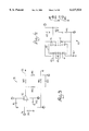
- FIG. 1 is a block diagram of a communication system constructed according to the invention.
- FIG. 2 is a schematic diagram of a transmitter of the communication system of FIG. 1.
- FIG. 3 is a schematic diagram of a baseband amplification circuit employed in the transmitter of FIG. 2.
- FIG. 4 is a schematic diagram of a current driver circuit employed in the transmitter of FIG. 2.
- FIG. 5 is a schematic diagram of a receiver of the communication system of FIG. 1.
- FIG. 6 is a schematic diagram of a line equalization circuit employed in the receiver of FIG. 5.
- FIG. 7 is a schematic diagram of a current/noise suppression circuit employed in the receiver of FIG. 5.
- FIG. 8 is a schematic diagram of a signal equalization circuit employed in the receiver of FIG. 5.
- FIG. 9 is a block diagram of a variation of the communication system of FIG. 1.
- FIG. 10 is a block diagram of a variation of the communication system of FIG. 9.
- FIG. 11a illustrates the non-inverted component of a video signal in differential mode.
- FIG. 11b illustrates the inverted component of a video signal in differential mode.
- FIG. 12 illustrates a current driven video signal in differential mode transmitted over a wire pair link.
- FIG. 13a illustrates a video signal at the input to the transmitter of FIG. 2.
- FIG. 13b illustrates a video signal at the input to the receiver of FIG. 5.
- FIG. 13c illustrates a video signal at the output of the line equalization circuit of FIG. 6.
- FIG. 13d illustrates a video signal at the output of the current/noise suppression circuit of FIG. 7.
- FIG. 13e illustrates a video signal at the output of the signal equalization circuit of FIG. 8.
- FIG. 1 illustrates a communication system 1 comprised of a transmitting terminal 5 and a receiving terminal 55 connected by a wire pair link 50.
- a video signal source 6, a telephone signal source 7, and a data signal source 8 are coupled to a multiplexer circuit 15.
- the multiplexer circuit 15 is coupled to a transmitter 20 having a baseband amplification circuit 30 and a current driver circuit 40.
- the transmitter 20 is coupled to the first end of the wire pair link 50.
- the second end of the wire pair link 50 is coupled to a receiver 60 having a line equalization circuit 70, a current/noise suppression circuit 80, and a signal equalization circuit 90.
- the receiver 60 is coupled to a demultiplexer circuit 105 and a lowpass filter/driver circuit 104.
- the demultiplexer circuit 105 is coupled to a video signal receiver 110, a telephone signal receiver 111, and a data signal receiver 112, and the lowpass filter/driver circuit 104 is coupled to the video signal receiver 110.
- the signal sources of the transmitting terminal 5 are illustrated in FIG. 1.
- the signal sources include a video signal source 6, such as a video camera, a telephone signal source 7, such as a telephone handset, and a data signal source 8, such as a modem. Although only one video signal source 6, one telephone signal source 7, and one data signal source 8 are depicted, the communication system 1 is capable of handling a plurality of video and voice band signal sources.
- the video signal source 6 produces a signal with an audio component 9 and a video component 10, which has a bandwidth of at least 4.2 megahertz, and preferably 6.0 megahertz.
- the telephone signal source 7 produces a telephone signal 11 with a bandwidth of 4 kilohertz.
- the data signal source 8 produces a data signal 12 with a bandwidth of 4 kilohertz.
- the multiplexer circuit 15 multiplexes the audio component 9 and the video component 10 of the video signal, the telephone signal 11, and the data signal 12 to form a composite signal 16. Any multiplexer made by a variety of manufacturers may be used.
- the composite signal output 16 of the multiplexer circuit 15 is coupled to the transmitter 20.
- the transmitter 20 is illustrated schematically in FIG. 2.
- the composite signal output 16 of the multiplexer circuit 15 is coupled to an input line 21 of the transmitter 20.
- the transmitter 20 is comprised of a transmitter chip 25, external capacitors 2C1 and 2C2, an external variable capacitor 2C3, and external inductors 2L1 and 2L2.
- the transmitter chip 25 is comprised of a baseband amplification circuit 30 illustrated schematically in FIG. 3 and a current driver circuit 40 illustrated schematically in FIG. 4.
- the transmitter chip 25 is powered by a +5 volt DC power supply and a -5 volt DC power supply.
- the +5 volt DC power supply is connected to the external capacitor 2C2 and the external inductor 2L2, and the -5 volt DC power supply is connected to the external capacitor 2C1 and the external inductor 2L1.
- the values of 2C1, 2L1, 2C2, and 2L2 are dependent on the DC power supply used and on the application. If a clean DC power supply is used, capacitors 2C1 and 2C2 and inductors 2L1 and 2L2 are not needed.
- the input line 21 of the transmitter 20 is connected to the baseband amplification circuit 30.
- the baseband amplification circuit 30 is illustrated schematically in FIG. 3.
- the input line 21 of the transmitter 20 is connected to an input line 31 of the baseband amplification circuit 30.
- the baseband amplification circuit 30 employs an operational amplifier 32, such as model AD811 by Analog Device, resistors 3R1, 3R2, 3R3, 3R4, and 3R5 having values of 75 ohms, 750 ohms, 750 ohms, 195 ohms, and 75 ohms respectively, and capacitors 3C1, 3C2, and 3C3 having values of 0.1 microfarads, 0.1 microfarads, and 100 picofarads respectively.
- an operational amplifier 32 such as model AD811 by Analog Device
- resistors 3R1, 3R2, 3R3, 3R4, and 3R5 having values of 75 ohms, 750 ohms, 750 ohms, 195 ohms, and 75 ohms respectively
- capacitors 3C1, 3C2, and 3C3 having values of 0.1 microfarads, 0.1 microfarads, and 100 picofarads respectively.
- the operational amplifier 32, resistor 3R3, and capacitor 3C3 are used to amplify substantially the entire frequency spectrum of the composite signal, including the low and high frequencies.
- the baseband amplification circuit 30 also employs an external variable capacitor 2C3 (FIG. 2).
- Capacitor 2C3 is used to refine the high frequencies of the composite signal.
- the value of 2C3 will vary from 4 picofarads to 24 picofarads, depending on the frequency bandwidth of the composite signal.
- the output line 35 of the baseband amplification circuit 30 is connected to the current driver circuit 40.
- the current driver circuit 40 is illustrated schematically in FIG. 4.
- the output line 35 of the baseband amplification circuit 30 is connected to an input line 41 of the current driver circuit 40.
- the current driver circuit 40 employs a model Max 435 non-feedback transconducting amplifier by Maxim 43, resistors 4R1, 4R2, 4R3, and 4R4 having values of 495 ohms, 4.7K ohms, 34.8 ohms, and 34.8 ohms respectively, and capacitors 4C1, 4C2, and 4C3 having values 0.22 microfarads, 0.22 microfarads, and 0.22 microfarads respectively. It should be noted that if a different model non-feedback transconducting amplifier is used, the circuit configuration will change.
- the non-feedback transconducting amplifier 43 is used to convert the composite signal from common mode to differential mode.
- the differential composite signal has a non-inverted component and an inverted component.
- FIGS. 11a and 11b illustrate a signal in differential mode.
- the non-inverted component of a differential video signal is illustrated in FIG. 11a, and the inverted component of a differential video signal is illustrated in FIG. 11b.
- the non-feedback transconducting amplifier 43 then adds a 90 degree current to the non-inverted component of the differential composite signal and a -90 degree current to the inverted component of the differential composite signal.
- Resistor 4R2 and capacitor 4C2 are used to set and reset the time constant of the current.
- the non-inverted component of the differential composite signal driven by the 90 degree current appears on line 46.
- the inverted component of the differential composite signal driven by the -90 degree current appears on line 47.
- Resistors 4R3 and 4R4 are used to match the resistance of the wire pair link 50. Because the resistance of a wire is constant, independent of the length of the wire, the values of 4R3 and 4R4 will not vary with the length of the wire pair link 50.
- Output lines 48 and 49 of the current driver circuit 40 are connected to output lines 27 and 28 of the transmitter 20.
- Output lines 27 and 28 of the transmitter 20 are coupled to the first end of the wire pair link 50.
- the wire pair link 50 is illustrated in FIG. 1. Output lines 27 and 28 of the transmitter 20 of the transmitting terminal 5 are coupled to the first end of the wire pair link 50.
- the wire pair link 50 is comprised of a first wire 51 and a second wire 52.
- the first wire 51 carries the non-inverted component of the differential composite signal driven by the 90 degree current.
- the second wire carries the inverted component of the differential composite signal driven by the -90 degree current.
- the 90 degree current on the first wire 51 and the -90 degree current on the second wire 52 cancel each other with a phase shift error of 10 -24 . Therefore, crosstalk is almost completely eliminated.
- the wire pair link 50 has a known impedance and capacitance which is dependent on the type and length of the wire used.
- the first wire 51 and the second wire 52 of the wire pair link 50 will typically be conventional telephone twisted pair; however, any copper wire may be used, including untwisted, shielded, or unshielded wire.
- the transmitter 20 is capable of driving the differential composite signal up to a distance of 5000 feet. The transmission distance can be extended to 15,000 feet by adding additional circuits to increase the current driving the signal.
- FIGS. 13a and 13b illustrate the effect that the wire pair link 50 has on the signal.
- FIG. 13a illustrates a video signal at the transmitter 20. As the video signal is transmitted over the wire pair link 50, it is degraded due to the impedance and capacitance of the line. The degraded video signal is illustrated in FIG. 13b. As shown, the video signal has lost linearity and amplitude.
- the second end of the wire pair link 50 is coupled to the receiver 60 of the receiving terminal 55.
- the receiver 60 is illustrated schematically in FIG. 5.
- the second end of the wire pair link 50 is coupled to input lines 61 and 62 of the receiver 60.
- the receiver 60 is comprised of a receiver chip 63, external variable resistors 5R1, 5R2, 5R3, and 5R5, external resistors 5R4, 5R6, and 5R7, an external variable capacitor 5C1, and a dip switch 64.
- the receiver chip 63 is comprised of a line equalization circuit illustrated schematically in FIG. 6, a current/noise suppression circuit illustrated schematically in FIG. 7, and a signal equalization circuit illustrated schematically in FIG. 8. As illustrated in FIG. 5, the receiver chip 63 is powered by a +5 volt DC power supply and a -5 volt DC power supply.
- the input lines 61 and 62 of the receiver 60 are connected to the line equalization circuit 70.
- the line equalization circuit 70 is illustrated schematically in FIG. 6.
- the input lines 61 and 62 of the receiver 60 are connected to input lines 71 and 72 of the line equalization circuit 70.
- the line equalization circuit employs a model Max 436 non-feedback transconducting amplifier by Maxim 73, resistors 6R1, 6R2, and 6R3 having values of 60 ohms, 100 ohms, and 4.7K ohms respectively, capacitors 6C1, 6C2, 6C3, 6C4, 6C5, and 6C6 having values of 1000 picofarads, 1000 picofarads, 1000 picofarads, 0.1 microfarads, 0.22 microfarads, and 0.22 microfarads respectively, external resistors 5R4, 5R6, and 5R7 (FIG.
- Resistors 5R6 and 5R7 almost completely eliminate the small amount of crosstalk from the wire pair link 50.
- Resistor 6R1 provides an offset impedance to the differential composite signal to correct for the degradation caused by the impedance of the wire pair link 50.
- Variable resistor 5R1 attenuates the differential composite signal to compensate for the gain from the transmitter 20.
- the value of 5R1 will vary from 1K ohms to 2K ohms, depending on the type and length of the wire used in the wire pair link 50.
- Resistor 6R2 and variable resistor 5R3 adjust the linearity of the differential composite signal
- resistor 5R4 and variable resistor 5R5 adjust the linearity of the high frequencies.
- the value of 5R3 will vary from 0 ohms to 1K ohms
- the value of 5R5 will vary from 0 ohms to 500 ohms, depending on the type and length of the wire used in the wire pair link 50.
- Capacitors 6C1, 6C2, and 6C3 and variable capacitor 5C1 provide an offset capacitance to the differential composite signal to correct for the degradation caused by the capacitance of the wire pair link 50.
- the value of 5C1 will vary from 10 picofarads to 180 picofarads, depending on the type and length of the wire used in the wire pair link 50.
- the positions of each of the three switches in the dip switch 64 will also vary depending on the type and length of the wire used in the wire pair link 50.
- the non-feedback transconducting amplifier 73 is used to convert the composite signal from differential mode to common mode and to strip the -90 degree current from the composite signal.
- FIGS. 13b and 13c illustrate the effect that the line equalization circuit 70 has on a signal.
- the degraded video signal appearing at the input to the receiver 60 is illustrated in FIG. 13b.
- the line equalization circuit 70 amplifies the signal and corrects some of the loss of linearity
- the partially reconstructed video signal appearing at the output of the line equalization circuit 70 is illustrated in FIG. 13c.
- the output line 75 of the line equalization circuit 70 is connected to the current/noise suppression circuit 80.
- the current/noise suppression circuit 80 is illustrated schematically in FIG. 7.
- the output line 75 of the line equalization circuit 70 is connected to an input line 81 of the current/noise suppression circuit 80.
- the current/noise suppression circuit 80 employs a transistor 83, such as model MMBT 4124 by National, and resistors 7R1, 7R2, 7R3, 7R4, 7R5, and 7R6 having values of 169 ohms, 75 ohms, 27K ohms, 39K ohms, 1K ohms, and 139 ohms respectively.
- a transistor 83 such as model MMBT 4124 by National
- resistors 7R1, 7R2, 7R3, 7R4, 7R5, and 7R6 having values of 169 ohms, 75 ohms, 27K ohms, 39K ohms, 1K ohms, and 139 ohms respectively.
- Resistors 7R1, 7R2, and 7R6 strip the 90 degree current from the composite signal. Resistors 7R1 and 7R2 suppress the noise in the composite signal. Resistors 7R3 and 7R4 bias the transistor 83, as well as suppress noise. Resistor 7R6 adjusts the gain of the composite signal.
- FIGS. 13c and 13d illustrate the effect that the current/noise suppression circuit 80 has on a signal.
- the partially reconstructed video signal appearing at the input to the current/noise suppression circuit 80 is illustrated in FIG. 13c.
- the current/noise suppression circuit 80 suppresses the noise in the video signal.
- the video signal appearing at the output of the current/noise suppression circuit 80 is illustrated in FIG. 13d.
- the output line 85 of the current/noise suppression circuit 80 is connected to the signal equalization circuit 90 through an external variable resistor 5R2.
- the signal equalization circuit 90 is illustrated schematically in FIG. 8.
- the output line 85 of the current/noise suppression circuit 80 is connected to input lines 91 and 92 of the signal equalization circuit 90 through an external variable resistor 5R2 (FIG. 5).
- Variable resistor 5R2 is used to adjust the gain of the composite signal.
- the value of 5R2 will vary from 0 ohms to 1K ohms, depending on the type and length of the wire used in the wire pair link 50.
- the signal equalization circuit 90 has three stages: stage one 93, stage two 94, and stage three 95, which use sin x/x correction to amplify and refine the composite signal.
- sin x/x correction means that the negative component and the positive component of the composite signal are alternately amplified and refined to balance the signal.
- stage one 93 the negative component of the composite signal is refined and amplified to approximately 98% of its original amplitude, which causes the positive component to lose approximately 20% of its amplitude.
- stage two 94 the positive component of the composite signal is refined and amplified to approximately 100% of its original amplitude, which causes the negative component to lose approximately 5-10% of its amplitude.
- stage three 95 the negative component is refined and amplified to approximately 100% of its original amplitude.
- both the positive and negative components of the composite signal have been equalized.
- FIGS. 13d and 13e illustrate the effect that sin x/x correction has on a signal.
- FIG. 13d illustrates a video signal appearing at the input to the signal equalization circuit 90.
- the positive and negative components of the video signal are amplified and refined.
- the reconstructed video signal appearing at the output of the signal equalization circuit 90 is illustrated in FIG. 13e. Therefore, at the output of the signal equalization circuit 90, the video signal is almost completely restored.
- Stage one 93 of the signal equalization circuit 90 employs an operational amplifier 96, such as model AD811 by Analog Device, resistors 8R1, 8R2, 8R3, 8R4, 8R5, and 8R6 having values of 100 ohms, 2.7K ohms, 10 ohms, 24K ohms, 750 ohms, and 750 ohms respectively, and capacitors 8C1 and 8C2 having values of 0.1 microfarads and 0.1 microfarads respectively.
- an operational amplifier 96 such as model AD811 by Analog Device
- resistors 8R1, 8R2, 8R3, 8R4, 8R5, and 8R6 having values of 100 ohms, 2.7K ohms, 10 ohms, 24K ohms, 750 ohms, and 750 ohms respectively
- capacitors 8C1 and 8C2 having values of 0.1 microfarads and 0.1 microfarad
- Stage two 94 of the signal equalization circuit 90 employs an operational amplifier 97, such as model AD811 by Analog Device, resistors 8R7, 8R8, 8R9, and 8R10 having values of 75 ohms, 750 ohms, 14.5K ohms, and 750 ohms respectively, and capacitors 8C3 and 8C4 having values of 0.1 microfarads and 0.1 microfarads respectively.
- an operational amplifier 97 such as model AD811 by Analog Device
- resistors 8R7, 8R8, 8R9, and 8R10 having values of 75 ohms, 750 ohms, 14.5K ohms, and 750 ohms respectively
- capacitors 8C3 and 8C4 having values of 0.1 microfarads and 0.1 microfarads respectively.
- Stage three 95 of the signal equalization circuit 90 employs an operational amplifier 98, such as model AD811 by Analog Device, resistors 8R11, 8R12, 8R13, 8R14, 8R15, 8R16, and 8R17 having values of 75 ohms, 175 ohms, 1.2K ohms, 2K ohms, 1.75K ohms, 75 ohms, and 75 ohms respectively, and capacitors 8C5 and 8C6 having values of 0.1 microfarads and 0.1 microfarads respectively.
- an operational amplifier 98 such as model AD811 by Analog Device
- resistors 8R11, 8R12, 8R13, 8R14, 8R15, 8R16, and 8R17 having values of 75 ohms, 175 ohms, 1.2K ohms, 2K ohms, 1.75K ohms, 75 ohms, and 75
- the composite signal appears at each of output lines 99 and 100 of the signal equalization circuit 90.
- This composite signal has less than 1% error compared to the composite signal output 16 of the multiplexer circuit 15 (FIG. 1). Therefore, although additional stages may be used to further amplify and refine the composite signal, they are not required.
- the composite signal on output line 99 is connected to output line 65 of the receiver 60, which is coupled to the lowpass filter/driver circuit 104.
- the composite signal on output line 100 is connected to output line 66 of the receiver 60, which is coupled to the demultiplexer circuit 105.
- the composite signal appearing on output line 65 of the receiver 60 is coupled to the lowpass filter/driver circuit 104.
- the lowpass filter/driver circuit 104 removes the video component 106 of the video signal from the composite signal, maintaining the signal to noise ratio of the video component 106. Any lowpass filter and driver made by a variety of manufacturers may be used.
- the video component 106 of the video signal is coupled to the video signal receiver 110.
- the composite signal appearing on output line 66 of the receiver 60 is coupled to the demultiplexer circuit 105.
- the demultiplexer circuit 105 demultiplexes the composite signal into the telephone signal 108, the data signal 109, and the audio component 107 of the video signal. Any demultiplexer made by a variety of manufacturers may be used. These signals are coupled to corresponding signal receivers.
- the signal receivers are illustrated in FIG. 1.
- the video component 106 and the audio component 107 of the video signal are coupled to a video signal receiver 110, such as a television set.
- the telephone signal 108 is coupled to a telephone signal receiver 111, such as a telephone handset.
- the data signal 109 is coupled to a data signal receiver 112, such as a data modem receiving module.
- the transmitter 20 is capable of transmitting a composite signal with a bandwidth of up to 350 megahertz over the wire pair link 50 to the receiver 60.
- the communication system's bandwidth capability is dependent on the length of the wire pair link 50. For example, a 350 megahertz composite signal can be transmitted up to 1000 feet, a 12 megahertz composite signal up to 3500 feet, and an 8 megahertz composite signal up to 5000 feet.
- the communication system of FIG. 1 includes a current/noise suppression circuit 80 which strips the current from the composite signal. Certain applications, however, will not require the current to be stripped from the signal, such as driving an LED.
- the communication system of FIG. 1 also includes a line equalization circuit 70 which converts the composite signal from differential mode to common mode. Certain applications, however, will require that the composite signal remain in differential mode.
- the communication system of FIG. 1 illustrates a transmitting terminal 5 on one end of the communication system 1 and a receiving terminal 55 on the other end of the communication system 1. It is to be understood, however, that in most applications each end of the communication system 1 will have both a transmitting terminal 5 and a receiving terminal 55 to allow for bi-directional communication.
- FIG. 9 is a block diagram of such a system.
- a first station 120 is comprised of a plurality of signal sources 125, a multiplexer circuit 121, and a transmitter 122, as well as a receiver 124, a demultiplexer circuit 123, a lowpass filter/driver circuit 127, and a plurality of signal receivers 126.
- a second station 130 is comprised of a receiver 131, a demultiplexer circuit 132, a lowpass filter/driver circuit 137, and a plurality of signal receivers 135, as well as a plurality of signal sources 136, a multiplexer circuit 134, and a transmitter 133.
- FIG. 9 illustrates two stations 120 and 130 which are connected directly to each other by two pair of wire 140 and 141, typically telephone twisted pair. It is to be understood, however, that the system is equally applicable to stations connected in a nationwide telecommunication network.
- FIG. 10 illustrates such a system.
- a first station 151 typically a home or business, is connected to a hub 152 by two pair of telephone wire 157.
- the hub 152 is centrally located so as to serve many homes or businesses.
- the hub 152 is connected to a telephone central office 153 by fiber optic cable 158.
- the central office 153 is connected to another telephone central office 154 by a nationwide telecommunication network which can include fiber optic cable, microwave, and satellites, indicated generally at 159.
- the central office 154 is connected to a hub 155 by fiber optic cable 160.
- the hub 155 is connected to a second station 156 by two pair of telephone wire 161.
- the preferred embodiments of the communication system of the invention provide for the transmission of non-compressed video, voice and data with little loss of signal between stations located on the same floor, in the same building, or in the same complex of buildings, as well as between stations located in different parts of the country.
- the clarity of the signal at the signal receivers is dependent on the length of the wire pair link 50.
- the signal to noise ratio is 62 dB and 48 dB at 3200 feet and 5000 feet respectively.
- the signal to noise ratio can easily be increased to 75 dB at 5000 feet by using a second non-feedback transconducting amplifier at the transmitter and a second pair of wire. Accordingly, the scope of the invention should not be construed as limited to the specific embodiment of the communication system depicted and described, but rather is defined in the claims appended hereto.
Abstract
Description
Claims (13)
Priority Applications (1)
| Application Number | Priority Date | Filing Date | Title |
|---|---|---|---|
| US08/550,359 US6137524A (en) | 1995-10-30 | 1995-10-30 | Transmitter and receiver circuits for transmission of voice, data and video signals for extended distances |
Applications Claiming Priority (1)
| Application Number | Priority Date | Filing Date | Title |
|---|---|---|---|
| US08/550,359 US6137524A (en) | 1995-10-30 | 1995-10-30 | Transmitter and receiver circuits for transmission of voice, data and video signals for extended distances |
Publications (1)
| Publication Number | Publication Date |
|---|---|
| US6137524A true US6137524A (en) | 2000-10-24 |
Family
ID=24196839
Family Applications (1)
| Application Number | Title | Priority Date | Filing Date |
|---|---|---|---|
| US08/550,359 Expired - Fee Related US6137524A (en) | 1995-10-30 | 1995-10-30 | Transmitter and receiver circuits for transmission of voice, data and video signals for extended distances |
Country Status (1)
| Country | Link |
|---|---|
| US (1) | US6137524A (en) |
Cited By (15)
| Publication number | Priority date | Publication date | Assignee | Title |
|---|---|---|---|---|
| US20030188069A1 (en) * | 2002-03-29 | 2003-10-02 | Serge Bedwani | In-protocol impedance compensation control |
| US20040059598A1 (en) * | 2002-09-24 | 2004-03-25 | David L. Wellons | Network-based healthcare information systems |
| US20040125937A1 (en) * | 2002-12-31 | 2004-07-01 | Turcan Diane Brown | Computer telephony integration (CTI) complete customer contact center |
| US20040125940A1 (en) * | 2002-12-31 | 2004-07-01 | Turcan Diane Brown | Computer telephony integration (CTI) complete hospitality contact center |
| US20040125938A1 (en) * | 2002-12-31 | 2004-07-01 | Turcan Diane Brown | Computer telephony integration (CTI) complete healthcare contact center |
| US20040148194A1 (en) * | 2003-01-27 | 2004-07-29 | Wellons David L. | Virtual physician office systems and methods |
| US20040146156A1 (en) * | 2003-01-27 | 2004-07-29 | Wellons David L. | Healthcare virtual private network methods and systems |
| US20040146047A1 (en) * | 2003-01-27 | 2004-07-29 | Turcan Diane Brown | Computer telephony integration (CTI) systems and methods for enhancing school safety |
| US20060126862A1 (en) * | 1997-08-15 | 2006-06-15 | Leisuretech Electronics Pty., Ltd. | Distributed audio system |
| US7149242B1 (en) * | 2000-05-31 | 2006-12-12 | Bitrage, Inc. | Communications system for improving transmission rates and transmission distances of data signals across communications links |
| US20080005042A1 (en) * | 2006-06-28 | 2008-01-03 | Pitney Bowes Incorporated | Postage printing system for printing both postal and non-postal documents |
| US7376704B2 (en) | 2002-09-24 | 2008-05-20 | At&T Delaware Intellectual Property, Inc. | Methods, systems, and products for converting between legacy systems |
| US20090074102A1 (en) * | 2007-09-17 | 2009-03-19 | Oxford J Craig | Method and apparatus for wired signal transmission |
| US20090262794A1 (en) * | 1997-06-20 | 2009-10-22 | Massachusetts Institute Of Technology | Digital transmitter |
| US20100083340A1 (en) * | 2008-09-26 | 2010-04-01 | Pelco, Inc | Line Tapping Method of Video Amplification for Unshielded Twisted Pair Active Receiver |
Citations (23)
| Publication number | Priority date | Publication date | Assignee | Title |
|---|---|---|---|---|
| US3872253A (en) * | 1972-05-24 | 1975-03-18 | John J Jurschak | Signal transmission and surveillance system using a subscriber{3 s telephone line without interfering with normal telephone line operation |
| US4030027A (en) * | 1974-11-06 | 1977-06-14 | Nippon Kokan Kabushiki Kaisha | Apparatus for non-contact measurement of distance from a metallic body using a detection coil in the feedback circuit of an amplifier |
| US4054910A (en) * | 1976-02-26 | 1977-10-18 | Tel-E-Tel, Inc. | Communication system for the transmission of closed circuit television over an ordinary pair of wires |
| US4525677A (en) * | 1983-10-12 | 1985-06-25 | The Grass Valley Group, Inc. | Differential amplifier having high common-mode rejection ratio |
| US4679209A (en) * | 1985-02-13 | 1987-07-07 | Northern Telecom Limited | Digital line receiver |
| US4714959A (en) * | 1986-07-22 | 1987-12-22 | Vicon Industries, Inc. | Bi-directional amplifier for control and video signals in a closed circuit television system |
| US4980887A (en) * | 1988-10-27 | 1990-12-25 | Seiscor Technologies | Digital communication apparatus and method |
| US4995031A (en) * | 1989-06-19 | 1991-02-19 | Northern Telecom Limited | Equalizer for ISDN-U interface |
| US5130793A (en) * | 1988-07-22 | 1992-07-14 | Etat Francais | Reconfigurable multiple-point wired in-house network for simultaneous and/or alternative distribution of several types of signals, notably baseband images, and method for the configuration of a system such as this |
| US5187446A (en) * | 1992-06-10 | 1993-02-16 | Digital Equipment Corporation | Feedback isolation amplifier |
| US5283637A (en) * | 1990-08-20 | 1994-02-01 | Christine Holland Trustee/Goolcharan Trust | Telecommunication system for transmitting full motion video |
| US5283789A (en) * | 1992-05-15 | 1994-02-01 | Private Satellite Network, Inc. | Communication system providing data and television signals to PC work stations |
| US5347305A (en) * | 1990-02-21 | 1994-09-13 | Alkanox Corporation | Video telephone system |
| US5367273A (en) * | 1992-09-11 | 1994-11-22 | At&T Corp. | Adapter for video and audio transmission |
| US5387927A (en) * | 1993-09-17 | 1995-02-07 | Mpr Teltech Ltd. | Method and apparatus for broadband transmission from a central office to a number of subscribers |
| US5408260A (en) * | 1994-01-11 | 1995-04-18 | Northern Telecom Limited | Customer premises ADSL signal distribution arrangement |
| WO1995011570A1 (en) * | 1993-10-20 | 1995-04-27 | Videolan Technologies, Inc. | A local area network for simultaneous, bi-directional transmission of video bandwidth signals |
| US5485488A (en) * | 1994-03-29 | 1996-01-16 | Apple Computer, Inc. | Circuit and method for twisted pair current source driver |
| US5523703A (en) * | 1993-09-17 | 1996-06-04 | Fujitsu Limited | Method and apparatus for controlling termination of current driven circuits |
| US5528286A (en) * | 1990-08-20 | 1996-06-18 | Christine Holland Trustee/Goolcharan Trust | Telecommunication system for transmitting full motion video |
| US5541957A (en) * | 1994-06-15 | 1996-07-30 | National Semiconductor Corporation | Apparatus for transmitting and/or receiving data at different data transfer rates especially in applications such as dual-rate ethernet local-area networks |
| US5592510A (en) * | 1994-03-29 | 1997-01-07 | Apple Computer, Inc. | Common mode early voltage compensation subcircuit for current driver |
| US5608464A (en) * | 1991-04-12 | 1997-03-04 | Scitex Corporation Ltd. | Digital video effects generator |
-
1995
- 1995-10-30 US US08/550,359 patent/US6137524A/en not_active Expired - Fee Related
Patent Citations (24)
| Publication number | Priority date | Publication date | Assignee | Title |
|---|---|---|---|---|
| US3872253A (en) * | 1972-05-24 | 1975-03-18 | John J Jurschak | Signal transmission and surveillance system using a subscriber{3 s telephone line without interfering with normal telephone line operation |
| US4030027A (en) * | 1974-11-06 | 1977-06-14 | Nippon Kokan Kabushiki Kaisha | Apparatus for non-contact measurement of distance from a metallic body using a detection coil in the feedback circuit of an amplifier |
| US4054910A (en) * | 1976-02-26 | 1977-10-18 | Tel-E-Tel, Inc. | Communication system for the transmission of closed circuit television over an ordinary pair of wires |
| US4525677A (en) * | 1983-10-12 | 1985-06-25 | The Grass Valley Group, Inc. | Differential amplifier having high common-mode rejection ratio |
| US4679209A (en) * | 1985-02-13 | 1987-07-07 | Northern Telecom Limited | Digital line receiver |
| US4714959A (en) * | 1986-07-22 | 1987-12-22 | Vicon Industries, Inc. | Bi-directional amplifier for control and video signals in a closed circuit television system |
| US5130793A (en) * | 1988-07-22 | 1992-07-14 | Etat Francais | Reconfigurable multiple-point wired in-house network for simultaneous and/or alternative distribution of several types of signals, notably baseband images, and method for the configuration of a system such as this |
| US4980887A (en) * | 1988-10-27 | 1990-12-25 | Seiscor Technologies | Digital communication apparatus and method |
| US4995031A (en) * | 1989-06-19 | 1991-02-19 | Northern Telecom Limited | Equalizer for ISDN-U interface |
| US5347305A (en) * | 1990-02-21 | 1994-09-13 | Alkanox Corporation | Video telephone system |
| US5528286A (en) * | 1990-08-20 | 1996-06-18 | Christine Holland Trustee/Goolcharan Trust | Telecommunication system for transmitting full motion video |
| US5283637A (en) * | 1990-08-20 | 1994-02-01 | Christine Holland Trustee/Goolcharan Trust | Telecommunication system for transmitting full motion video |
| US5608464A (en) * | 1991-04-12 | 1997-03-04 | Scitex Corporation Ltd. | Digital video effects generator |
| US5283789A (en) * | 1992-05-15 | 1994-02-01 | Private Satellite Network, Inc. | Communication system providing data and television signals to PC work stations |
| US5187446A (en) * | 1992-06-10 | 1993-02-16 | Digital Equipment Corporation | Feedback isolation amplifier |
| US5367273A (en) * | 1992-09-11 | 1994-11-22 | At&T Corp. | Adapter for video and audio transmission |
| US5523703A (en) * | 1993-09-17 | 1996-06-04 | Fujitsu Limited | Method and apparatus for controlling termination of current driven circuits |
| US5387927A (en) * | 1993-09-17 | 1995-02-07 | Mpr Teltech Ltd. | Method and apparatus for broadband transmission from a central office to a number of subscribers |
| WO1995011570A1 (en) * | 1993-10-20 | 1995-04-27 | Videolan Technologies, Inc. | A local area network for simultaneous, bi-directional transmission of video bandwidth signals |
| US5537142A (en) * | 1993-10-20 | 1996-07-16 | Videolan Technologies, Inc. | Local area network for simultaneous, bi-directional transmission of video bandwidth signals, including a switching matrix which defines user connections, upstream connections, and downstream connections and has an efficient configuration to minimize the |
| US5408260A (en) * | 1994-01-11 | 1995-04-18 | Northern Telecom Limited | Customer premises ADSL signal distribution arrangement |
| US5485488A (en) * | 1994-03-29 | 1996-01-16 | Apple Computer, Inc. | Circuit and method for twisted pair current source driver |
| US5592510A (en) * | 1994-03-29 | 1997-01-07 | Apple Computer, Inc. | Common mode early voltage compensation subcircuit for current driver |
| US5541957A (en) * | 1994-06-15 | 1996-07-30 | National Semiconductor Corporation | Apparatus for transmitting and/or receiving data at different data transfer rates especially in applications such as dual-rate ethernet local-area networks |
Cited By (54)
| Publication number | Priority date | Publication date | Assignee | Title |
|---|---|---|---|---|
| US8681837B2 (en) | 1997-06-20 | 2014-03-25 | Massachusetts Institute Of Technology | Digital Transmitter |
| US8989303B2 (en) | 1997-06-20 | 2015-03-24 | Massachusetts Institute Of Technology | Digital transmitter |
| US8238470B2 (en) | 1997-06-20 | 2012-08-07 | Massachusetts Institute Of Technology | Digital transmitter |
| US9419824B2 (en) | 1997-06-20 | 2016-08-16 | Massachusetts Institute Of Technology | Digital transmitter |
| US8238467B2 (en) * | 1997-06-20 | 2012-08-07 | Massachusetts Institute Of Technology | Digital transmitter |
| US8923433B2 (en) | 1997-06-20 | 2014-12-30 | Massachusetts Institute Of Technology | Digital transmitter |
| US8761235B2 (en) | 1997-06-20 | 2014-06-24 | Massachusetts Institute Of Technology | Digital transmitter |
| US20090262794A1 (en) * | 1997-06-20 | 2009-10-22 | Massachusetts Institute Of Technology | Digital transmitter |
| US9647857B2 (en) | 1997-06-20 | 2017-05-09 | Massachusetts Institute Of Technology | Digital transmitter |
| US20110200085A1 (en) * | 1997-06-20 | 2011-08-18 | Massachusetts Institute Of Technology | Digital Transmitter |
| US20110135032A1 (en) * | 1997-06-20 | 2011-06-09 | Massachusetts Institute Of Technology | Digital transmitter |
| US8311147B2 (en) | 1997-06-20 | 2012-11-13 | Massachusetts Institute Of Technology | Digital transmitter |
| US8259841B2 (en) | 1997-06-20 | 2012-09-04 | Massachusetts Institute Of Technology | Digital transmitter |
| US8254491B2 (en) | 1997-06-20 | 2012-08-28 | Massachusetts Institute Of Technology | Digital transmitter |
| US8243847B2 (en) | 1997-06-20 | 2012-08-14 | Massachusetts Institute Of Technology | Digital transmitter |
| US7756277B2 (en) * | 1997-08-15 | 2010-07-13 | Leisuretech Electronics Pty. Ltd. | Distributed audio system |
| US20060126862A1 (en) * | 1997-08-15 | 2006-06-15 | Leisuretech Electronics Pty., Ltd. | Distributed audio system |
| US7149242B1 (en) * | 2000-05-31 | 2006-12-12 | Bitrage, Inc. | Communications system for improving transmission rates and transmission distances of data signals across communications links |
| US7356555B2 (en) | 2002-03-29 | 2008-04-08 | Intel Corporation | In-protocol impedance compensation control |
| US20030188069A1 (en) * | 2002-03-29 | 2003-10-02 | Serge Bedwani | In-protocol impedance compensation control |
| WO2003085918A1 (en) * | 2002-03-29 | 2003-10-16 | Intel Corporation | In-protocol impedance compensation control |
| US8699688B2 (en) | 2002-09-24 | 2014-04-15 | At&T Intellectual Property I, L.P. | Network based healthcare information systems |
| US20040059598A1 (en) * | 2002-09-24 | 2004-03-25 | David L. Wellons | Network-based healthcare information systems |
| US7298836B2 (en) | 2002-09-24 | 2007-11-20 | At&T Bls Intellectual Property, Inc. | Network-based healthcare information systems |
| US7376704B2 (en) | 2002-09-24 | 2008-05-20 | At&T Delaware Intellectual Property, Inc. | Methods, systems, and products for converting between legacy systems |
| US9363376B2 (en) | 2002-12-31 | 2016-06-07 | At&T Intellectual Property I, L.P. | Methods, systems, and products for routing communications |
| US9794410B2 (en) | 2002-12-31 | 2017-10-17 | At&T Intellectual Property I, L.P. | Methods, systems, and products for routing communications |
| US20040125937A1 (en) * | 2002-12-31 | 2004-07-01 | Turcan Diane Brown | Computer telephony integration (CTI) complete customer contact center |
| US7620170B2 (en) * | 2002-12-31 | 2009-11-17 | At&T Intellectual Property I, L.P. | Computer telephony integration (CTI) complete customer contact center |
| US7573999B2 (en) * | 2002-12-31 | 2009-08-11 | At&T Intellectual Property I, L.P. | Computer telephony integration (CTI) complete healthcare contact center |
| US9258422B2 (en) | 2002-12-31 | 2016-02-09 | At&T Intellectual Property I, L.P. | Computer telephony integration complete healthcare contact center |
| US7356139B2 (en) | 2002-12-31 | 2008-04-08 | At&T Delaware Intellectual Property, Inc. | Computer telephony integration (CTI) complete hospitality contact center |
| US20040125940A1 (en) * | 2002-12-31 | 2004-07-01 | Turcan Diane Brown | Computer telephony integration (CTI) complete hospitality contact center |
| US9794408B2 (en) | 2002-12-31 | 2017-10-17 | At&T Intellectual Property I, L.P. | Routing of communications |
| US20040125938A1 (en) * | 2002-12-31 | 2004-07-01 | Turcan Diane Brown | Computer telephony integration (CTI) complete healthcare contact center |
| US8553870B2 (en) | 2002-12-31 | 2013-10-08 | At&T Intellectual Property I, L.P. | Computer telephony integration (CTI) complete healthcare contact center |
| US8767943B2 (en) | 2002-12-31 | 2014-07-01 | At&T Intellectual Property I, L.P. | Methods, systems, and products for routing communications to contact centers |
| US20040146156A1 (en) * | 2003-01-27 | 2004-07-29 | Wellons David L. | Healthcare virtual private network methods and systems |
| US9330133B2 (en) | 2003-01-27 | 2016-05-03 | At&T Intellectual Property I, L.P. | Virtual physician office systems and methods |
| US8712031B2 (en) | 2003-01-27 | 2014-04-29 | At&T Intellectual Property I, L.P. | Visual physician office systems and methods |
| US20040148194A1 (en) * | 2003-01-27 | 2004-07-29 | Wellons David L. | Virtual physician office systems and methods |
| US8638924B2 (en) | 2003-01-27 | 2014-01-28 | At&T Intellectual Property I, L.P. | Methods, systems, and products for exchanging health care communications |
| US7248688B2 (en) | 2003-01-27 | 2007-07-24 | Bellsouth Intellectual Property Corporation | Virtual physician office systems and methods |
| US10366786B2 (en) | 2003-01-27 | 2019-07-30 | At&T Intellectual Property I, L.P. | Methods, systems, and products for format conversion |
| US9659147B2 (en) | 2003-01-27 | 2017-05-23 | At&T Intellectual Property I, L.P. | Virtual physician office systems and methods |
| US20080091452A1 (en) * | 2003-01-27 | 2008-04-17 | Wellons David L | Visual physician office systems and methods |
| US20040146047A1 (en) * | 2003-01-27 | 2004-07-29 | Turcan Diane Brown | Computer telephony integration (CTI) systems and methods for enhancing school safety |
| US8149823B2 (en) | 2003-01-27 | 2012-04-03 | At&T Intellectual Property I, L.P. | Computer telephony integration (CTI) systems and methods for enhancing school safety |
| US7440567B2 (en) | 2003-01-27 | 2008-10-21 | At&T Intellectual Property I, L.P. | Healthcare virtual private network methods and systems |
| US20080005042A1 (en) * | 2006-06-28 | 2008-01-03 | Pitney Bowes Incorporated | Postage printing system for printing both postal and non-postal documents |
| US20090074102A1 (en) * | 2007-09-17 | 2009-03-19 | Oxford J Craig | Method and apparatus for wired signal transmission |
| US8948273B2 (en) * | 2007-09-17 | 2015-02-03 | J. Craig Oxford | Method and apparatus for wired signal transmission |
| US8059208B2 (en) | 2008-09-26 | 2011-11-15 | Pelco, Inc. | Line tapping method of video amplification for unshielded twisted pair active receiver |
| US20100083340A1 (en) * | 2008-09-26 | 2010-04-01 | Pelco, Inc | Line Tapping Method of Video Amplification for Unshielded Twisted Pair Active Receiver |
Similar Documents
| Publication | Publication Date | Title |
|---|---|---|
| US6137524A (en) | Transmitter and receiver circuits for transmission of voice, data and video signals for extended distances | |
| US7835516B2 (en) | Direct access arrangement device | |
| CA2114653C (en) | Method and apparatus for broadband transmission from a central office to a number of subscribers | |
| KR100338464B1 (en) | Method and system for transmitting video / data signal from device to communication network connection card | |
| US4054910A (en) | Communication system for the transmission of closed circuit television over an ordinary pair of wires | |
| US20020109771A1 (en) | Method and system for videoconferencing | |
| US6064422A (en) | Telecommunication system for broadcast quality video transmission | |
| US20060242682A1 (en) | An Optical Communication System for Transmitting RF Signals Downstream and Bidirectional Telephony Signals Which Also Include RF Control Signals Upstream | |
| US6393110B1 (en) | Methods and apparatus for terminating a line and supporting the asymmetric digital subscriber line protocol | |
| US20070022444A1 (en) | Software definable transceiver apparatus and method | |
| US20060080722A1 (en) | Buffered waveforms for high speed digital to analog conversion | |
| US20040233860A1 (en) | Signal distribution within customer premises | |
| US6574236B1 (en) | Interface device having VDSL splitter and interference filter | |
| KR101703808B1 (en) | Saystem and method for processing of cctv image using multiplexing scheme | |
| US20070022443A1 (en) | Interactive communication apparatus and system | |
| WO1998019457A1 (en) | Transmitter and receiver circuits for transmission of voice, data and video signals for extended distances | |
| DE60034281T2 (en) | An optical transmission system for optically combining baseband and transmission band signals | |
| JP3944139B2 (en) | TV door phone device | |
| US7953117B2 (en) | Home networking system | |
| JP4760586B2 (en) | Video transmission system | |
| US20070288988A1 (en) | Cable television system with extended quadrature amplitude modulation signal transmission, transmission means and a management centre therefor | |
| CA2384190C (en) | Apparatus and methods for extracting two distinct frequency bands from light received by a photodiode | |
| KR100992197B1 (en) | Home telephone line network system using ip based modem equipments | |
| NZ522126A (en) | Two way cable system with noise-free return path | |
| MXPA98008566A (en) | A method and system for transmiting video / data signals from a device towards a network of connection of the communication network |
Legal Events
| Date | Code | Title | Description |
|---|---|---|---|
| AS | Assignment |
Owner name: ISTHMUS TECHNOLOGY GROUP, L.P., KANSAS Free format text: ASSIGNMENT OF ASSIGNORS INTEREST;ASSIGNOR:CHEA, WOODY ALBERT;REEL/FRAME:007769/0211 Effective date: 19951029 |
|
| AS | Assignment |
Owner name: ISTHUMUS TECHNOLOGY GROUP, L.P., COLORADO Free format text: SECURITY INTEREST;ASSIGNOR:ZEKKO CORPORATION;REEL/FRAME:008854/0299 Effective date: 19971111 |
|
| AS | Assignment |
Owner name: ZEKKO CORPORATION, COLORADO Free format text: ASSIGNMENT OF ASSIGNORS INTEREST;ASSIGNOR:ISTHMUS TECHNOLOGY GROUP, L.P.;REEL/FRAME:008854/0356 Effective date: 19971202 |
|
| REMI | Maintenance fee reminder mailed | ||
| LAPS | Lapse for failure to pay maintenance fees | ||
| STCH | Information on status: patent discontinuation |
Free format text: PATENT EXPIRED DUE TO NONPAYMENT OF MAINTENANCE FEES UNDER 37 CFR 1.362 |
|
| FP | Lapsed due to failure to pay maintenance fee |
Effective date: 20041024 |