US6144093A - Commonly housed diverse semiconductor die with reduced inductance - Google Patents
Commonly housed diverse semiconductor die with reduced inductance Download PDFInfo
- Publication number
- US6144093A US6144093A US09/070,097 US7009798A US6144093A US 6144093 A US6144093 A US 6144093A US 7009798 A US7009798 A US 7009798A US 6144093 A US6144093 A US 6144093A
- Authority
- US
- United States
- Prior art keywords
- electrode
- die
- main pad
- pins
- source
- Prior art date
- Legal status (The legal status is an assumption and is not a legal conclusion. Google has not performed a legal analysis and makes no representation as to the accuracy of the status listed.)
- Expired - Lifetime
Links
Images


Classifications
-
- H—ELECTRICITY
- H01—ELECTRIC ELEMENTS
- H01L—SEMICONDUCTOR DEVICES NOT COVERED BY CLASS H10
- H01L24/00—Arrangements for connecting or disconnecting semiconductor or solid-state bodies; Methods or apparatus related thereto
- H01L24/01—Means for bonding being attached to, or being formed on, the surface to be connected, e.g. chip-to-package, die-attach, "first-level" interconnects; Manufacturing methods related thereto
- H01L24/02—Bonding areas ; Manufacturing methods related thereto
- H01L24/04—Structure, shape, material or disposition of the bonding areas prior to the connecting process
- H01L24/06—Structure, shape, material or disposition of the bonding areas prior to the connecting process of a plurality of bonding areas
-
- H—ELECTRICITY
- H01—ELECTRIC ELEMENTS
- H01L—SEMICONDUCTOR DEVICES NOT COVERED BY CLASS H10
- H01L23/00—Details of semiconductor or other solid state devices
- H01L23/48—Arrangements for conducting electric current to or from the solid state body in operation, e.g. leads, terminal arrangements ; Selection of materials therefor
- H01L23/488—Arrangements for conducting electric current to or from the solid state body in operation, e.g. leads, terminal arrangements ; Selection of materials therefor consisting of soldered or bonded constructions
- H01L23/495—Lead-frames or other flat leads
- H01L23/49541—Geometry of the lead-frame
- H01L23/49562—Geometry of the lead-frame for devices being provided for in H01L29/00
-
- H—ELECTRICITY
- H01—ELECTRIC ELEMENTS
- H01L—SEMICONDUCTOR DEVICES NOT COVERED BY CLASS H10
- H01L24/00—Arrangements for connecting or disconnecting semiconductor or solid-state bodies; Methods or apparatus related thereto
- H01L24/01—Means for bonding being attached to, or being formed on, the surface to be connected, e.g. chip-to-package, die-attach, "first-level" interconnects; Manufacturing methods related thereto
- H01L24/42—Wire connectors; Manufacturing methods related thereto
- H01L24/47—Structure, shape, material or disposition of the wire connectors after the connecting process
- H01L24/49—Structure, shape, material or disposition of the wire connectors after the connecting process of a plurality of wire connectors
-
- H—ELECTRICITY
- H01—ELECTRIC ELEMENTS
- H01L—SEMICONDUCTOR DEVICES NOT COVERED BY CLASS H10
- H01L24/00—Arrangements for connecting or disconnecting semiconductor or solid-state bodies; Methods or apparatus related thereto
- H01L24/80—Methods for connecting semiconductor or other solid state bodies using means for bonding being attached to, or being formed on, the surface to be connected
- H01L24/85—Methods for connecting semiconductor or other solid state bodies using means for bonding being attached to, or being formed on, the surface to be connected using a wire connector
-
- H—ELECTRICITY
- H01—ELECTRIC ELEMENTS
- H01L—SEMICONDUCTOR DEVICES NOT COVERED BY CLASS H10
- H01L2224/00—Indexing scheme for arrangements for connecting or disconnecting semiconductor or solid-state bodies and methods related thereto as covered by H01L24/00
- H01L2224/01—Means for bonding being attached to, or being formed on, the surface to be connected, e.g. chip-to-package, die-attach, "first-level" interconnects; Manufacturing methods related thereto
- H01L2224/02—Bonding areas; Manufacturing methods related thereto
- H01L2224/04—Structure, shape, material or disposition of the bonding areas prior to the connecting process
- H01L2224/04042—Bonding areas specifically adapted for wire connectors, e.g. wirebond pads
-
- H—ELECTRICITY
- H01—ELECTRIC ELEMENTS
- H01L—SEMICONDUCTOR DEVICES NOT COVERED BY CLASS H10
- H01L2224/00—Indexing scheme for arrangements for connecting or disconnecting semiconductor or solid-state bodies and methods related thereto as covered by H01L24/00
- H01L2224/01—Means for bonding being attached to, or being formed on, the surface to be connected, e.g. chip-to-package, die-attach, "first-level" interconnects; Manufacturing methods related thereto
- H01L2224/02—Bonding areas; Manufacturing methods related thereto
- H01L2224/04—Structure, shape, material or disposition of the bonding areas prior to the connecting process
- H01L2224/05—Structure, shape, material or disposition of the bonding areas prior to the connecting process of an individual bonding area
- H01L2224/0554—External layer
- H01L2224/0555—Shape
- H01L2224/05552—Shape in top view
-
- H—ELECTRICITY
- H01—ELECTRIC ELEMENTS
- H01L—SEMICONDUCTOR DEVICES NOT COVERED BY CLASS H10
- H01L2224/00—Indexing scheme for arrangements for connecting or disconnecting semiconductor or solid-state bodies and methods related thereto as covered by H01L24/00
- H01L2224/01—Means for bonding being attached to, or being formed on, the surface to be connected, e.g. chip-to-package, die-attach, "first-level" interconnects; Manufacturing methods related thereto
- H01L2224/02—Bonding areas; Manufacturing methods related thereto
- H01L2224/04—Structure, shape, material or disposition of the bonding areas prior to the connecting process
- H01L2224/05—Structure, shape, material or disposition of the bonding areas prior to the connecting process of an individual bonding area
- H01L2224/0554—External layer
- H01L2224/05599—Material
-
- H—ELECTRICITY
- H01—ELECTRIC ELEMENTS
- H01L—SEMICONDUCTOR DEVICES NOT COVERED BY CLASS H10
- H01L2224/00—Indexing scheme for arrangements for connecting or disconnecting semiconductor or solid-state bodies and methods related thereto as covered by H01L24/00
- H01L2224/01—Means for bonding being attached to, or being formed on, the surface to be connected, e.g. chip-to-package, die-attach, "first-level" interconnects; Manufacturing methods related thereto
- H01L2224/02—Bonding areas; Manufacturing methods related thereto
- H01L2224/04—Structure, shape, material or disposition of the bonding areas prior to the connecting process
- H01L2224/06—Structure, shape, material or disposition of the bonding areas prior to the connecting process of a plurality of bonding areas
- H01L2224/0601—Structure
- H01L2224/0603—Bonding areas having different sizes, e.g. different heights or widths
-
- H—ELECTRICITY
- H01—ELECTRIC ELEMENTS
- H01L—SEMICONDUCTOR DEVICES NOT COVERED BY CLASS H10
- H01L2224/00—Indexing scheme for arrangements for connecting or disconnecting semiconductor or solid-state bodies and methods related thereto as covered by H01L24/00
- H01L2224/01—Means for bonding being attached to, or being formed on, the surface to be connected, e.g. chip-to-package, die-attach, "first-level" interconnects; Manufacturing methods related thereto
- H01L2224/26—Layer connectors, e.g. plate connectors, solder or adhesive layers; Manufacturing methods related thereto
- H01L2224/31—Structure, shape, material or disposition of the layer connectors after the connecting process
- H01L2224/32—Structure, shape, material or disposition of the layer connectors after the connecting process of an individual layer connector
- H01L2224/321—Disposition
- H01L2224/32151—Disposition the layer connector connecting between a semiconductor or solid-state body and an item not being a semiconductor or solid-state body, e.g. chip-to-substrate, chip-to-passive
- H01L2224/32221—Disposition the layer connector connecting between a semiconductor or solid-state body and an item not being a semiconductor or solid-state body, e.g. chip-to-substrate, chip-to-passive the body and the item being stacked
- H01L2224/32245—Disposition the layer connector connecting between a semiconductor or solid-state body and an item not being a semiconductor or solid-state body, e.g. chip-to-substrate, chip-to-passive the body and the item being stacked the item being metallic
-
- H—ELECTRICITY
- H01—ELECTRIC ELEMENTS
- H01L—SEMICONDUCTOR DEVICES NOT COVERED BY CLASS H10
- H01L2224/00—Indexing scheme for arrangements for connecting or disconnecting semiconductor or solid-state bodies and methods related thereto as covered by H01L24/00
- H01L2224/01—Means for bonding being attached to, or being formed on, the surface to be connected, e.g. chip-to-package, die-attach, "first-level" interconnects; Manufacturing methods related thereto
- H01L2224/42—Wire connectors; Manufacturing methods related thereto
- H01L2224/44—Structure, shape, material or disposition of the wire connectors prior to the connecting process
- H01L2224/45—Structure, shape, material or disposition of the wire connectors prior to the connecting process of an individual wire connector
- H01L2224/45001—Core members of the connector
- H01L2224/45099—Material
- H01L2224/451—Material with a principal constituent of the material being a metal or a metalloid, e.g. boron (B), silicon (Si), germanium (Ge), arsenic (As), antimony (Sb), tellurium (Te) and polonium (Po), and alloys thereof
- H01L2224/45117—Material with a principal constituent of the material being a metal or a metalloid, e.g. boron (B), silicon (Si), germanium (Ge), arsenic (As), antimony (Sb), tellurium (Te) and polonium (Po), and alloys thereof the principal constituent melting at a temperature of greater than or equal to 400°C and less than 950°C
- H01L2224/45124—Aluminium (Al) as principal constituent
-
- H—ELECTRICITY
- H01—ELECTRIC ELEMENTS
- H01L—SEMICONDUCTOR DEVICES NOT COVERED BY CLASS H10
- H01L2224/00—Indexing scheme for arrangements for connecting or disconnecting semiconductor or solid-state bodies and methods related thereto as covered by H01L24/00
- H01L2224/01—Means for bonding being attached to, or being formed on, the surface to be connected, e.g. chip-to-package, die-attach, "first-level" interconnects; Manufacturing methods related thereto
- H01L2224/42—Wire connectors; Manufacturing methods related thereto
- H01L2224/47—Structure, shape, material or disposition of the wire connectors after the connecting process
- H01L2224/48—Structure, shape, material or disposition of the wire connectors after the connecting process of an individual wire connector
- H01L2224/4805—Shape
- H01L2224/4809—Loop shape
- H01L2224/48091—Arched
-
- H—ELECTRICITY
- H01—ELECTRIC ELEMENTS
- H01L—SEMICONDUCTOR DEVICES NOT COVERED BY CLASS H10
- H01L2224/00—Indexing scheme for arrangements for connecting or disconnecting semiconductor or solid-state bodies and methods related thereto as covered by H01L24/00
- H01L2224/01—Means for bonding being attached to, or being formed on, the surface to be connected, e.g. chip-to-package, die-attach, "first-level" interconnects; Manufacturing methods related thereto
- H01L2224/42—Wire connectors; Manufacturing methods related thereto
- H01L2224/47—Structure, shape, material or disposition of the wire connectors after the connecting process
- H01L2224/48—Structure, shape, material or disposition of the wire connectors after the connecting process of an individual wire connector
- H01L2224/4805—Shape
- H01L2224/4809—Loop shape
- H01L2224/48095—Kinked
- H01L2224/48096—Kinked the kinked part being in proximity to the bonding area on the semiconductor or solid-state body
-
- H—ELECTRICITY
- H01—ELECTRIC ELEMENTS
- H01L—SEMICONDUCTOR DEVICES NOT COVERED BY CLASS H10
- H01L2224/00—Indexing scheme for arrangements for connecting or disconnecting semiconductor or solid-state bodies and methods related thereto as covered by H01L24/00
- H01L2224/01—Means for bonding being attached to, or being formed on, the surface to be connected, e.g. chip-to-package, die-attach, "first-level" interconnects; Manufacturing methods related thereto
- H01L2224/42—Wire connectors; Manufacturing methods related thereto
- H01L2224/47—Structure, shape, material or disposition of the wire connectors after the connecting process
- H01L2224/48—Structure, shape, material or disposition of the wire connectors after the connecting process of an individual wire connector
- H01L2224/481—Disposition
- H01L2224/48135—Connecting between different semiconductor or solid-state bodies, i.e. chip-to-chip
- H01L2224/48137—Connecting between different semiconductor or solid-state bodies, i.e. chip-to-chip the bodies being arranged next to each other, e.g. on a common substrate
- H01L2224/48139—Connecting between different semiconductor or solid-state bodies, i.e. chip-to-chip the bodies being arranged next to each other, e.g. on a common substrate with an intermediate bond, e.g. continuous wire daisy chain
-
- H—ELECTRICITY
- H01—ELECTRIC ELEMENTS
- H01L—SEMICONDUCTOR DEVICES NOT COVERED BY CLASS H10
- H01L2224/00—Indexing scheme for arrangements for connecting or disconnecting semiconductor or solid-state bodies and methods related thereto as covered by H01L24/00
- H01L2224/01—Means for bonding being attached to, or being formed on, the surface to be connected, e.g. chip-to-package, die-attach, "first-level" interconnects; Manufacturing methods related thereto
- H01L2224/42—Wire connectors; Manufacturing methods related thereto
- H01L2224/47—Structure, shape, material or disposition of the wire connectors after the connecting process
- H01L2224/48—Structure, shape, material or disposition of the wire connectors after the connecting process of an individual wire connector
- H01L2224/481—Disposition
- H01L2224/48151—Connecting between a semiconductor or solid-state body and an item not being a semiconductor or solid-state body, e.g. chip-to-substrate, chip-to-passive
- H01L2224/48221—Connecting between a semiconductor or solid-state body and an item not being a semiconductor or solid-state body, e.g. chip-to-substrate, chip-to-passive the body and the item being stacked
- H01L2224/48245—Connecting between a semiconductor or solid-state body and an item not being a semiconductor or solid-state body, e.g. chip-to-substrate, chip-to-passive the body and the item being stacked the item being metallic
- H01L2224/48247—Connecting between a semiconductor or solid-state body and an item not being a semiconductor or solid-state body, e.g. chip-to-substrate, chip-to-passive the body and the item being stacked the item being metallic connecting the wire to a bond pad of the item
-
- H—ELECTRICITY
- H01—ELECTRIC ELEMENTS
- H01L—SEMICONDUCTOR DEVICES NOT COVERED BY CLASS H10
- H01L2224/00—Indexing scheme for arrangements for connecting or disconnecting semiconductor or solid-state bodies and methods related thereto as covered by H01L24/00
- H01L2224/01—Means for bonding being attached to, or being formed on, the surface to be connected, e.g. chip-to-package, die-attach, "first-level" interconnects; Manufacturing methods related thereto
- H01L2224/42—Wire connectors; Manufacturing methods related thereto
- H01L2224/47—Structure, shape, material or disposition of the wire connectors after the connecting process
- H01L2224/48—Structure, shape, material or disposition of the wire connectors after the connecting process of an individual wire connector
- H01L2224/484—Connecting portions
- H01L2224/4847—Connecting portions the connecting portion on the bonding area of the semiconductor or solid-state body being a wedge bond
- H01L2224/48472—Connecting portions the connecting portion on the bonding area of the semiconductor or solid-state body being a wedge bond the other connecting portion not on the bonding area also being a wedge bond, i.e. wedge-to-wedge
-
- H—ELECTRICITY
- H01—ELECTRIC ELEMENTS
- H01L—SEMICONDUCTOR DEVICES NOT COVERED BY CLASS H10
- H01L2224/00—Indexing scheme for arrangements for connecting or disconnecting semiconductor or solid-state bodies and methods related thereto as covered by H01L24/00
- H01L2224/01—Means for bonding being attached to, or being formed on, the surface to be connected, e.g. chip-to-package, die-attach, "first-level" interconnects; Manufacturing methods related thereto
- H01L2224/42—Wire connectors; Manufacturing methods related thereto
- H01L2224/47—Structure, shape, material or disposition of the wire connectors after the connecting process
- H01L2224/48—Structure, shape, material or disposition of the wire connectors after the connecting process of an individual wire connector
- H01L2224/485—Material
- H01L2224/48505—Material at the bonding interface
- H01L2224/48699—Principal constituent of the connecting portion of the wire connector being Aluminium (Al)
- H01L2224/487—Principal constituent of the connecting portion of the wire connector being Aluminium (Al) with a principal constituent of the bonding area being a metal or a metalloid, e.g. boron (B), silicon (Si), germanium (Ge), arsenic (As), antimony (Sb), tellurium (Te) and polonium (Po), and alloys thereof
- H01L2224/48738—Principal constituent of the connecting portion of the wire connector being Aluminium (Al) with a principal constituent of the bonding area being a metal or a metalloid, e.g. boron (B), silicon (Si), germanium (Ge), arsenic (As), antimony (Sb), tellurium (Te) and polonium (Po), and alloys thereof the principal constituent melting at a temperature of greater than or equal to 950°C and less than 1550°C
- H01L2224/48755—Nickel (Ni) as principal constituent
-
- H—ELECTRICITY
- H01—ELECTRIC ELEMENTS
- H01L—SEMICONDUCTOR DEVICES NOT COVERED BY CLASS H10
- H01L2224/00—Indexing scheme for arrangements for connecting or disconnecting semiconductor or solid-state bodies and methods related thereto as covered by H01L24/00
- H01L2224/01—Means for bonding being attached to, or being formed on, the surface to be connected, e.g. chip-to-package, die-attach, "first-level" interconnects; Manufacturing methods related thereto
- H01L2224/42—Wire connectors; Manufacturing methods related thereto
- H01L2224/47—Structure, shape, material or disposition of the wire connectors after the connecting process
- H01L2224/49—Structure, shape, material or disposition of the wire connectors after the connecting process of a plurality of wire connectors
- H01L2224/4901—Structure
- H01L2224/4903—Connectors having different sizes, e.g. different diameters
-
- H—ELECTRICITY
- H01—ELECTRIC ELEMENTS
- H01L—SEMICONDUCTOR DEVICES NOT COVERED BY CLASS H10
- H01L2224/00—Indexing scheme for arrangements for connecting or disconnecting semiconductor or solid-state bodies and methods related thereto as covered by H01L24/00
- H01L2224/01—Means for bonding being attached to, or being formed on, the surface to be connected, e.g. chip-to-package, die-attach, "first-level" interconnects; Manufacturing methods related thereto
- H01L2224/42—Wire connectors; Manufacturing methods related thereto
- H01L2224/47—Structure, shape, material or disposition of the wire connectors after the connecting process
- H01L2224/49—Structure, shape, material or disposition of the wire connectors after the connecting process of a plurality of wire connectors
- H01L2224/4905—Shape
- H01L2224/49051—Connectors having different shapes
-
- H—ELECTRICITY
- H01—ELECTRIC ELEMENTS
- H01L—SEMICONDUCTOR DEVICES NOT COVERED BY CLASS H10
- H01L2224/00—Indexing scheme for arrangements for connecting or disconnecting semiconductor or solid-state bodies and methods related thereto as covered by H01L24/00
- H01L2224/01—Means for bonding being attached to, or being formed on, the surface to be connected, e.g. chip-to-package, die-attach, "first-level" interconnects; Manufacturing methods related thereto
- H01L2224/42—Wire connectors; Manufacturing methods related thereto
- H01L2224/47—Structure, shape, material or disposition of the wire connectors after the connecting process
- H01L2224/49—Structure, shape, material or disposition of the wire connectors after the connecting process of a plurality of wire connectors
- H01L2224/491—Disposition
- H01L2224/4911—Disposition the connectors being bonded to at least one common bonding area, e.g. daisy chain
- H01L2224/49113—Disposition the connectors being bonded to at least one common bonding area, e.g. daisy chain the connectors connecting different bonding areas on the semiconductor or solid-state body to a common bonding area outside the body, e.g. converging wires
-
- H—ELECTRICITY
- H01—ELECTRIC ELEMENTS
- H01L—SEMICONDUCTOR DEVICES NOT COVERED BY CLASS H10
- H01L2224/00—Indexing scheme for arrangements for connecting or disconnecting semiconductor or solid-state bodies and methods related thereto as covered by H01L24/00
- H01L2224/73—Means for bonding being of different types provided for in two or more of groups H01L2224/10, H01L2224/18, H01L2224/26, H01L2224/34, H01L2224/42, H01L2224/50, H01L2224/63, H01L2224/71
- H01L2224/732—Location after the connecting process
- H01L2224/73251—Location after the connecting process on different surfaces
- H01L2224/73265—Layer and wire connectors
-
- H—ELECTRICITY
- H01—ELECTRIC ELEMENTS
- H01L—SEMICONDUCTOR DEVICES NOT COVERED BY CLASS H10
- H01L2224/00—Indexing scheme for arrangements for connecting or disconnecting semiconductor or solid-state bodies and methods related thereto as covered by H01L24/00
- H01L2224/80—Methods for connecting semiconductor or other solid state bodies using means for bonding being attached to, or being formed on, the surface to be connected
- H01L2224/85—Methods for connecting semiconductor or other solid state bodies using means for bonding being attached to, or being formed on, the surface to be connected using a wire connector
- H01L2224/852—Applying energy for connecting
- H01L2224/85201—Compression bonding
- H01L2224/85205—Ultrasonic bonding
-
- H—ELECTRICITY
- H01—ELECTRIC ELEMENTS
- H01L—SEMICONDUCTOR DEVICES NOT COVERED BY CLASS H10
- H01L2224/00—Indexing scheme for arrangements for connecting or disconnecting semiconductor or solid-state bodies and methods related thereto as covered by H01L24/00
- H01L2224/80—Methods for connecting semiconductor or other solid state bodies using means for bonding being attached to, or being formed on, the surface to be connected
- H01L2224/85—Methods for connecting semiconductor or other solid state bodies using means for bonding being attached to, or being formed on, the surface to be connected using a wire connector
- H01L2224/8538—Bonding interfaces outside the semiconductor or solid-state body
- H01L2224/85399—Material
- H01L2224/854—Material with a principal constituent of the material being a metal or a metalloid, e.g. boron (B), silicon (Si), germanium (Ge), arsenic (As), antimony (Sb), tellurium (Te) and polonium (Po), and alloys thereof
- H01L2224/85438—Material with a principal constituent of the material being a metal or a metalloid, e.g. boron (B), silicon (Si), germanium (Ge), arsenic (As), antimony (Sb), tellurium (Te) and polonium (Po), and alloys thereof the principal constituent melting at a temperature of greater than or equal to 950°C and less than 1550°C
- H01L2224/85455—Nickel (Ni) as principal constituent
-
- H—ELECTRICITY
- H01—ELECTRIC ELEMENTS
- H01L—SEMICONDUCTOR DEVICES NOT COVERED BY CLASS H10
- H01L24/00—Arrangements for connecting or disconnecting semiconductor or solid-state bodies; Methods or apparatus related thereto
- H01L24/01—Means for bonding being attached to, or being formed on, the surface to be connected, e.g. chip-to-package, die-attach, "first-level" interconnects; Manufacturing methods related thereto
- H01L24/42—Wire connectors; Manufacturing methods related thereto
- H01L24/44—Structure, shape, material or disposition of the wire connectors prior to the connecting process
- H01L24/45—Structure, shape, material or disposition of the wire connectors prior to the connecting process of an individual wire connector
-
- H—ELECTRICITY
- H01—ELECTRIC ELEMENTS
- H01L—SEMICONDUCTOR DEVICES NOT COVERED BY CLASS H10
- H01L24/00—Arrangements for connecting or disconnecting semiconductor or solid-state bodies; Methods or apparatus related thereto
- H01L24/01—Means for bonding being attached to, or being formed on, the surface to be connected, e.g. chip-to-package, die-attach, "first-level" interconnects; Manufacturing methods related thereto
- H01L24/42—Wire connectors; Manufacturing methods related thereto
- H01L24/47—Structure, shape, material or disposition of the wire connectors after the connecting process
- H01L24/48—Structure, shape, material or disposition of the wire connectors after the connecting process of an individual wire connector
-
- H—ELECTRICITY
- H01—ELECTRIC ELEMENTS
- H01L—SEMICONDUCTOR DEVICES NOT COVERED BY CLASS H10
- H01L24/00—Arrangements for connecting or disconnecting semiconductor or solid-state bodies; Methods or apparatus related thereto
- H01L24/73—Means for bonding being of different types provided for in two or more of groups H01L24/10, H01L24/18, H01L24/26, H01L24/34, H01L24/42, H01L24/50, H01L24/63, H01L24/71
-
- H—ELECTRICITY
- H01—ELECTRIC ELEMENTS
- H01L—SEMICONDUCTOR DEVICES NOT COVERED BY CLASS H10
- H01L2924/00—Indexing scheme for arrangements or methods for connecting or disconnecting semiconductor or solid-state bodies as covered by H01L24/00
- H01L2924/01—Chemical elements
- H01L2924/01013—Aluminum [Al]
-
- H—ELECTRICITY
- H01—ELECTRIC ELEMENTS
- H01L—SEMICONDUCTOR DEVICES NOT COVERED BY CLASS H10
- H01L2924/00—Indexing scheme for arrangements or methods for connecting or disconnecting semiconductor or solid-state bodies as covered by H01L24/00
- H01L2924/01—Chemical elements
- H01L2924/01019—Potassium [K]
-
- H—ELECTRICITY
- H01—ELECTRIC ELEMENTS
- H01L—SEMICONDUCTOR DEVICES NOT COVERED BY CLASS H10
- H01L2924/00—Indexing scheme for arrangements or methods for connecting or disconnecting semiconductor or solid-state bodies as covered by H01L24/00
- H01L2924/01—Chemical elements
- H01L2924/01023—Vanadium [V]
-
- H—ELECTRICITY
- H01—ELECTRIC ELEMENTS
- H01L—SEMICONDUCTOR DEVICES NOT COVERED BY CLASS H10
- H01L2924/00—Indexing scheme for arrangements or methods for connecting or disconnecting semiconductor or solid-state bodies as covered by H01L24/00
- H01L2924/01—Chemical elements
- H01L2924/01027—Cobalt [Co]
-
- H—ELECTRICITY
- H01—ELECTRIC ELEMENTS
- H01L—SEMICONDUCTOR DEVICES NOT COVERED BY CLASS H10
- H01L2924/00—Indexing scheme for arrangements or methods for connecting or disconnecting semiconductor or solid-state bodies as covered by H01L24/00
- H01L2924/01—Chemical elements
- H01L2924/01028—Nickel [Ni]
-
- H—ELECTRICITY
- H01—ELECTRIC ELEMENTS
- H01L—SEMICONDUCTOR DEVICES NOT COVERED BY CLASS H10
- H01L2924/00—Indexing scheme for arrangements or methods for connecting or disconnecting semiconductor or solid-state bodies as covered by H01L24/00
- H01L2924/01—Chemical elements
- H01L2924/01047—Silver [Ag]
-
- H—ELECTRICITY
- H01—ELECTRIC ELEMENTS
- H01L—SEMICONDUCTOR DEVICES NOT COVERED BY CLASS H10
- H01L2924/00—Indexing scheme for arrangements or methods for connecting or disconnecting semiconductor or solid-state bodies as covered by H01L24/00
- H01L2924/013—Alloys
- H01L2924/014—Solder alloys
-
- H—ELECTRICITY
- H01—ELECTRIC ELEMENTS
- H01L—SEMICONDUCTOR DEVICES NOT COVERED BY CLASS H10
- H01L2924/00—Indexing scheme for arrangements or methods for connecting or disconnecting semiconductor or solid-state bodies as covered by H01L24/00
- H01L2924/10—Details of semiconductor or other solid state devices to be connected
- H01L2924/11—Device type
- H01L2924/12—Passive devices, e.g. 2 terminal devices
- H01L2924/1203—Rectifying Diode
- H01L2924/12032—Schottky diode
-
- H—ELECTRICITY
- H01—ELECTRIC ELEMENTS
- H01L—SEMICONDUCTOR DEVICES NOT COVERED BY CLASS H10
- H01L2924/00—Indexing scheme for arrangements or methods for connecting or disconnecting semiconductor or solid-state bodies as covered by H01L24/00
- H01L2924/10—Details of semiconductor or other solid state devices to be connected
- H01L2924/11—Device type
- H01L2924/13—Discrete devices, e.g. 3 terminal devices
- H01L2924/1304—Transistor
- H01L2924/1306—Field-effect transistor [FET]
- H01L2924/13091—Metal-Oxide-Semiconductor Field-Effect Transistor [MOSFET]
-
- H—ELECTRICITY
- H01—ELECTRIC ELEMENTS
- H01L—SEMICONDUCTOR DEVICES NOT COVERED BY CLASS H10
- H01L2924/00—Indexing scheme for arrangements or methods for connecting or disconnecting semiconductor or solid-state bodies as covered by H01L24/00
- H01L2924/15—Details of package parts other than the semiconductor or other solid state devices to be connected
- H01L2924/181—Encapsulation
-
- H—ELECTRICITY
- H01—ELECTRIC ELEMENTS
- H01L—SEMICONDUCTOR DEVICES NOT COVERED BY CLASS H10
- H01L2924/00—Indexing scheme for arrangements or methods for connecting or disconnecting semiconductor or solid-state bodies as covered by H01L24/00
- H01L2924/30—Technical effects
- H01L2924/301—Electrical effects
- H01L2924/30107—Inductance
Definitions
- This invention relates to semiconductor devices and, more specifically, relates to a novel device in which a plurality of die, which may be of diverse size and of diverse junction pattern, are fixed to a common lead frame and within a common package or housing and are interconnected with reduced inductance.
- MOS gated semiconductor devices and Schottky diodes are generally separately housed and individually mounted on a support board.
- the separately housed parts therefore take up board space and, as each part generates heat, can interfere with other nearby mounted components, such as microprocessors. It is thus desirable to reduce the board space and the part count and assembly cost by mounting the MOS gated device and the Schottky diode on a common lead frame.
- each of the devices has a first power terminal that is electrically connected to the main pad area of the lead frame which has an externally available pin to connect to the main pad area.
- the die are also provided with one or more additional power terminals at the top of each die which are connected to respective external pins of the lead frame and which are isolated from one another.
- additional power terminals at the top of each die which are connected to respective external pins of the lead frame and which are isolated from one another.
- the drain terminal of the MOSFET and the cathode terminal of the Schottky diode typically contact the main pad area.
- the main pad area is integral with the central pin, and a bonding wire connects the gate terminal atop the MOSFET to another of the pins. Additional bonding wires connect the MOSFET source pad area and the Schottky diode anode pad to a third external pin.
- This arrangement results in an undesired inductance in the lead that connects the anode of the Schottky to the source pin of the device and which increases the time required for the transient currents to die down, thereby causing switching losses.
- the present invention reduces the conductive path length between the anode terminal of the Schottky diode and the source terminal of the MOS gated device by adding a redundant bonding wire between the two terminals, thereby reducing the inductance between the anode of the body diode and the anode of the Schottky diode. As a result, switching losses are reduced.
- a semiconductor device in accordance with the invention, includes a conductive lead frame that has a main pad area with at least one integral pin that extends from its edge and with at least two pins that are separated from one another and from the main pad area.
- First and second semiconductor die each have a first electrode on one surface and at least a second electrode on an opposite surface.
- the first electrodes of the die are each disposed atop and are in electrical contact with the main pad area and are laterally spaced from one another.
- the second electrodes of the die are both wire bonded to a respective one of the pins within the housing.
- the second electrodes are also electrically connected directly to each other.
- a T0220 package includes a conductive lead frame as described above.
- a first semiconductor die includes an MOS gated semiconductor device with a drain electrode on one surface and source and gate electrodes on an opposite surface.
- a second die includes a Schottky diode whose cathode is on one surface and whose anode is on an opposite surface.
- the drain electrode of the MOS gated device and the cathode electrode of the Schottky diode are arranged on top, and in electrical contact with, the main pad area and are laterally spaced from one another.
- the source electrode of the MOS gated device in the anode of the Schottky diode are wire bonded to one of the isolated pins.
- the source and anode electrodes are electrically connected directly to each other.
- a converter circuit includes a semiconductor device as described above.
- a further MOS gated device has a drain terminal electrically coupled to a supply voltage and a source terminal electrically coupled to the drain terminal of the MOS gated device of a semiconductor device and is also coupled to the cathode terminal of the Schottky diode.
- a ground terminal is electrically coupled to the source terminal of the MOS gated device of the semiconductor device and to the anode terminal of the Schottky diode.
- a controller is coupled to each of the gates of the two MOS gated devices.
- FIGS. 1A and 1B show a cutaway side view and a top view of a known T0220 style package which can be used to house both a MOSFET and a Schottky die.
- FIG. 2 shows a top view of the lead frame of a T0220 style package in which the MOSFET and Schottky die are connected in a known manner.
- FIG. 3 shows a top view of the lead frame of a T0220 style package in which the MOSFET and the Schottky die are interconnected according to a first embodiment of the invention.
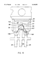
- FIG. 4 is a circuit diagram of the package of FIG. 5.
- FIG. 5 shows a top view of a lead frame in which the MOSFET and Schottky die are interconnected according to a second embodiment of the invention.
- FIG. 6 is a circuit diagram of a buck converter circuit which incorporates the package of the present invention.
- FIGS. 1A and 1B there is shown a known surface mounted T0220 package 10 illustrated in cutaway side and top views, respectively.
- the bottom surface of one or more semiconductor devices 18 is soldered, glued or otherwise attached to a metal plate 14 of the package.
- the plate 14 may also provide thermal contact with the devices as well as an electrical connection.
- Upper, opposing surfaces of the devices are connected to one or more of the lead terminals 12 by wire bonds 16.
- Another of the lead terminals (not shown) may be integral with the plate 14.
- the device 18 and a portion of the lead terminals and plate are encapsulated in a package body, typically formed of resin.
- FIG. 2 shows a top view of a T0220 lead frame 20 upon which a MOSFET 30 and a Schottky diode 32 are co-packaged within a common housing.
- the lead frame 20 is provided with a main pad body 22 from which integral pin 26 extends. Also provided are pins 24 and 28 which are originally integral with the main pad body 22 during molding but are subsequently severed to electrically isolate pins 24 and 28 from one another and from the main pad area 22, as shown in FIG. 1B.
- the lead frame 20 is a conductive lead frame and may have a conventional lead frame solder finish.
- the bottom (cathode) surface of Schottky diode 32 and the bottom (drain) surface of MOSFET 30 are electrically connected to the main pad area 22, such as by a conductive epoxy die attached compound, and are thus connected to pin 26.
- the cathode surface of Schottky diode 22 and the drain surface of MOSFET 30 are soldered to the main pad area 22 or are connected to the main pad area using a conductive glass containing silver particles.
- a top (source) electrode 38 of the MOSFET 30 and the top (anode) electrode 34 of the Schottky diode 32 are wire bonded by bonding wires 42 and 44, respectively, to source pin 28.
- Another top (gate) electrode 36 is wire bonded by bonding wire 46 to the gate pin 24.
- Aluminum bonding wires are most commonly used and the internal bonding extensions of the pins 24 and 28 are typically nickel plated. The bonding wires are generally bonded to the die surface and to the internal bonding extensions using ultrasonic wedge bonding, as is known in the art, though other processes may be used.
- a molded housing as shown in FIGS. 1A and 1B, is formed around the lead frame 20 in a conventional molding operation using an anhydride mold compound such as Dexter Hysol MG15F, though mold compounds such as novolac, biphenol or other compounds may be used.
- anhydride mold compound such as Dexter Hysol MG15F
- mold compounds such as novolac, biphenol or other compounds may be used.
- Other types of housings such as ceramic, hermetic or injection molded metal, may be used.
- the known co-packaged MOSFET and Schottky diode shown in FIG. 2 has the disadvantage that an inductance is present in the wire bond 42 that is located between the anode 34 of the Schottky diode 32 and the extension of the source pin 28.
- This inductance has the undesired effect of slowing down the time needed to sweep out minority carriers from the MOSFET 30 when the MOSFET 30 is shut off and thus the time required for reverse recovery.
- an extra, redundant wire 50 directly connects the anode terminal 34 of the Schottky 32 and the source terminal 38 of the MOSFET 30, as shown in FIG. 3.
- the added wire 50 reduces the inductance present between the source pin and the anode electrode.
- the added wire 50 is a stitch bond.
- FIG. 4 illustrates the circuit formed by the co-packaged vertical conduction MOSFET 30 and the Schottky diode 32 of the invention.
- the drain of the MOSFET 30 is connected to the high side and its source is connected to the low side.
- An inherent body diode 35 is present between the source and drain of the MOSFET 30 and is oriented as shown.
- the Schottky diode is arranged in parallel with and with the same polarity as the body diode 35 so that when the MOSFET 30 is shut off during switching, the lower forward voltage drop Schottky diode 32 provides a fast path for the flow of transient currents caused by minority carriers that are swept out from the MOSFET during reverse recovery.
- FIG. 4 illustrates the circuit formed by the co-packaged vertical conduction MOSFET 30 and the Schottky diode 32 of the invention.
- FIG. 5 shows an alternative embodiment of the invention in which the source terminal 38 of MOSFET 30 and the cathode terminal 34 of Schottky diode 32 are connected by wire bonds 142 and 144, respectively, to isolated pin 28, and the gate terminal 36 of MOSFET 30 is connected by wire bond 146 to pin 24.
- An added wire bond 150 in accordance with the invention, directly connects the source terminal of the MOSFET to the anode terminal of the Schottky diode and shortens the conduction path, thereby reducing the inductance L in the manner shown in FIG. 4.
- MOSFET 30 of FIGS. 3, 4 and 5 may be a 30V, 35 m-ohm die which is available from International Rectifier Corporation.
- FIG. 6 shows an example of a circuit which uses the reduced inductance, co-packaged MOSFET and Schottky diode of the invention.
- a synchronous buck converter circuit uses an N channel MOSFET 200 as the switching device.
- MOSFET 210 and Schottky diode 212 which are co-packaged in housing 230, are arranged in parallel for synchronous rectification.
- the letters D, S, K and A designate the Drain of MOSFET 210; the source of MOSFET 210; the cathode of diode 212 and the anode of diode 212 respectively.
- this arrangement eliminates the effect of the inherent body diode of the vertical conduction MOSFET 210 from the circuit because the Schottky diode 212 handles the reverse current flow seen by the synchronous rectifier during the "wait" state of the controller 240.
- an added wire 220 connects the source of MOSFET 210 directly to the anode of Schottky diode 212 in the manner described above, thereby reducing the inductance present between the anode of Schottky diode 212 and the ground terminal.
Abstract
Description
Claims (18)
Priority Applications (1)
| Application Number | Priority Date | Filing Date | Title |
|---|---|---|---|
| US09/070,097 US6144093A (en) | 1998-04-27 | 1998-04-27 | Commonly housed diverse semiconductor die with reduced inductance |
Applications Claiming Priority (1)
| Application Number | Priority Date | Filing Date | Title |
|---|---|---|---|
| US09/070,097 US6144093A (en) | 1998-04-27 | 1998-04-27 | Commonly housed diverse semiconductor die with reduced inductance |
Publications (1)
| Publication Number | Publication Date |
|---|---|
| US6144093A true US6144093A (en) | 2000-11-07 |
Family
ID=22093108
Family Applications (1)
| Application Number | Title | Priority Date | Filing Date |
|---|---|---|---|
| US09/070,097 Expired - Lifetime US6144093A (en) | 1998-04-27 | 1998-04-27 | Commonly housed diverse semiconductor die with reduced inductance |
Country Status (1)
| Country | Link |
|---|---|
| US (1) | US6144093A (en) |
Cited By (32)
| Publication number | Priority date | Publication date | Assignee | Title |
|---|---|---|---|---|
| US20020033541A1 (en) * | 2000-09-21 | 2002-03-21 | Shotaro Uchida | Semiconductor device manufacturing method and semiconductor device manufactured thereby |
| US6388319B1 (en) * | 1999-05-25 | 2002-05-14 | International Rectifier Corporation | Three commonly housed diverse semiconductor dice |
| US6396127B1 (en) * | 1998-09-25 | 2002-05-28 | International Rectifier Corporation | Semiconductor package |
| US20020125562A1 (en) * | 2000-03-27 | 2002-09-12 | Crowley Sean T. | Attaching semiconductor dies to substrates with conductive straps |
| US6521982B1 (en) * | 2000-06-02 | 2003-02-18 | Amkor Technology, Inc. | Packaging high power integrated circuit devices |
| US20030089980A1 (en) * | 2000-05-08 | 2003-05-15 | Michael Herfurth | Semiconductor component |
| US6566164B1 (en) | 2000-12-07 | 2003-05-20 | Amkor Technology, Inc. | Exposed copper strap in a semiconductor package |
| US6667547B2 (en) * | 1998-05-05 | 2003-12-23 | International Rectifier Corporation | High current capacity semiconductor device package and lead frame with large area connection posts and modified outline |
| US20040041176A1 (en) * | 2002-08-29 | 2004-03-04 | Prall Kirk D. | One F2 memory cell, memory array, related devices and methods |
| US6770982B1 (en) | 2002-01-16 | 2004-08-03 | Marvell International, Ltd. | Semiconductor device power distribution system and method |
| US6791140B2 (en) | 2002-08-08 | 2004-09-14 | Micron Technology, Inc. | Memory transistor structure |
| US20040203206A1 (en) * | 2002-05-01 | 2004-10-14 | Marvell International Ltd. | Flip chip with novel power and ground arrangement |
| US20050151236A1 (en) * | 2003-11-12 | 2005-07-14 | International Rectifier Corporation | Low profile package having multiple die |
| US7050330B2 (en) | 2003-12-16 | 2006-05-23 | Micron Technology, Inc. | Multi-state NROM device |
| WO2006058477A1 (en) * | 2004-11-30 | 2006-06-08 | Alpha & Omega Semiconductor (Shanghai), Ltd. | Thin small outline package in which mosfet and schottky diode being co-packaged |
| US20060118815A1 (en) * | 2004-09-29 | 2006-06-08 | Ralf Otremba | Power semiconductor device |
| US20060124967A1 (en) * | 2003-12-16 | 2006-06-15 | Micron Technology, Inc. | NROM memory cell, memory array, related devices and methods |
| US20070090496A1 (en) * | 2005-10-25 | 2007-04-26 | Ralf Otremba | Electronic module and method of assembling the same |
| US7220634B2 (en) | 2002-06-21 | 2007-05-22 | Micron Technology, Inc. | NROM memory cell, memory array, related devices and methods |
| US7250672B2 (en) * | 2003-11-13 | 2007-07-31 | International Rectifier Corporation | Dual semiconductor die package with reverse lead form |
| US7301235B2 (en) | 2004-06-03 | 2007-11-27 | International Rectifier Corporation | Semiconductor device module with flip chip devices on a common lead frame |
| US20080042143A1 (en) * | 2006-07-26 | 2008-02-21 | Yedinak Joseph A | Avalanche protection for wide bandgap devices |
| US20080191342A1 (en) * | 2007-02-09 | 2008-08-14 | Infineon Technologies Ag | Multi-chip module |
| US20110049580A1 (en) * | 2009-08-28 | 2011-03-03 | Sik Lui | Hybrid Packaged Gate Controlled Semiconductor Switching Device Using GaN MESFET |
| US8258616B1 (en) | 2002-01-16 | 2012-09-04 | Marvell International Ltd. | Semiconductor dice having a shielded area created under bond wires connecting pairs of bonding pads |
| CN103531558A (en) * | 2012-07-02 | 2014-01-22 | 英飞凌科技股份有限公司 | Lead frame packages and methods of formation thereof |
| CN103646942A (en) * | 2010-02-25 | 2014-03-19 | 万国半导体有限公司 | Semiconductor packaging structure applied to power switcher circuit |
| US8896131B2 (en) | 2011-02-03 | 2014-11-25 | Alpha And Omega Semiconductor Incorporated | Cascode scheme for improved device switching behavior |
| JPWO2013046824A1 (en) * | 2011-09-30 | 2015-03-26 | ローム株式会社 | Semiconductor device |
| EP2579443A4 (en) * | 2010-05-27 | 2015-08-05 | Rohm Co Ltd | Electronic circuit |
| US9478484B2 (en) | 2012-10-19 | 2016-10-25 | Infineon Technologies Austria Ag | Semiconductor packages and methods of formation thereof |
| US9536800B2 (en) | 2013-12-07 | 2017-01-03 | Fairchild Semiconductor Corporation | Packaged semiconductor devices and methods of manufacturing |
Citations (6)
| Publication number | Priority date | Publication date | Assignee | Title |
|---|---|---|---|---|
| US5083189A (en) * | 1987-03-31 | 1992-01-21 | Kabushiki Kaisha Toshiba | Resin-sealed type IC device |
| US5084753A (en) * | 1989-01-23 | 1992-01-28 | Analog Devices, Inc. | Packaging for multiple chips on a single leadframe |
| US5200640A (en) * | 1991-08-12 | 1993-04-06 | Electron Power Inc. | Hermetic package having covers and a base providing for direct electrical connection |
| US5332921A (en) * | 1992-04-27 | 1994-07-26 | Kabushiki Kaisha Toshiba | Resin-seal type semiconductor device |
| US5544038A (en) * | 1992-09-21 | 1996-08-06 | General Electric Company | Synchronous rectifier package for high-efficiency operation |
| US5814884A (en) * | 1996-10-24 | 1998-09-29 | International Rectifier Corporation | Commonly housed diverse semiconductor die |
-
1998
- 1998-04-27 US US09/070,097 patent/US6144093A/en not_active Expired - Lifetime
Patent Citations (7)
| Publication number | Priority date | Publication date | Assignee | Title |
|---|---|---|---|---|
| US5083189A (en) * | 1987-03-31 | 1992-01-21 | Kabushiki Kaisha Toshiba | Resin-sealed type IC device |
| US5084753A (en) * | 1989-01-23 | 1992-01-28 | Analog Devices, Inc. | Packaging for multiple chips on a single leadframe |
| US5200640A (en) * | 1991-08-12 | 1993-04-06 | Electron Power Inc. | Hermetic package having covers and a base providing for direct electrical connection |
| US5332921A (en) * | 1992-04-27 | 1994-07-26 | Kabushiki Kaisha Toshiba | Resin-seal type semiconductor device |
| US5544038A (en) * | 1992-09-21 | 1996-08-06 | General Electric Company | Synchronous rectifier package for high-efficiency operation |
| US5814884A (en) * | 1996-10-24 | 1998-09-29 | International Rectifier Corporation | Commonly housed diverse semiconductor die |
| US5814884C1 (en) * | 1996-10-24 | 2002-01-29 | Int Rectifier Corp | Commonly housed diverse semiconductor die |
Cited By (83)
| Publication number | Priority date | Publication date | Assignee | Title |
|---|---|---|---|---|
| US6667547B2 (en) * | 1998-05-05 | 2003-12-23 | International Rectifier Corporation | High current capacity semiconductor device package and lead frame with large area connection posts and modified outline |
| US6396127B1 (en) * | 1998-09-25 | 2002-05-28 | International Rectifier Corporation | Semiconductor package |
| US6388319B1 (en) * | 1999-05-25 | 2002-05-14 | International Rectifier Corporation | Three commonly housed diverse semiconductor dice |
| US6707138B2 (en) | 1999-12-01 | 2004-03-16 | Amkor Technology, Inc. | Semiconductor device including metal strap electrically coupled between semiconductor die and metal leadframe |
| US20020125562A1 (en) * | 2000-03-27 | 2002-09-12 | Crowley Sean T. | Attaching semiconductor dies to substrates with conductive straps |
| US6459147B1 (en) | 2000-03-27 | 2002-10-01 | Amkor Technology, Inc. | Attaching semiconductor dies to substrates with conductive straps |
| US20030089980A1 (en) * | 2000-05-08 | 2003-05-15 | Michael Herfurth | Semiconductor component |
| US6995467B2 (en) * | 2000-05-08 | 2006-02-07 | Infineon Technologies Ag | Semiconductor component |
| US6521982B1 (en) * | 2000-06-02 | 2003-02-18 | Amkor Technology, Inc. | Packaging high power integrated circuit devices |
| US20050121799A1 (en) * | 2000-09-21 | 2005-06-09 | Shotaro Uchida | Semiconductor device manufacturing method and semiconductor device manufactured thereby |
| US20020033541A1 (en) * | 2000-09-21 | 2002-03-21 | Shotaro Uchida | Semiconductor device manufacturing method and semiconductor device manufactured thereby |
| US6919644B2 (en) * | 2000-09-21 | 2005-07-19 | Kabushiki Kaisha Toshiba | Semiconductor device manufacturing method and semiconductor device manufactured thereby |
| US6723582B2 (en) | 2000-12-07 | 2004-04-20 | Amkor Technology, Inc. | Method of making a semiconductor package having exposed metal strap |
| US6566164B1 (en) | 2000-12-07 | 2003-05-20 | Amkor Technology, Inc. | Exposed copper strap in a semiconductor package |
| US6770982B1 (en) | 2002-01-16 | 2004-08-03 | Marvell International, Ltd. | Semiconductor device power distribution system and method |
| US8637975B1 (en) | 2002-01-16 | 2014-01-28 | Marvell International Ltd. | Semiconductor device having lead wires connecting bonding pads formed on opposite sides of a core region forming a shield area |
| US9240372B1 (en) | 2002-01-16 | 2016-01-19 | Marvell International Ltd. | Semiconductor die having lead wires formed over a circuit in a shielded area |
| US6982220B1 (en) | 2002-01-16 | 2006-01-03 | Marvell International Ltd. | Semiconductor device power distribution system and method |
| US8258616B1 (en) | 2002-01-16 | 2012-09-04 | Marvell International Ltd. | Semiconductor dice having a shielded area created under bond wires connecting pairs of bonding pads |
| US20040203206A1 (en) * | 2002-05-01 | 2004-10-14 | Marvell International Ltd. | Flip chip with novel power and ground arrangement |
| US6890794B2 (en) | 2002-05-01 | 2005-05-10 | Marvell Semiconductor Israel Ltd. | Flip chip with novel power and ground arrangement |
| US6861762B1 (en) | 2002-05-01 | 2005-03-01 | Marvell Semiconductor Israel Ltd. | Flip chip with novel power and ground arrangement |
| US7220634B2 (en) | 2002-06-21 | 2007-05-22 | Micron Technology, Inc. | NROM memory cell, memory array, related devices and methods |
| US8441056B2 (en) | 2002-06-21 | 2013-05-14 | Micron Technology, Inc. | NROM memory cell, memory array, related devices and methods |
| US7541242B2 (en) | 2002-06-21 | 2009-06-02 | Micron Technology, Inc. | NROM memory cell, memory array, related devices and methods |
| US7535048B2 (en) | 2002-06-21 | 2009-05-19 | Micron Technology, Inc. | NROM memory cell, memory array, related devices and methods |
| US20050122787A1 (en) * | 2002-08-08 | 2005-06-09 | Prall Kirk D. | Memory transistor and methods |
| US20070111443A1 (en) * | 2002-08-08 | 2007-05-17 | Prall Kirk D | Memory transistor and methods |
| US7745283B2 (en) | 2002-08-08 | 2010-06-29 | Micron Technology, Inc. | Method of fabricating memory transistor |
| US7651911B2 (en) | 2002-08-08 | 2010-01-26 | Micron Technology, Inc. | Memory transistor and methods |
| US6835619B2 (en) | 2002-08-08 | 2004-12-28 | Micron Technology, Inc. | Method of forming a memory transistor comprising a Schottky contact |
| US6791140B2 (en) | 2002-08-08 | 2004-09-14 | Micron Technology, Inc. | Memory transistor structure |
| US20040041176A1 (en) * | 2002-08-29 | 2004-03-04 | Prall Kirk D. | One F2 memory cell, memory array, related devices and methods |
| US7095099B2 (en) * | 2003-11-12 | 2006-08-22 | International Rectifier Corporation | Low profile package having multiple die |
| US20050151236A1 (en) * | 2003-11-12 | 2005-07-14 | International Rectifier Corporation | Low profile package having multiple die |
| US7250672B2 (en) * | 2003-11-13 | 2007-07-31 | International Rectifier Corporation | Dual semiconductor die package with reverse lead form |
| US20060124967A1 (en) * | 2003-12-16 | 2006-06-15 | Micron Technology, Inc. | NROM memory cell, memory array, related devices and methods |
| US7050330B2 (en) | 2003-12-16 | 2006-05-23 | Micron Technology, Inc. | Multi-state NROM device |
| US7269072B2 (en) | 2003-12-16 | 2007-09-11 | Micron Technology, Inc. | NROM memory cell, memory array, related devices and methods |
| US7371642B2 (en) | 2003-12-16 | 2008-05-13 | Micron Technology, Inc. | Multi-state NROM device |
| US7750389B2 (en) | 2003-12-16 | 2010-07-06 | Micron Technology, Inc. | NROM memory cell, memory array, related devices and methods |
| US7238599B2 (en) | 2003-12-16 | 2007-07-03 | Micron Technology, Inc. | Multi-state NROM device |
| US7301804B2 (en) | 2003-12-16 | 2007-11-27 | Micro Technology, Inc. | NROM memory cell, memory array, related devices and methods |
| US7269071B2 (en) | 2003-12-16 | 2007-09-11 | Micron Technology, Inc. | NROM memory cell, memory array, related devices and methods |
| US7301235B2 (en) | 2004-06-03 | 2007-11-27 | International Rectifier Corporation | Semiconductor device module with flip chip devices on a common lead frame |
| US7514778B2 (en) * | 2004-09-29 | 2009-04-07 | Infineon Technologies Ag | Power semiconductor device |
| US20060118815A1 (en) * | 2004-09-29 | 2006-06-08 | Ralf Otremba | Power semiconductor device |
| CN100359686C (en) * | 2004-11-30 | 2008-01-02 | 万代半导体元件(上海)有限公司 | Thin and small outer shape package combined by metal oxide semiconductor field effect transistor and schottky diode |
| US8089139B2 (en) | 2004-11-30 | 2012-01-03 | Alpha & Omega Semiconductor, Ltd. | Small outline package in which MOSFET and Schottky diode being co-packaged |
| US20080197458A1 (en) * | 2004-11-30 | 2008-08-21 | Zhenyu Shi | Small Outline Package in Which Mosfet and Schottky Diode Being Co-Packaged |
| WO2006058477A1 (en) * | 2004-11-30 | 2006-06-08 | Alpha & Omega Semiconductor (Shanghai), Ltd. | Thin small outline package in which mosfet and schottky diode being co-packaged |
| US7443014B2 (en) | 2005-10-25 | 2008-10-28 | Infineon Technologies Ag | Electronic module and method of assembling the same |
| DE102006050291B4 (en) * | 2005-10-25 | 2015-04-02 | Infineon Technologies Ag | Electronic assembly and method to populate them |
| US20070090496A1 (en) * | 2005-10-25 | 2007-04-26 | Ralf Otremba | Electronic module and method of assembling the same |
| US20110089432A1 (en) * | 2006-07-26 | 2011-04-21 | Fairchild Semiconductor Corporation | Wide bandgap device in parallel with a device that has a lower avalanche breakdown voltage and a higher forward voltage drop than the wide bandgap device |
| US7859057B2 (en) * | 2006-07-26 | 2010-12-28 | Fairchild Semiconductor Corporation | Wide bandgap device in parallel with a device that has a lower avalanche breakdown voltage and a higher forward voltage drop than the wide bandgap device |
| US8357976B2 (en) | 2006-07-26 | 2013-01-22 | Fairchild Semiconductor Corporation | Wide bandgap device in parallel with a device that has a lower avalanche breakdown voltage and a higher forward voltage drop than the wide bandgap device |
| US7586156B2 (en) | 2006-07-26 | 2009-09-08 | Fairchild Semiconductor Corporation | Wide bandgap device in parallel with a device that has a lower avalanche breakdown voltage and a higher forward voltage drop than the wide bandgap device |
| DE112007001762T5 (en) | 2006-07-26 | 2009-05-28 | Fairchild Semiconductor Corp. | Avalanche protection for wide bandgap devices |
| US20080042143A1 (en) * | 2006-07-26 | 2008-02-21 | Yedinak Joseph A | Avalanche protection for wide bandgap devices |
| US20080191342A1 (en) * | 2007-02-09 | 2008-08-14 | Infineon Technologies Ag | Multi-chip module |
| US8188596B2 (en) * | 2007-02-09 | 2012-05-29 | Infineon Technologies Ag | Multi-chip module |
| US20110049580A1 (en) * | 2009-08-28 | 2011-03-03 | Sik Lui | Hybrid Packaged Gate Controlled Semiconductor Switching Device Using GaN MESFET |
| CN103646942A (en) * | 2010-02-25 | 2014-03-19 | 万国半导体有限公司 | Semiconductor packaging structure applied to power switcher circuit |
| CN103646942B (en) * | 2010-02-25 | 2016-01-13 | 万国半导体有限公司 | A kind of semiconductor package being applied to power switcher circuit |
| US9245956B2 (en) | 2010-05-27 | 2016-01-26 | Rohm Co., Ltd. | Electronic circuit comprising unipolar and bipolar devices |
| US9679877B2 (en) | 2010-05-27 | 2017-06-13 | Rohm Co., Ltd. | Semiconductor device comprising PN junction diode and Schottky barrier diode |
| US11894349B2 (en) | 2010-05-27 | 2024-02-06 | Rohm Co., Ltd. | Semiconductor device comprising PN junction diode and Schottky barrier diode |
| US11502063B2 (en) | 2010-05-27 | 2022-11-15 | Rohm Co., Ltd. | Semiconductor device comprising PN junction diode and Schottky barrier diode |
| EP3813247A1 (en) * | 2010-05-27 | 2021-04-28 | Rohm Co., Ltd. | Electronic module |
| US9461021B2 (en) | 2010-05-27 | 2016-10-04 | Rohm Co., Ltd. | Electronic circuit comprising PN junction and schottky barrier diodes |
| US10896896B2 (en) | 2010-05-27 | 2021-01-19 | Rohm Co., Ltd. | Semiconductor device comprising PN junction diode and schottky barrier diode |
| US10559552B2 (en) | 2010-05-27 | 2020-02-11 | Rohm Co., Ltd. | Semiconductor device comprising PN junction diode and Schottky barrier diode |
| EP3528380A1 (en) * | 2010-05-27 | 2019-08-21 | Rohm Co., Ltd. | Electronic circuit |
| EP2579443A4 (en) * | 2010-05-27 | 2015-08-05 | Rohm Co Ltd | Electronic circuit |
| US9917074B2 (en) | 2010-05-27 | 2018-03-13 | Rohm Co., Ltd. | Semiconductor device comprising PN junction diode and schottky barrier diode |
| US10074634B2 (en) | 2010-05-27 | 2018-09-11 | Rohm Co., Ltd. | Semiconductor device comprising PN junction diode and schottky barrier diode |
| US8896131B2 (en) | 2011-02-03 | 2014-11-25 | Alpha And Omega Semiconductor Incorporated | Cascode scheme for improved device switching behavior |
| JPWO2013046824A1 (en) * | 2011-09-30 | 2015-03-26 | ローム株式会社 | Semiconductor device |
| DE102013106932B4 (en) * | 2012-07-02 | 2017-06-01 | Infineon Technologies Ag | Leadframe housing and method for its manufacture |
| CN103531558A (en) * | 2012-07-02 | 2014-01-22 | 英飞凌科技股份有限公司 | Lead frame packages and methods of formation thereof |
| US9478484B2 (en) | 2012-10-19 | 2016-10-25 | Infineon Technologies Austria Ag | Semiconductor packages and methods of formation thereof |
| US9536800B2 (en) | 2013-12-07 | 2017-01-03 | Fairchild Semiconductor Corporation | Packaged semiconductor devices and methods of manufacturing |
Similar Documents
| Publication | Publication Date | Title |
|---|---|---|
| US6144093A (en) | Commonly housed diverse semiconductor die with reduced inductance | |
| US7443014B2 (en) | Electronic module and method of assembling the same | |
| US8629467B2 (en) | Semiconductor device | |
| US10204899B2 (en) | Semiconductor device with first and second chips and connections thereof and a manufacturing method of the same | |
| US6297552B1 (en) | Commonly housed diverse semiconductor die | |
| US6448643B2 (en) | Three commonly housed diverse semiconductor dice | |
| US5977630A (en) | Plural semiconductor die housed in common package with split heat sink | |
| US8345458B2 (en) | Semiconductor device | |
| US7227198B2 (en) | Half-bridge package | |
| US20240014193A1 (en) | Semiconductor device | |
| US6388319B1 (en) | Three commonly housed diverse semiconductor dice | |
| JP3583382B2 (en) | Semiconductor die mounting structure |
Legal Events
| Date | Code | Title | Description |
|---|---|---|---|
| AS | Assignment |
Owner name: INTERNATIONAL RECTIFIER CORPORATION, CALIFORNIA Free format text: ASSIGNMENT OF ASSIGNORS INTEREST;ASSIGNORS:DAVIS, CHRISTOPHER;CONNAH, GLYNN;REEL/FRAME:009153/0172;SIGNING DATES FROM 19980417 TO 19980422 |
|
| AS | Assignment |
Owner name: BANQUE NATIONALE DE PARIS, CALIFORNIA Free format text: SECURITY INTEREST;ASSIGNOR:INTERNATIONAL RECTIFIER CORP.;REEL/FRAME:010070/0701 Effective date: 19990711 |
|
| STCF | Information on status: patent grant |
Free format text: PATENTED CASE |
|
| FPAY | Fee payment |
Year of fee payment: 4 |
|
| FPAY | Fee payment |
Year of fee payment: 8 |
|
| FEPP | Fee payment procedure |
Free format text: PAYOR NUMBER ASSIGNED (ORIGINAL EVENT CODE: ASPN); ENTITY STATUS OF PATENT OWNER: LARGE ENTITY |
|
| FPAY | Fee payment |
Year of fee payment: 12 |
|
| AS | Assignment |
Owner name: INTERNATIONAL RECTIFIER CORPORATION, CALIFORNIA Free format text: RELEASE BY SECURED PARTY;ASSIGNOR:BNP PARIBAS (FORMERLY KNOWN AS BANQUE NATIONALE DE PARIS);REEL/FRAME:028315/0386 Effective date: 20110128 |
|
| AS | Assignment |
Owner name: GLOBAL LED SOLUTIONS, LLC, VIRGINIA Free format text: ASSIGNMENT OF ASSIGNORS INTEREST;ASSIGNOR:INTERNATIONAL RECTIFIER CORPORATION;REEL/FRAME:029034/0162 Effective date: 20120824 |
|
| AS | Assignment |
Owner name: INTELLECTUAL DISCOVERY CO., LTD., KOREA, REPUBLIC Free format text: ASSIGNMENT OF ASSIGNORS INTEREST;ASSIGNOR:GLOBAL LED SOLUTIONS, LLC;REEL/FRAME:034292/0501 Effective date: 20141126 |