US6144218A - High speed analog compensated input buffer - Google Patents
High speed analog compensated input buffer Download PDFInfo
- Publication number
- US6144218A US6144218A US09/012,201 US1220198A US6144218A US 6144218 A US6144218 A US 6144218A US 1220198 A US1220198 A US 1220198A US 6144218 A US6144218 A US 6144218A
- Authority
- US
- United States
- Prior art keywords
- logic
- signal
- transistor
- pvt
- current source
- Prior art date
- Legal status (The legal status is an assumption and is not a legal conclusion. Google has not performed a legal analysis and makes no representation as to the accuracy of the status listed.)
- Expired - Lifetime
Links
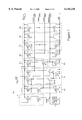
Images


Classifications
-
- H—ELECTRICITY
- H03—ELECTRONIC CIRCUITRY
- H03K—PULSE TECHNIQUE
- H03K19/00—Logic circuits, i.e. having at least two inputs acting on one output; Inverting circuits
- H03K19/003—Modifications for increasing the reliability for protection
- H03K19/00369—Modifications for compensating variations of temperature, supply voltage or other physical parameters
- H03K19/00384—Modifications for compensating variations of temperature, supply voltage or other physical parameters in field effect transistor circuits
Definitions
- This invention relates to the field of integrated circuits.
- this invention is drawn to analog compensated integrated circuit input/output circuitry.
- I/O timing parameters can severely impact I/O performance, particularly with respect to high performance or high frequency I/O design.
- an I/O circuit e.g., a buffer
- an I/O circuit is designed for operation within strict timing guidelines. Failure to operate with the intended timing parameters may prevent the buffer from operating properly. Alternatively, failure to operate within these timing parameters may prevent the buffer from interfacing properly with other circuitry that does adhere to the timing parameters.
- Variations in temperature may cause the buffer circuitry to operate outside of the intended timing parameters. Process variations introduced during manufacture of the buffer circuitry can cause variations that detract from optimal performance even if the buffer circuitry is still operating within intended timing parameters.
- the buffer circuitry is typically designed to operate at specific voltages or within specified voltage ranges. In practice, however, the voltages are typically within some tolerance factor of the specified voltage or range. Changes in voltage, however, tend to cause a shift in the actual timing parameters of the buffer circuitry.
- the collective effect of process, voltage, and temperature (PVT) variations may prevent the buffer from functioning or prevent the buffer from performing in accordance with the intended timing parameters. Lack of adequate compensation for individual I/O components can result in departure from optimal performance if, for example, the timing parameters change.
- PVT process, voltage, and temperature
- I/O circuitry must translate one type of logic to another type of logic.
- an integrated circuit may have Gunning Transceiver Logic (GTL) based I/O buffers with a complementary metal oxide semiconductor (CMOS) logic based core.
- GTL Gunning Transceiver Logic
- CMOS complementary metal oxide semiconductor
- the I/O circuitry must be able to translate between GTL and CMOS levels in order to properly function. PVT variations within the GTL circuitry or the CMOS circuitry separately or collectively can produce timing parameter changes that prevent the I/O circuitry from operating at optimal performance levels.
- an analog process ⁇ voltage ⁇ temperature (PVT) compensated buffer apparatus includes a differential amplifier providing a first output signal indicative of a difference between an input signal and a reference signal.
- the input signal is compatible with a first type of logic.
- An active gain stage is coupled to translate the first output signal to a second output signal.
- the second output signal is compatible with a second type of logic.
- the differential amplifier and the active gain stage are coupled to receive a process/voltage/temperature (PVT) compensation signal.
- the first type of logic is Gunning Transceiver Logic (GTL) and the second type of logic is complementary metal oxide semiconductor (CMOS) logic.
- GTL Gunning Transceiver Logic
- CMOS complementary metal oxide semiconductor
- FIG. 1 illustrates analog compensation circuitry for providing PVT bias compensation signals to integrated circuit I/O circuitry.
- FIG. 2 illustrates a simplified view of the analog compensation circuitry of FIG. 1.
- FIG. 3 illustrates a GTL input buffer
- FIG. 4 illustrates a GTL input buffer with PVT bias compensation.
- FIG. 5 illustrates a GTL output buffer
- FIG. 6 illustrates a GTL output buffer with PVT bias compensation.
- FIG. 7 illustrates a CMOS output buffer
- FIG. 8 illustrates a CMOS output buffer with PVT bias compensation.
- FIG. 1 illustrates an analog compensation circuit for providing process/voltage/temperature (PVT) bias compensation signals to multiple types of logic within an integrated circuit.
- analog compensation circuit 100 provides PVT bias compensation signals for Gunning Transceiver Logic (GTL) and complementary metal oxide semiconductor (CMOS) logic.
- GTL Gunning Transceiver Logic
- CMOS complementary metal oxide semiconductor
- compensation circuitry 100 can be divided into individual modules for analysis.
- the compensation circuitry includes a first current source 110, a voltage divider 120, a differential amplifier 130, and a second current source 140.
- the compensation circuitry includes logic level converters 160 and 170 to produce PVT bias compensation signals for a second type of logic from the bias compensation signals generated for a first type of logic.
- the first type of logic is GTL and the second type of logic is CMOS logic.
- compensation circuitry 100 includes capacitive elements T17, T18, T19, and T20 to reduce the effect of noise on the compensation circuitry, to reduce the noise in the generated bias compensation signals themselves, and to correlate the output noise with noise already present in the power supply.
- FIG. 2 illustrates another view of analog compensation circuit 100 as analog compensation circuit 200.
- the transistor substrate connections and many of the FIG. 1 reference characters have been eliminated from the illustration in order to more clearly present the analog compensation circuitry.
- transistors T1 and T2 form the first current source 110.
- the first current source is coupled to a precision resistor 116 in order to produce a first reference voltage 118.
- the compensation circuitry excluding the precision resistor 116 resides within an integrated circuit.
- the precision resistor is an external component that can be connected to the first current source 110 using a pin of the integrated circuit.
- Transistors T3 and T4 form voltage divider 120.
- the voltage divider provides a current source bias, VCSB 122, to transistor T2 of the first current source 110.
- voltage divider 120 is designed such that the current source bias 122 is halfway between Vcc and Vss ##EQU1##
- Transistors T5, T6, T7, T8, and T9 form differential amplifier 130.
- Differential amplifier 130 receives the first reference voltage 118 and a second reference voltage 138.
- the second reference voltage 138 is a GTL reference voltage as described in the Gunning Transceiver Logic (GTL) Low-Level High-Speed Interface Standard for Digital Integrated Circuits set forth in JEDEC Std. No. 8-3 (from JEDEC Council Ballot, JCB-93-11A).
- GTL defines minimum high-level and maximum low-level input voltages with respect to reference voltage V REF .
- Input circuitry typically includes a comparator stage operating about a nominal V REF of 0.8 V.
- Output requirements provide for both an open-drain output stage (requiring external termination) and an active pull-up, active pull-down output stage requiring no external termination.
- V REF maximum and minimums are defined as 2/3 of a supply (or termination) voltage less 2%. The supply voltage ranges from approximately 1.14 to 1.26. Thus V REF ranges from 0.74 V to 0.82 V.
- V REF is generated external to the integrated circuit and provided to the integrated circuit through a pin.
- V REF is generated within the integrated circuit. In either embodiment, V REF tracks the supply voltage.
- Variations of the GTL standard include GTL+ which has a nominal V REF of 1.0 V. GTL is described in U.S. Pat. No. 5,023,488.
- Differential amplifier 130 generates the first bias compensation signal VPBIASG 190 in accordance with the result of comparing the first and second reference voltages.
- the first bias compensation signal 190 is coupled to the gate of transistor T1 for feedback control of the first current source 110.
- the first bias compensation signal is a GTL "p-type" transistor bias compensation signal.
- the compensation circuit 100 effectively generates the bias voltage 190 necessary to compensate p-type transistor T1 of the first current source for PVT variations that cause the first voltage reference 118 to vary from the GTL input voltage reference 138.
- the first bias compensation signal, VPBIASG 190 may similarly be applied to control "p-type" current sources in order to achieve operation substantially independent of PVT variations.
- Transistors T10 and T11 form the second current source 140.
- the first bias compensation signal 190 is coupled to the gate of transistor T10 for feedback control of the second current source.
- the current source bias 122 is applied to transistor T11.
- Second current source 140 is coupled to a second load 150.
- the voltage developed across second load 150 is the second bias compensation signal VNBIASG 196.
- the second bias compensation signal is a GTL "n-type" transistor bias compensation signal.
- capacitive elements are included in the circuit in order to ensure a high correlation between any power supply noise and the first and second bias compensation signals. These capacitive elements are included to capacitively couple the bias compensation signals to one of Vcc or Vss.
- transistors T17 and T18 capacitively couple the first and second bias compensation signals to one of Vcc or Vss.
- transistor T17 capacitively couples the first bias compensation signal 190 to Vcc.
- transistor T18 capacitively couples the second bias compensation signal 196 to Vss.
- Transistors T17 and T18 collectively form a first set 180 of low pass filters.
- capacitive elements serve to reduce the frequency response of the compensation circuit so that high frequency noise in the first and second reference signals (118, 138) do not appreciably affect the operation of the compensation circuit.
- the capacitive elements also tend to reduce the amount of noise present in the first and second bias compensation signals.
- the capacitive elements also force the bias compensation signals to track the power supply noise (i.e., the capacitive elements ensure correlation between power supply noise and noise in bias compensation signals).
- transistor T17 ensures that the first bias compensation 190 signal tracks Vcc.
- Transistor T18 ensures that the second bias compensation signal 196 tracks Vss. In an alternative embodiment, no such capacitive elements are included.
- the compensation circuitry provides PVT compensation signals to mixed types of logic.
- an integrated circuit may include GTL and CMOS logic. Each type of logic will require PVT compensation to ensure optimal performance.
- Logic level bias converters 160 and 170 permit compensation circuit 100 to provide PVT bias compensation signals for a second type of logic from the bias compensation signals generated for a first type of logic.
- the first logic level bias converter 160 generates a CMOS "n-type” bias compensation signal 194 from the GTL "p-type” bias compensation signal 190.
- the second logic level bias converter 170 generates a CMOS "p-type” bias compensation signal 192 from the GTL "n-type” bias compensation signal 196.
- Transistors T13 and T14 form the first logic level bias converter 160.
- Transistor T13 is coupled to Vcc to provide current to diode connected transistor T14.
- the gate of transistor T13 is biased by the first bias compensation signal 190.
- Transistor T14 is coupled to transistor T13 and Vss.
- the voltage developed across T14 serves as a third compensation signal.
- the third bias compensation signal is a CMOS "n-type" bias compensation signal designated VNBIAS 194.
- Transistors T15 and T16 form the second logic level bias converter.
- Transistor T16 is coupled to Vss to provide current to diode connected transistor T15.
- the gate of transistor T16 is biased by the second bias compensation signal 196.
- Transistor T15 is coupled to transistor T16 and Vcc.
- the voltage developed across T15 serves as a fourth compensation signal.
- the fourth compensation signal is a CMOS "p-type" bias compensation signal designated VPBIAS 192.
- Transistor T19 capacitively couples the third bias compensation signal 194 to Vcc.
- Transistor T20 capacitively couples the fourth bias compensation signal 192 to Vss.
- Transistors T19 and T20 collectively form a second set 182 of low pass filters. The presence of these capacitive elements tends to reduce the effects of high frequency noise within the compensation circuitry. The capacitive elements tend to reduce the amount of noise in the third and fourth bias compensation signals. The capacitive coupling also ensures a high correlation between on die power supply noise and the third and fourth compensation signals.
- compensation circuitry 100 comprises metal oxide semiconductor (MOS) transistors.
- MOS metal oxide semiconductor
- transistors T1, T2, T3, T4, T5, T6, T10, T11, T13, T15, T17, and T19 are PMOS transistors.
- Transistors T7, T8, T9, T12, T14, T16, T18, and T20 are NMOS transistors.
- complementary types are used, thus PMOS transistors are substituted for the NMOS transistors and NMOS transistors are substituted for the PMOS transistors.
- the use of complementary types requires switching Vcc and Vss.
- the bias compensation signal pairs (190, 196 and 192, 194) will similarly have their types (i.e., "p", or "n") switched from those illustrated in FIG. 1.
- FIG. 3 illustrates a typical GTL input buffer 300.
- Input buffer 300 is designed to translate a GTL-compatible input signal 310 into a CMOS-compatible signal 342.
- Input buffer 300 is susceptible to PVT variations.
- FIG. 4 illustrates GTL input buffer 400.
- Input buffer 400 translates a GTL-compatible input signal 410 into a CMOS-compatible signal 442.
- Input buffer 400 is designed to receive an analog PVT bias compensation signal.
- bias compensation signals such as VPBIASG 190 of FIG. 1 is applied to the current sources used to control the functioning of GTL input buffer 400.
- GTL input buffer 400 includes a differential amplifier 430 and an active gain stage 440.
- Transistors T1, T2, T3, T4, and T5 form the differential amplifier 430.
- Transistors T6 and T7 form the active gain stage 440.
- GTL input buffer 400 is fabricated within an integrated circuit.
- Differential amplifier 430 receives the GTL-compatible input signal 410 and a GTL input reference voltage 434 as previously described. Differential amplifier 430 effectively acts as a comparator to provide an output signal 436 reflecting the relationship between GTL input voltage reference signal 434 and GTL input signal 410. Differential amplifier 430 includes an active current mirror load (T4, T5), differential input devices (T2, T3), and a current source (T1).
- T4, T5 active current mirror load
- T2, T3 differential input devices
- T1 current source
- the gate of transistor T2 receives the GTL input signal 410.
- the gate of transistor T3 receives the GTL voltage reference signal 434.
- the differential input transistors are coupled to the active current load transistors at nodes 450 and 451.
- Non-inverting output signal 436 is selected from node 451.
- Transistor T1 is designed to operate as a current source for differential amplifier 430. Without adequate PVT compensation, T1's operating parameters can drift such that T1 is not operating independently of PVT variations.
- transistor T1 is a p-type transistor. Transistor T1 is therefore biased by PVT compensation signal VPBIASG 190. Given that the compensation circuitry 100 and the input buffer circuitry are fabricated on the same die, the PVT compensation signal VPBIASG 190 causes transistor T1 to behave as a constant current source substantially independent of PVT variations.
- the differential amplifier output signal 436 is not fully CMOS compatible. Differential amplifier output signal 436 is provided to active gain stage 440 in order generate CMOS compatible logic levels.
- Active gain inverting output stage 440 includes transistors T6 and T7.
- Transistor T6 acts as a current source.
- the first bias compensation signal (VPBIASG 190) is coupled to the gate of transistor T6 in order to compensate for fluctuations due to PVT variations.
- Output signal 436 is coupled to the gate of transistor T7.
- the resulting input buffer output signal 442 is CMOS compatible. In one embodiment, the output signal 442 is routed to integrated circuit CMOS logic residing on a same die as GTL input buffer 400.
- GTL input buffer 400 comprises metal oxide semiconductor (MOS) transistors.
- MOS metal oxide semiconductor
- transistors T1, T3, and T6 are PMOS transistors.
- Transistors T4, T5, and T7 are NMOS transistors.
- FIG. 5 illustrates a typical GTL output buffer 500.
- GTL output buffer 500 includes transistors T1, T2, T3, T4, and T5.
- GTL output buffer 500 receives a CMOS compatible input signal 510 and translates it to a GTL compatible output signal 542.
- GTL output buffer 500 is susceptible to PVT variations.
- FIG. 6 illustrates a GTL output buffer 600.
- Output buffer 600 is designed to receive an analog PVT bias compensation signal.
- Output buffer 600 includes transistors T1, T2, T3, T4, T5, T6, and T7.
- PVT bias compensation signals VPBIASG 190 and VNBIASG 196 of FIG. 1 are applied to current control devices T6 and T7 in order to produce PVT compensated GTL compatible output signal 642.
- FIG. 7 illustrates a typical CMOS output buffer 700.
- CMOS output buffer 700 includes transistors T1, T2, T3, T4, T5, T6, T7, and T8.
- CMOS output buffer 700 receives a CMOS compatible input signal 710 and provides a buffered CMOS compatible output signal 742.
- CMOS output buffer 700 is susceptible to PVT variations.
- FIG. 8 illustrates CMOS output buffer 800 with PVT bias compensation.
- Output buffer 800 is designed to receive analog PVT bias compensation signals.
- CMOS output buffer 800 includes transistors T9, T10, T11, and T12 for PVT bias compensation.
- CMOS PVT bias compensation VPBIAS 192 is applied to the gates of PMOS transistors T9 and T11 of FIG. 8.
- CMOS PVT bias compensation VNBIAS 194 is applied to the gates of NMOS transistors T10 and T12 of FIG. 8.
- CMOS output buffer 800 provides a PVT compensated CMOS output signal 842.
- the compensation circuitry 100 can be modified to account for other pairs of logic families (e.g., GTL+, CMOS). With only 20 transistors, compensation circuitry 100 provides PVT compensation bias signal pairs for two logic families. Moreover, the compensation circuitry includes low pass filters to minimize the effect of noise on the compensation circuitry as well as to minimize the amount of noise in the compensation bias signals. If compensation for only one type of logic family is necessary the bias logic level converters (160, 170) and associated capacitive elements (T19, T20) can be eliminated to provide compensation circuitry with even fewer components.
- VPBIASG 190 When implementing the analog compensation circuit 100 in an integrated circuit, some of the functional units can be implemented locally. This may be particularly useful in an integrated circuit having mixed logic families.
- the remaining filters and logic level bias translators e.g., 160, 170, and 182
- the integrated circuit designer may bus one bias signal (e.g., VPBIASG 190) or perhaps two (i.e., VPBIASG 190, VNBIASG 196) rather than four bias signals around the integrated circuit die.
- the integrated circuit includes a GTL portion and a CMOS portion.
- the GTL portion includes current source 110, voltage divider 120, differential amplifier 130, second current source 140, second load 150, and filter 180.
- the CMOS portion includes logic level bias converters 160, 170, and filter 182.
- VPBIASG 190 and VNBIASG 196 are then bussed to the CMOS portion in order to generate the CMOS bias signals VPBIAS 192, and VNBIAS 194 locally within the CMOS portion. This may be particularly useful for an integrated circuit having islands of different logic family types.
Abstract
Description
Claims (19)
Priority Applications (1)
| Application Number | Priority Date | Filing Date | Title |
|---|---|---|---|
| US09/012,201 US6144218A (en) | 1998-01-23 | 1998-01-23 | High speed analog compensated input buffer |
Applications Claiming Priority (1)
| Application Number | Priority Date | Filing Date | Title |
|---|---|---|---|
| US09/012,201 US6144218A (en) | 1998-01-23 | 1998-01-23 | High speed analog compensated input buffer |
Publications (1)
| Publication Number | Publication Date |
|---|---|
| US6144218A true US6144218A (en) | 2000-11-07 |
Family
ID=21753833
Family Applications (1)
| Application Number | Title | Priority Date | Filing Date |
|---|---|---|---|
| US09/012,201 Expired - Lifetime US6144218A (en) | 1998-01-23 | 1998-01-23 | High speed analog compensated input buffer |
Country Status (1)
| Country | Link |
|---|---|
| US (1) | US6144218A (en) |
Cited By (11)
| Publication number | Priority date | Publication date | Assignee | Title |
|---|---|---|---|---|
| US6404223B1 (en) * | 2001-01-22 | 2002-06-11 | Mayo Foundation For Medical Education And Research | Self-terminating current mirror transceiver logic |
| US6556022B2 (en) | 2001-06-29 | 2003-04-29 | Intel Corporation | Method and apparatus for local parameter variation compensation |
| US6556049B2 (en) * | 2000-08-21 | 2003-04-29 | Samsung Electronics, Co., Ltd. | Output driver having output current compensation and method of compensating output current |
| US20030122572A1 (en) * | 2002-01-02 | 2003-07-03 | Broadcom Corporation | Methods and systems for sensing and compensating for process, voltage, temperature, and load variations |
| US6633178B2 (en) | 2001-09-28 | 2003-10-14 | Intel Corporation | Apparatus and method for power efficient line driver |
| US6686774B1 (en) * | 2001-07-19 | 2004-02-03 | Raza Microelectronics, Inc. | System and method for a high speed, bi-directional, zero turnaround time, pseudo differential bus capable of supporting arbitrary number of drivers and receivers |
| US20040059845A1 (en) * | 2002-09-25 | 2004-03-25 | Samsung Electronics Co., Ltd. | Simultaneous bidirectional input/output circuit |
| US20050185480A1 (en) * | 2004-02-19 | 2005-08-25 | Anoop Mukker | Dynamically activated memory controller data termination |
| US20080224774A1 (en) * | 2005-09-26 | 2008-09-18 | Silicon Storage Technology, Inc. | Method and Apparatus for Systematic and Random Variation and Mismatch Compensation for Multilevel Flash Memory Operation |
| US20130106504A1 (en) * | 2011-10-27 | 2013-05-02 | Taiwan Semiconductor Manufacturing Company, Ltd. | Integrated circuits with cascode transistor |
| CN104808729A (en) * | 2014-01-27 | 2015-07-29 | 澜起科技(上海)有限公司 | Voltage stabilizer and voltage stabilizing method |
Citations (11)
| Publication number | Priority date | Publication date | Assignee | Title |
|---|---|---|---|---|
| US4847522A (en) * | 1988-06-08 | 1989-07-11 | Maxim Integrated Products | CMOS amplifier/driver stage with output disable feature |
| US5268872A (en) * | 1990-09-28 | 1993-12-07 | Kabushiki Kaisha Toshiba | Semiconductor integrated circuit capable of compensating errors in manufacturing process |
| US5483184A (en) * | 1993-06-08 | 1996-01-09 | National Semiconductor Corporation | Programmable CMOS bus and transmission line receiver |
| US5604448A (en) * | 1994-09-09 | 1997-02-18 | Hyundai Electronics Industries Co., Ltd. | Output buffer circuit having low noise characteristics |
| US5656952A (en) * | 1995-11-13 | 1997-08-12 | Analog Devices, Inc. | All-MOS differential high speed output driver for providing positive-ECL levels into a variable load impedance |
| US5736871A (en) * | 1995-02-28 | 1998-04-07 | Nec Corporation | Differential pair input buffer circuit with a variable current source |
| US5847581A (en) * | 1996-12-31 | 1998-12-08 | Intel Corporation | Low power CMOS precision input receiver with integrated reference |
| US5900745A (en) * | 1995-07-28 | 1999-05-04 | Nec Corporation | Semiconductor device including input buffer circuit capable of amplifying input signal with low amplitude in high speed and under low current consumption |
| US5910736A (en) * | 1995-10-17 | 1999-06-08 | Denso Corporation | Differential-type data transmitter |
| US5936428A (en) * | 1995-05-10 | 1999-08-10 | Micron Technology, Inc. | Low power, high speed level shifter |
| US6025792A (en) * | 1998-01-23 | 2000-02-15 | Intel Corporation | Analog compensation circuitry for integrated circuit input/output circuitry |
-
1998
- 1998-01-23 US US09/012,201 patent/US6144218A/en not_active Expired - Lifetime
Patent Citations (11)
| Publication number | Priority date | Publication date | Assignee | Title |
|---|---|---|---|---|
| US4847522A (en) * | 1988-06-08 | 1989-07-11 | Maxim Integrated Products | CMOS amplifier/driver stage with output disable feature |
| US5268872A (en) * | 1990-09-28 | 1993-12-07 | Kabushiki Kaisha Toshiba | Semiconductor integrated circuit capable of compensating errors in manufacturing process |
| US5483184A (en) * | 1993-06-08 | 1996-01-09 | National Semiconductor Corporation | Programmable CMOS bus and transmission line receiver |
| US5604448A (en) * | 1994-09-09 | 1997-02-18 | Hyundai Electronics Industries Co., Ltd. | Output buffer circuit having low noise characteristics |
| US5736871A (en) * | 1995-02-28 | 1998-04-07 | Nec Corporation | Differential pair input buffer circuit with a variable current source |
| US5936428A (en) * | 1995-05-10 | 1999-08-10 | Micron Technology, Inc. | Low power, high speed level shifter |
| US5900745A (en) * | 1995-07-28 | 1999-05-04 | Nec Corporation | Semiconductor device including input buffer circuit capable of amplifying input signal with low amplitude in high speed and under low current consumption |
| US5910736A (en) * | 1995-10-17 | 1999-06-08 | Denso Corporation | Differential-type data transmitter |
| US5656952A (en) * | 1995-11-13 | 1997-08-12 | Analog Devices, Inc. | All-MOS differential high speed output driver for providing positive-ECL levels into a variable load impedance |
| US5847581A (en) * | 1996-12-31 | 1998-12-08 | Intel Corporation | Low power CMOS precision input receiver with integrated reference |
| US6025792A (en) * | 1998-01-23 | 2000-02-15 | Intel Corporation | Analog compensation circuitry for integrated circuit input/output circuitry |
Cited By (20)
| Publication number | Priority date | Publication date | Assignee | Title |
|---|---|---|---|---|
| US6556049B2 (en) * | 2000-08-21 | 2003-04-29 | Samsung Electronics, Co., Ltd. | Output driver having output current compensation and method of compensating output current |
| WO2002058240A1 (en) * | 2001-01-22 | 2002-07-25 | Mayo Foundation For Medical Education And Research | Self-terminating current mirror transceiver logic |
| US6404223B1 (en) * | 2001-01-22 | 2002-06-11 | Mayo Foundation For Medical Education And Research | Self-terminating current mirror transceiver logic |
| US6556022B2 (en) | 2001-06-29 | 2003-04-29 | Intel Corporation | Method and apparatus for local parameter variation compensation |
| US6686774B1 (en) * | 2001-07-19 | 2004-02-03 | Raza Microelectronics, Inc. | System and method for a high speed, bi-directional, zero turnaround time, pseudo differential bus capable of supporting arbitrary number of drivers and receivers |
| US20040051555A1 (en) * | 2001-09-28 | 2004-03-18 | Wilcox Jeffrey R. | Apparatus and method for power efficient line driver |
| US6970010B2 (en) | 2001-09-28 | 2005-11-29 | Intel Corporation | Apparatus and method for power efficient line driver |
| US6633178B2 (en) | 2001-09-28 | 2003-10-14 | Intel Corporation | Apparatus and method for power efficient line driver |
| US6844755B2 (en) | 2002-01-02 | 2005-01-18 | Broadcom Corporation | Methods and systems for sensing and compensating for process, voltage, temperature, and load variations |
| US6670821B2 (en) * | 2002-01-02 | 2003-12-30 | Broadcom Corporation | Methods and systems for sensing and compensating for process, voltage, temperature, and load variations |
| US20030122572A1 (en) * | 2002-01-02 | 2003-07-03 | Broadcom Corporation | Methods and systems for sensing and compensating for process, voltage, temperature, and load variations |
| US20040059845A1 (en) * | 2002-09-25 | 2004-03-25 | Samsung Electronics Co., Ltd. | Simultaneous bidirectional input/output circuit |
| US7102545B2 (en) * | 2002-09-25 | 2006-09-05 | Samsung Electronics Co., Ltd. | Simultaneous bidirectional input/output circuit |
| US20050185480A1 (en) * | 2004-02-19 | 2005-08-25 | Anoop Mukker | Dynamically activated memory controller data termination |
| US7009894B2 (en) | 2004-02-19 | 2006-03-07 | Intel Corporation | Dynamically activated memory controller data termination |
| US20080224774A1 (en) * | 2005-09-26 | 2008-09-18 | Silicon Storage Technology, Inc. | Method and Apparatus for Systematic and Random Variation and Mismatch Compensation for Multilevel Flash Memory Operation |
| US7825698B2 (en) * | 2005-09-26 | 2010-11-02 | Silicon Storage Technology, Inc. | Method and apparatus for systematic and random variation and mismatch compensation for multilevel flash memory operation |
| US20130106504A1 (en) * | 2011-10-27 | 2013-05-02 | Taiwan Semiconductor Manufacturing Company, Ltd. | Integrated circuits with cascode transistor |
| US9170596B2 (en) | 2011-10-27 | 2015-10-27 | Taiwan Semiconductor Manufacturing Company, Ltd. | Integrated circuits having cascode transistor |
| CN104808729A (en) * | 2014-01-27 | 2015-07-29 | 澜起科技(上海)有限公司 | Voltage stabilizer and voltage stabilizing method |
Similar Documents
| Publication | Publication Date | Title |
|---|---|---|
| US5872464A (en) | Input buffer with stabilized trip points | |
| EP0905902B1 (en) | Constant current cmos output driver circuit with dual gate transistor devices | |
| KR100378036B1 (en) | Cmos circuit with reduced signal swing | |
| US6600338B1 (en) | Apparatus and method for level-shifting input receiver circuit from high external voltage to low internal supply voltage | |
| US4779016A (en) | Level conversion circuit | |
| US5132572A (en) | High-speed CMOS-to-ECL translator circuit | |
| US6169424B1 (en) | Self-biasing sense amplifier | |
| KR20030041660A (en) | Data output method and data output circuit for applying reduced precharge level | |
| US6144218A (en) | High speed analog compensated input buffer | |
| US5162674A (en) | Current-steering CMOS logic family | |
| US5966035A (en) | High voltage tolerable input buffer | |
| US6025792A (en) | Analog compensation circuitry for integrated circuit input/output circuitry | |
| EP0606727B1 (en) | Automatic control of buffer speed | |
| US5847581A (en) | Low power CMOS precision input receiver with integrated reference | |
| US5283482A (en) | CMOS circuit for receiving ECL signals | |
| US5880617A (en) | Level conversion circuit and semiconductor integrated circuit | |
| JPH0661757A (en) | Differential receiver | |
| US5221910A (en) | Single-pin amplifier in integrated circuit form | |
| US6621329B2 (en) | Semiconductor device | |
| CA2245757C (en) | High speed, low voltage swing receiver for mixed supply voltage interfaces | |
| US5491430A (en) | Semiconductor integrated circuit device with data output circuit | |
| US6232819B1 (en) | Semiconductor integrated circuit device and low-amplitude signal receiving method | |
| US5561388A (en) | Semiconductor device having CMOS circuit and bipolar circuit mixed | |
| US5894227A (en) | Level restoration circuit for pass logic devices | |
| US6703864B2 (en) | Buffer circuit |
Legal Events
| Date | Code | Title | Description |
|---|---|---|---|
| AS | Assignment |
Owner name: INTEL CORPORATION, CALIFORNIA Free format text: ASSIGNMENT OF ASSIGNORS INTEREST;ASSIGNORS:SMITH, JEFFREY E.;UDOMPANYANAN, VARIN;REEL/FRAME:009190/0184 Effective date: 19980409 |
|
| STCF | Information on status: patent grant |
Free format text: PATENTED CASE |
|
| CC | Certificate of correction | ||
| FEPP | Fee payment procedure |
Free format text: PAYOR NUMBER ASSIGNED (ORIGINAL EVENT CODE: ASPN); ENTITY STATUS OF PATENT OWNER: LARGE ENTITY |
|
| FPAY | Fee payment |
Year of fee payment: 4 |
|
| FPAY | Fee payment |
Year of fee payment: 8 |
|
| FPAY | Fee payment |
Year of fee payment: 12 |
|
| AS | Assignment |
Owner name: MICRON TECHNOLOGY, INC., IDAHO Free format text: ASSIGNMENT OF ASSIGNORS INTEREST;ASSIGNOR:INTEL CORPORATION;REEL/FRAME:030747/0001 Effective date: 20111122 |
|
| AS | Assignment |
Owner name: U.S. BANK NATIONAL ASSOCIATION, AS COLLATERAL AGENT, CALIFORNIA Free format text: SECURITY INTEREST;ASSIGNOR:MICRON TECHNOLOGY, INC.;REEL/FRAME:038669/0001 Effective date: 20160426 Owner name: U.S. BANK NATIONAL ASSOCIATION, AS COLLATERAL AGEN Free format text: SECURITY INTEREST;ASSIGNOR:MICRON TECHNOLOGY, INC.;REEL/FRAME:038669/0001 Effective date: 20160426 |
|
| AS | Assignment |
Owner name: MORGAN STANLEY SENIOR FUNDING, INC., AS COLLATERAL AGENT, MARYLAND Free format text: PATENT SECURITY AGREEMENT;ASSIGNOR:MICRON TECHNOLOGY, INC.;REEL/FRAME:038954/0001 Effective date: 20160426 Owner name: MORGAN STANLEY SENIOR FUNDING, INC., AS COLLATERAL Free format text: PATENT SECURITY AGREEMENT;ASSIGNOR:MICRON TECHNOLOGY, INC.;REEL/FRAME:038954/0001 Effective date: 20160426 |
|
| AS | Assignment |
Owner name: U.S. BANK NATIONAL ASSOCIATION, AS COLLATERAL AGENT, CALIFORNIA Free format text: CORRECTIVE ASSIGNMENT TO CORRECT THE REPLACE ERRONEOUSLY FILED PATENT #7358718 WITH THE CORRECT PATENT #7358178 PREVIOUSLY RECORDED ON REEL 038669 FRAME 0001. ASSIGNOR(S) HEREBY CONFIRMS THE SECURITY INTEREST;ASSIGNOR:MICRON TECHNOLOGY, INC.;REEL/FRAME:043079/0001 Effective date: 20160426 Owner name: U.S. BANK NATIONAL ASSOCIATION, AS COLLATERAL AGEN Free format text: CORRECTIVE ASSIGNMENT TO CORRECT THE REPLACE ERRONEOUSLY FILED PATENT #7358718 WITH THE CORRECT PATENT #7358178 PREVIOUSLY RECORDED ON REEL 038669 FRAME 0001. ASSIGNOR(S) HEREBY CONFIRMS THE SECURITY INTEREST;ASSIGNOR:MICRON TECHNOLOGY, INC.;REEL/FRAME:043079/0001 Effective date: 20160426 |
|
| AS | Assignment |
Owner name: MICRON TECHNOLOGY, INC., IDAHO Free format text: RELEASE BY SECURED PARTY;ASSIGNOR:U.S. BANK NATIONAL ASSOCIATION, AS COLLATERAL AGENT;REEL/FRAME:047243/0001 Effective date: 20180629 |
|
| AS | Assignment |
Owner name: MICRON TECHNOLOGY, INC., IDAHO Free format text: RELEASE BY SECURED PARTY;ASSIGNOR:MORGAN STANLEY SENIOR FUNDING, INC., AS COLLATERAL AGENT;REEL/FRAME:050937/0001 Effective date: 20190731 |