US6147389A - Image sensor package with image plane reference - Google Patents
Image sensor package with image plane reference Download PDFInfo
- Publication number
- US6147389A US6147389A US09/362,507 US36250799A US6147389A US 6147389 A US6147389 A US 6147389A US 36250799 A US36250799 A US 36250799A US 6147389 A US6147389 A US 6147389A
- Authority
- US
- United States
- Prior art keywords
- integrated circuit
- die
- plane
- package
- frame
- Prior art date
- Legal status (The legal status is an assumption and is not a legal conclusion. Google has not performed a legal analysis and makes no representation as to the accuracy of the status listed.)
- Expired - Fee Related
Links
- 230000003287 optical effect Effects 0.000 claims abstract description 11
- 239000000853 adhesive Substances 0.000 claims description 15
- 230000001070 adhesive effect Effects 0.000 claims description 15
- 238000003384 imaging method Methods 0.000 description 5
- 230000000712 assembly Effects 0.000 description 3
- 238000000429 assembly Methods 0.000 description 3
- 238000003754 machining Methods 0.000 description 3
- 239000002184 metal Substances 0.000 description 3
- 229910052751 metal Inorganic materials 0.000 description 3
- 238000000034 method Methods 0.000 description 3
- 238000004806 packaging method and process Methods 0.000 description 3
- 239000004830 Super Glue Substances 0.000 description 2
- 239000000919 ceramic Substances 0.000 description 2
- 229920006332 epoxy adhesive Polymers 0.000 description 2
- FGBJXOREULPLGL-UHFFFAOYSA-N ethyl cyanoacrylate Chemical compound CCOC(=O)C(=C)C#N FGBJXOREULPLGL-UHFFFAOYSA-N 0.000 description 2
- 239000004033 plastic Substances 0.000 description 2
- 229920005989 resin Polymers 0.000 description 2
- 239000011347 resin Substances 0.000 description 2
- 229910000679 solder Inorganic materials 0.000 description 2
- 239000004593 Epoxy Substances 0.000 description 1
- KQSBQZULRPAMPA-KVFCCTBZSA-L [Na+].OC[C@H]1O[C@@H](O)[C@H](O)[C@@H](O)[C@@H]1O.CC[Hg-]1OC(=O)c2ccccc2S1.N\C(Nc1ccc(Cl)cc1)=N/C(/N)=N/CCCCCC\N=C(/N)\N=C(/N)Nc1ccc(Cl)cc1 Chemical compound [Na+].OC[C@H]1O[C@@H](O)[C@H](O)[C@@H](O)[C@@H]1O.CC[Hg-]1OC(=O)c2ccccc2S1.N\C(Nc1ccc(Cl)cc1)=N/C(/N)=N/CCCCCC\N=C(/N)\N=C(/N)Nc1ccc(Cl)cc1 KQSBQZULRPAMPA-KVFCCTBZSA-L 0.000 description 1
- 229920001940 conductive polymer Polymers 0.000 description 1
- 238000010276 construction Methods 0.000 description 1
- 229920001971 elastomer Polymers 0.000 description 1
- 239000000806 elastomer Substances 0.000 description 1
- 239000011521 glass Substances 0.000 description 1
- PCHJSUWPFVWCPO-UHFFFAOYSA-N gold Chemical compound [Au] PCHJSUWPFVWCPO-UHFFFAOYSA-N 0.000 description 1
- 239000010931 gold Substances 0.000 description 1
- 229910052737 gold Inorganic materials 0.000 description 1
- 239000011810 insulating material Substances 0.000 description 1
- 238000001465 metallisation Methods 0.000 description 1
- 238000012858 packaging process Methods 0.000 description 1
- 239000007787 solid Substances 0.000 description 1
- 238000010561 standard procedure Methods 0.000 description 1
- 229920001169 thermoplastic Polymers 0.000 description 1
- 239000004416 thermosoftening plastic Substances 0.000 description 1
Images
Classifications
-
- H—ELECTRICITY
- H04—ELECTRIC COMMUNICATION TECHNIQUE
- H04N—PICTORIAL COMMUNICATION, e.g. TELEVISION
- H04N23/00—Cameras or camera modules comprising electronic image sensors; Control thereof
- H04N23/50—Constructional details
- H04N23/54—Mounting of pick-up tubes, electronic image sensors, deviation or focusing coils
-
- H—ELECTRICITY
- H01—ELECTRIC ELEMENTS
- H01L—SEMICONDUCTOR DEVICES NOT COVERED BY CLASS H10
- H01L27/00—Devices consisting of a plurality of semiconductor or other solid-state components formed in or on a common substrate
- H01L27/14—Devices consisting of a plurality of semiconductor or other solid-state components formed in or on a common substrate including semiconductor components sensitive to infrared radiation, light, electromagnetic radiation of shorter wavelength or corpuscular radiation and specially adapted either for the conversion of the energy of such radiation into electrical energy or for the control of electrical energy by such radiation
- H01L27/144—Devices controlled by radiation
- H01L27/146—Imager structures
- H01L27/14601—Structural or functional details thereof
- H01L27/14618—Containers
-
- H—ELECTRICITY
- H01—ELECTRIC ELEMENTS
- H01L—SEMICONDUCTOR DEVICES NOT COVERED BY CLASS H10
- H01L2224/00—Indexing scheme for arrangements for connecting or disconnecting semiconductor or solid-state bodies and methods related thereto as covered by H01L24/00
- H01L2224/01—Means for bonding being attached to, or being formed on, the surface to be connected, e.g. chip-to-package, die-attach, "first-level" interconnects; Manufacturing methods related thereto
- H01L2224/42—Wire connectors; Manufacturing methods related thereto
- H01L2224/47—Structure, shape, material or disposition of the wire connectors after the connecting process
- H01L2224/48—Structure, shape, material or disposition of the wire connectors after the connecting process of an individual wire connector
- H01L2224/4805—Shape
- H01L2224/4809—Loop shape
- H01L2224/48091—Arched
-
- H—ELECTRICITY
- H01—ELECTRIC ELEMENTS
- H01L—SEMICONDUCTOR DEVICES NOT COVERED BY CLASS H10
- H01L2224/00—Indexing scheme for arrangements for connecting or disconnecting semiconductor or solid-state bodies and methods related thereto as covered by H01L24/00
- H01L2224/01—Means for bonding being attached to, or being formed on, the surface to be connected, e.g. chip-to-package, die-attach, "first-level" interconnects; Manufacturing methods related thereto
- H01L2224/42—Wire connectors; Manufacturing methods related thereto
- H01L2224/47—Structure, shape, material or disposition of the wire connectors after the connecting process
- H01L2224/49—Structure, shape, material or disposition of the wire connectors after the connecting process of a plurality of wire connectors
- H01L2224/491—Disposition
- H01L2224/4912—Layout
- H01L2224/49175—Parallel arrangements
-
- H—ELECTRICITY
- H01—ELECTRIC ELEMENTS
- H01L—SEMICONDUCTOR DEVICES NOT COVERED BY CLASS H10
- H01L2224/00—Indexing scheme for arrangements for connecting or disconnecting semiconductor or solid-state bodies and methods related thereto as covered by H01L24/00
- H01L2224/73—Means for bonding being of different types provided for in two or more of groups H01L2224/10, H01L2224/18, H01L2224/26, H01L2224/34, H01L2224/42, H01L2224/50, H01L2224/63, H01L2224/71
- H01L2224/732—Location after the connecting process
- H01L2224/73251—Location after the connecting process on different surfaces
- H01L2224/73265—Layer and wire connectors
-
- H—ELECTRICITY
- H01—ELECTRIC ELEMENTS
- H01L—SEMICONDUCTOR DEVICES NOT COVERED BY CLASS H10
- H01L2924/00—Indexing scheme for arrangements or methods for connecting or disconnecting semiconductor or solid-state bodies as covered by H01L24/00
- H01L2924/15—Details of package parts other than the semiconductor or other solid state devices to be connected
- H01L2924/161—Cap
- H01L2924/1615—Shape
- H01L2924/16195—Flat cap [not enclosing an internal cavity]
Definitions
- the invention relates to techniques for packaging solid state image sensors.
- Packaging of optical sensor integrated circuits has generally been accomplished using standard techniques for packaging integrated circuit dies.
- the integrated circuit die is placed in a cavity in a plastic or ceramic housing; wire bonding is typically used to make electrical connections to the die; and a window is placed (or molded) over the cavity.
- the location and attitude of the package may readily be determined, but this is of little assistance in determining the location and attitude of the die (the top surface of the die should typically be coincident with the focal plane of the optical system) because package tolerances lack the requisite precision and because the package does not provide a reference surface positioned accurately with respect to the die.
- Each packaged sensor die must be separately focused to its optical assembly. Separate focusing is an expensive and error-prone process.
- the present invention solves these and other problems by providing an integrated circuit package that defines a reference plane.
- the reference plane of the package is aligned with respect to an image plane of the sensor such that the sensor can be mounted in an optical assembly quickly, easily, accurately, and inexpensively.
- the package is thin, allowing for use of the package in retrofit applications such as using the packaged image sensor in a conventional 35 mm camera.
- the package includes two frames, a first (e.g. lower) frame and a second (i.e., upper frame), bonded together.
- the lower frame is configured as a main housing with wiring traces on a front side and an opening with a recessed shelf for receiving a recessed cover on a rear side.
- the upper frame is configured as a standoff for a transparent window that allows light to reach the image sensor die.
- the upper frame provides a die-positioning surface.
- the image sensor die bonded to a generally rigid plate (e.g., a metal plate), is inserted from the lower side.
- the rigid plate functions as a back cover. Die positioning is provided by the die being stopped at the die-positioning surface created by the upper frame.
- a gap is provided between the rigid plate and the lower frame, and an adhesive is provided in the gap to hold the die and plate in place.
- the adhesive can be, for example, an epoxy adhesive, an elastomeric adhesive, a resin adhesive, a cyano-acrylate adhesive, etc.
- Reference members such as, for example, rails, are provided. The reference members may be formed integrally with the upper frame or attached to the upper frame. The reference members define a reference plane.
- the reference plane is offset by a fixed distance from the image plane (e.g., top surface) of the image sensor die.
- the tolerance between the reference plane and the image plane of the die is provided primarily by the mechanical tolerance between two surfaces of the upper frame. In one version, tolerance between the reference plane and the image plane of the die is provided by machining the reference members after bonding the plate to the lower frame.
- the package includes a frame having an upper surface and a lower surface.
- a portion of the upper surface is configured with wiring traces.
- the lower surface is configured with a recessed shelf for receiving a recessed cover on a rear side.
- a portion of the upper surface is also configured as a standoff for a transparent window that allows light to reach the image sensor die.
- a portion of the lower surface provides a die-positioning surface.
- the image sensor die bonded to a generally rigid plate (e.g., a metal plate) is inserted from the lower side.
- the rigid plate functions as a back cover. Vertical die positioning is provided by the die being stopped by the die-positioning surface.
- a gap is provided between the rigid plate and the lower surface, and the adhesive is provided in the gap to hold the die and plate in place.
- a portion of the upper surface is configured as one or more reference members.
- the reference members define a reference plane.
- tolerance between the reference plane and the image plane of the die is provided by a mechanical tolerance between the reference members and the lower surface.
- mechanical tolerance between the reference plane and the image plane of the die is provided by machining the reference members after bonding.
- the window is configured as a lens to focus the image on the image plane of the die. In one version, the window is configured such that the front (outer) face of the window becomes the image plane of the packaged image sensor.
- an additional rear cover is bonded to the package. In one embodiment, there is a gap between the additional rear cover and the plate bonded to the die.
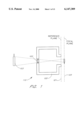
- FIG. 1 shows an imaging system having a reference plane and a focal plane.
- FIG. 2 shows the imaging system of FIG. 1 with an image sensor assembly mounted such that an image sensor is aligned with the focal plane.
- FIG. 3 shows a top view of an image sensor assembly.
- FIG. 4A shows a cross section view of a cut-plane "A" from the image sensor assembly shown in FIG. 3.
- FIG. 4B shows a cross section view of a cut-plane "B" from the image sensor assembly shown in FIG. 3.
- FIG. 5A shows a cross section view of an image sensor assembly wherein the reference members are incorporated into the window standoff frame.
- FIG. 5B shows a cross section view of an image sensor assembly wherein the reference members are incorporated into the window standoff frame, the image sensor die sits in a recessed shoulder in the window standoff frame, and the back plate is bonded to a lower frame.
- FIG. 5C shows a cross section view of an image sensor assembly wherein the reference members are incorporated into the window standoff frame, the image sensor die sits in a recessed shoulder in the window standoff frame, and the back plate is bonded to the window standoff frame.
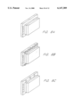
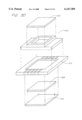
- FIG. 5D shows an exploded view of the image sensor assembly shown in FIGS. 5A-5C.
- FIG. 6A shows reference members where the reference plane is established by one or more upper surfaces.
- FIG. 6B shows reference members where the reference plane is established by pads on an upper surface of the reference members.
- FIG. 6C shows reference members where the reference plane is established by protrusions on an upper surface of the reference members.
- FIG. 7A shows a cross section view of an image sensor assembly wherein the image sensor die is electrically connected to an upper frame.
- FIG. 7B shows an underside (connector side) view of the assembly shown in FIG. 7A.
- FIG. 7C shows an upper side (window side) view of the assembly shown in FIG. 7A.
- FIG. 7D shows an exploded view of the assembly shown in FIGS. 7A-7C.
- FIG. 1 shows an imaging system 110 having a reference plane 101 and a focal plane 105.
- the focal plane corresponds to the focal plane of a lens 102.
- the lens 102 is attached to a housing assembly 100, where a portion of the housing assembly 100 defines the reference plane 101.
- the lens 102 focuses an image of an object 103 onto the focal plane 105.
- the focal plane 105 lies behind the reference plane 101.
- the focal plane 105 lies in front of the reference plane 101.
- the focal plane 105 is coincident with the reference plane 101.
- the imaging system 110 is typical of cameras where the housing assembly 100 corresponds to the camera body and the lens 102 corresponds to the camera lens.
- a typical film camera e.g., a 35 mm camera, a large-format camera, a view camera, etc.
- the film is pressed against the portion of the housing assembly 100 that defines the reference plane 101 and the lens 102 is positioned such that the focal plane 105 and the reference plane 101 coincide.
- FIG. 2 shows the imaging system 110 with an image sensor assembly 210 mounted on the housing assembly 100.
- the image sensor assembly 210 includes a sensor surface 212 and reference members 214.
- the reference members 214 are positioned with respect to the sensor surface 212 such that when the reference members are in contact with the portion of the housing 100 that defines the reference plane 101, the sensor surface 212 is desirably positioned with respect to the focal plane 105.
- the reference members 214 are positioned with respect to the sensor surface 212 such that when the reference members are in contact with the portion of the housing 100 that defines the reference plane 101, the sensor surface 212 is very near the focal plane 105.
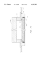
- FIG. 3 shows a top view of an image sensor assembly 300 that can be used as an embodiment of the image sensor assembly 210.
- the image sensor assembly 300 includes a window standoff frame 304 and a housing frame 310.
- the housing frame 310 can be constructed from any insulating material, including plastic, ceramic, glass, etc.
- the housing frame 310 includes one or more conductive members 316.
- the conductive members 316 can be surface mount pads, leads, pints for thru-hole mounting, J-leads, gull-wing leads, Flexsol ribbon connectors, edge metalization, leadless solder connections, ball grid array connectors, wire bond connectors, leadless conductive epoxy pads, z-axis elastomer pads, etc.
- One or more bond wires 314 provide electrical connection between the conductive members 316 and an integrated circuit sensor die 306.
- the bond wires 314 are positioned on left and right sides of the frame 310.
- Reference members 312 are provided on one or more portions of the housing frame 310.
- the reference members 312 may be attached (e.g., bonded) to the housing frame 310 or formed integrally with the frame 310.
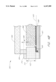
- FIG. 4A shows a cross section view of a cut-plane "A" though a left (or right) side of the image sensor assembly 300 shown in FIG. 3.
- a lower portion of the window standoff frame 304 is bonded to an upper portion of the housing frame 310 and a window 302 is bonded to an upper portion of the window standoff frame 304.
- the window 302 is positioned over the die 306, thereby allowing light to reach an upper surface of the die 306.
- a lower surface of the die 306 is bonded to a plate 308.
- the plate 308 is rigid enough to support the die 306.
- the plate 308 is a metal plate.
- the plate 308 is bonded to a lower portion of the frame 310 by an adhesive 420.
- the adhesive 420 can be an epoxy adhesive, an elastomeric adhesive, a resin adhesive, a cyano-acrylate adhesive, a thermoplastic adhesive, etc.
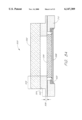
- FIG. 4B shows a cross section view of a cut plane "B" through a top (or bottom) side of the image sensor assembly 300 shown in FIG. 3.
- an upper portion of the reference member 312 defines a reference plane substantially parallel to an image plane of the die 306.
- a dimension T 450, between the reference plane and the upper surface of the die is held to a desired tolerance.
- the term image plane includes a plane in which a focused image is to be formed in order for the focused image to be sensed by the circuits on the image sensor die 306.
- the image plane corresponds to the focal plane of the lens 102.
- the image plane of the image sensor die 306 is typically a known distance from, and coplanar with, the upper surface of the die. For many image sensor dies, the image plane corresponds to the upper surface of the die 306 having light sensing elements thereon.
- the presence of micro-lenses attached to the image sensor die 306 and/or a window or lens can move the image plane away from the upper surface of the die 306.
- the distance between the image plane and the upper surface of the die is typically known, such that by mounting the upper surface of the image sensor die 302 with reference to a reference plane, the image plane is thereby positioned at a predictable distance with respect to the reference plane.
- the tolerance T 450 can be provided by machining the reference member 312 after the plate 308 (carrying the die 306) is bonded to the frame 310.
- the tolerance T 450 can be provided by bonding the plate 308 (carrying the die 306) to the frame 310 using a jig (not shown) such that the sensor surface is held in a desired position relative to the reference plane during the bonding process.
- the spacing T 450 is controlled primarily by thermal expansion of the thickness of the die 306, the plate 308, the bond line between the die 306 and the plate 308, the adhesive 420, a shoulder region 422 of the frame 310, and the reference member 312.
- An optional lower cover 401 can be bonded to a lower surface of the frame 310 to further protect the die 306 and the plate 308.
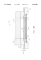
- FIG. 5A shows a cross section view of an image sensor assembly 500 wherein a reference member that establishes a reference plane is incorporated into a window standoff frame 504.
- a first upper portion 506 of the window standoff frame 504 supports the window 302.
- a second upper portion 505 of the window standoff frame 504 establishes the reference plane.
- the window standoff frame 504 is bonded to the frame 310.
- the die 306 is bonded to the plate 308 and the plate is bonded to the frame 310 by an adhesive 420.
- the upper surface of the die 306 (the upper surface having the image sensor) is in close proximity, or actual contact, with a lower surface of the window standoff frame 504.
- a thickness T 508 between the second upper surface 505 and the lower surface of the window standoff frame 504 determines the spacing between the reference plane (established by the second upper surface 505) and the surface of the image sensor die 306.
- the thickness of the image sensor die 306 does not affect the spacing or alignment between the reference plane and the image plane of the sensor.
- the mechanical tolerances of the plate 308, the bond 420, and the lower frame 310 do not affect the spacing or alignment of between the reference plane and the image plane of the sensor.
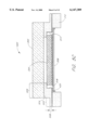
- FIG. 5B shows a cross section view of an image sensor assembly 510 that is similar to the assembly 500, except that the image sensor die 306 rests against a recessed standoff shoulder 518.
- the recessed standoff shoulder 518 is recessed by a recess thickness 511.
- the plate 308 is bonded to the frame 310.
- the distance between the top surface of the image sensor die 306 and the reference plane is determined primarily by the difference between the recess thickness 511 and the thickness T 508.
- the assembly 510 allows the top surface of the image sensor die 306 to be placed in the reference plane or even above the reference plane as desired. By adjusting the dimensions 508 and 511, the image plane can be placed in front of the reference plane, coincident with the reference plane, or behind the reference plane, as desired.
- FIG. 5C shows a cross section view of an image sensor assembly 520 that is similar to the assembly 510, except that the plate 308 is bonded to the window standoff frame 504.
- FIG. 5D shows an exploded view of the assemblies illustrated in FIGS. 5A-5C.
- the thickness T 508 can be reduced to zero in FIGS. 5A-5C such that the reference member is a portion of the upper surface of the frame 310.
- the spacing and alignment between the reference plane and the image plane will be a function of the thickness of the bond line between the window standoff frame 504 and the frame 310.
- the optional second cover 401 can be bonded to a lower surface of the frame 310 shown in FIGS. 5A-5C.
- the image sensor assemblies 500, 510, and 520 are similar to the image sensor assemblies shown in FIGS. 3 and 4.
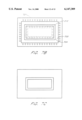
- FIGS. 6A-6C show various embodiments of the reference members described in FIGS. 3-5.
- the reference plane is established by a substantially planar smooth upper surface 602 of the reference member.
- the reference plane is established by a plurality of pads 608 formed on an upper surface of the reference member. Each pad 608 has a surface that is substantially planar. The shape of the pads 608 can be rectangular, circular, triangular, oval, trapezoidal, linear, rail-like, etc.
- the reference plane is established by a plurality of protrusions 628 provided on an upper surface of the reference member.
- the protrusions 628 can be hemispherical, conical, truncated-conical, etc.
- FIG. 7A shows a cross section view of an image sensor assembly 700 wherein the image sensor die is electrically connected to an upper frame.
- FIG. 7B shows an underside view of the assembly 700
- FIG. 7C shows a top side view of the assembly 700
- FIG. 7D shows an exploded view of the assembly 700.
- a first upper portion of a window standoff frame 701 supports the window 302.
- a second upper portion of the window standoff frame 701 establishes the reference plane.
- the window standoff frame 701 is bonded to the frame 310.
- the die 306 is bonded to a plate 308 and the plate is bonded to the frame 310 by an adhesive 420.
- the upper surface of the die 306 When bonded, the upper surface of the die 306 (the upper surface having the image sensor) is in close proximity, or actual contact, with a lower surface of the window standoff frame 701.
- An electrical contact 703 connects an electrical lead (or pad) on the upper surface of the die 306 to an electrical trace 704 on the lower surface of the window frame 701 (as shown in FIG. 5B).
- the trace 704 ends in an electrical pad 705.
- FIGS. 7A and 7B many such connections can be provided between the die 306 and pads on the window frame 701.
- the pads on the window frame can be provided on one, two, three, or four sides of the window frame 701.
- FIG. 7B shows electrical pads on all four sides of the window frame 701.
- the pads, such as the pad 705, can be electrically connected to a circuit board or flexible circuit 710 as shown.
- the electrical contact 703 can be, for example, a flip chip connection, a Tape-Automated Bond (TAD), and the like.
- flip chip connections include solder connections, conductive adhesives, gold pads, conductive polymer bumps, etc.
Abstract
Description
Claims (15)
Priority Applications (3)
| Application Number | Priority Date | Filing Date | Title |
|---|---|---|---|
| US09/362,507 US6147389A (en) | 1999-06-04 | 1999-07-27 | Image sensor package with image plane reference |
| AU51813/00A AU5181300A (en) | 1999-06-04 | 2000-06-02 | Image sensor package with image plane reference |
| PCT/US2000/040062 WO2000076001A1 (en) | 1999-06-04 | 2000-06-02 | Image sensor package with image plane reference |
Applications Claiming Priority (2)
| Application Number | Priority Date | Filing Date | Title |
|---|---|---|---|
| US13776299P | 1999-06-04 | 1999-06-04 | |
| US09/362,507 US6147389A (en) | 1999-06-04 | 1999-07-27 | Image sensor package with image plane reference |
Publications (1)
| Publication Number | Publication Date |
|---|---|
| US6147389A true US6147389A (en) | 2000-11-14 |
Family
ID=26835557
Family Applications (1)
| Application Number | Title | Priority Date | Filing Date |
|---|---|---|---|
| US09/362,507 Expired - Fee Related US6147389A (en) | 1999-06-04 | 1999-07-27 | Image sensor package with image plane reference |
Country Status (3)
| Country | Link |
|---|---|
| US (1) | US6147389A (en) |
| AU (1) | AU5181300A (en) |
| WO (1) | WO2000076001A1 (en) |
Cited By (55)
| Publication number | Priority date | Publication date | Assignee | Title |
|---|---|---|---|---|
| US6396116B1 (en) * | 2000-02-25 | 2002-05-28 | Agilent Technologies, Inc. | Integrated circuit packaging for optical sensor devices |
| EP1237202A2 (en) * | 2001-02-28 | 2002-09-04 | Fujitsu Limited | Semiconductor device and method for making the same |
| US6509560B1 (en) | 2000-11-13 | 2003-01-21 | Amkor Technology, Inc. | Chip size image sensor in wirebond package with step-up ring for electrical contact |
| KR100370117B1 (en) * | 2001-01-15 | 2003-01-30 | 앰코 테크놀로지 코리아 주식회사 | semiconductor package and manufacturing method the same |
| US6528857B1 (en) * | 2000-11-13 | 2003-03-04 | Amkor Technology, Inc. | Chip size image sensor bumped package |
| US20030066591A1 (en) * | 2001-10-09 | 2003-04-10 | Mitsubishi Denki Kabushiki Kaisha | Production method for solid image pickup device |
| US6586824B1 (en) * | 2001-07-26 | 2003-07-01 | Amkor Technology, Inc. | Reduced thickness packaged electronic device |
| US6620646B1 (en) | 2000-11-13 | 2003-09-16 | Amkor Technology, Inc. | Chip size image sensor wirebond package fabrication method |
| US6621616B1 (en) * | 1998-08-21 | 2003-09-16 | Gentex Corporation | Devices incorporating electrochromic elements and optical sensors |
| US6629633B1 (en) | 2000-11-13 | 2003-10-07 | Amkor Technology, Inc. | Chip size image sensor bumped package fabrication method |
| US6635958B2 (en) * | 2001-12-03 | 2003-10-21 | Dover Capital Formation Group | Surface mount ceramic package |
| US6661084B1 (en) * | 2000-05-16 | 2003-12-09 | Sandia Corporation | Single level microelectronic device package with an integral window |
| US20030232461A1 (en) * | 2002-06-04 | 2003-12-18 | Bolken Todd O. | Methods for packaging image sensitive electronic devices |
| US20040036135A1 (en) * | 2002-08-23 | 2004-02-26 | Amkor Technology, Inc. | Optic semiconductor module and manufacturing method |
| US6713876B1 (en) * | 1999-11-04 | 2004-03-30 | Stmicroelectronics S.A. | Optical semiconductor housing and method for making same |
| US20040084741A1 (en) * | 2002-08-28 | 2004-05-06 | Boon Suan Jeung | Leadless packaging for image sensor devices and methods of assembly |
| US20040085476A1 (en) * | 2002-07-11 | 2004-05-06 | Whalen Matthew Stephen | Electronic image capture system with modular components |
| US6734419B1 (en) | 2001-06-28 | 2004-05-11 | Amkor Technology, Inc. | Method for forming an image sensor package with vision die in lens housing |
| EP1432240A1 (en) * | 2002-12-19 | 2004-06-23 | Eastman Kodak Company | Image sensor positioning system and method |
| US20040149908A1 (en) * | 2003-01-31 | 2004-08-05 | Delphi Technologies, Inc. | Deep cavity sensor package |
| US6784534B1 (en) * | 2002-02-06 | 2004-08-31 | Amkor Technology, Inc. | Thin integrated circuit package having an optically transparent window |
| EP1473775A2 (en) * | 2003-04-28 | 2004-11-03 | Matsushita Electric Industrial Co., Ltd. | Method for producing solid-state imaging device |
| US20050057883A1 (en) * | 2003-09-16 | 2005-03-17 | Bolken Todd O. | Moisture-resistant electronic device package and methods of assembly |
| US20050087756A1 (en) * | 2003-10-22 | 2005-04-28 | Akinori Shiraishi | Light transmissive cover, device provided with same and methods for manufacturing them |
| US20050219398A1 (en) * | 2004-03-30 | 2005-10-06 | Fuji Photo Film Co., Ltd. | Image capture apparatus |
| US20050236685A1 (en) * | 2004-04-26 | 2005-10-27 | Matsushita Electric Industrial Co., Ltd. | Optical device and method for fabricating the same |
| US20050242274A1 (en) * | 1999-12-08 | 2005-11-03 | Steven Webster | Camera module |
| US20050247990A1 (en) * | 2004-05-05 | 2005-11-10 | Ming-Te Cheng | Image sensor packages and method of assembling the same |
| US20050253211A1 (en) * | 2004-05-14 | 2005-11-17 | Matsushita Electric Industrial Co., Ltd. | Optical device and method for fabricating the same |
| US20060043461A1 (en) * | 2002-11-20 | 2006-03-02 | Stmicroelectronics S.R.L. | Process for manufacturing a byte selection transistor for a matrix of non volatile memory cells and corresponding structure |
| US7059040B1 (en) | 2001-01-16 | 2006-06-13 | Amkor Technology, Inc. | Optical module with lens integral holder fabrication method |
| US20060261458A1 (en) * | 2003-11-12 | 2006-11-23 | Amkor Technology, Inc. | Semiconductor package and manufacturing method thereof |
| US20060266938A1 (en) * | 2005-05-05 | 2006-11-30 | Stats Chippac Ltd. | Optical Die-Down Quad Flat Non-Leaded Package |
| US20060290801A1 (en) * | 2005-06-24 | 2006-12-28 | Altus Technology Inc. | Digital camera module with improved image quality |
| US7227236B1 (en) | 2005-04-26 | 2007-06-05 | Amkor Technology, Inc. | Image sensor package and its manufacturing method |
| US20070210246A1 (en) * | 2005-04-14 | 2007-09-13 | Amkor Technology, Inc. | Stacked image sensor optical module and fabrication method |
| US20070272827A1 (en) * | 2005-04-27 | 2007-11-29 | Amkor Technology, Inc. | Image sensor package having mount holder attached to image sensor die |
| US7359579B1 (en) | 2004-10-08 | 2008-04-15 | Amkor Technology, Inc. | Image sensor package and its manufacturing method |
| US7375757B1 (en) * | 1999-09-03 | 2008-05-20 | Sony Corporation | Imaging element, imaging device, camera module and camera system |
| US7425750B2 (en) | 1999-12-08 | 2008-09-16 | Amkor Technology, Inc. | Snap lid camera module |
| US20080237824A1 (en) * | 2006-02-17 | 2008-10-02 | Amkor Technology, Inc. | Stacked electronic component package having single-sided film spacer |
| US20090033789A1 (en) * | 2007-08-03 | 2009-02-05 | Hon Hai Precision Industry Co., Ltd. | Camera module |
| US20090096047A1 (en) * | 2007-10-11 | 2009-04-16 | Hon Hai Precision Industry Co., Ltd. | Imaging module package |
| US7576401B1 (en) | 2005-07-07 | 2009-08-18 | Amkor Technology, Inc. | Direct glass attached on die optical module |
| US20090224386A1 (en) * | 2008-03-07 | 2009-09-10 | Stats Chippac, Ltd. | Optical Semiconductor Device Having Pre-Molded Leadframe with Window and Method Therefor |
| US7633144B1 (en) | 2006-05-24 | 2009-12-15 | Amkor Technology, Inc. | Semiconductor package |
| US7675180B1 (en) | 2006-02-17 | 2010-03-09 | Amkor Technology, Inc. | Stacked electronic component package having film-on-wire spacer |
| US7863723B2 (en) | 2001-03-09 | 2011-01-04 | Amkor Technology, Inc. | Adhesive on wire stacked semiconductor package |
| US20110175182A1 (en) * | 2010-01-15 | 2011-07-21 | Yu-Hsiang Chen | Optical Seneor Package Structure And Manufactueing Method Thereof |
| US20130286281A1 (en) * | 2012-04-27 | 2013-10-31 | Canon Kabushiki Kaisha | Image pickup apparatus having image pickup device |
| US20140139710A1 (en) * | 2012-11-19 | 2014-05-22 | Hon Hai Precision Industry Co., Ltd. | Image sensor module and camera module using same |
| DE102013102819A1 (en) * | 2013-03-19 | 2014-09-25 | Conti Temic Microelectronic Gmbh | Camera module and method of manufacture |
| US20140331462A1 (en) * | 2011-10-11 | 2014-11-13 | Taiwan Semiconductor Manufacturing Company, Ltd. | Packaging Process Tools and Packaging Methods for Semiconductor Devices |
| US20150137294A1 (en) * | 2013-11-19 | 2015-05-21 | China Wafer Level Csp Co., Ltd. | Image sensor package structure and method |
| US11094722B2 (en) * | 2016-02-01 | 2021-08-17 | Sony Corporation | Image sensor package and imaging apparatus |
Families Citing this family (1)
| Publication number | Priority date | Publication date | Assignee | Title |
|---|---|---|---|---|
| US7795573B2 (en) | 2008-11-17 | 2010-09-14 | Teledyne Scientific & Imaging, Llc | Detector with mounting hub to isolate temperature induced strain and method of fabricating the same |
Citations (4)
| Publication number | Priority date | Publication date | Assignee | Title |
|---|---|---|---|---|
| US4926227A (en) * | 1986-08-01 | 1990-05-15 | Nanometrics Inc. | Sensor devices with internal packaged coolers |
| US5122561A (en) * | 1989-12-21 | 1992-06-16 | Kuraray Co., Ltd. | Disposable moldings and polymer compositions for their production |
| US5359208A (en) * | 1993-02-26 | 1994-10-25 | Nippon Sheet Glass Co., Ltd. | Chip package with microlens array |
| US5867368A (en) * | 1997-09-09 | 1999-02-02 | Amkor Technology, Inc. | Mounting for a semiconductor integrated circuit device |
Family Cites Families (4)
| Publication number | Priority date | Publication date | Assignee | Title |
|---|---|---|---|---|
| JPH0230181A (en) * | 1988-07-19 | 1990-01-31 | Fujitsu Ltd | Semiconductor device |
| CA2092165C (en) * | 1992-03-23 | 2001-05-15 | Tuyosi Nagano | Chip carrier for optical device |
| JP3161142B2 (en) * | 1993-03-26 | 2001-04-25 | ソニー株式会社 | Semiconductor device |
| KR100186329B1 (en) * | 1996-06-14 | 1999-03-20 | 문정환 | Semiconductor package for charge coupled device |
-
1999
- 1999-07-27 US US09/362,507 patent/US6147389A/en not_active Expired - Fee Related
-
2000
- 2000-06-02 AU AU51813/00A patent/AU5181300A/en not_active Abandoned
- 2000-06-02 WO PCT/US2000/040062 patent/WO2000076001A1/en active Application Filing
Patent Citations (4)
| Publication number | Priority date | Publication date | Assignee | Title |
|---|---|---|---|---|
| US4926227A (en) * | 1986-08-01 | 1990-05-15 | Nanometrics Inc. | Sensor devices with internal packaged coolers |
| US5122561A (en) * | 1989-12-21 | 1992-06-16 | Kuraray Co., Ltd. | Disposable moldings and polymer compositions for their production |
| US5359208A (en) * | 1993-02-26 | 1994-10-25 | Nippon Sheet Glass Co., Ltd. | Chip package with microlens array |
| US5867368A (en) * | 1997-09-09 | 1999-02-02 | Amkor Technology, Inc. | Mounting for a semiconductor integrated circuit device |
Cited By (115)
| Publication number | Priority date | Publication date | Assignee | Title |
|---|---|---|---|---|
| US6621616B1 (en) * | 1998-08-21 | 2003-09-16 | Gentex Corporation | Devices incorporating electrochromic elements and optical sensors |
| US7375757B1 (en) * | 1999-09-03 | 2008-05-20 | Sony Corporation | Imaging element, imaging device, camera module and camera system |
| US6713876B1 (en) * | 1999-11-04 | 2004-03-30 | Stmicroelectronics S.A. | Optical semiconductor housing and method for making same |
| US20070012864A1 (en) * | 1999-12-08 | 2007-01-18 | Amkor Technology, Inc. | Camera module fabrication method |
| US20080308717A1 (en) * | 1999-12-08 | 2008-12-18 | Amkor Technology, Inc. | Camera module with window mechanical attachment |
| US7332712B2 (en) | 1999-12-08 | 2008-02-19 | Amkor Technology, Inc. | Camera module fabrication method including the step of removing a lens mount and window from the mold |
| US9735191B2 (en) | 1999-12-08 | 2017-08-15 | Amkor Technology, Inc. | Molded semiconductor package |
| US8994860B2 (en) | 1999-12-08 | 2015-03-31 | Amkor, Technology, Inc. | Molded image sensor package and method |
| US20050242274A1 (en) * | 1999-12-08 | 2005-11-03 | Steven Webster | Camera module |
| US7199359B2 (en) | 1999-12-08 | 2007-04-03 | Amkor Technology, Inc. | Camera module fabrication method including singulating a substrate |
| US9332164B2 (en) | 1999-12-08 | 2016-05-03 | Amkor Technology, Inc. | Molded semiconductor package with snap lid |
| US7425750B2 (en) | 1999-12-08 | 2008-09-16 | Amkor Technology, Inc. | Snap lid camera module |
| US7786429B2 (en) | 1999-12-08 | 2010-08-31 | Amkor Technology, Inc. | Camera module with window mechanical attachment |
| US7126111B2 (en) | 1999-12-08 | 2006-10-24 | Amkor Technology, Inc. | Camera module having a threaded lens barrel and a ball grid array connecting device |
| US6396116B1 (en) * | 2000-02-25 | 2002-05-28 | Agilent Technologies, Inc. | Integrated circuit packaging for optical sensor devices |
| US6661084B1 (en) * | 2000-05-16 | 2003-12-09 | Sandia Corporation | Single level microelectronic device package with an integral window |
| US6629633B1 (en) | 2000-11-13 | 2003-10-07 | Amkor Technology, Inc. | Chip size image sensor bumped package fabrication method |
| US6528857B1 (en) * | 2000-11-13 | 2003-03-04 | Amkor Technology, Inc. | Chip size image sensor bumped package |
| US6509560B1 (en) | 2000-11-13 | 2003-01-21 | Amkor Technology, Inc. | Chip size image sensor in wirebond package with step-up ring for electrical contact |
| US6620646B1 (en) | 2000-11-13 | 2003-09-16 | Amkor Technology, Inc. | Chip size image sensor wirebond package fabrication method |
| KR100370117B1 (en) * | 2001-01-15 | 2003-01-30 | 앰코 테크놀로지 코리아 주식회사 | semiconductor package and manufacturing method the same |
| US7059040B1 (en) | 2001-01-16 | 2006-06-13 | Amkor Technology, Inc. | Optical module with lens integral holder fabrication method |
| US7609461B1 (en) | 2001-01-16 | 2009-10-27 | Amkor Technology, Inc. | Optical module having cavity substrate |
| EP1237202A2 (en) * | 2001-02-28 | 2002-09-04 | Fujitsu Limited | Semiconductor device and method for making the same |
| EP1237202A3 (en) * | 2001-02-28 | 2004-12-08 | Fujitsu Limited | Semiconductor device and method for making the same |
| US8143727B2 (en) | 2001-03-09 | 2012-03-27 | Amkor Technology, Inc. | Adhesive on wire stacked semiconductor package |
| US7863723B2 (en) | 2001-03-09 | 2011-01-04 | Amkor Technology, Inc. | Adhesive on wire stacked semiconductor package |
| US6734419B1 (en) | 2001-06-28 | 2004-05-11 | Amkor Technology, Inc. | Method for forming an image sensor package with vision die in lens housing |
| US6586824B1 (en) * | 2001-07-26 | 2003-07-01 | Amkor Technology, Inc. | Reduced thickness packaged electronic device |
| US20030066591A1 (en) * | 2001-10-09 | 2003-04-10 | Mitsubishi Denki Kabushiki Kaisha | Production method for solid image pickup device |
| US6805767B2 (en) * | 2001-10-09 | 2004-10-19 | Renesas Technology Corp. | Method for producing solid-state image pickup device |
| US6635958B2 (en) * | 2001-12-03 | 2003-10-21 | Dover Capital Formation Group | Surface mount ceramic package |
| US6784534B1 (en) * | 2002-02-06 | 2004-08-31 | Amkor Technology, Inc. | Thin integrated circuit package having an optically transparent window |
| US20060051892A1 (en) * | 2002-06-04 | 2006-03-09 | Bolken Todd O | Methods for packaging image sensitive electronic devices |
| US6906403B2 (en) * | 2002-06-04 | 2005-06-14 | Micron Technology, Inc. | Sealed electronic device packages with transparent coverings |
| US20050116355A1 (en) * | 2002-06-04 | 2005-06-02 | Bolken Todd O. | Packages for image sensitive electronic devices |
| US20030232461A1 (en) * | 2002-06-04 | 2003-12-18 | Bolken Todd O. | Methods for packaging image sensitive electronic devices |
| US20060046351A1 (en) * | 2002-06-04 | 2006-03-02 | Bolken Todd O | Methods for packaging image sensitive electronic devices |
| US7195940B2 (en) | 2002-06-04 | 2007-03-27 | Micron Technology, Inc. | Methods for packaging image sensitive electronic devices |
| US20060051891A1 (en) * | 2002-06-04 | 2006-03-09 | Bolken Todd O | Methods for packaging image sensitive electronic devices |
| US7387902B2 (en) | 2002-06-04 | 2008-06-17 | Micron Technology, Inc. | Methods for packaging image sensitive electronic devices |
| US7553688B2 (en) | 2002-06-04 | 2009-06-30 | Micron Technology, Inc. | Methods for packaging image sensitive electronic devices |
| US20060267169A1 (en) * | 2002-06-04 | 2006-11-30 | Bolken Todd O | Image sensitive electronic device packages |
| US7419854B2 (en) | 2002-06-04 | 2008-09-02 | Micron Technology, Inc. | Methods for packaging image sensitive electronic devices |
| US20040085476A1 (en) * | 2002-07-11 | 2004-05-06 | Whalen Matthew Stephen | Electronic image capture system with modular components |
| US20040036135A1 (en) * | 2002-08-23 | 2004-02-26 | Amkor Technology, Inc. | Optic semiconductor module and manufacturing method |
| US7146106B2 (en) | 2002-08-23 | 2006-12-05 | Amkor Technology, Inc. | Optic semiconductor module and manufacturing method |
| US7112471B2 (en) | 2002-08-28 | 2006-09-26 | Micron Technology, Inc. | Leadless packaging for image sensor devices and methods of assembly |
| US20040084741A1 (en) * | 2002-08-28 | 2004-05-06 | Boon Suan Jeung | Leadless packaging for image sensor devices and methods of assembly |
| US7274094B2 (en) | 2002-08-28 | 2007-09-25 | Micron Technology, Inc. | Leadless packaging for image sensor devices |
| US20060043461A1 (en) * | 2002-11-20 | 2006-03-02 | Stmicroelectronics S.R.L. | Process for manufacturing a byte selection transistor for a matrix of non volatile memory cells and corresponding structure |
| EP1432240A1 (en) * | 2002-12-19 | 2004-06-23 | Eastman Kodak Company | Image sensor positioning system and method |
| US20040149908A1 (en) * | 2003-01-31 | 2004-08-05 | Delphi Technologies, Inc. | Deep cavity sensor package |
| US7022990B2 (en) * | 2003-01-31 | 2006-04-04 | Delphi Technologies, Inc. | Deep cavity sensor package |
| EP1473775A3 (en) * | 2003-04-28 | 2006-01-11 | Matsushita Electric Industrial Co., Ltd. | Method for producing solid-state imaging device |
| EP1473775A2 (en) * | 2003-04-28 | 2004-11-03 | Matsushita Electric Industrial Co., Ltd. | Method for producing solid-state imaging device |
| US20100264532A1 (en) * | 2003-09-16 | 2010-10-21 | Micron Technology, Inc. | Electronic device package |
| US20050057883A1 (en) * | 2003-09-16 | 2005-03-17 | Bolken Todd O. | Moisture-resistant electronic device package and methods of assembly |
| US7026548B2 (en) | 2003-09-16 | 2006-04-11 | Micron Technology, Inc. | Moisture-resistant electronic device package and methods of assembly |
| US8508034B2 (en) | 2003-09-16 | 2013-08-13 | Micron Technology, Inc. | Electronic devices |
| US6953891B2 (en) | 2003-09-16 | 2005-10-11 | Micron Technology, Inc. | Moisture-resistant electronic device package and methods of assembly |
| US8115296B2 (en) | 2003-09-16 | 2012-02-14 | Micron Technology, Inc. | Electronic device package |
| US20050263312A1 (en) * | 2003-09-16 | 2005-12-01 | Bolken Todd O | Moisture-resistant electronic device package and methods of assembly |
| US20060169490A1 (en) * | 2003-09-16 | 2006-08-03 | Bolken Todd O | Molding tool and a method of forming an electronic device package |
| US7274096B2 (en) * | 2003-10-22 | 2007-09-25 | Shinko Electric Industries, Co., Ltd. | Light transmissive cover, device provided with same and methods for manufacturing them |
| US20050087756A1 (en) * | 2003-10-22 | 2005-04-28 | Akinori Shiraishi | Light transmissive cover, device provided with same and methods for manufacturing them |
| US8017443B2 (en) | 2003-10-22 | 2011-09-13 | Shinko Electric Industries Co., Ltd | Light transmissive cover, device provided with same and methods for manufacturing them |
| US20060261458A1 (en) * | 2003-11-12 | 2006-11-23 | Amkor Technology, Inc. | Semiconductor package and manufacturing method thereof |
| US20050219398A1 (en) * | 2004-03-30 | 2005-10-06 | Fuji Photo Film Co., Ltd. | Image capture apparatus |
| US7515203B2 (en) * | 2004-03-30 | 2009-04-07 | Fujifilm Corporation | Image capture apparatus |
| US20050236685A1 (en) * | 2004-04-26 | 2005-10-27 | Matsushita Electric Industrial Co., Ltd. | Optical device and method for fabricating the same |
| US7511367B2 (en) | 2004-04-26 | 2009-03-31 | Panasonic Corporation | Optical device and method for fabricating the same |
| US20050247990A1 (en) * | 2004-05-05 | 2005-11-10 | Ming-Te Cheng | Image sensor packages and method of assembling the same |
| US7563644B2 (en) | 2004-05-14 | 2009-07-21 | Panasonic Corporation | Optical device and method for fabricating the same |
| US7436053B2 (en) * | 2004-05-14 | 2008-10-14 | Matsushita Electric Industrial Co., Ltd. | Optical device and method for fabricating the same |
| US20050253211A1 (en) * | 2004-05-14 | 2005-11-17 | Matsushita Electric Industrial Co., Ltd. | Optical device and method for fabricating the same |
| US7359579B1 (en) | 2004-10-08 | 2008-04-15 | Amkor Technology, Inc. | Image sensor package and its manufacturing method |
| US20070210246A1 (en) * | 2005-04-14 | 2007-09-13 | Amkor Technology, Inc. | Stacked image sensor optical module and fabrication method |
| US7227236B1 (en) | 2005-04-26 | 2007-06-05 | Amkor Technology, Inc. | Image sensor package and its manufacturing method |
| US20070272827A1 (en) * | 2005-04-27 | 2007-11-29 | Amkor Technology, Inc. | Image sensor package having mount holder attached to image sensor die |
| US7736930B2 (en) | 2005-05-05 | 2010-06-15 | Stats Chippac, Ltd. | Optical die-down quad flat non-leaded package |
| US7495325B2 (en) * | 2005-05-05 | 2009-02-24 | Stats Chippac, Ltd. | Optical die-down quad flat non-leaded package |
| US20090162965A1 (en) * | 2005-05-05 | 2009-06-25 | Stats Chippac, Ltd. | Optical Die-Down Quad Flat Non-Leaded Package |
| US20060266938A1 (en) * | 2005-05-05 | 2006-11-30 | Stats Chippac Ltd. | Optical Die-Down Quad Flat Non-Leaded Package |
| US20060290801A1 (en) * | 2005-06-24 | 2006-12-28 | Altus Technology Inc. | Digital camera module with improved image quality |
| US7576401B1 (en) | 2005-07-07 | 2009-08-18 | Amkor Technology, Inc. | Direct glass attached on die optical module |
| US7911017B1 (en) | 2005-07-07 | 2011-03-22 | Amkor Technology, Inc. | Direct glass attached on die optical module |
| US20080237824A1 (en) * | 2006-02-17 | 2008-10-02 | Amkor Technology, Inc. | Stacked electronic component package having single-sided film spacer |
| US7675180B1 (en) | 2006-02-17 | 2010-03-09 | Amkor Technology, Inc. | Stacked electronic component package having film-on-wire spacer |
| US8072083B1 (en) | 2006-02-17 | 2011-12-06 | Amkor Technology, Inc. | Stacked electronic component package having film-on-wire spacer |
| US8129849B1 (en) | 2006-05-24 | 2012-03-06 | Amkor Technology, Inc. | Method of making semiconductor package with adhering portion |
| US7633144B1 (en) | 2006-05-24 | 2009-12-15 | Amkor Technology, Inc. | Semiconductor package |
| US20090033789A1 (en) * | 2007-08-03 | 2009-02-05 | Hon Hai Precision Industry Co., Ltd. | Camera module |
| CN101359081B (en) * | 2007-08-03 | 2010-09-29 | 鸿富锦精密工业(深圳)有限公司 | Camera module |
| US7782390B2 (en) | 2007-08-03 | 2010-08-24 | Hon Hai Precision Industry Co., Ltd. | Camera module |
| US7928526B2 (en) * | 2007-10-11 | 2011-04-19 | Hon Hai Precision Industry Co., Ltd. | Imaging module package |
| US20090096047A1 (en) * | 2007-10-11 | 2009-04-16 | Hon Hai Precision Industry Co., Ltd. | Imaging module package |
| US20120168806A1 (en) * | 2008-03-07 | 2012-07-05 | Stats Chippac, Ltd. | Optical Semiconductor Device having Pre-Molded Leadframe with Window and Method Therefor |
| US8138027B2 (en) * | 2008-03-07 | 2012-03-20 | Stats Chippac, Ltd. | Optical semiconductor device having pre-molded leadframe with window and method therefor |
| US8586422B2 (en) * | 2008-03-07 | 2013-11-19 | Stats Chippac, Ltd. | Optical semiconductor device having pre-molded leadframe with window and method therefor |
| US9397236B2 (en) | 2008-03-07 | 2016-07-19 | STATS ChipPAC Pte. Ltd. | Optical semiconductor device having pre-molded leadframe with window and method therefor |
| US20090224386A1 (en) * | 2008-03-07 | 2009-09-10 | Stats Chippac, Ltd. | Optical Semiconductor Device Having Pre-Molded Leadframe with Window and Method Therefor |
| US8169043B2 (en) * | 2010-01-15 | 2012-05-01 | Cheng Uei Precision Industry Co., Ltd. | Optical seneor package structure and manufactueing method thereof |
| US20110175182A1 (en) * | 2010-01-15 | 2011-07-21 | Yu-Hsiang Chen | Optical Seneor Package Structure And Manufactueing Method Thereof |
| US20140331462A1 (en) * | 2011-10-11 | 2014-11-13 | Taiwan Semiconductor Manufacturing Company, Ltd. | Packaging Process Tools and Packaging Methods for Semiconductor Devices |
| US9218999B2 (en) * | 2011-10-11 | 2015-12-22 | Taiwan Semiconductor Manufacturing Company, Ltd. | Packaging process tools and packaging methods for semiconductor devices |
| US9065989B2 (en) * | 2012-04-27 | 2015-06-23 | Canon Kabushiki Kaisha | Image pickup apparatus having image pickup device |
| US20130286281A1 (en) * | 2012-04-27 | 2013-10-31 | Canon Kabushiki Kaisha | Image pickup apparatus having image pickup device |
| US9041849B2 (en) * | 2012-11-19 | 2015-05-26 | Hon Hai Precision Industry Co., Ltd. | Image sensor module and camera module using same |
| US20140139710A1 (en) * | 2012-11-19 | 2014-05-22 | Hon Hai Precision Industry Co., Ltd. | Image sensor module and camera module using same |
| DE102013102819A1 (en) * | 2013-03-19 | 2014-09-25 | Conti Temic Microelectronic Gmbh | Camera module and method of manufacture |
| US9485400B2 (en) | 2013-03-19 | 2016-11-01 | Conti Temic Microelectronic Gmbh | Camera module and method for the production thereof |
| US20150137294A1 (en) * | 2013-11-19 | 2015-05-21 | China Wafer Level Csp Co., Ltd. | Image sensor package structure and method |
| US9299735B2 (en) * | 2013-11-19 | 2016-03-29 | China Wafer Level Csp Co., Ltd. | Image sensor package structure and method |
| US11094722B2 (en) * | 2016-02-01 | 2021-08-17 | Sony Corporation | Image sensor package and imaging apparatus |
Also Published As
| Publication number | Publication date |
|---|---|
| AU5181300A (en) | 2000-12-28 |
| WO2000076001A1 (en) | 2000-12-14 |
Similar Documents
| Publication | Publication Date | Title |
|---|---|---|
| US6147389A (en) | Image sensor package with image plane reference | |
| CN105847645B (en) | Camera module based on integrated packaging process, integrated base assembly and manufacturing method thereof | |
| US6268231B1 (en) | Low cost CCD packaging | |
| TWI437301B (en) | Camera module | |
| US7250663B2 (en) | Frame scale package using contact lines through the elements | |
| US8714843B2 (en) | Camera module and method of manufacturing the same | |
| CN107566691B (en) | Photosensitive assembly, camera module and manufacturing method thereof | |
| KR20180132684A (en) | Camera module, its photosensitive part and method of manufacturing the same | |
| US7153042B2 (en) | Optic device | |
| US5418566A (en) | Compact imaging apparatus for electronic endoscope with improved optical characteristics | |
| US6798053B2 (en) | IC chip package | |
| WO1997005660A1 (en) | Solid-state image pickup device and its manufacture | |
| JPH0936339A (en) | Image sensor assembly and its packaging method | |
| KR20080070067A (en) | Semiconductor package, method of producing the same, semiconductor module, and electronic apparatus | |
| US20040256687A1 (en) | Optical module, method of manufacturing the same, and electronic instrument | |
| WO2022033294A1 (en) | Anti-shake photographing module and preparation method therefor | |
| US6967400B2 (en) | IC chip package | |
| US20140113399A1 (en) | Manufacturing method of solid-state imaging apparatus, solid-state imaging apparatus, and electronic imaging apparatus | |
| JPH11252416A (en) | Attaching method for solid-state image-pickup device | |
| US5801374A (en) | Precision optical sensor packaging | |
| JP3495008B2 (en) | Solid-state imaging device and manufacturing method thereof | |
| CN217087989U (en) | Photoelectric module and electronic equipment | |
| CN213718044U (en) | Camera module and electronic equipment | |
| JP3567740B2 (en) | Semiconductor sensor and mounting structure | |
| JPH0813107B2 (en) | Solid-state imaging device |
Legal Events
| Date | Code | Title | Description |
|---|---|---|---|
| AS | Assignment |
Owner name: SILICON FILM TECHNOLOGIES, INC., CALIFORNIA Free format text: ASSIGNMENT OF ASSIGNORS INTEREST;ASSIGNORS:MICHAEL, JONATHAN;SAPIR, STERN ITZHAK;HORNBACK, WILLIAM B.;REEL/FRAME:010138/0782;SIGNING DATES FROM 19990722 TO 19990726 |
|
| AS | Assignment |
Owner name: SILICON FILM TECHNOLOGIES, INC., CALIFORNIA Free format text: CORRECTION OF NAMES OF CONVEYING PARTIES TO 1) JONATHAN MICHAEL STERN, 2) ITZHAK SAPIR, 3) WILLIAM E. HORNBACK, PREVIOUSLY RECORDED AT REEL 010138, FRAME 0782.;ASSIGNORS:STERN, JONATHAN MICHAEL;SAPIR, ITZHAK;HORNBACK, WILLIAM B.;REEL/FRAME:010430/0772;SIGNING DATES FROM 19990722 TO 19990726 |
|
| AS | Assignment |
Owner name: KNOBBE MARTENS OLSON & BEAR, LLP, CALIFORNIA Free format text: SECURITY INTEREST;ASSIGNOR:SILICON FILM TECHNOLOGIES;REEL/FRAME:011796/0374 Effective date: 20010416 |
|
| FPAY | Fee payment |
Year of fee payment: 4 |
|
| FPAY | Fee payment |
Year of fee payment: 8 |
|
| REMI | Maintenance fee reminder mailed | ||
| LAPS | Lapse for failure to pay maintenance fees | ||
| STCH | Information on status: patent discontinuation |
Free format text: PATENT EXPIRED DUE TO NONPAYMENT OF MAINTENANCE FEES UNDER 37 CFR 1.362 |
|
| FP | Lapsed due to failure to pay maintenance fee |
Effective date: 20121114 |