US6147522A - Reference voltage circuitry for use in switched-capacitor applications - Google Patents
Reference voltage circuitry for use in switched-capacitor applications Download PDFInfo
- Publication number
- US6147522A US6147522A US09/224,390 US22439098A US6147522A US 6147522 A US6147522 A US 6147522A US 22439098 A US22439098 A US 22439098A US 6147522 A US6147522 A US 6147522A
- Authority
- US
- United States
- Prior art keywords
- capacitor
- circuitry
- voltage
- sampling
- analog
- Prior art date
- Legal status (The legal status is an assumption and is not a legal conclusion. Google has not performed a legal analysis and makes no representation as to the accuracy of the status listed.)
- Expired - Lifetime
Links
Images
Classifications
-
- H—ELECTRICITY
- H03—ELECTRONIC CIRCUITRY
- H03M—CODING; DECODING; CODE CONVERSION IN GENERAL
- H03M3/00—Conversion of analogue values to or from differential modulation
- H03M3/30—Delta-sigma modulation
- H03M3/322—Continuously compensating for, or preventing, undesired influence of physical parameters
- H03M3/368—Continuously compensating for, or preventing, undesired influence of physical parameters of noise other than the quantisation noise already being shaped inherently by delta-sigma modulators
-
- H—ELECTRICITY
- H03—ELECTRONIC CIRCUITRY
- H03M—CODING; DECODING; CODE CONVERSION IN GENERAL
- H03M3/00—Conversion of analogue values to or from differential modulation
- H03M3/30—Delta-sigma modulation
- H03M3/50—Digital/analogue converters using delta-sigma modulation as an intermediate step
- H03M3/502—Details of the final digital/analogue conversion following the digital delta-sigma modulation
Definitions
- the present invention relates in general to electronic circuits and in particular to reference voltage circuitry for use in switched-capacitor application and systems and methods using the same.
- Audio is important in many multimedia applications, such as gaming and telecommunications. Audio functionality is therefore typically available on most conventional PCS, either in the form of an add-on audio board or as a standard feature provided on the motherboard itself. In fact, PC users increasingly expect not only audio functionality but high quality sound capability.
- the Codec converts input analog audio information into a digital format for processing by a companion digital audio processor.
- the digital processor for example may support sample rate conversion, SoundBlaster compatibility, wavetable synthesis, or DirectSound acceleration, among other things.
- the Codec also converts outgoing signals from the audio processor from digital-to-analog format for eventual audible output to the user.
- the Codec may also mix analog and/or digital audio streams.
- DACs digital to analog converters
- ADCs analog to digital converters
- a reference voltage source must be provided whether it be external and coupled to the chip through a dedicated pin or on-chip, such as with a band gap reference.
- the reference source must meet certain minimum criteria. Among other things, it must be small, low power consuming and have a good power supply rejection ratio (PSRR).
- PSRR power supply rejection ratio
- different DACs and ADCs often require the generation of different reference voltages. Therefore, the need has arisen for circuits and methods for generating reference voltages which not only meet the above performance criteria, but also allows for the scaling of the reference voltage with the DC value of the power supply voltage.
- the principles of the present invention are embodied in circuitry for sampling a reference voltage with a capacitor and includes a first switch for selectively coupling the capacitor to a source of a first reference signal during a first operating phase and a second switch for selectively coupling the capacitor to a source of a second reference signal during a second operating phase.
- the principles of the present invention can be applied to a wide variety of circuitry which require charging of a capacitive load. Among other things, these principles allow for the scalable generation of a reference voltage as a function of a general power supply voltage. Notwithstanding, the principles of the present invention allow for the designing and fabrication of reference voltage generation circuitry which is small, low power consuming, and having a good power supply rejection ratio.
- FIG. 1A is a diagram of the major components of a mixed-signal serial Codec according to the principles of the present invention
- FIG. 1B is an overview diagram of the Codec of FIG. 1A, which includes individual definitions of the inputs and outputs;
- FIG. 2 is a diagram the AC link connections between Codec and a digital audio controller
- FIG. 3 is a diagram of a representative embodiment of mixer of the Codec of FIGS. 1A and 1B;
- FIG. 4A is a diagram of the typical switched-capacitor part of a delta-sigma digital to analog converter (DAC);
- FIG. 4B is a diagram of the typical circuit used to generate the reference voltages required for the operation of the switched-capacitor circuitry of FIG. 4A;
- FIG. 4C is a timing diagram illustrating the operation of the switched-capacitor circuitry of FIG. 4A;
- FIG. 5A is a diagram of a switched-capacitor circuit for use in a digital-to-analog converter and embodying the principles of the present invention
- FIG. 5B is a timing diagram illustrating selected control signals used during the operation of the circuitry of FIG. 5A;
- FIG. 5C is a diagram of circuitry for generating the reference voltages used during the operation of the circuitry of FIG. 5A in accordance with the present principles
- FIG. 6A is a diagram of additional exemplary switched-capacitor circuitry embodying the present principles and suitable for use in a delta-sigma DAC;
- FIG. 6B is a diagram of an alternate configuration of the exemplary circuitry of FIG. 6A.
- FIG. 7 is a diagram of an exemplary analog to digital converter (ADC) embodying the present principles.
- ADC analog to digital converter
- FIG. 1A is a diagram of the major components of a mixed-signal serial Codec 100.
- Codec 100 when used in a system including a digital audio accelerator (controller), Codec 100 mixes analog data streams received from system-external sources and digital data streams received from the controller.
- Exemplary Codec 100 is also compliant with the Intel AC '97 specification, revision 1.03, Sep. 15, 1996, and will be described in that environment.
- Codec 100 includes input port 101 for receiving data from four mono and four stereo analog input sources.
- Input multiplexer 102 selectively presents one of the analog inputs received at input port 101 to analog-to-digital converters (ADCs) 103.
- ADCs analog-to-digital converters
- AC Audio Codec
- AC-Link driver 104 allows Codec 100 to communicate with a companion digital controller via a 5-wire serial link 105.
- serial link 105 consists of two clock lines, two data lines, and a reset line.
- the output path of a Codec 100 includes digital-to-analog converters (DACs) 108, for transforming the digital data processed by AC-Link 104 into analog format, and an output mixer 106.
- Output mixer 106 presents to output port 107 a stereo output, on two lines, and a mono output on a single line. Signals output from output port 107 can then be recorded or delivered to audio components (amplifiers, speakers, etc.) for audible presentation to the user.
- DACs digital-to-analog converters
- FIG. 1B is a more detailed overview diagram of Codec 100, which includes individual definitions of the inputs into input port 101, the lines of 5-wire serial link 105, and the outputs from output port 107. Further, FIG. 1B depicts selected internal data and control signals pertinent to the present discussion. FIG. 1B also generally shows the AC '97 registers 108, internal test circuitry 109 and power management circuitry 110.
- the input port 101 is comprised of eight individual inputs, four single line (pin) inputs for receiving mono source information and four two line (pin) inputs for receiving stereo source information.
- the specific sources include LINE -- IN, AUX -- IN, VIDEO -- IN, MIC1 -- IN, MIC2 -- IN, PHONE, and PC -- BEEP.
- the LINE -- IN pair of inputs provide for the input of left and right stereo analog data.
- the two AUX -- IN inputs provide left and right channel stereo analog auxiliary source input.
- the pair of inputs CD -- IN are used for the input of left and right channel CD audio analog data.
- the input pair labeled VIDEO -- IN is provided for inputting left and right channel stereo analog audio signal inputs from a video device.
- Inputs MIC1 -- IN and MIC2 -- IN are multiplexed single inputs each of which can independently be used as a monophonic analog input source to output mixer 106.
- the selected input is also provided to input mixer 102.
- These inputs are in particular provided as alternate microphone connections.
- the PHONE single-pin input provides for the input of data from a voice modem and therefore is not coupled to the stereo to mono mixer.
- the input (single-pin) labeled PC -- BEEP provides a PC -- BEEP connection to Codec 100. This input is also not coupled to the stereo to mono mixer.
- 5-Wire AC link 105 provides for the input of the synchronization (SYNC) signal, data from the controller (SD -- OUT) and reset signals, and for the output of the link clock (BIT -- CLK) and data to the controller(SD -- IN), in accordance with the AC '97 interface specification. These signals are best described in reference to FIG. 2.
- FIG. 2 depicts the AC link connections between Codec 100 and an exemplary digital AC '97 controller 200.
- Controller 200 could be any controller conforming to the Intel AC '97 specification, such as a Crystal Semiconductor CS-4610 device configured as an AC '97 controller.
- BIT -- CLK is the main clock which defines the protocol used on link 105 and in particular, is used by controller 200 to synchronize signals SYNC and SDATA -- OUT being passed back to Codec 100.
- the signal SYNC is generated by controller 100 and presented to Codec 100 to define the beginning of a frame of AC'97 audio data and is synchronous to the rising edge of BIT -- CLK.
- the signal SDATA -- OUT (serial output data) is generated by controller 100 and input to Codec 100. Specifically, this data is positioned by controller 200 on the rising edge of BIT -- CLK and Codec 100 then samples this data on the falling edge of BIT -- CLK.
- SDATA -- IN is used by controller 200 to receive serial data and status information from Codec 100. Specifically, Codec 100 positions data on the SDATA -- IN line on the rising edge of BIT -- CLK and controller 200 samples of the signal transferred on this line on the falling edge of BIT -- CLK. Reset signal RESET is generated by controller 200 and forces Codec 100 into power-up initialization.
- Output port 107 includes an output pair LINE -- OUT, an ALT -- LINE -- OUT output pair and a single MONO -- OUT line.
- the primary output LINE -- OUT is available to drive the left and right channels of a stereo audio device, such as powered speakers 201 or similar audio loads.
- the alternate output (ALT -- LINE -- OUT), provides a connection to additional stereo audio devices or simply an optional stereo output.
- the MONO -- OUT line (pin) is the device monophonic audio, and finally, the PHONE output is provided to transfer data to a telephonic speakerphone, handset or headset.
- FIG. 3 is a more detailed diagram of a first embodiment of the mixer 300A of Codec 100.
- the individual components/subsystems are controlled by the contents of corresponding registers within register 108.
- Codec 100 includes multiple processing paths for mixing and converting data being exchanged between controller 200 and external analog audio devices.
- the Codec 100 data paths can generally be described as follows.
- selector 102 selects one stream from among a set of streams including the unmixed input analog streams (MIC1 or MIC2, LINE -- IN, CD, VIDEO and AUX -- IN).
- the selected stream after conversion to a digital format, is transmitted to controller 200 via the SDATA -- IN line of link 105.
- Codec 100 further includes a number of other selectable paths for processing flexibility.
- MIC1 or MIC2 LINE, CD, VIDEO and/or AUX inputs data presented at 101 are passed to input multiplexer 102 directly.
- a switch 301 allows the user to select for input between data generated by microphone 1 (MIC1) and by microphone 2 (MIC2).
- the selected microphone input is then amplified by amplifier 302 by approximately +20 dB.
- the microphone analog data output from amplifier 302 is presented not only to the input of input multiplexer 102, but also through an amplifier 303 and a dedicated microphone analog-to-digital converter 304.
- the direct data path through amplifier 303 and ADC 304 when used, allows the transmission of PCM microphone data to controller 200 via the SDATA -- IN line.
- Multiplexer 102 can thus select directly from any one of the signals presented at input 101.
- Input multiplexer 102 has independent control of the left and right channels which advantageously facilitates returning a mono mix of the stereo line channel and/or echo cancellation on the microphone source by controller 200.
- multiplexer 102 can also select from the stereo output mix or mono output mix.
- the input stream selected by input multiplexer 102 is amplified by amplifier 305 which in turn drives main analog-to-digital converters (ADCs) 103.
- ADC is generally a delta-sigma ( ⁇ ) converter.
- ⁇ delta-sigma
- Mixer 307 is provided to mix the input signals selected by multiplexer 102 with mixed digital stereo data tapped from the stereo mixing section.
- the data received from the stereo mixing section by digital mixer 307 results from the mixing of PCM data received through the SDATA -- OUT line of AC'97 link 105 with the MIC1 or MIC2, LINE, CD, VIDEO or AUX inputs of input port 101 after passage through volume controls 308 and mute controls 309.
- the PCM data from controller 200 is input through volume controls 310 and mute controls 311.
- analog inputs MIC1 or MIC2, LINE, CD, VIDEO or AUX are mixed by an analog stereo effect mixer 312 before conversion to digital format by effects path ADC 313.
- Additional mute controls 314 are provided at the output of ADC 313.
- a digital mixer 315 selectively mixes the outputs of analog-to-digital converter 313 received from controller 200 through volume control 310 and mute control 311. If mixing of PCM data with the mixed and converted analog data from the analog inputs is not desired before 3-D processing, only the converted analog input data is passed through mixer 315.
- the digital mixed signal output from mixer 315 can optionally undergo 3-D audio processing by 3-D audio circuitry 316 or can bypass 3-D processing circuitry 316 through switch 317.
- Another digital mixer 318 provides an optional path for mixing received data from controller 200 with the data input from inputs 101.
- the mixing of the data originally input as analog at inputs 101 is mixed with the digital data direct from controller 200 after optional 3-D processing by 3-D processing circuitry 316.
- 3-D processing for the PCM data can be selectively foregone, notwithstanding the fact that 3-D processing is performed on the converted analog input data.
- the output of mixer at 318 is then provided to tone controls 319.
- the two-channel output of tone controls 319 are passed through mute controls 320 and directly therefrom to digital mixer 307.
- the two-channel output of tone control 319 is also provided to main digital-to-analog converters 106.
- the digital-to-analog converters (DACs) of Codec 100 may be, for example, delta-sigma converters.
- Analog output from main DAC converter 106 is passed through mute controls 321 and on to analog stereo output mixer 322.
- Analog stereo output mixer 322 mixes the analog signal output from main DAC 106 with the PC -- BEEP and PHONE inputs received from input port 101 (through volume controls 323a-323b and mute controls 324a-324b).
- Mixer 322 can also receive analog data directly from analog effects mixer 312 through a 90 dB analog bypass path.
- the analog bypass path takes analog data directly from analog stereo effects mixer 312, passes them through mute controls 325 and directly on to analog input mixer 322.
- the mono output (MONO -- OUT) is not directly generated from analog stereo mixer 322. Instead, a mono output mixer 326 mixes in the PC -- BEEP and PHONE sources with the PCM and analog sources. This scheme is advantageous, for example, because the mono mix from the mono output port may be used to drive a phone handset. Mixing the phone input back into the handset may cause echoes at the other end of the phone line. Therefore, the mono mix is taken from the analog input mixer 312 through the analog bypass, which does not include the PC -- BEEP or PHONE source signals.
- Codec 100 For a complete description of Codec 100, refer to copending and co-assigned U.S. patent application, entitled CIRCUITS AND METHODS FOR IMPLEMENTING AUDIO CODEC AND SYSTEMS USING THE SAME, filed on Apr. 4, 1997 and the assigned Ser. No. 08/833,185, incorporated herein by reference.
- FIG. 4A depicts a typical fully-differential switched-capacitor low-pass filter 400 found in delta-sigma DACs, such as DACs 106 discussed above. This design operates off the reference voltages VREF+ and VREF-.
- One technique for providing a reference voltage is to produce a bandgap voltage reference, where the difference in base-emitter voltage between two bipolar devices with different current densities is applied across a fixed resistor. Since this method produces a voltage which does not scale with the average value of the supply, operation across a wide supply range is difficult.
- Another approach is to provide a pin to allow use of a chip-external reference source. This however simply shifts the problem from the chip maker the system designer. For low cost applications, the inclusion of an additional component is a poor design choice. Instead, designers often just tie the reference pin to the power supply voltage and use a very large off-chip decoupling capacitor for filtering. However, to achieve a good PSRR at low frequencies, for example at 60 Hz, this capacitor would be prohibitively large.
- FIG. 4B A possible circuit for generating reference voltages to drive DAC circuitry 400 is shown in FIG. 4B. As will become apparent from a discussion of the operation of circuitry 400, this type of reference voltage source is alone not generally adequate for the task.
- the one-bit output ⁇ of a delta-sigma modulator (not shown) is used to selectively switch the reference voltages VREF+ and VREF- to the two differential paths.
- Transistors 401a and 401b control the first path and transistors 402a and 402 the second path.
- the input voltages are then switched through circuitry 400 generally in accordance with the timing diagram of FIG. 4C.
- each sampling capacitor (C S ) 403a and 403b is connected the common mode voltage, Vcm, through switches 404a and 404b respectively. Then, when clock ⁇ 1D , which is a delayed version of clock ⁇ 1 , closes switches 405a and 405b, charge is transferred to sampling capacitors 403a and 403b. If ⁇ is a logic high, then sampling capacitor 403a is charged to VREF+ and sampling capacitor 403b to VREF-. If ⁇ is a logic low, the opposite occurs.
- ⁇ 1D then returns low.
- clock ⁇ 2 closes switches 406a and 406b and sampling capacitors C S are connected to corresponding inputs of operational amplifier 407.
- Clock ⁇ 2D (the delayed version of ⁇ 2 ) closes switches 408a and 408b thereby forcing charge Q S from sampling capacitors 403a and 403b to integration capacitors (C 1 ) 409a and 409b respectively.
- a voltage reference source such as source 410 shown in FIG. 4B includes a large value filtering resistor (R F ) 411 and a small filtering capacitor (C F ) 412 which produce in a low-pass filtered version of the power supply output.
- the values of resistor 411 and capacitor 412 are normally chosen to attenuate 60 Hz components output from the power supply to a satisfactory level. For example, if the pole frequency is chosen to be 0.6 Hz, the PSRR at 60 Hz is 40 dB. To keep the capacitor C F small, the resistor R F must be large. For a 1uF capacitor, the resistor would be about 250 kOhms. This circuit therefore has a significant disadvantage.
- switched-capacitor circuitry 400 the following occurs when reference voltage source 401 or similar circuitry is used to supply the reference.
- reference voltage source 401 when ⁇ 1D is active the reference voltage is sampled on to the sampling capacitors C S and therefore the reference source must be capable of charging the sampling capacitors to either VREF+ or VREF-.
- the sampling frequency is f S
- the switched capacitors C S each drain an amount of current from the reference voltage source equivalent to that drained by a resistor of value 1/(f s *C S ). This causes the reference voltages VREF+ and VREF- to droop as described above.
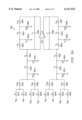
- each differential path receives its input through three sets of switches.
- switch pair 501 selectively input either VDD or GND in response to the output ⁇ of the delta-sigma modulator.
- switches 502a and 502b selectively input either VREF+ or VREF- to the lower path, depending again on the output ⁇ of the delta-sigma modulator.
- Switches 505a and 505b in turn switch the outputs of switch pairs 501 and 502 to sampling capacitor 403a in response to signals ⁇ 1DR and ⁇ 1DF respectively.
- Switches 506a and 506b perform the same function with regards to switch pairs 503 and 504 and sampling capacitor 403b.
- FIG. 5B is a diagram illustrating the relationship between signal ⁇ 1D and signals ⁇ 1DR (the initial or “rough” phase) and ⁇ 1DF (the “fine” phase).
- sampling capacitors (C S ) 403 are charged to either VDD or GND from the power supply.
- the power supply provides all of the DC charge needed to charge capacitors C S , plus some error charge due to power supply transients.
- the sampling capacitors C S are coupled to the reference voltages VREF+ and VREF- through switches 505b and 506b. Since capacitor 511 (see FIG.
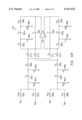
- FIG. 6A is a diagram of a further application of the present inventive principles in the switched capacitor section 600 of a delta-sigma DAC.
- the operation of circuitry 600 generally follows that of circuitry 500.
- a low-pass filter is included in each feedback loop, each of which includes switches 602 and 604 in series with reference capacitors (C r ) 603 and switches 605 and 606 in parallel with capacitors (C r ) 603.
- switches 602 and 604 in series with reference capacitors (C r ) 603 and switches 605 and 606 in parallel with capacitors (C r ) 603.
- switches 602 and 604 in series with reference capacitors (C r ) 603 and switches 605 and 606 in parallel with capacitors (C r ) 603.
- switches 505, 506 and 404 are charged by switches 505, 506 and 404.
- the existing charge on capacitors C r and C i is forced to the inputs of opamp 407 by switches 604 and 605.
- capacitors C i and C r are charged by the sampling capacitors C s and switches 406, 601, 602 and 606.
- FIG. 6B also is a diagram of the switched capacitor section 610 of a delta-sigma DAC.
- the reference voltage V ref is sampled by switches 607 and 608 onto sampling capacitors C s , independent of the value of delta, during ⁇ 1 .
- the charge on sampling capacitors C s is transferred to the summing node of opamp 407, with the direction of transfer controlled by delta through switches 611.
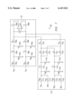
- ADC 700 of FIG. 7 An example of such a circuit is shown in the diagram of ADC 700 of FIG. 7.
- typical ADC circuitry is shown generally at 701. The operation of this circuit block is essentially as follows.
- ⁇ 1 the analog data at inputs Ain+ and Ain- are sampled by switches 702 and 704 on to the sampling capacitors 705.
- ⁇ 2 integration capacitors (C i ) 708 are charged by switches 706.
- the DAC circuitry 710 operates as follows. During ⁇ 1 , the reference voltage is sampled as described above by switches 711, 712 and 714. During ⁇ 2 , switches 713 and 716 transfer the charge on reference capacitors (C r ) 717 to the summing nodes of opamp integrator 707/708 through switches 715. Switches 715 control this charge transfer in response to the delta signal (i.e. the transfer is done in a data dependent fashion). A similar result can be achieved by a data-dependant sampling of the reference and a data independent transfer of the charge to the integrator.
- the present inventive concepts provide a simpler way of generating voltage references.
- This voltage reference scales with the value of the supply, which can enable circuit operation across a wide range of supplies. It consumes a minimal amount of power, and occupies very little on-chip area, without requiring expensive external components or compromising power-supply transient rejection.
Abstract
Circuitry for selectively sampling a reference voltage with a capacitor 403 includes a first switch 505a for selectively coupling capacitor 403 to a source of a first reference signal during a first operating phase and a second switch 505b for selectively coupling capacitor 403 to a source of a second reference signal during a second operating phase.
Description
1. Field of the Invention
The present invention relates in general to electronic circuits and in particular to reference voltage circuitry for use in switched-capacitor application and systems and methods using the same.
2. Description of the Related Art
The ability to process audio information has become increasingly important in the personal computer (PC) environment. Among other things, audio is important in many multimedia applications, such as gaming and telecommunications. Audio functionality is therefore typically available on most conventional PCS, either in the form of an add-on audio board or as a standard feature provided on the motherboard itself. In fact, PC users increasingly expect not only audio functionality but high quality sound capability.
One of the key components in most digital audio information processing systems is the Codec (coder-decoder) unit. Among other things, the Codec converts input analog audio information into a digital format for processing by a companion digital audio processor. The digital processor for example may support sample rate conversion, SoundBlaster compatibility, wavetable synthesis, or DirectSound acceleration, among other things. The Codec also converts outgoing signals from the audio processor from digital-to-analog format for eventual audible output to the user. The Codec may also mix analog and/or digital audio streams.
The digital to analog converters (DACs) and analog to digital converters (ADCs) found in a typical Codec operate from a reference voltage. Therefore, a reference voltage source must be provided whether it be external and coupled to the chip through a dedicated pin or on-chip, such as with a band gap reference. Even for inexpensive Codecs, the reference source must meet certain minimum criteria. Among other things, it must be small, low power consuming and have a good power supply rejection ratio (PSRR). Moreover, different DACs and ADCs often require the generation of different reference voltages. Therefore, the need has arisen for circuits and methods for generating reference voltages which not only meet the above performance criteria, but also allows for the scaling of the reference voltage with the DC value of the power supply voltage.
The principles of the present invention are embodied in circuitry for sampling a reference voltage with a capacitor and includes a first switch for selectively coupling the capacitor to a source of a first reference signal during a first operating phase and a second switch for selectively coupling the capacitor to a source of a second reference signal during a second operating phase. The principles of the present invention can be applied to a wide variety of circuitry which require charging of a capacitive load. Among other things, these principles allow for the scalable generation of a reference voltage as a function of a general power supply voltage. Notwithstanding, the principles of the present invention allow for the designing and fabrication of reference voltage generation circuitry which is small, low power consuming, and having a good power supply rejection ratio.
For a more complete understanding of the present invention, and the advantages thereof reference is now made to the following descriptions taken in conjunction with the accompanying drawings, in which:
FIG. 1A is a diagram of the major components of a mixed-signal serial Codec according to the principles of the present invention;
FIG. 1B is an overview diagram of the Codec of FIG. 1A, which includes individual definitions of the inputs and outputs;
FIG. 2 is a diagram the AC link connections between Codec and a digital audio controller;
FIG. 3 is a diagram of a representative embodiment of mixer of the Codec of FIGS. 1A and 1B;
FIG. 4A is a diagram of the typical switched-capacitor part of a delta-sigma digital to analog converter (DAC);
FIG. 4B is a diagram of the typical circuit used to generate the reference voltages required for the operation of the switched-capacitor circuitry of FIG. 4A;
FIG. 4C is a timing diagram illustrating the operation of the switched-capacitor circuitry of FIG. 4A;
FIG. 5A is a diagram of a switched-capacitor circuit for use in a digital-to-analog converter and embodying the principles of the present invention;
FIG. 5B is a timing diagram illustrating selected control signals used during the operation of the circuitry of FIG. 5A;
FIG. 5C is a diagram of circuitry for generating the reference voltages used during the operation of the circuitry of FIG. 5A in accordance with the present principles;
FIG. 6A is a diagram of additional exemplary switched-capacitor circuitry embodying the present principles and suitable for use in a delta-sigma DAC;
FIG. 6B is a diagram of an alternate configuration of the exemplary circuitry of FIG. 6A; and
FIG. 7 is a diagram of an exemplary analog to digital converter (ADC) embodying the present principles.
FIG. 1A is a diagram of the major components of a mixed-signal serial Codec 100. As discussed further below, when used in a system including a digital audio accelerator (controller), Codec 100 mixes analog data streams received from system-external sources and digital data streams received from the controller. Exemplary Codec 100 is also compliant with the Intel AC '97 specification, revision 1.03, Sep. 15, 1996, and will be described in that environment.
As shown in FIG. 1A, Codec 100 includes input port 101 for receiving data from four mono and four stereo analog input sources. Input multiplexer 102 selectively presents one of the analog inputs received at input port 101 to analog-to-digital converters (ADCs) 103. After conversion of the selected data stream from analog to a digital format, the stream is passed on to an audio Codec (AC) Link driver 104.
AC-Link driver 104 allows Codec 100 to communicate with a companion digital controller via a 5-wire serial link 105. In accordance with the AC '97 specification, serial link 105 consists of two clock lines, two data lines, and a reset line.
The output path of a Codec 100 includes digital-to-analog converters (DACs) 108, for transforming the digital data processed by AC-Link 104 into analog format, and an output mixer 106. Output mixer 106 presents to output port 107 a stereo output, on two lines, and a mono output on a single line. Signals output from output port 107 can then be recorded or delivered to audio components (amplifiers, speakers, etc.) for audible presentation to the user.
FIG. 1B is a more detailed overview diagram of Codec 100, which includes individual definitions of the inputs into input port 101, the lines of 5-wire serial link 105, and the outputs from output port 107. Further, FIG. 1B depicts selected internal data and control signals pertinent to the present discussion. FIG. 1B also generally shows the AC '97 registers 108, internal test circuitry 109 and power management circuitry 110.
As shown in FIG. 1B, the input port 101 is comprised of eight individual inputs, four single line (pin) inputs for receiving mono source information and four two line (pin) inputs for receiving stereo source information. The specific sources include LINE-- IN, AUX-- IN, VIDEO-- IN, MIC1-- IN, MIC2-- IN, PHONE, and PC-- BEEP.
The LINE-- IN pair of inputs provide for the input of left and right stereo analog data. The two AUX-- IN inputs provide left and right channel stereo analog auxiliary source input. The pair of inputs CD-- IN are used for the input of left and right channel CD audio analog data. The input pair labeled VIDEO-- IN is provided for inputting left and right channel stereo analog audio signal inputs from a video device.
Inputs MIC1-- IN and MIC2-- IN are multiplexed single inputs each of which can independently be used as a monophonic analog input source to output mixer 106. The selected input is also provided to input mixer 102. These inputs are in particular provided as alternate microphone connections.
The PHONE single-pin input provides for the input of data from a voice modem and therefore is not coupled to the stereo to mono mixer. The input (single-pin) labeled PC-- BEEP provides a PC-- BEEP connection to Codec 100. This input is also not coupled to the stereo to mono mixer.
5-Wire AC link 105 provides for the input of the synchronization (SYNC) signal, data from the controller (SD-- OUT) and reset signals, and for the output of the link clock (BIT-- CLK) and data to the controller(SD-- IN), in accordance with the AC '97 interface specification. These signals are best described in reference to FIG. 2.
FIG. 2 depicts the AC link connections between Codec 100 and an exemplary digital AC '97 controller 200. Controller 200 could be any controller conforming to the Intel AC '97 specification, such as a Crystal Semiconductor CS-4610 device configured as an AC '97 controller.
BIT-- CLK is the main clock which defines the protocol used on link 105 and in particular, is used by controller 200 to synchronize signals SYNC and SDATA-- OUT being passed back to Codec 100. The signal SYNC is generated by controller 100 and presented to Codec 100 to define the beginning of a frame of AC'97 audio data and is synchronous to the rising edge of BIT-- CLK.
The signal SDATA-- OUT (serial output data) is generated by controller 100 and input to Codec 100. Specifically, this data is positioned by controller 200 on the rising edge of BIT-- CLK and Codec 100 then samples this data on the falling edge of BIT-- CLK.
SDATA-- IN is used by controller 200 to receive serial data and status information from Codec 100. Specifically, Codec 100 positions data on the SDATA-- IN line on the rising edge of BIT-- CLK and controller 200 samples of the signal transferred on this line on the falling edge of BIT-- CLK. Reset signal RESET is generated by controller 200 and forces Codec 100 into power-up initialization.
Output port 107 includes an output pair LINE-- OUT, an ALT-- LINE-- OUT output pair and a single MONO-- OUT line. The primary output LINE-- OUT is available to drive the left and right channels of a stereo audio device, such as powered speakers 201 or similar audio loads. The alternate output (ALT-- LINE-- OUT), provides a connection to additional stereo audio devices or simply an optional stereo output. The MONO-- OUT line (pin) is the device monophonic audio, and finally, the PHONE output is provided to transfer data to a telephonic speakerphone, handset or headset.
FIG. 3 is a more detailed diagram of a first embodiment of the mixer 300A of Codec 100. The individual components/subsystems are controlled by the contents of corresponding registers within register 108.
Codec 100 includes multiple processing paths for mixing and converting data being exchanged between controller 200 and external analog audio devices. The Codec 100 data paths can generally be described as follows.
During the input of data to controller 200, selector 102 selects one stream from among a set of streams including the unmixed input analog streams (MIC1 or MIC2, LINE-- IN, CD, VIDEO and AUX-- IN). The selected stream, after conversion to a digital format, is transmitted to controller 200 via the SDATA-- IN line of link 105.
During the output of data streams from controller 200 to external audio devices, PCM data from controller 200 is input through SDATA-- OUT port and selectively mixed with the audio input streams (MIC1 or MIC2, LINE-- IN, CD, VIDEO or AUX-- IN), converted into analog format, and output to the given external audio devices via the LINE-- OUT, MONO-- OUT or ALT-- LINE-- OUT pins.
Codec 100 further includes a number of other selectable paths for processing flexibility.
In one input path, MIC1 or MIC2, LINE, CD, VIDEO and/or AUX inputs data presented at 101 are passed to input multiplexer 102 directly. Specifically, a switch 301 allows the user to select for input between data generated by microphone 1 (MIC1) and by microphone 2 (MIC2). The selected microphone input is then amplified by amplifier 302 by approximately +20 dB. The microphone analog data output from amplifier 302 is presented not only to the input of input multiplexer 102, but also through an amplifier 303 and a dedicated microphone analog-to-digital converter 304. The direct data path through amplifier 303 and ADC 304, when used, allows the transmission of PCM microphone data to controller 200 via the SDATA-- IN line.
The remaining signals, LINE, CD, VIDEO and/or AUX are provided directly to multiplexer 102. Multiplexer 102 can thus select directly from any one of the signals presented at input 101. Input multiplexer 102 has independent control of the left and right channels which advantageously facilitates returning a mono mix of the stereo line channel and/or echo cancellation on the microphone source by controller 200. In addition to selecting any one of the five analog input sources, such as the MIC, CD, LINE-- IN, VIDEO or AUX, presented at inputs 101, multiplexer 102 can also select from the stereo output mix or mono output mix.
The input stream selected by input multiplexer 102 is amplified by amplifier 305 which in turn drives main analog-to-digital converters (ADCs) 103. Each ADC is generally a delta-sigma (ΔΣ) converter. After analog-to-digital conversion, the two-line stereo input stream is passed through mute control circuitry 306 and on to digital mixer 307.
Mixer 307 is provided to mix the input signals selected by multiplexer 102 with mixed digital stereo data tapped from the stereo mixing section. The data received from the stereo mixing section by digital mixer 307 results from the mixing of PCM data received through the SDATA-- OUT line of AC'97 link 105 with the MIC1 or MIC2, LINE, CD, VIDEO or AUX inputs of input port 101 after passage through volume controls 308 and mute controls 309. Similarly, the PCM data from controller 200 is input through volume controls 310 and mute controls 311.
The analog inputs MIC1 or MIC2, LINE, CD, VIDEO or AUX are mixed by an analog stereo effect mixer 312 before conversion to digital format by effects path ADC 313. Additional mute controls 314 are provided at the output of ADC 313.
A digital mixer 315 selectively mixes the outputs of analog-to-digital converter 313 received from controller 200 through volume control 310 and mute control 311. If mixing of PCM data with the mixed and converted analog data from the analog inputs is not desired before 3-D processing, only the converted analog input data is passed through mixer 315. The digital mixed signal output from mixer 315 can optionally undergo 3-D audio processing by 3-D audio circuitry 316 or can bypass 3-D processing circuitry 316 through switch 317.
Another digital mixer 318 provides an optional path for mixing received data from controller 200 with the data input from inputs 101. In this case, the mixing of the data originally input as analog at inputs 101 is mixed with the digital data direct from controller 200 after optional 3-D processing by 3-D processing circuitry 316. In other words, 3-D processing for the PCM data can be selectively foregone, notwithstanding the fact that 3-D processing is performed on the converted analog input data. The output of mixer at 318 is then provided to tone controls 319. The two-channel output of tone controls 319 are passed through mute controls 320 and directly therefrom to digital mixer 307.
The two-channel output of tone control 319 is also provided to main digital-to-analog converters 106. The digital-to-analog converters (DACs) of Codec 100 may be, for example, delta-sigma converters. Analog output from main DAC converter 106 is passed through mute controls 321 and on to analog stereo output mixer 322. Analog stereo output mixer 322 mixes the analog signal output from main DAC 106 with the PC-- BEEP and PHONE inputs received from input port 101 (through volume controls 323a-323b and mute controls 324a-324b). Mixer 322 can also receive analog data directly from analog effects mixer 312 through a 90 dB analog bypass path. In particular, the analog bypass path takes analog data directly from analog stereo effects mixer 312, passes them through mute controls 325 and directly on to analog input mixer 322.
Mixed analog output data from analog mixer 322 provides a further input to input multiplexer 102. Most importantly, the output of analog stereo output mixer 322 passed to the LINE-- OUT and HP-- OUT outputs of Codec 100 output port 107 for transmission to external audio devices. The LINE-- OUT output is driven by master volume control 327 and output buffer 328 while the HP-- OUT output is driven by headphone volume control 329 and headphone driver 330.
The mono output (MONO-- OUT) is not directly generated from analog stereo mixer 322. Instead, a mono output mixer 326 mixes in the PC-- BEEP and PHONE sources with the PCM and analog sources. This scheme is advantageous, for example, because the mono mix from the mono output port may be used to drive a phone handset. Mixing the phone input back into the handset may cause echoes at the other end of the phone line. Therefore, the mono mix is taken from the analog input mixer 312 through the analog bypass, which does not include the PC-- BEEP or PHONE source signals.
For a complete description of Codec 100, refer to copending and co-assigned U.S. patent application, entitled CIRCUITS AND METHODS FOR IMPLEMENTING AUDIO CODEC AND SYSTEMS USING THE SAME, filed on Apr. 4, 1997 and the assigned Ser. No. 08/833,185, incorporated herein by reference.
FIG. 4A depicts a typical fully-differential switched-capacitor low-pass filter 400 found in delta-sigma DACs, such as DACs 106 discussed above. This design operates off the reference voltages VREF+ and VREF-.
A number of different means have been used to generate the reference voltages VREF+ and VREF-, including techniques which produce a voltage which is independent of supply voltage, temperature, process, and similar factors. It is also important to note the difference between the rejection of power supply transients and independence from the mean voltage of the power supply. Many applications require that both criteria be met while other applications only require that the reference produced not be disturbed by transients.
One technique for providing a reference voltage is to produce a bandgap voltage reference, where the difference in base-emitter voltage between two bipolar devices with different current densities is applied across a fixed resistor. Since this method produces a voltage which does not scale with the average value of the supply, operation across a wide supply range is difficult. Another approach is to provide a pin to allow use of a chip-external reference source. This however simply shifts the problem from the chip maker the system designer. For low cost applications, the inclusion of an additional component is a poor design choice. Instead, designers often just tie the reference pin to the power supply voltage and use a very large off-chip decoupling capacitor for filtering. However, to achieve a good PSRR at low frequencies, for example at 60 Hz, this capacitor would be prohibitively large.
A possible circuit for generating reference voltages to drive DAC circuitry 400 is shown in FIG. 4B. As will become apparent from a discussion of the operation of circuitry 400, this type of reference voltage source is alone not generally adequate for the task.
The one-bit output Δ of a delta-sigma modulator (not shown) is used to selectively switch the reference voltages VREF+ and VREF- to the two differential paths. Transistors 401a and 401b control the first path and transistors 402a and 402 the second path. The input voltages are then switched through circuitry 400 generally in accordance with the timing diagram of FIG. 4C.
When clock Φ1 is active (high), a first plate of each sampling capacitor (CS) 403a and 403b is connected the common mode voltage, Vcm, through switches 404a and 404b respectively. Then, when clock Φ1D, which is a delayed version of clock Φ1, closes switches 405a and 405b, charge is transferred to sampling capacitors 403a and 403b. If Δ is a logic high, then sampling capacitor 403a is charged to VREF+ and sampling capacitor 403b to VREF-. If Δ is a logic low, the opposite occurs.
Next, Φ1 opens switches 404a and 404b and a charge Qs =(VIN -VCM)CS is trapped on each sampling capacitor CS. Φ1D then returns low. Subsequently, clock Φ2 closes switches 406a and 406b and sampling capacitors CS are connected to corresponding inputs of operational amplifier 407. Clock Φ2D (the delayed version of Φ2) closes switches 408a and 408b thereby forcing charge QS from sampling capacitors 403a and 403b to integration capacitors (C1) 409a and 409b respectively.
Typically, a voltage reference source, such as source 410 shown in FIG. 4B includes a large value filtering resistor (RF) 411 and a small filtering capacitor (CF) 412 which produce in a low-pass filtered version of the power supply output. The values of resistor 411 and capacitor 412 are normally chosen to attenuate 60 Hz components output from the power supply to a satisfactory level. For example, if the pole frequency is chosen to be 0.6 Hz, the PSRR at 60 Hz is 40 dB. To keep the capacitor CF small, the resistor RF must be large. For a 1uF capacitor, the resistor would be about 250 kOhms. This circuit therefore has a significant disadvantage. Due to the large value of resistor RF, any current drawn from the filtered node 413 to charge CS will cause VREF to droop below VDD, which is undesirable. A buffer could be added between node 413 and the converter, but this would cost power and chip area and would be difficult to implement since VREF is substantially equal to the supply voltage VDD.
In the specific case of switched-capacitor circuitry 400, the following occurs when reference voltage source 401 or similar circuitry is used to supply the reference. As noted above, when Φ1D is active the reference voltage is sampled on to the sampling capacitors CS and therefore the reference source must be capable of charging the sampling capacitors to either VREF+ or VREF-. If the sampling frequency is fS, the switched capacitors CS each drain an amount of current from the reference voltage source equivalent to that drained by a resistor of value 1/(fs *CS). This causes the reference voltages VREF+ and VREF- to droop as described above.
The concepts of the present invention are best described in view of FIG. 5. In switched-capacitor circuit 500, each differential path receives its input through three sets of switches. For the upper path, switch pair 501 selectively input either VDD or GND in response to the output Δ of the delta-sigma modulator. At the same time, switches 502a and 502b selectively input either VREF+ or VREF- to the lower path, depending again on the output Δ of the delta-sigma modulator. Switches 505a and 505b in turn switch the outputs of switch pairs 501 and 502 to sampling capacitor 403a in response to signals Φ1DR and Φ1DF respectively. Switches 506a and 506b perform the same function with regards to switch pairs 503 and 504 and sampling capacitor 403b.
FIG. 5B is a diagram illustrating the relationship between signal Φ1D and signals Φ1DR (the initial or "rough" phase) and Φ1DF (the "fine" phase). During the "rough" phase, sampling capacitors (CS) 403 are charged to either VDD or GND from the power supply. The power supply provides all of the DC charge needed to charge capacitors CS, plus some error charge due to power supply transients. During the "fine" phase, the sampling capacitors CS are coupled to the reference voltages VREF+ and VREF- through switches 505b and 506b. Since capacitor 511 (see FIG. 5C) is relatively large in comparison to the sampling capacitors CS, the voltage errors on the sampling capacitors are reduced by their ratios with capacitor 115, thereby eliminating any error charge on the sampling capacitors. Since all the DC charge is provided during the "rough" phase from the power supply, the VREF nodes do not droop.
FIG. 5C depicts one technique for generating the reference voltages used in FIG. 5A. Here, the relevant portion of a chip 507 is shown, including bondpads 508 and on-chip resistors 509a and 509b. Externally, the corresponding bondwires 510 and off-chip capacitors 511 and 512 are shown. Initial theory suggests that an external resistor 512 (shown in dashed lines) is required provide charge to capacitor 511. Surprisingly however, experimental results have shown that resistor 512 is not needed at all. Analysis reveals that this benefit results from the fact that when the sampling capacitors CS are coupled to the filter capacitor CFIL 511, they have already been charged to VDD. Input from the power supply is still filtered, with a pole at Fpole =1/2πFS ·CS /CFIL or about 0.5 Hz. Preferably, provisions are made to quickly charge capacitor CFIL at startup.
FIG. 6A is a diagram of a further application of the present inventive principles in the switched capacitor section 600 of a delta-sigma DAC. The operation of circuitry 600 generally follows that of circuitry 500. In this case, however, a low-pass filter is included in each feedback loop, each of which includes switches 602 and 604 in series with reference capacitors (Cr) 603 and switches 605 and 606 in parallel with capacitors (Cr) 603. During Φ1 sampling capacitors Cs are charged by switches 505, 506 and 404. The existing charge on capacitors Cr and Ci is forced to the inputs of opamp 407 by switches 604 and 605. During Φ2, capacitors Ci and Cr are charged by the sampling capacitors Cs and switches 406, 601, 602 and 606. Capacitors Ci and Cr implement a low-pass filter with a pole at Fpole =Fs *Cr /Cs, where Fpole is the pole frequency and Fs is the sampling frequency.
A similar approach is depicted in FIG. 6B, which also is a diagram of the switched capacitor section 610 of a delta-sigma DAC. Here, the reference voltage Vref is sampled by switches 607 and 608 onto sampling capacitors Cs, independent of the value of delta, during Φ1. Then, during Φ2, the charge on sampling capacitors Cs is transferred to the summing node of opamp 407, with the direction of transfer controlled by delta through switches 611.
In many delta-sigma ADCs, there is a switched-capacitor DAC incorporated in the reference feedback loop. An example of such a circuit is shown in the diagram of ADC 700 of FIG. 7. Here, typical ADC circuitry is shown generally at 701. The operation of this circuit block is essentially as follows. During Φ1, the analog data at inputs Ain+ and Ain- are sampled by switches 702 and 704 on to the sampling capacitors 705. During Φ2, integration capacitors (Ci) 708 are charged by switches 706.
The DAC circuitry 710 operates as follows. During Φ1, the reference voltage is sampled as described above by switches 711, 712 and 714. During Φ2, switches 713 and 716 transfer the charge on reference capacitors (Cr) 717 to the summing nodes of opamp integrator 707/708 through switches 715. Switches 715 control this charge transfer in response to the delta signal (i.e. the transfer is done in a data dependent fashion). A similar result can be achieved by a data-dependant sampling of the reference and a data independent transfer of the charge to the integrator.
In sum, the present inventive concepts provide a simpler way of generating voltage references. This voltage reference scales with the value of the supply, which can enable circuit operation across a wide range of supplies. It consumes a minimal amount of power, and occupies very little on-chip area, without requiring expensive external components or compromising power-supply transient rejection.
Although the present invention and its advantages have been described in detail, it should be understood that various changes, substitutions and alterations can be made herein without departing from the spirit and scope of the invention as defined by the appended claims.
Claims (19)
1. Circuitry for sampling a reference voltage with a capacitor comprising:
a first switch for selectively coupling the capacitor to a voltage supply rail sourcing a first reference signal during a first operating phase; and
a second switch for selectively coupling the capacitor to a second capacitor to generate a second reference signal during a second operating phase, the second reference signal comprising the first reference signal filtered for AC noise.
2. The circuitry of claim 1 wherein the first and second reference signals have a voltage selected to be approximately equal to a power supply voltage in response to a first state of a control signal.
3. The circuitry of claim 2 wherein the first reference and second reference signals have a voltage selected to be approximately zero volts in response to a second state of the control signal.
4. The circuitry of claim 3 wherein the control signal is generated by a delta-sigma modulator.
5. The circuitry of claim 1 wherein said capacitor comprises a sampling capacitor in a digital to analog converter.
6. The circuitry of claim 1 wherein said capacitor comprises a sampling capacitor in an analog to digital converter.
7. Circuitry for generating a reference voltage comprising:
a first switch for sampling a first reference voltage onto a first capacitor during a first operating phase; and
a second switch for coupling charge from a second capacitor to the first capacitor during a second operating phase.
8. The circuitry of claim 7 wherein the second capacitor is substantially larger than the first capacitor.
9. The circuitry of claim 7 and further comprising a resistor coupling the second capacitor with the first reference voltage.
10. The circuitry of claim 7 wherein the first reference voltage comprises a chip supply voltage.
11. A method for sampling a voltage in switched capacitor circuitry comprising the steps of:
during a first operating phase, coupling a sampling capacitor to a source of a unfiltered reference voltage; and
during a second operating phase, coupling the sampling capacitor to a source of a filtered reference voltage.
12. The method of claim 11 and further comprising the step of selecting the source of the unfiltered voltage between a positive voltage source and ground in response output from a delta-sigma modulator.
13. The method of claim 11 and further comprising the step generating the filtered reference voltage by filtering the unfiltered reference voltage.
14. The method of claim 13 wherein said step of coupling the sampling capacitor to a source of a filtered reference voltage comprises the substeps of:
charging a second capacitor through a resistor from the source of the unfiltered voltage, the second capacitor being substantially larger than the sampling capacitor; and
coupling the second capacitor with the sampling capacitor.
15. An audio data processing device comprising:
a data converter including switched-capacitor circuitry, said switched capacitor circuitry comprising:
a sampling capacitor;
a first switching circuit for selectively roughly charging said sampling capacitor with a voltage supplied by a voltage supply rail;
and
a second switching circuit for selectively finely charging said sampling capacitor, said second switching circuitry coupling said sampling capacitor to a filtering capacitor to filter said voltage supplied by said voltage supply rail for AC noise.
16. The audio data processing device of claim 15 wherein said converter comprises a digital to analog converter.
17. The audio data processing device of claim 15 wherein said converter comprises an analog to digital converter.
18. The audio data processing device of claim 15 and further comprising a delta-sigma modulator for generating a signal controlling third switching circuitry for selectively switching a selected one of a plurality of voltage supply rails to said first switching circuitry.
19. The audio data processing of claim 15 and further comprising a delta-sigma modulator for generating a signal controlling third switching circuitry for selectively switching a selected one of a plurality of signals generated by filtering a selected one of plurality of voltage rail voltages to said second switching circuitry.
Priority Applications (1)
| Application Number | Priority Date | Filing Date | Title |
|---|---|---|---|
| US09/224,390 US6147522A (en) | 1998-12-31 | 1998-12-31 | Reference voltage circuitry for use in switched-capacitor applications |
Applications Claiming Priority (1)
| Application Number | Priority Date | Filing Date | Title |
|---|---|---|---|
| US09/224,390 US6147522A (en) | 1998-12-31 | 1998-12-31 | Reference voltage circuitry for use in switched-capacitor applications |
Publications (1)
| Publication Number | Publication Date |
|---|---|
| US6147522A true US6147522A (en) | 2000-11-14 |
Family
ID=22840468
Family Applications (1)
| Application Number | Title | Priority Date | Filing Date |
|---|---|---|---|
| US09/224,390 Expired - Lifetime US6147522A (en) | 1998-12-31 | 1998-12-31 | Reference voltage circuitry for use in switched-capacitor applications |
Country Status (1)
| Country | Link |
|---|---|
| US (1) | US6147522A (en) |
Cited By (41)
| Publication number | Priority date | Publication date | Assignee | Title |
|---|---|---|---|---|
| US6389033B1 (en) * | 1999-01-25 | 2002-05-14 | Conexant Systems, Inc. | System and method for performing signal acceleration on an AC link bus |
| US6617908B1 (en) * | 2002-03-22 | 2003-09-09 | Cirrus Logic, Inc. | Switched-capacitor circuits with reduced distortion |
| US6628217B1 (en) * | 2001-07-27 | 2003-09-30 | Cypress Semiconductor Corp. | Signal scaling scheme for a delta sigma modulator |
| US6636084B2 (en) * | 1999-12-22 | 2003-10-21 | Texas Instruments Incorporated | Sample and hold circuit |
| US20040051557A1 (en) * | 2002-09-12 | 2004-03-18 | Kim Yong-Ki | Input buffer of differential amplification type in semiconductor device |
| US20040165669A1 (en) * | 2003-02-21 | 2004-08-26 | Kanji Otsuka | Signal transmission apparatus and interconnection structure |
| US20040210801A1 (en) * | 2003-04-16 | 2004-10-21 | Cirrus Logic, Inc. | Sample and hold circuits and methods with offset error correction and systems using the same |
| US20050134368A1 (en) * | 2003-12-19 | 2005-06-23 | Chandrasekaran Ramesh M. | Switching scheme to improve linearity and noise in switched capacitor stage with switched feedback capacitor |
| US20050212591A1 (en) * | 2004-03-23 | 2005-09-29 | Microchip Technology Incorporated | Switched capacitor signal scaling circuit |
| US6956519B1 (en) * | 2004-10-11 | 2005-10-18 | Faraday Technology Corp. | Switched capacitor circuit of a pipeline analog to digital converter and a method for operating the switched capacitor circuit |
| US6965333B1 (en) * | 2005-04-12 | 2005-11-15 | Princeton Technology Corporation | Circuit for using capacitor voltage divider in a delta-sigma digital-to-analog converter to generate reference voltage |
| EP1635468A1 (en) * | 2004-09-10 | 2006-03-15 | Cirrus Logic, Inc. | Single ended switched capacitor circuit |
| US20060055576A1 (en) * | 2004-08-25 | 2006-03-16 | Christian Boemler | Analog to digital conversion with offset cancellation |
| US7015852B1 (en) | 2004-11-30 | 2006-03-21 | Freescale Semiconductor, Inc. | Cyclic analog-to-digital converter |
| US20060119501A1 (en) * | 2004-12-03 | 2006-06-08 | Integration Associates Inc. | Multiplexed voltage reference strategy for codec |
| US7102557B1 (en) * | 2005-04-19 | 2006-09-05 | Wolfson Microelectronics Plc | Switched capacitor DAC |
| US20060255854A1 (en) * | 2005-05-12 | 2006-11-16 | Ahuja Bhupendra K | Precision floating gate reference temperature coefficient compensation circuit and method |
| US20070030037A1 (en) * | 2005-08-02 | 2007-02-08 | Wen-Chi Wang | Reference voltage generating circuit |
| US7183954B1 (en) * | 2001-07-13 | 2007-02-27 | Cirrus Logic, Inc. | Circuits, systems and methods for volume control in low noise 1-bit digital audio systems |
| US20070046523A1 (en) * | 2005-08-30 | 2007-03-01 | Wen-Chi Wang | Reference voltage generating circuit |
| US20070103203A1 (en) * | 2005-11-08 | 2007-05-10 | Denso Corporation | Sample hold circuit and multiplying D/A converter having the same |
| US20070275684A1 (en) * | 2006-05-24 | 2007-11-29 | Hiroyuki Harada | Mixer having frequency selection function |
| US7417462B1 (en) * | 2007-03-20 | 2008-08-26 | Altera Corporation | Variable external interface circuitry on programmable logic device integrated circuits |
| US20080238492A1 (en) * | 2007-03-30 | 2008-10-02 | Budiyanto Junus | Slew-rate detection circuit using switched-capacitor comparators |
| US20080258826A1 (en) * | 2004-09-20 | 2008-10-23 | The Trustees Of Columbia University In The City Of New York | Low Voltage Operational Transconductance Amplifier Circuits |
| US20090102517A1 (en) * | 2007-10-17 | 2009-04-23 | Agilent Technologies, Inc. | Track-And-Hold Circuit With Adjustable Charge Compensation |
| US20090170466A1 (en) * | 2007-12-31 | 2009-07-02 | Industrial Technology Research Institute | Circuit with programmable signal bandwidth and method thereof |
| US20100219864A1 (en) * | 2009-02-27 | 2010-09-02 | Atmel Corporation | Dual Mode, Single Ended to Fully Differential Converter Structure |
| US20100264751A1 (en) * | 2009-04-21 | 2010-10-21 | Sachio Iida | Filter circuit and communication apparatus |
| US7948270B1 (en) * | 2009-12-29 | 2011-05-24 | Cadence Design Systems, Inc. | System and method for level translation in serial data interface |
| US20110279148A1 (en) * | 2010-05-14 | 2011-11-17 | Hikaru Watanabe | Sample and hold circuit and a/d converter apparatus |
| JP2012227622A (en) * | 2011-04-15 | 2012-11-15 | Toyota Motor Corp | Digital/analog-mixed circuit and digital clock generation circuit |
| US8552788B2 (en) * | 2011-09-15 | 2013-10-08 | Analog Devices, Inc. | Apparatus and methods for adaptive common-mode level shifting |
| CN105811989A (en) * | 2016-02-24 | 2016-07-27 | 芯海科技(深圳)股份有限公司 | Integrator gain multiplication circuit applied to sigma-delta modulator |
| US9444489B2 (en) | 2014-11-24 | 2016-09-13 | Samsung Electronics Co., Ltd. | Delta-sigma modulator having differential output |
| US9557759B2 (en) | 2014-01-09 | 2017-01-31 | Samsung Electronics Co., Ltd. | Reference voltage generator |
| CN107332525A (en) * | 2017-08-01 | 2017-11-07 | 深圳市中移联半导体科技有限公司 | A kind of superelevation PSRR power amplification device |
| US11115042B1 (en) * | 2020-10-09 | 2021-09-07 | Beken Corporation | Low pass filter embedded digital-to-analog converter |
| US20220149864A1 (en) * | 2020-11-12 | 2022-05-12 | Cirrus Logic International Semiconductor, Ltd. | Gain error reduction in switched-capacitor delta-sigma data converters sharing a voltage reference with a disabled data converter |
| TWI774289B (en) * | 2021-03-25 | 2022-08-11 | 瑞昱半導體股份有限公司 | Audio mixing device and audio mixing method |
| US11483654B2 (en) * | 2020-02-10 | 2022-10-25 | Cirrus Logic, Inc. | Driver circuitry |
Citations (4)
| Publication number | Priority date | Publication date | Assignee | Title |
|---|---|---|---|---|
| US4546324A (en) * | 1982-12-27 | 1985-10-08 | Intersil, Inc. | Digitally switched analog signal conditioner |
| US5506526A (en) * | 1992-02-21 | 1996-04-09 | Sierra Semiconductor B.V. | Offset-compensated sample and hold arrangement and method for its operation |
| US5635864A (en) * | 1995-06-07 | 1997-06-03 | Discovision Associates | Comparator circuit |
| US5644257A (en) * | 1993-03-24 | 1997-07-01 | Crystal Semiconductor Corporation | Sampling circuit charge management |
-
1998
- 1998-12-31 US US09/224,390 patent/US6147522A/en not_active Expired - Lifetime
Patent Citations (4)
| Publication number | Priority date | Publication date | Assignee | Title |
|---|---|---|---|---|
| US4546324A (en) * | 1982-12-27 | 1985-10-08 | Intersil, Inc. | Digitally switched analog signal conditioner |
| US5506526A (en) * | 1992-02-21 | 1996-04-09 | Sierra Semiconductor B.V. | Offset-compensated sample and hold arrangement and method for its operation |
| US5644257A (en) * | 1993-03-24 | 1997-07-01 | Crystal Semiconductor Corporation | Sampling circuit charge management |
| US5635864A (en) * | 1995-06-07 | 1997-06-03 | Discovision Associates | Comparator circuit |
Cited By (74)
| Publication number | Priority date | Publication date | Assignee | Title |
|---|---|---|---|---|
| US6389033B1 (en) * | 1999-01-25 | 2002-05-14 | Conexant Systems, Inc. | System and method for performing signal acceleration on an AC link bus |
| US6636084B2 (en) * | 1999-12-22 | 2003-10-21 | Texas Instruments Incorporated | Sample and hold circuit |
| US7183954B1 (en) * | 2001-07-13 | 2007-02-27 | Cirrus Logic, Inc. | Circuits, systems and methods for volume control in low noise 1-bit digital audio systems |
| US6628217B1 (en) * | 2001-07-27 | 2003-09-30 | Cypress Semiconductor Corp. | Signal scaling scheme for a delta sigma modulator |
| US6617908B1 (en) * | 2002-03-22 | 2003-09-09 | Cirrus Logic, Inc. | Switched-capacitor circuits with reduced distortion |
| US20040051557A1 (en) * | 2002-09-12 | 2004-03-18 | Kim Yong-Ki | Input buffer of differential amplification type in semiconductor device |
| US6812743B2 (en) * | 2002-09-12 | 2004-11-02 | Hynix Semiconductor Inc. | Input buffer of differential amplification type in semiconductor device |
| US20040165669A1 (en) * | 2003-02-21 | 2004-08-26 | Kanji Otsuka | Signal transmission apparatus and interconnection structure |
| US7446567B2 (en) * | 2003-02-21 | 2008-11-04 | Kanji Otsuka | Signal transmission apparatus and interconnection structure |
| US20040210801A1 (en) * | 2003-04-16 | 2004-10-21 | Cirrus Logic, Inc. | Sample and hold circuits and methods with offset error correction and systems using the same |
| WO2004095512A3 (en) * | 2003-04-16 | 2006-01-05 | Cirrus Logic Inc | Sample and hold circuits and methods with offset error correction and systems using the same |
| US7088147B2 (en) * | 2003-04-16 | 2006-08-08 | Cirrus Logic, Inc. | Sample and hold circuits and methods with offset error correction and systems using the same |
| US20050134368A1 (en) * | 2003-12-19 | 2005-06-23 | Chandrasekaran Ramesh M. | Switching scheme to improve linearity and noise in switched capacitor stage with switched feedback capacitor |
| US6970038B2 (en) * | 2003-12-19 | 2005-11-29 | Texas Instruments Incorporated | Switching scheme to improve linearity and noise in switched capacitor stage with switched feedback capacitor |
| WO2005096505A1 (en) * | 2004-03-23 | 2005-10-13 | Microchip Technology Incorporated | Switched capacitor signal scaling circuit |
| US7046046B2 (en) | 2004-03-23 | 2006-05-16 | Microchip Technology Incorporated | Switched capacitor signal scaling circuit |
| US20050212591A1 (en) * | 2004-03-23 | 2005-09-29 | Microchip Technology Incorporated | Switched capacitor signal scaling circuit |
| US20060055576A1 (en) * | 2004-08-25 | 2006-03-16 | Christian Boemler | Analog to digital conversion with offset cancellation |
| US7061413B2 (en) * | 2004-08-25 | 2006-06-13 | Micron Technology, Inc. | Analog to digital conversion with offset cancellation |
| EP1635468A1 (en) * | 2004-09-10 | 2006-03-15 | Cirrus Logic, Inc. | Single ended switched capacitor circuit |
| US20060055436A1 (en) * | 2004-09-10 | 2006-03-16 | Gaboriau Johann G | Single ended switched capacitor circuit |
| US7477079B2 (en) | 2004-09-10 | 2009-01-13 | Cirrus Logic, Inc. | Single ended switched capacitor circuit |
| US20080258826A1 (en) * | 2004-09-20 | 2008-10-23 | The Trustees Of Columbia University In The City Of New York | Low Voltage Operational Transconductance Amplifier Circuits |
| US8305247B2 (en) | 2004-09-20 | 2012-11-06 | The Trustees Of Columbia University In The City Of New York | Low voltage digital to analog converter, comparator and sigma-delta modulator circuits |
| US8441287B2 (en) * | 2004-09-20 | 2013-05-14 | The Trustees Of Columbia University In The City Of New York | Low voltage track and hold circuits |
| US8704553B2 (en) | 2004-09-20 | 2014-04-22 | The Trustees Of Columbia University In The City Of New York | Low voltage comparator circuits |
| US20090303094A1 (en) * | 2004-09-20 | 2009-12-10 | The Trustees Of Columbia University In The City Of New York | Low voltage digital to analog converter, comparator and sigma-delta modulator circuits |
| US20090015329A1 (en) * | 2004-09-20 | 2009-01-15 | Shouri Chatterjee | Low Voltage Track and Hold Circuits |
| US8030999B2 (en) | 2004-09-20 | 2011-10-04 | The Trustees Of Columbia University In The City Of New York | Low voltage operational transconductance amplifier circuits |
| US6956519B1 (en) * | 2004-10-11 | 2005-10-18 | Faraday Technology Corp. | Switched capacitor circuit of a pipeline analog to digital converter and a method for operating the switched capacitor circuit |
| US7015852B1 (en) | 2004-11-30 | 2006-03-21 | Freescale Semiconductor, Inc. | Cyclic analog-to-digital converter |
| US7164377B2 (en) * | 2004-12-03 | 2007-01-16 | Integration Associates Inc. | Multiplexed voltage reference strategy for codec |
| US20060119501A1 (en) * | 2004-12-03 | 2006-06-08 | Integration Associates Inc. | Multiplexed voltage reference strategy for codec |
| US6965333B1 (en) * | 2005-04-12 | 2005-11-15 | Princeton Technology Corporation | Circuit for using capacitor voltage divider in a delta-sigma digital-to-analog converter to generate reference voltage |
| US7102557B1 (en) * | 2005-04-19 | 2006-09-05 | Wolfson Microelectronics Plc | Switched capacitor DAC |
| US20060255854A1 (en) * | 2005-05-12 | 2006-11-16 | Ahuja Bhupendra K | Precision floating gate reference temperature coefficient compensation circuit and method |
| US7221209B2 (en) | 2005-05-12 | 2007-05-22 | Intersil Americas, Inc | Precision floating gate reference temperature coefficient compensation circuit and method |
| US20070030037A1 (en) * | 2005-08-02 | 2007-02-08 | Wen-Chi Wang | Reference voltage generating circuit |
| US7456769B2 (en) | 2005-08-02 | 2008-11-25 | Realtek Semiconductor Corp. | Reference voltage generating circuit |
| US7253764B2 (en) | 2005-08-30 | 2007-08-07 | Realtek Semiconductor Corp. | Reference voltage generating circuit |
| US20070046523A1 (en) * | 2005-08-30 | 2007-03-01 | Wen-Chi Wang | Reference voltage generating circuit |
| US20070103203A1 (en) * | 2005-11-08 | 2007-05-10 | Denso Corporation | Sample hold circuit and multiplying D/A converter having the same |
| US7397287B2 (en) * | 2005-11-08 | 2008-07-08 | Denso Corporation | Sample hold circuit and multiplying D/A converter having the same |
| US7671658B2 (en) * | 2006-05-24 | 2010-03-02 | Panasonic Corporation | Mixer having frequency selection function |
| US20070275684A1 (en) * | 2006-05-24 | 2007-11-29 | Hiroyuki Harada | Mixer having frequency selection function |
| US7659745B1 (en) * | 2007-03-20 | 2010-02-09 | Altera Corporation | Variable external interface circuitry on programmable logic device integrated circuits |
| US7417462B1 (en) * | 2007-03-20 | 2008-08-26 | Altera Corporation | Variable external interface circuitry on programmable logic device integrated circuits |
| US7479810B2 (en) * | 2007-03-30 | 2009-01-20 | Intel Corporation | Slew-rate detection circuit using switched-capacitor comparators |
| US20080238492A1 (en) * | 2007-03-30 | 2008-10-02 | Budiyanto Junus | Slew-rate detection circuit using switched-capacitor comparators |
| US20090102517A1 (en) * | 2007-10-17 | 2009-04-23 | Agilent Technologies, Inc. | Track-And-Hold Circuit With Adjustable Charge Compensation |
| US7834665B2 (en) * | 2007-10-17 | 2010-11-16 | Agilent Technologies, Inc. | Track-and-hold circuit with adjustable charge compensation |
| US20090170466A1 (en) * | 2007-12-31 | 2009-07-02 | Industrial Technology Research Institute | Circuit with programmable signal bandwidth and method thereof |
| US7962115B2 (en) * | 2007-12-31 | 2011-06-14 | Industrial Technology Research Institute | Circuit with programmable signal bandwidth and method thereof |
| US20100219864A1 (en) * | 2009-02-27 | 2010-09-02 | Atmel Corporation | Dual Mode, Single Ended to Fully Differential Converter Structure |
| US7843232B2 (en) * | 2009-02-27 | 2010-11-30 | Atmel Corporation | Dual mode, single ended to fully differential converter structure |
| US8633617B2 (en) * | 2009-04-21 | 2014-01-21 | Sony Corporation | Filter circuit and communication apparatus |
| US20100264751A1 (en) * | 2009-04-21 | 2010-10-21 | Sachio Iida | Filter circuit and communication apparatus |
| US7948270B1 (en) * | 2009-12-29 | 2011-05-24 | Cadence Design Systems, Inc. | System and method for level translation in serial data interface |
| US8368430B2 (en) * | 2010-05-14 | 2013-02-05 | Toyota Jidosha Kabushiki Kaisha | Sample and hold circuit and A/D converter apparatus |
| US20110279148A1 (en) * | 2010-05-14 | 2011-11-17 | Hikaru Watanabe | Sample and hold circuit and a/d converter apparatus |
| JP2012227622A (en) * | 2011-04-15 | 2012-11-15 | Toyota Motor Corp | Digital/analog-mixed circuit and digital clock generation circuit |
| TWI561000B (en) * | 2011-09-15 | 2016-12-01 | Analog Devices Inc | Apparatus and methods for adaptive common-mode level shifting |
| US8552788B2 (en) * | 2011-09-15 | 2013-10-08 | Analog Devices, Inc. | Apparatus and methods for adaptive common-mode level shifting |
| CN103797711A (en) * | 2011-09-15 | 2014-05-14 | 美国亚德诺半导体公司 | Apparatus and methods for adaptive common mode level shifting |
| CN103797711B (en) * | 2011-09-15 | 2016-09-28 | 美国亚德诺半导体公司 | Equipment and method for the conversion of self adaptation common mode electrical level |
| US9557759B2 (en) | 2014-01-09 | 2017-01-31 | Samsung Electronics Co., Ltd. | Reference voltage generator |
| US9444489B2 (en) | 2014-11-24 | 2016-09-13 | Samsung Electronics Co., Ltd. | Delta-sigma modulator having differential output |
| CN105811989A (en) * | 2016-02-24 | 2016-07-27 | 芯海科技(深圳)股份有限公司 | Integrator gain multiplication circuit applied to sigma-delta modulator |
| CN107332525A (en) * | 2017-08-01 | 2017-11-07 | 深圳市中移联半导体科技有限公司 | A kind of superelevation PSRR power amplification device |
| US11483654B2 (en) * | 2020-02-10 | 2022-10-25 | Cirrus Logic, Inc. | Driver circuitry |
| US11115042B1 (en) * | 2020-10-09 | 2021-09-07 | Beken Corporation | Low pass filter embedded digital-to-analog converter |
| US20220149864A1 (en) * | 2020-11-12 | 2022-05-12 | Cirrus Logic International Semiconductor, Ltd. | Gain error reduction in switched-capacitor delta-sigma data converters sharing a voltage reference with a disabled data converter |
| US11777517B2 (en) * | 2020-11-12 | 2023-10-03 | Cirrus Logic, Inc. | Gain error reduction in switched-capacitor delta-sigma data converters sharing a voltage reference with a disabled data converter |
| TWI774289B (en) * | 2021-03-25 | 2022-08-11 | 瑞昱半導體股份有限公司 | Audio mixing device and audio mixing method |
Similar Documents
| Publication | Publication Date | Title |
|---|---|---|
| US6147522A (en) | Reference voltage circuitry for use in switched-capacitor applications | |
| US5864811A (en) | Audio circuit for use with synthesized audio signals and signals from a modem | |
| US6259957B1 (en) | Circuits and methods for implementing audio Codecs and systems using the same | |
| US6011501A (en) | Circuits, systems and methods for processing data in a one-bit format | |
| US10504526B2 (en) | Wireless cellular telephone with audio codec | |
| US7885422B2 (en) | Audio device and method | |
| US7376778B2 (en) | Audio device | |
| JP4747199B2 (en) | Architecture using digital / analog converter and low-pass filter with continuous time stage and switched capacitor stage | |
| Gata et al. | A 1.1-V 270-/spl mu/A mixed-signal hearing aid chip | |
| US5363102A (en) | Offset-insensitive switched-capacitor gain stage | |
| US6642876B2 (en) | Method and system of operating a codec in an operational mode | |
| US7162029B2 (en) | Gain or input volume controller and method utilizing a modified R2R ladder network | |
| US6522278B1 (en) | Digital-to-analog converter with power up/down transient suppression and automatic rate switching | |
| US7224756B2 (en) | Method and system for providing a codec clock signal at a desired operational rate | |
| US7003682B2 (en) | Power management method for setting clock circuit into power down mode if analog front end circuit is sampling input signals in an electronic device | |
| US20020057809A1 (en) | Reduced complexity audio mixing apparatus | |
| TWI774289B (en) | Audio mixing device and audio mixing method | |
| EP3940960A1 (en) | Efficient digital gain implementation in digital microphones | |
| US11659329B2 (en) | Efficient seamless switching of sigma-delta modulators | |
| US7248186B1 (en) | Noise management method and circuits suitable for utilization in circuits and systems having a switched data port | |
| Liepold et al. | An ASIC mixed-mode analog front end | |
| Becker et al. | A high-quality mixed-signal audio codec in 65-nm CMOS | |
| US20020177915A1 (en) | Audio amplifier circuit with digital audio interface and codec device using the same | |
| CN117155392A (en) | Digital-to-analog conversion system with multiple working modes and design method thereof | |
| Kim et al. | A 2.4 V, 12 mW stereo audio D/A converter with double sampling switching |
Legal Events
| Date | Code | Title | Description |
|---|---|---|---|
| AS | Assignment |
Owner name: CIRRUS LOGIC, INC., CALIFORNIA Free format text: ASSIGNMENT OF ASSIGNORS INTEREST;ASSIGNORS:RHODE, JASON POWELL;SRINIVASAN, VISHNU SHANKAR;GAALAAS, ERIC CLAY;AND OTHERS;REEL/FRAME:009853/0070 Effective date: 19990322 |
|
| STCF | Information on status: patent grant |
Free format text: PATENTED CASE |
|
| FPAY | Fee payment |
Year of fee payment: 4 |
|
| FPAY | Fee payment |
Year of fee payment: 8 |
|
| FPAY | Fee payment |
Year of fee payment: 12 |