US6147879A - Assemblies of electrical devices and flexible containers therefor - Google Patents
Assemblies of electrical devices and flexible containers therefor Download PDFInfo
- Publication number
- US6147879A US6147879A US08/989,719 US98971997A US6147879A US 6147879 A US6147879 A US 6147879A US 98971997 A US98971997 A US 98971997A US 6147879 A US6147879 A US 6147879A
- Authority
- US
- United States
- Prior art keywords
- container
- carrier
- chamber
- aperture
- laminate construction
- Prior art date
- Legal status (The legal status is an assumption and is not a legal conclusion. Google has not performed a legal analysis and makes no representation as to the accuracy of the status listed.)
- Expired - Fee Related
Links
Images


Classifications
-
- H—ELECTRICITY
- H05—ELECTRIC TECHNIQUES NOT OTHERWISE PROVIDED FOR
- H05K—PRINTED CIRCUITS; CASINGS OR CONSTRUCTIONAL DETAILS OF ELECTRIC APPARATUS; MANUFACTURE OF ASSEMBLAGES OF ELECTRICAL COMPONENTS
- H05K9/00—Screening of apparatus or components against electric or magnetic fields
- H05K9/0073—Shielding materials
- H05K9/0081—Electromagnetic shielding materials, e.g. EMI, RFI shielding
- H05K9/0084—Electromagnetic shielding materials, e.g. EMI, RFI shielding comprising a single continuous metallic layer on an electrically insulating supporting structure, e.g. metal foil, film, plating coating, electro-deposition, vapour-deposition
-
- H—ELECTRICITY
- H05—ELECTRIC TECHNIQUES NOT OTHERWISE PROVIDED FOR
- H05K—PRINTED CIRCUITS; CASINGS OR CONSTRUCTIONAL DETAILS OF ELECTRIC APPARATUS; MANUFACTURE OF ASSEMBLAGES OF ELECTRICAL COMPONENTS
- H05K9/00—Screening of apparatus or components against electric or magnetic fields
- H05K9/0007—Casings
- H05K9/0043—Casings being flexible containers, e.g. pouch, pocket, bag
Definitions
- This invention relates to electronic devices within flexible containers.
- a problem with the construction described in the above patent is that the connector body needs to be sufficiently large in size for the container to seal around it at the container opening. A body of this size is much larger than would otherwise be necessary merely to be mounted upon a printed circuit board for conveying signals to and from the board. The structure is therefore cumbersome.
- the present invention seeks to provide a solution to the above problems while providing for an assembly of an electronic device and flexible container and which also provides for a different manner of electrically connecting the electronic device with electrical equipment or a power source exteriorly of the container.
- a flexible container defining a chamber for containing an electronic device, the container having a laminate construction wall and comprising a dielectric layer facing inwardly into the chamber and an EMI protection layer surrounding the dielectric layer, and the container also having a closeable opening to the chamber and a plurality of electrically conductive elements present in a wall region of the container, the conductive elements being electrically isolated from each other and also from the EMI protection layer, with each of the elements having one end facing into the chamber for electrical connection to a conductor within the container and another end facing outwards from the chamber for electrical connection to a conductor outside the container.
- a flexible container as defined according to the above invention may be used for connecting a printed circuit board with electrical equipment or an electrical power source located exteriorly of the container.
- the invention has for its basic requirement, a container structure in which electrical signals or electrical power are to be passed through the electrically conductive elements present in the wall region of the container.
- individually insulated electrical wires on the inside of the container i.e.within the chamber
- other electrical conductors outside the container are connectable either to electrical equipment or to an electrical source.
- the laminate construction wall of the container defines an aperture to the chamber and an assembly of a carrier and the electrical conductive elements is provided, the carrier holding the elements and bridging and closeably sealing the aperture.
- the container may thus be made including the aperture preparatory to the adding thereto of the assembly of carrier and the electrically conductive elements.
- this assembly is separately formed to be sealably positioned over the aperture of the container.
- the inner dielectric layer of the flexible container is provided to prevent electrical shorting of electrical pathways of the electronic device in the event that the device or wiring thereto contact the inner surface of the container.
- the carrier itself should have an inner dielectric surface. It is preferable, however, for the carrier to be of laminate construction which includes an EMI protection carrier layer electrically isolated from the electrical conductive elements.
- the invention further includes a method of making a flexible container defining a chamber for containing an electronic device comprising: providing a partly finished container comprising a laminate construction wall having a dielectric layer facing inwardly into the chamber and an EMI protection layer surrounding the dielectric layer, the laminate construction wall defining a closeable opening to the chamber; forming an aperture of desired shape and size through the laminate construction wall of the partly finished container; and bridging and closing the aperture with a carrier which includes at least one dielectric carrier layer and a plurality of electrically conductive elements held by the carrier, the conductive elements being electrically isolated from each other and also from the EMI protection layer and each element having conductive ends located at opposite sides of the carrier, the carrier being sealingly secured to the laminate construction wall with the conductive ends of the conductive elements providing ends facing into the chamber for electrical connection to the electronic device and ends facing out from the container for connection to a conductor outside the container.
- the invention also includes an assembly of an electronic device inside a flexible container in which the electronic device has an electrical connector mounted upon it and the flexible container defines a closed chamber containing the electronic device with the container also comprising a laminate construction wall which includes a dielectric layer facing inwardly into the chamber and an EMI protection layer surrounding the dielectric layer and in which the assembly has individually insulated conductors electrically connected to electrical terminals of the electronic device with first parts of the conductors flexibly extending from these electrical terminals to a wall region of the container while second parts of the conductors extend through and are held by the wall region of the container to provide ends facing outwards for connection to electrical conductors outside the container.
- These conductors are insulated from each other and also from the EMI protection layer.
- the second parts of the electrical conductors may comprise electrical conductor elements having inner and outer ends as discussed according to the invention above.
- the whole of each electrical conduct or is provided by a conductor wire which extends through the container wall to provide exterior wire portions for connection to electrical equipment or to an electrical power source exteriorly of the container.
- the invention further includes a method of assembling an electronic device inside a flexible container in which the flexible container defines the chamber and an opening to the chamber for insertion of the device into the chamber.
- the electronic device with an electrical connector mounted thereon and first parts of individually insulated electrical conductors electrically connected to terminals of the connector, the device is inserted through the opening into the chamber.
- the opening is closed and sealed.
- the wall region may be provided by the carrier which covers an aperture and also in which an opening, in addition to the aperture, is provided for insertion of the electronic device, such is by no means a requirement of the invention. It is indeed possible for an opening to be provided through the laminate wall structure of the container through which the electronic device is inserted, lo the opening itself then being sealed by the carrier which includes the second parts of the electrical conductors.
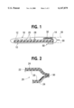
- FIG. 1 is a side elevational diagrammatic view in cross-section of an assembly of an electronic device in the form of a printed circuit board disposed within a flexible container and according to a first embodiment
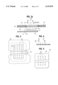
- FIG. 5 is a plan view in the direction of arrow V in FIG. 4;
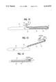
- FIG. 11 is a view similar to FIG. 6 of part of a modified method of assembly of the printed circuit board into the container of the first embodiment
- FIGS. 13 and 14 show stages in a method of assembly of a structure according to a fifth embodiment.
- an assembly 10 of a printed circuit board and flexible container comprises a printed circuit board 12 of conventional construction, the printed circuit board having an elongate electrical connector 14 connected along one edge region of the board in conventional manner.
- a flexible container 16 of the assembly is manufactured with an open end 18 (shown in chaindotted in FIG. 1) and into which the printed circuit board 12 and accompanying connector 14 has been inserted as a sub-assembly.
- the container 16 is of laminate construction wall and requires an EMI protection layer for the purpose of preventing or substantially diminishing the amount of magnetic radiation penetrating the container either to or from electronic components 20 mounted upon the printed circuit board.
- a thin metal layer 22 e.g.copper or other suitable conductive material
- the layer 22 may be of any desired thickness while being suitable for its desired purpose. It is found that a thickness down to 0.5 mil will suffice.
- the layer 22 is also imperforate and thus also serves as a moisture or other fluid barrier through the wall of the container.
- the layer 22 is perforate while still satisfying its EMI protection requirements and a specific moisture impermeable layer (not shown) is then included in the container.
- This specific layer may, for instance, be made from polyvinylidene chloride (such as sold under the Trademark "Saran”).
- An outer layer 24 is required to provide strength to the container and also to have abrasion and cutting resistance. In addition, it should also have dielectric properties. Any suitable polymeric material may do for this purpose, e.g polyethyleneterephthalate, possibly sold under the trade name "Mylar". Other materials are also suitable including polypropylene or polyamide.
- the outer layer is of a desired thickness to provide required flexibility. A thickness of at least 1 mil is found suitable.
- An inner layer 26 which faces inwardly into a chamber 28 (FIG. 1) within the container needs also to be of dielectric material (basically to prevent shorting of circuitry on the printed circuit board should the container contact any surface of the board or contact any electrical conductor carried by the board). With the particular requirements of the container, it is also necessary for the material of the inner layer to be such that it will fuse and heatseal to itself.
- a suitable material, and as used in this embodiment, is polyethylene.
- marginal edge regions 30 of the container 16 at the opening 18 have been brought together with inside surfaces provided by the polyethylene inner layer 26 abutted and then heatsealed together. An airtight seal along the fused together marginal edge regions 30 is thus provided airtightly sealing the chamber 28 within the container from the outside environment.
- the printed circuit board 12 communicates electrically with equipment exteriorly of the container 16 by means of a plurality of individually insulated conductors which extend from terminals of the connector 14 to present ends facing outwardly from the container for connection to the electrical equipment exteriorly of the container.
- these individually insulated conductors comprise a plurality of individually insulated conductor wires 32 (see FIGS. 1 and 2a) which extend from the terminals of the connector 14 and are soldered to electrically conductive elements 34 which are carried by the wall of the container as will now be described.
- the wall of the container is a laminate construction wall comprising the three layers 22, 24 and 26. However, in this embodiment the laminate construction wall is formed with an elongate aperture 36 (see FIG.
- the carrier 38 is a single layer of a dielectric material, e.g. polyethylene, polypropylene or polyamide for instance, which may be bonded or heat sealed to either or both of the inner and outer layers 24 and 26 of the laminate construction wall.
- a dielectric material e.g. polyethylene, polypropylene or polyamide for instance
- the dielectric material of the carrier 38 holds the electrically conductive elements 34 spaced apart and electrically isolated from each other and conveniently these elements are relatively positioned in a pattern which corresponds to the pattern of the terminals in the connector 14 from which the conductor wires 32 extend.
- each of the elements 34 has an end facing inwardly into the container 16 which is connected to a corresponding conductor wire 32, and another end which faces outwardly from the container and is exposed for soldering to another insulated conductor wire, e.g. as shown as item 33 FIG. 2a, and which extends to other electrical equipment or to an electrical power source.
- the aperture 36 as shown by FIG. 2a, has marginal regions provided by aperture defining dielectric projections 44 of the layers 24, 26 which project outwardly beyond the EMI protection layer.
- the carrier 38 is inserted between the projections 44 and is bonded or heat sealed thereto as required to seal across the aperture.
- the boundary of the carrier 38 is shown in FIG. 3 which indicates that all the marginal regions of the carrier lie between the projections 44.
- the method of making such an assembly including manufacture of the container itself may be quite economical and simple as will now be described. Firstly in the manufacture of the container, because the electrically conductive elements 34 are mounted in a separate carrier 38, then these elements need only be relatively positioned within the carrier without their relationship being determined initially to the laminate construction wall. The assembly of the elements 34 and the carrier 38 are simple compared to an alternative assembly of, and positioning of the elements 34, directly into the laminate construction wall itself.
- the assembly of the printed circuit board into the container is also simple and economical.
- the printed circuit board 12 is initially positioned outside the container 16 with the connector 14 mounted upon the board.
- the individually insulated conductor wires 32 are connected to terminals of the connector 14 and have their other ends pre-soldered to the electrically conductive elements 34 before the assembly of board and connector is mounted in position within the container wall.
- FIG. 6 shows the board 10 and connector 14 exteriorly of the container with the conductors 32 extending through the open end 18 and through the aperture 36 to be soldered to the elements 34.
- the assembly 40 is then inserted in position into the laminate construction wall as shown in FIG. 2a and is sealed therein.
- FIGS. 7 and 8 show firstly the assembly 40 located and sealed in position and then the closed end 30 being formed. It should be stressed, however, that the assembly steps after the wires 32 have been soldered to the conductive elements 34 may be easily changed while providing the same result.
- the printed circuit board and connector 14 may be positioned within the chamber 28 before the assembly 40 is located into position and sealed therein and the aperture 36 may be closed and sealed either before or after the closing and sealing of the open end 18 of the container.
- the carrier 38 is bonded to the outside surface of the container 16, i.e. the outside surface of the layer 24, and the aperture 36 may be of the same size and dimensions right through the laminate construction wall without the projections 44 being provided.
- a carrier 50 comprises an EMI protection layer 52 which may be of the same material as the layer 22 and of similar thickness.
- a dielectric layer 54 of any suitable polymeric material.
- Each layer 54 is of suitable size and shape to fit within the aperture 36.
- An outer layer 56 which projects outwardly beyond the layer 54 in all directions, overlaps the marginal regions of the aperture provided by layer 24 and is bonded to the layer 24.
- the layer 56 may be of the same material as the layer 24.
- An inner layer 58 of similar dimensions to the layer 56 overlaps the inner layer 26.
- the layer 58 is conveniently of the same material as the layer 26 and is heat sealed thereto.
- the EMI protection layer 52 will prevent EMI radiation through the area provided by the aperture 36 with the assembly 50 in position in the finished assembly.
- the EMI protection layer 52 has clearance holes 53 to space it from the conductive elements 34 and dielectric polymeric material lying within the clearance holes electrically isolates the elements 34 from the layer 92.
- individually insulated conductors extending from the connector 14 include a wire portion 32 and electrically conductive elements 34 mounted in a carrier. This is by no means an essential construction of the invention as will now be shown by the fourth embodiment.
- the printed circuit 12 and connector 14 are provided as in previous embodiments.
- the conductors which extend from terminals of the connector 14 and through a carrier 60 are composed entirely of individually electrically insulated conductor wires 62. These wires 62 pass through the carrier 60 which is molded around the wires so that end regions 64 of the conductor wires project exteriorly of the container in the finished assembly for connection to other electrical equipment.
- the carrier 60 may be of basically the same construction as the carrier 50 of the third embodiment, but in the fourth embodiment, the EMI protection layer is separated from each of the conductor wires 62 by the insulation layer 68 on each of the wires.
- the finished assembly of the carrier 60, conductor wires 62 and printed circuit board 12 with its connector 14 is then passed through the open end 18 of the container 16.
- the wires 62 are passed through the aperture 36 to position the carrier 60 outside the container as shown in FIG. 12.
- the open end 18 is then closed to provide the closed end 30,not shown in FIG. 12, and the carrier 60 is moved in the direction of the arrow in FIG. 12 to mount it in the position of the carrier 50 in the third embodiment to be sealed to close the opening 36.
- the carrier for the conductors or the electrically conductive elements as the case may be, should be placed upon and sealed across an aperture which is separate from the opening to the container and through which the printed circuit board 12 is inserted.
- a single opening 70 is provided towards one end of the container 72.
- the opening is sufficiently large to enable the printed circuit board 12 to be passed through it together with its connector 14 as shown by the arrow in FIG. 13.
- the carrier which may be of any construction including the constructions described in the above embodiments, is placed upon or within the opening 70 to be sealed in position so as to close the chamber from ambient atmosphere.
Abstract
Description
Claims (24)
Priority Applications (1)
| Application Number | Priority Date | Filing Date | Title |
|---|---|---|---|
| US08/989,719 US6147879A (en) | 1997-12-12 | 1997-12-12 | Assemblies of electrical devices and flexible containers therefor |
Applications Claiming Priority (1)
| Application Number | Priority Date | Filing Date | Title |
|---|---|---|---|
| US08/989,719 US6147879A (en) | 1997-12-12 | 1997-12-12 | Assemblies of electrical devices and flexible containers therefor |
Publications (1)
| Publication Number | Publication Date |
|---|---|
| US6147879A true US6147879A (en) | 2000-11-14 |
Family
ID=25535404
Family Applications (1)
| Application Number | Title | Priority Date | Filing Date |
|---|---|---|---|
| US08/989,719 Expired - Fee Related US6147879A (en) | 1997-12-12 | 1997-12-12 | Assemblies of electrical devices and flexible containers therefor |
Country Status (1)
| Country | Link |
|---|---|
| US (1) | US6147879A (en) |
Cited By (6)
| Publication number | Priority date | Publication date | Assignee | Title |
|---|---|---|---|---|
| US20020071940A1 (en) * | 2000-09-18 | 2002-06-13 | Shielding For Electronics, Inc. | Multi-layered structures and methods for manufacturing the multi-layered structures |
| US20040048077A1 (en) * | 1994-06-06 | 2004-03-11 | Shielding For Electronis, Inc. | Electromagnetic interference shield for electronic devices |
| DE10247676A1 (en) * | 2002-10-12 | 2004-07-15 | Hella Kg Hueck & Co. | Electronic circuit boards used in such as road vehicle equipment is protected by all over cover of plastic foil |
| US20040198078A1 (en) * | 2003-04-02 | 2004-10-07 | Canon Kabushiki Kaisha | Electronic apparatus |
| US9002288B1 (en) * | 2012-01-25 | 2015-04-07 | James Patrick Reible | Configurable shielded enclosure with signal transfer element |
| US10595451B1 (en) * | 2018-12-05 | 2020-03-17 | Getac Technology Corporation | Shielding structure of circuit board and electronic device having the same |
Citations (4)
| Publication number | Priority date | Publication date | Assignee | Title |
|---|---|---|---|---|
| US5436803A (en) * | 1993-12-16 | 1995-07-25 | Schlegel Corporation | Emi shielding having flexible conductive envelope |
| US5527989A (en) * | 1993-02-11 | 1996-06-18 | Telefonaktiebolaget Lm Ericsson | Flexible device for encapsulating electronic components |
| US5545494A (en) * | 1995-08-10 | 1996-08-13 | Northern Telecom Limited | Environmental protectors for electronics devices |
| US5739463A (en) * | 1994-04-11 | 1998-04-14 | Raychem Corporation | Sealed electronic packaging for environmental protection of active electronics |
-
1997
- 1997-12-12 US US08/989,719 patent/US6147879A/en not_active Expired - Fee Related
Patent Citations (4)
| Publication number | Priority date | Publication date | Assignee | Title |
|---|---|---|---|---|
| US5527989A (en) * | 1993-02-11 | 1996-06-18 | Telefonaktiebolaget Lm Ericsson | Flexible device for encapsulating electronic components |
| US5436803A (en) * | 1993-12-16 | 1995-07-25 | Schlegel Corporation | Emi shielding having flexible conductive envelope |
| US5739463A (en) * | 1994-04-11 | 1998-04-14 | Raychem Corporation | Sealed electronic packaging for environmental protection of active electronics |
| US5545494A (en) * | 1995-08-10 | 1996-08-13 | Northern Telecom Limited | Environmental protectors for electronics devices |
Cited By (10)
| Publication number | Priority date | Publication date | Assignee | Title |
|---|---|---|---|---|
| US20040048077A1 (en) * | 1994-06-06 | 2004-03-11 | Shielding For Electronis, Inc. | Electromagnetic interference shield for electronic devices |
| US20070199738A1 (en) * | 1994-06-06 | 2007-08-30 | Wavezero, Inc. | Electromagnetic Interference Shields for Electronic Devices |
| US7358447B2 (en) | 1994-06-06 | 2008-04-15 | Wavezero, Inc. | Electromagnetic interference shields for electronic devices |
| US20020071940A1 (en) * | 2000-09-18 | 2002-06-13 | Shielding For Electronics, Inc. | Multi-layered structures and methods for manufacturing the multi-layered structures |
| US6768654B2 (en) * | 2000-09-18 | 2004-07-27 | Wavezero, Inc. | Multi-layered structures and methods for manufacturing the multi-layered structures |
| DE10247676A1 (en) * | 2002-10-12 | 2004-07-15 | Hella Kg Hueck & Co. | Electronic circuit boards used in such as road vehicle equipment is protected by all over cover of plastic foil |
| US20040198078A1 (en) * | 2003-04-02 | 2004-10-07 | Canon Kabushiki Kaisha | Electronic apparatus |
| US6870094B2 (en) * | 2003-04-02 | 2005-03-22 | Canon Kabushiki Kaisha | Electronic apparatus |
| US9002288B1 (en) * | 2012-01-25 | 2015-04-07 | James Patrick Reible | Configurable shielded enclosure with signal transfer element |
| US10595451B1 (en) * | 2018-12-05 | 2020-03-17 | Getac Technology Corporation | Shielding structure of circuit board and electronic device having the same |
Similar Documents
| Publication | Publication Date | Title |
|---|---|---|
| US5452948A (en) | Apparatus and method for electronically controlled hydraulic actuator | |
| US6219258B1 (en) | Electronic enclosure with improved environmental protection | |
| JP3879936B2 (en) | Shield housing and shield housing manufacturing method | |
| US5392197A (en) | Moisture proof of electric device for motor vehicles | |
| CN102231946B (en) | Field device incorporating circuit card assembly as environmental and EMI/RFI shield | |
| JP3009634B2 (en) | Electronic assembly with environmental protection or electromagnetic interference shielding | |
| US5266054A (en) | Sealed and filtered header receptacle | |
| KR101809288B1 (en) | Method for integrating an electronic component into a printed circuit board, and printed circuit board comprising an electronic component integrated therein | |
| JP2894325B2 (en) | Electronic circuit shield structure | |
| US5527989A (en) | Flexible device for encapsulating electronic components | |
| US7085142B2 (en) | Electrical device | |
| US7813145B2 (en) | Circuit structure with multifunction circuit cover | |
| US6839214B2 (en) | Overvoltage protection device | |
| KR960000450A (en) | How to mold an electrical element in an integral housing | |
| US6028775A (en) | Assemblies of electronic devices and flexible containers thereof | |
| US6097613A (en) | Assemblies of electronic devices and flexible containers therefor | |
| US6147879A (en) | Assemblies of electrical devices and flexible containers therefor | |
| EP0504319B1 (en) | Lightweight sealed circuit board assembly | |
| US6094361A (en) | Assemblies of printed circuit boards and flexible containers therefor | |
| KR100272910B1 (en) | Pressure compensation element and terminal strip | |
| US5438160A (en) | Sealed, shielded and filtered header receptacle | |
| US8674220B2 (en) | Electronics housing with standard interface | |
| US6035513A (en) | Assemblies of electronic devices and flexible containers therefor | |
| US5981103A (en) | Assemblies of electronic devices and flexible containers therefor | |
| JP2000058692A (en) | Package for electronic components |
Legal Events
| Date | Code | Title | Description |
|---|---|---|---|
| AS | Assignment |
Owner name: NORTHERN TELECOM LIMITED, CANADA Free format text: ASSIGNMENT OF ASSIGNORS INTEREST;ASSIGNORS:BATTEN, L. EUGENE JR.;MCCULLOCH, DENNIS A.;FORDHAM, MARK J.;REEL/FRAME:008910/0080 Effective date: 19971209 |
|
| AS | Assignment |
Owner name: NORTEL NETWORKS CORPORATION, CANADA Free format text: CHANGE OF NAME;ASSIGNOR:NORTHERN TELECOM LIMITED;REEL/FRAME:010567/0001 Effective date: 19990429 |
|
| AS | Assignment |
Owner name: NORTEL NETWORKS LIMITED, CANADA Free format text: CHANGE OF NAME;ASSIGNOR:NORTEL NETWORKS CORPORATION;REEL/FRAME:011195/0706 Effective date: 20000830 Owner name: NORTEL NETWORKS LIMITED,CANADA Free format text: CHANGE OF NAME;ASSIGNOR:NORTEL NETWORKS CORPORATION;REEL/FRAME:011195/0706 Effective date: 20000830 |
|
| FEPP | Fee payment procedure |
Free format text: PAYOR NUMBER ASSIGNED (ORIGINAL EVENT CODE: ASPN); ENTITY STATUS OF PATENT OWNER: LARGE ENTITY |
|
| FPAY | Fee payment |
Year of fee payment: 4 |
|
| REMI | Maintenance fee reminder mailed | ||
| LAPS | Lapse for failure to pay maintenance fees | ||
| STCH | Information on status: patent discontinuation |
Free format text: PATENT EXPIRED DUE TO NONPAYMENT OF MAINTENANCE FEES UNDER 37 CFR 1.362 |
|
| FP | Lapsed due to failure to pay maintenance fee |
Effective date: 20081114 |