US6150683A - CMOS-based color pixel with reduced noise in the blue signal - Google Patents
CMOS-based color pixel with reduced noise in the blue signal Download PDFInfo
- Publication number
- US6150683A US6150683A US08/883,677 US88367797A US6150683A US 6150683 A US6150683 A US 6150683A US 88367797 A US88367797 A US 88367797A US 6150683 A US6150683 A US 6150683A
- Authority
- US
- United States
- Prior art keywords
- region
- doping concentration
- forming
- conductivity type
- substrate
- Prior art date
- Legal status (The legal status is an assumption and is not a legal conclusion. Google has not performed a legal analysis and makes no representation as to the accuracy of the status listed.)
- Expired - Lifetime
Links
- 239000000758 substrate Substances 0.000 claims description 42
- 238000000034 method Methods 0.000 claims description 18
- 238000003384 imaging method Methods 0.000 abstract description 8
- 238000010586 diagram Methods 0.000 description 15
- 238000005215 recombination Methods 0.000 description 11
- 230000006798 recombination Effects 0.000 description 11
- 230000003321 amplification Effects 0.000 description 9
- 238000003199 nucleic acid amplification method Methods 0.000 description 9
- 239000000969 carrier Substances 0.000 description 6
- 230000010354 integration Effects 0.000 description 6
- 238000006243 chemical reaction Methods 0.000 description 5
- 230000035515 penetration Effects 0.000 description 5
- 230000005684 electric field Effects 0.000 description 4
- 238000004519 manufacturing process Methods 0.000 description 2
- 230000009467 reduction Effects 0.000 description 2
- 101100041125 Arabidopsis thaliana RST1 gene Proteins 0.000 description 1
- 101100443250 Saccharomyces cerevisiae (strain ATCC 204508 / S288c) DIG1 gene Proteins 0.000 description 1
- 230000015572 biosynthetic process Effects 0.000 description 1
- 230000035945 sensitivity Effects 0.000 description 1
Images
Classifications
-
- H—ELECTRICITY
- H01—ELECTRIC ELEMENTS
- H01L—SEMICONDUCTOR DEVICES NOT COVERED BY CLASS H10
- H01L27/00—Devices consisting of a plurality of semiconductor or other solid-state components formed in or on a common substrate
- H01L27/14—Devices consisting of a plurality of semiconductor or other solid-state components formed in or on a common substrate including semiconductor components sensitive to infrared radiation, light, electromagnetic radiation of shorter wavelength or corpuscular radiation and specially adapted either for the conversion of the energy of such radiation into electrical energy or for the control of electrical energy by such radiation
- H01L27/144—Devices controlled by radiation
- H01L27/146—Imager structures
- H01L27/14643—Photodiode arrays; MOS imagers
- H01L27/14645—Colour imagers
-
- H—ELECTRICITY
- H01—ELECTRIC ELEMENTS
- H01L—SEMICONDUCTOR DEVICES NOT COVERED BY CLASS H10
- H01L31/00—Semiconductor devices sensitive to infrared radiation, light, electromagnetic radiation of shorter wavelength or corpuscular radiation and specially adapted either for the conversion of the energy of such radiation into electrical energy or for the control of electrical energy by such radiation; Processes or apparatus specially adapted for the manufacture or treatment thereof or of parts thereof; Details thereof
- H01L31/0248—Semiconductor devices sensitive to infrared radiation, light, electromagnetic radiation of shorter wavelength or corpuscular radiation and specially adapted either for the conversion of the energy of such radiation into electrical energy or for the control of electrical energy by such radiation; Processes or apparatus specially adapted for the manufacture or treatment thereof or of parts thereof; Details thereof characterised by their semiconductor bodies
- H01L31/0352—Semiconductor devices sensitive to infrared radiation, light, electromagnetic radiation of shorter wavelength or corpuscular radiation and specially adapted either for the conversion of the energy of such radiation into electrical energy or for the control of electrical energy by such radiation; Processes or apparatus specially adapted for the manufacture or treatment thereof or of parts thereof; Details thereof characterised by their semiconductor bodies characterised by their shape or by the shapes, relative sizes or disposition of the semiconductor regions
- H01L31/035272—Semiconductor devices sensitive to infrared radiation, light, electromagnetic radiation of shorter wavelength or corpuscular radiation and specially adapted either for the conversion of the energy of such radiation into electrical energy or for the control of electrical energy by such radiation; Processes or apparatus specially adapted for the manufacture or treatment thereof or of parts thereof; Details thereof characterised by their semiconductor bodies characterised by their shape or by the shapes, relative sizes or disposition of the semiconductor regions characterised by at least one potential jump barrier or surface barrier
- H01L31/03529—Shape of the potential jump barrier or surface barrier
-
- H—ELECTRICITY
- H01—ELECTRIC ELEMENTS
- H01L—SEMICONDUCTOR DEVICES NOT COVERED BY CLASS H10
- H01L31/00—Semiconductor devices sensitive to infrared radiation, light, electromagnetic radiation of shorter wavelength or corpuscular radiation and specially adapted either for the conversion of the energy of such radiation into electrical energy or for the control of electrical energy by such radiation; Processes or apparatus specially adapted for the manufacture or treatment thereof or of parts thereof; Details thereof
- H01L31/08—Semiconductor devices sensitive to infrared radiation, light, electromagnetic radiation of shorter wavelength or corpuscular radiation and specially adapted either for the conversion of the energy of such radiation into electrical energy or for the control of electrical energy by such radiation; Processes or apparatus specially adapted for the manufacture or treatment thereof or of parts thereof; Details thereof in which radiation controls flow of current through the device, e.g. photoresistors
- H01L31/10—Semiconductor devices sensitive to infrared radiation, light, electromagnetic radiation of shorter wavelength or corpuscular radiation and specially adapted either for the conversion of the energy of such radiation into electrical energy or for the control of electrical energy by such radiation; Processes or apparatus specially adapted for the manufacture or treatment thereof or of parts thereof; Details thereof in which radiation controls flow of current through the device, e.g. photoresistors characterised by at least one potential-jump barrier or surface barrier, e.g. phototransistors
- H01L31/101—Devices sensitive to infrared, visible or ultraviolet radiation
- H01L31/102—Devices sensitive to infrared, visible or ultraviolet radiation characterised by only one potential barrier or surface barrier
- H01L31/103—Devices sensitive to infrared, visible or ultraviolet radiation characterised by only one potential barrier or surface barrier the potential barrier being of the PN homojunction type
-
- Y—GENERAL TAGGING OF NEW TECHNOLOGICAL DEVELOPMENTS; GENERAL TAGGING OF CROSS-SECTIONAL TECHNOLOGIES SPANNING OVER SEVERAL SECTIONS OF THE IPC; TECHNICAL SUBJECTS COVERED BY FORMER USPC CROSS-REFERENCE ART COLLECTIONS [XRACs] AND DIGESTS
- Y02—TECHNOLOGIES OR APPLICATIONS FOR MITIGATION OR ADAPTATION AGAINST CLIMATE CHANGE
- Y02E—REDUCTION OF GREENHOUSE GAS [GHG] EMISSIONS, RELATED TO ENERGY GENERATION, TRANSMISSION OR DISTRIBUTION
- Y02E10/00—Energy generation through renewable energy sources
- Y02E10/50—Photovoltaic [PV] energy
Definitions
- the present invention relates to CMOS-based color pixels and, more particularly, to a CMOS-based color pixel with reduced noise in the blue signal.
- CCDs Charge-coupled devices
- CCDs have been the mainstay of conventional imaging circuits for converting a pixel of light energy into an electrical signal that represents the intensity of the light energy.
- CCDs utilize a photogate to convert the light energy into an electrical charge, and a series of electrodes to transfer the charge collected at the photogate to an output sense node.
- CCDs have many strengths, which include a high sensitivity and fill-factor, CCDs also suffer from a number of weaknesses. Most notable among these weaknesses, which include limited readout rates and dynamic range limitations, is the difficulty in integrating CCDs with CMOS-based microprocessors.
- active pixel sensor cells To overcome the limitations of CCD-based imaging circuits, more recent imaging circuits use active pixel sensor cells to convert a pixel of light energy into an electrical signal.
- active pixel sensor cells With active pixel sensor cells, a conventional photodiode is combined with a number of active transistors which, in addition to forming an electrical signal, provide amplification, readout control, and reset control.
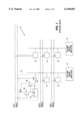
- FIG. 1 shows a cross-sectional and schematic diagram that illustrates a portion of a conventional CMOS active pixel sensor cell array 10.
- array 10 includes a plurality of active pixel sensor cells 12 which are formed in rows and columns, and a plurality of column sense amplifiers 14 which are connected to the cells 12 so that one amplifier 14 is connected to each cell 12 in a column of cells.
- each cell 12 which is formed in a lightly-doped, e.g., 1 ⁇ 10 14 to 1 ⁇ 10 15 atoms/cm 3 , p-type substrate 16 (or an epitaxial (epi) layer), includes a heavily-doped, e.g., 5 ⁇ 10 15 to 1 ⁇ 10 19 atoms/cm 3 , n+ region 18 which is formed in substrate 16 (or the epi layer) to function as a photodiode, and a reset transistor 20 which has a source connected to n+ region 18 and a gate connected to receive one of a plurality of reset signals RST1-RSTn.
- a lightly-doped e.g., 1 ⁇ 10 14 to 1 ⁇ 10 15 atoms/cm 3
- p-type substrate 16 or an epitaxial (epi) layer
- n+ region 18 which is formed in substrate 16 (or the epi layer) to function as a photodiode
- reset transistor 20 which has a source connected to n
- each cell 12 also includes a source-follower transistor 22 which has a gate connected to n+ region 18, and a row-select transistor 24 which has a drain connected to the source of source-follower transistor 22 and a gate connected to receive one of a plurality of row-select signals RWSL1-RWSLn.
- array 10 first sequentially resets each row of cells in the array.
- the potential on n+ region 18 of each cell 12 in the first row of cells is raised to an initial transfer voltage by pulsing the gates of the reset transistors 20 in the first row with a positive voltage via the reset signal RST1.
- the initial transfer voltage placed on n+ region 18 of each cell in turn, defines an initial intermediate voltage on the source of each of the source-follower transistors 22 in the first row.
- the gates of the row-select transistors 24 in the first row are pulsed with a positive voltage via the row-select signal RWSL1.
- the positive voltage on the gates of the row-select transistors 24 causes the initial intermediate voltages on the sources of the source-follower transistors 22 to appear on the sources of the row-select transistors 24 as initial integration voltages.
- the initial integration voltage of each cell 12 in the first row is sensed and amplified by the column sense amplifier 14 that corresponds with each cell 12 in the row, and then stored by an imaging system (not shown). The same process is then repeated on the remaining rows in the array.
- the photogenerated electrons formed in substrate 16 (or the epi layer) of the cell 12 which diffuse over to the junction region are attracted to n+ region 18 of the cell 12 under the influence of the junction electric field, while the photogenerated electrons formed in n+ region 18 of the cell 12 remain in n+ region 18 where each additional electron reduces the potential on n+ region 18 of the cell 12.
- the potential on n+ region 18 of each cell 12 in the first row will have been reduced to a final transfer voltage where the amount of the reduction represents the intensity of the received light energy.
- the final transfer voltage on n+ region 18 of each cell 12 in the first row is then read out via the source-follower transistors 22 of each cell 12 as a final integration voltage by again pulsing the gates of the row-select transistors 24 in the first row.
- the total charge collected by each cell 12 in the first row is determined by subtracting the final integration voltage of the cell from the initial integration voltage of the cell.
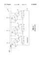
- FIG. 2 shows a cross-sectional and schematic diagram that illustrates a conventional color pixel 50.
- color pixel 50 which uses the same reference numerals to designate the structures which are common to both FIGS. 1 and 2, includes a red active pixel sensor cell 52, a green active pixel sensor cell 54, and a blue active pixel sensor cell 56.
- red cell 52 only differs from cells 12 of FIG. 1 in that red cell 52 includes a red filter 60 which only passes red photons.
- green and blue cells 54 and 56 only differ from cells 12 in that green and blue cells 54 and 56 include green and blue filters 62 and 64, respectively, which only pass green and blue photons.
- cells 52, 54, and 56 operate the same as cells 12 of FIG. 1 except that the information provided by red, green, and blue cells 52, 54, and 56 is limited to the intensities of the red, green, and blue lights, respectively.
- This difference in recombination rates is due to the relatively shallow penetration depths of the blue photons, the higher majority carrier concentration that exists in n+ region 18 than exists in substrate 16 (or the epi layer), and the depth of the junction.
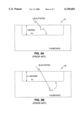
- FIG. 3A shows a cross-sectional diagram that illustrates a conventional n+/p- CCD photodiode 70
- FIG. 3B shows a conventional n+/p- CMOS photodiode 80
- the typical junction depth of a CCD photodiode is approximately one micron
- the typical junction depth of a CMOS photodiode based on a 0.25 micron photolithographic process is approximately 0.1 microns.
- blue photons typically penetrate about 0.2 microns into the photodiode before interacting with the lattice to form electron-hole pairs (EHPs).
- EHPs electron-hole pairs
- the average penetration depth of the blue photons means that the majority of the EHPs are formed in the n+ region, whereas with CMOS photodiodes the majority of blue EHPs are formed in the substrate.
- the photogenerated electrons formed in the n+ region remain in the n+ region, while the photogenerated holes formed in the n+ region diffuse over to the junction where the holes are swept into the substrate under the influence of the junction electric field.
- the high concentration of majority carriers in the n+ region a high percentage of the holes in the CCD photodiode are lost to recombination in the n+ region before being collected by the substrate.
- the photogenerated holes formed in the substrate remain in the substrate, while the photogenerated electrons formed in the substrate diffuse over to the junction where the electrons are swept into the n+ region under the influence of the junction electric field.
- CMOS photodiodes provide a substantially better blue response than CCD photodiodes.
- CMOS photodiodes provide a substantially better blue response than CCD photodiodes, the blue response of a CMOS photodiode remains substantially below the red and green responses of a CMOS photodiode.
- the poor blue response of CMOS photodiodes exists because, even though the average penetration depth of a blue photon is approximately 0.2 microns, a large number of the blue photons fail to penetrate beyond the 0.1 micron junction. As a result, a large number of these photons are still lost to recombination.
- the average penetration depth of red and green photons is on the order of several microns. At this depth, the EHPs formed from the red and green photons are almost exclusively formed in the substrate rather than the n+ region.
- One technique for equalizing the red, green, and blue responses is to increase the amplification provided by the column sense amplifiers 14 that correspond with the blue cells 56. For example, if the blue response is 10 ⁇ lower than the red and green responses, equalized red, green, and blue responses are obtained if the column sense amplifiers 14 that correspond with the red and green cells 52 and 54 are set to provide unity gain, and the column sense amplifiers 14 that correspond with the blue cells 56 are set to provide a gain of 10 ⁇ .
- CMOS-based color pixels suffer from a blue signal that is substantially noisier than the red and green signals.
- the increased noise results from the substantial amplification of the blue signal which is required to balance the much smaller blue signal with the larger red and green signals.
- the substantial amplification of the blue signal in turn, also amplifies the noise associated with the blue signal.
- the small blue signal results from the inability of blue photons to penetrate beyond the heavily-doped surface region of a pn-junction photodiode. As a result of this shallow penetration, the minority carriers that are formed from the blue photons experience a significantly higher recombination rate than the minority carriers formed from red and green photons.
- the present invention increases the magnitude of the blue response by lowering the doping concentration of the surface region of the pn-junction photodiode used to collect blue photons with respect to the surface regions of the pn-junction photodiodes that are used to collect red and green photons.
- the charge representing the blue photons is increased prior to the noisy step of converting the charge into a voltage. Even modest increases in the charge at this stage can significantly reduce the noise associated with the amplified blue signal.
- a color pixel in accordance with the present invention which is formed in a substrate of a first conductivity type, includes first, second, and third regions of a second conductivity type which are each formed in the substrate.
- the doping concentrations of the first and second regions are substantially equal.
- the doping concentration of the third region is substantially less than the doping concentration of the first region.
- the color pixel also includes first, second, and third reset transistors which each have a source where the source of the first reset transistor is connected to the first region, the source of the second transistor is connected to the second region, and the source of the third transistor is connected to the third region.
- FIG. 1 is a cross-sectional and schematic diagram illustrating a portion of a conventional CMOS active pixel sensor cell array 10.
- FIG. 2 is a cross-sectional and schematic diagram illustrating a conventional color pixel 50.
- FIG. 3A is a cross-sectional diagram illustrating a conventional n+/p- CCD photodiode 70.
- FIG. 3B is a cross-sectional diagram illustrating a conventional n+/p- CMOS photodiode 80.
- FIG. 4 is a cross-sectional and schematic diagram illustrating a color pixel 100 in accordance with the present invention.
- FIG. 5 is a cross-sectional and schematic diagram illustrating a color pixel 200 in accordance with a first alternate embodiment of the present invention.
- FIG. 6 is a cross-sectional and schematic diagram illustrating a color pixel 300 in accordance with a second alternate embodiment of the present invention.
- FIG. 7 is a cross-sectional and schematic diagram illustrating a color pixel 400 in accordance with a third alternate embodiment of the present invention.
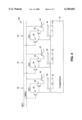
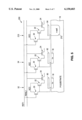
- FIG. 4 shows a cross-sectional and schematic diagram that illustrates a color pixel 100 in accordance with the present invention.
- color pixel 100 increases the blue response with respect to the red and green responses by lowering the doping concentration of the n-type regions used to form the photodiodes of the blue cells with respect to the n-type regions used to form the photodiodes of the red and green cells.
- pixel 100 which uses the same reference numerals to designate the structures which are common to both FIGS. 2 and 4, includes a red active pixel sensor cell 52, a green active pixel sensor cell 54, and a blue active pixel sensor cell 110.
- blue cell 110 of FIG. 4 differs from blue cell 56 of FIG. 2 in that blue cell 110 utilizes a moderately-doped, e.g., approximately 5 ⁇ 10 14 to 1 ⁇ 10 17 atoms/cm 3 , n-type region 112 to form a photodiode in lightly-doped, e.g., 1 ⁇ 10 14 to 1 ⁇ 10 15 atoms/cm 3 , substrate 16 (or the epi layer) in lieu of the heavily-doped, e.g., approximately 5 ⁇ 10 15 to 1 ⁇ 10 19 atoms/cm 3 , n+ region 18 utilized by blue cell 56.
- a moderately-doped e.g., approximately 5 ⁇ 10 14 to 1 ⁇ 10 17 atoms/cm 3
- n-type region 112 to form a photodiode in lightly-doped, e.g., 1 ⁇ 10 14 to 1 ⁇ 10 15 atoms/cm 3 , substrate 16 (or the epi layer) in lieu of the heavily
- cells 52 and 54 of FIG. 4 operate the same as cells 52 and 54 of FIG. 2.
- Cell 110 operates differently from cell 56 in that by utilizing a lower doping concentration in region 112 than is used in region 18, fewer holes are lost to recombination in region 112 of cell 110 than are lost in region 18 of cell 56 since fewer majority carriers are present in region 112 to participate in recombination. Since fewer holes are lost to recombination, region 112 is able to collect more electrons than region 18.
- the junction capacitance of cell 110 is less than the junction capacitance of cell 56.
- cell 110 collects more photogenerated electrons than cell 56, and provides a higher charge-to-voltage conversion ratio than cell 56.
- the voltage sensed from moderately-doped n-type region 112 of cell 110 will be greater than the voltage sensed from n+ region 18 of cell 56.
- pixel 100 of the present invention reduces the differences between the red, green, and blue responses before the noisy charge-to-voltage conversion stage. As a result, less amplification is needed by the column sense amplifiers to balance the red, green, and blue responses which, in turn, reduces the amplification of the noise associated with the blue signal.
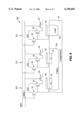
- FIG. 5 shows a cross-sectional and schematic diagram that illustrates a color pixel 200 in accordance with a first alternate embodiment of the present invention.
- pixel 200 which uses the same reference numerals to designate the structures which are common to both FIGS. 4 and 5, includes a red active pixel sensor cell 52, a green active pixel sensor cell 54, and a blue active pixel sensor cell 210.
- blue cell 210 of FIG. 5 differs from blue cell 110 of FIG. 4 in that blue cell 210 utilizes an n-well 212, which may be formed as a diffused or retrograde well, in lieu of n-type region 112.
- pixel 200 operates the same as pixel 100 except that n-well 212, which has approximately the same doping concentration as n-type region 112, has a slightly higher recombination rate than n-type region 112 due to the greater depth of n-well 212 than n-type region 112.
- pixel 200 reduces the noise associated with the blue response without increasing the time, cost, or complexity of the fabrication process.
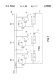
- FIG. 6 shows a cross-sectional and schematic diagram that illustrates a color pixel 300 in accordance with a second alternate embodiment of the present invention.
- pixel 300 which uses the same reference numerals to designate the structures which are common to both FIGS. 5 and 6, includes a red active pixel sensor cell 310, a green active pixel sensor cell 320, and a blue active pixel sensor cell 210.
- red and green cells 310 and 312 of FIG. 6 differ from red and green cells 52 and 54 of FIG. 5 in that n+ region 18 of red and green cells 310 and 312 are formed in a p-well 314 having a doping concentration in the range of 5 ⁇ 10 14 to 1 ⁇ 10 17 atoms/cm 3 which, in turn, is formed in substrate 16 (or the epi layer).
- pixel 300 operates the same as pixel 200 except that the red and green responses are slightly lower due to the increased junction capacitance that exists between n+ region 18 and p-well 314 of cell 300 as compared to the junction capacitance that exists between n+ region 18 and p-substrate 16 (or the epi layer).
- FIG. 7 shows a cross-sectional and schematic diagram that illustrates a color pixel 400 in accordance with a third alternate embodiment of the present invention.
- pixel 400 which uses the same reference numerals to designate the structures which are common to both FIGS. 6 and 7, includes a red active pixel sensor cell 310, a green active pixel sensor cell 320, and a blue active pixel sensor cell 410 which identical to blue cell 110 of FIG. 4.
- a color pixel has been described that increases the blue response of the pixel prior to the noisy charge-to-voltage conversion stage.
Abstract
Description
Claims (20)
Priority Applications (1)
| Application Number | Priority Date | Filing Date | Title |
|---|---|---|---|
| US08/883,677 US6150683A (en) | 1997-06-27 | 1997-06-27 | CMOS-based color pixel with reduced noise in the blue signal |
Applications Claiming Priority (1)
| Application Number | Priority Date | Filing Date | Title |
|---|---|---|---|
| US08/883,677 US6150683A (en) | 1997-06-27 | 1997-06-27 | CMOS-based color pixel with reduced noise in the blue signal |
Publications (1)
| Publication Number | Publication Date |
|---|---|
| US6150683A true US6150683A (en) | 2000-11-21 |
Family
ID=25383099
Family Applications (1)
| Application Number | Title | Priority Date | Filing Date |
|---|---|---|---|
| US08/883,677 Expired - Lifetime US6150683A (en) | 1997-06-27 | 1997-06-27 | CMOS-based color pixel with reduced noise in the blue signal |
Country Status (1)
| Country | Link |
|---|---|
| US (1) | US6150683A (en) |
Cited By (45)
| Publication number | Priority date | Publication date | Assignee | Title |
|---|---|---|---|---|
| US6310366B1 (en) * | 1999-06-16 | 2001-10-30 | Micron Technology, Inc. | Retrograde well structure for a CMOS imager |
| US6359323B1 (en) * | 1998-12-30 | 2002-03-19 | Hyundai Electronics Industries Co., Ltd. | Color image sensor and method for fabricating the same |
| US6365887B1 (en) * | 1997-08-12 | 2002-04-02 | Rohm Co., Ltd. | Image reading apparatus |
| US6445014B1 (en) * | 1999-06-16 | 2002-09-03 | Micron Technology Inc. | Retrograde well structure for a CMOS imager |
| US20020166951A1 (en) * | 2001-05-09 | 2002-11-14 | Yvon Cazaux | CMOS-type photodetector |
| US6504196B1 (en) * | 2001-08-30 | 2003-01-07 | Micron Technology, Inc. | CMOS imager and method of formation |
| US20030045020A1 (en) * | 2001-08-30 | 2003-03-06 | Rhodes Howard E. | COMS imager and method of formation |
| US6548833B1 (en) * | 2000-10-26 | 2003-04-15 | Biomorphic Vlsi, Inc. | Color-optimized pixel array design |
| US6583456B2 (en) * | 1998-09-16 | 2003-06-24 | Nec Corporation | Image sensor with light receiving elements of differing areas and image reader both having semiconductor device |
| US20030124753A1 (en) * | 2000-08-09 | 2003-07-03 | Taiwan Semiconductor Manufacturing Company | Method for making spectrally efficient photodiode structures for CMOS color imagers |
| US20030136982A1 (en) * | 2001-08-30 | 2003-07-24 | Rhodes Howard E. | CMOS imager and method of formation |
| US6606120B1 (en) * | 1998-04-24 | 2003-08-12 | Foveon, Inc. | Multiple storage node full color active pixel sensors |
| US6677656B2 (en) | 2001-02-12 | 2004-01-13 | Stmicroelectronics S.A. | High-capacitance photodiode |
| US20040043529A1 (en) * | 2002-08-29 | 2004-03-04 | Fossum Eric R. | Two-transistor pixel with buried reset channel and method of formation |
| US6704046B2 (en) * | 2002-04-17 | 2004-03-09 | Motorola, Inc. | Digital pixel image sensor with independent color channel reference signals |
| US20040104413A1 (en) * | 2002-11-26 | 2004-06-03 | Howard Rhodes | CMOS imager pixel designs |
| US6781169B2 (en) | 2001-02-12 | 2004-08-24 | Stmicroelectronics S.A. | Photodetector with three transistors |
| US20040201073A1 (en) * | 2003-04-14 | 2004-10-14 | Dialog Semiconductor Gmbh | Red/green pixel with simultaneous exposure and improved MTF |
| US6830951B2 (en) | 1998-07-28 | 2004-12-14 | Stmicroelectronics S.R.L. | Integrated semiconductor light sensor device and corresponding manufacturing process |
| US6844585B1 (en) | 2002-06-17 | 2005-01-18 | National Semiconductor Corporation | Circuit and method of forming the circuit having subsurface conductors |
| US6852562B1 (en) | 2003-12-05 | 2005-02-08 | Eastman Kodak Company | Low-cost method of forming a color imager |
| US6861673B1 (en) * | 1999-02-08 | 2005-03-01 | Intel Corporation | Chip CMOS optical element |
| US6870149B2 (en) | 1999-03-09 | 2005-03-22 | Micron Technology, Inc. | Superposed multi-junction color APS |
| US6881986B1 (en) * | 2001-11-07 | 2005-04-19 | Taiwan Semiconductor Manufacturing Company | Design and fabrication method for finger n-type doped photodiodes with high sensitivity for CIS products |
| US6924167B1 (en) | 2002-08-15 | 2005-08-02 | Foveon, Inc. | Method of forming a bandgap tuned vertical color imager cell |
| US6946715B2 (en) | 2003-02-19 | 2005-09-20 | Micron Technology, Inc. | CMOS image sensor and method of fabrication |
| US6958194B1 (en) | 2003-10-21 | 2005-10-25 | Foveon, Inc. | Imager with improved sensitivity |
| US6967121B2 (en) * | 1999-08-16 | 2005-11-22 | Micron Technology, Inc. | Buried channel CMOS imager and method of forming same |
| US6972457B1 (en) | 2004-04-09 | 2005-12-06 | Eastman Kodak Company | Imaging cell that has a long integration period and method of operating the imaging cell |
| US20060043519A1 (en) * | 2004-08-31 | 2006-03-02 | Sony Corporation | Solid-state imaging device, camera module and electronic equipment module |
| US7022968B1 (en) | 2003-10-21 | 2006-04-04 | National Semiconductor Corporation | Optical sensor that measures the light output by the combustion chamber of an internal combustion engine |
| US7105373B1 (en) | 2003-08-14 | 2006-09-12 | National Semiconductor Corporation | Vertical photodiode with heavily-doped regions of alternating conductivity types |
| US20060278943A1 (en) * | 2003-05-08 | 2006-12-14 | Turchetta Renato Andrea D | Accelerated particle and high energy radiation sensor |
| US20070045680A1 (en) * | 2005-08-30 | 2007-03-01 | Micron Technology, Inc. | Pixel cell arrays having pixel cells with color specific characteristics |
| US20070052825A1 (en) * | 2000-08-07 | 2007-03-08 | Kwang-Bo Cho | Pixel optimization for color |
| US7212240B1 (en) | 2001-05-25 | 2007-05-01 | Dalsa, Inc. | Imager with a row of photodiodes or pinned photo diodes |
| US20070257283A1 (en) * | 2006-05-03 | 2007-11-08 | Taiwan Semiconductor Manufacturing Company, Ltd. | Color filter-embedded MSM image sensor |
| US20070278604A1 (en) * | 2003-11-12 | 2007-12-06 | Rainer Minixhofer | Optoelectronic Component Which Can Detect Radiation |
| US20080129834A1 (en) * | 2006-11-28 | 2008-06-05 | Taner Dosluoglu | Simultaneous global shutter and correlated double sampling read out in multiple photosensor pixels |
| US20080198454A1 (en) * | 2007-02-19 | 2008-08-21 | Taiwan Semiconductor Manufacturing Company, Ltd. | Color Filter For Image Sensor |
| US20090014764A1 (en) * | 2007-07-12 | 2009-01-15 | Stmicroelectronics Sa | Image sensor with an improved sensitivity |
| US20090075838A1 (en) * | 2002-09-16 | 2009-03-19 | The Board Of Trustees Of The Leland Stanford Junior University | Biological Analysis Arrangement and Approach Therefor |
| US7602430B1 (en) * | 2007-04-18 | 2009-10-13 | Foveon, Inc. | High-gain multicolor pixel sensor with reset noise cancellation |
| US20170053958A1 (en) * | 2015-08-21 | 2017-02-23 | Samsung Electronics Co., Ltd. | Image sensor and electronic device including the same |
| TWI626333B (en) * | 2015-02-19 | 2018-06-11 | Tokyo Electron Ltd | Manufacturing method and memory medium for optical device including light shielding body |
Citations (4)
| Publication number | Priority date | Publication date | Assignee | Title |
|---|---|---|---|---|
| US5625210A (en) * | 1995-04-13 | 1997-04-29 | Eastman Kodak Company | Active pixel sensor integrated with a pinned photodiode |
| US5965875A (en) * | 1998-04-24 | 1999-10-12 | Foveon, Inc. | Color separation in an active pixel cell imaging array using a triple-well structure |
| US5969337A (en) * | 1997-04-29 | 1999-10-19 | Lucent Technologies Inc. | Integrated photosensing device for active pixel sensor imagers |
| US6021172A (en) * | 1994-01-28 | 2000-02-01 | California Institute Of Technology | Active pixel sensor having intra-pixel charge transfer with analog-to-digital converter |
-
1997
- 1997-06-27 US US08/883,677 patent/US6150683A/en not_active Expired - Lifetime
Patent Citations (4)
| Publication number | Priority date | Publication date | Assignee | Title |
|---|---|---|---|---|
| US6021172A (en) * | 1994-01-28 | 2000-02-01 | California Institute Of Technology | Active pixel sensor having intra-pixel charge transfer with analog-to-digital converter |
| US5625210A (en) * | 1995-04-13 | 1997-04-29 | Eastman Kodak Company | Active pixel sensor integrated with a pinned photodiode |
| US5969337A (en) * | 1997-04-29 | 1999-10-19 | Lucent Technologies Inc. | Integrated photosensing device for active pixel sensor imagers |
| US5965875A (en) * | 1998-04-24 | 1999-10-12 | Foveon, Inc. | Color separation in an active pixel cell imaging array using a triple-well structure |
Cited By (102)
| Publication number | Priority date | Publication date | Assignee | Title |
|---|---|---|---|---|
| US6365887B1 (en) * | 1997-08-12 | 2002-04-02 | Rohm Co., Ltd. | Image reading apparatus |
| US6376822B1 (en) | 1997-08-12 | 2002-04-23 | Rohm Co., Ltd. | Image reading apparatus |
| US6606120B1 (en) * | 1998-04-24 | 2003-08-12 | Foveon, Inc. | Multiple storage node full color active pixel sensors |
| US6960799B2 (en) * | 1998-07-28 | 2005-11-01 | Stmicroelectronics A.A. | Image sensor with a photodiode array |
| US6830951B2 (en) | 1998-07-28 | 2004-12-14 | Stmicroelectronics S.R.L. | Integrated semiconductor light sensor device and corresponding manufacturing process |
| US6583456B2 (en) * | 1998-09-16 | 2003-06-24 | Nec Corporation | Image sensor with light receiving elements of differing areas and image reader both having semiconductor device |
| US6359323B1 (en) * | 1998-12-30 | 2002-03-19 | Hyundai Electronics Industries Co., Ltd. | Color image sensor and method for fabricating the same |
| US6861673B1 (en) * | 1999-02-08 | 2005-03-01 | Intel Corporation | Chip CMOS optical element |
| US20050095004A1 (en) * | 1999-02-08 | 2005-05-05 | Ken Drottar | On chip CMOS optical element |
| US7056760B2 (en) | 1999-02-08 | 2006-06-06 | Intel Corporation | On chip CMOS optical element |
| US7279670B2 (en) | 1999-03-09 | 2007-10-09 | Micron Technology, Inc. | Superposed multi-junction color APS |
| US6870149B2 (en) | 1999-03-09 | 2005-03-22 | Micron Technology, Inc. | Superposed multi-junction color APS |
| US6445014B1 (en) * | 1999-06-16 | 2002-09-03 | Micron Technology Inc. | Retrograde well structure for a CMOS imager |
| US7619672B2 (en) | 1999-06-16 | 2009-11-17 | Aptina Imaging Corporation | Retrograde well structure for a CMOS imager |
| US6787819B2 (en) | 1999-06-16 | 2004-09-07 | Micron Technology, Inc. | Retrograde well structure for a CMOS imager |
| US6310366B1 (en) * | 1999-06-16 | 2001-10-30 | Micron Technology, Inc. | Retrograde well structure for a CMOS imager |
| US20030180982A1 (en) * | 1999-06-16 | 2003-09-25 | Rhodes Howard E. | Retrograde well structure for a CMOS imager |
| US6858460B2 (en) * | 1999-06-16 | 2005-02-22 | Micron Technology, Inc. | Retrograde well structure for a CMOS imager |
| US6967121B2 (en) * | 1999-08-16 | 2005-11-22 | Micron Technology, Inc. | Buried channel CMOS imager and method of forming same |
| US8266818B2 (en) * | 2000-08-07 | 2012-09-18 | Micron Technology, Inc. | Pixel optimization for color |
| US20070052825A1 (en) * | 2000-08-07 | 2007-03-08 | Kwang-Bo Cho | Pixel optimization for color |
| US20030124753A1 (en) * | 2000-08-09 | 2003-07-03 | Taiwan Semiconductor Manufacturing Company | Method for making spectrally efficient photodiode structures for CMOS color imagers |
| US6707080B2 (en) * | 2000-08-09 | 2004-03-16 | Taiwan Semiconductor Manufacturing Company | Method for making spectrally efficient photodiode structures for CMOS color imagers |
| US6548833B1 (en) * | 2000-10-26 | 2003-04-15 | Biomorphic Vlsi, Inc. | Color-optimized pixel array design |
| US6677656B2 (en) | 2001-02-12 | 2004-01-13 | Stmicroelectronics S.A. | High-capacitance photodiode |
| US6781169B2 (en) | 2001-02-12 | 2004-08-24 | Stmicroelectronics S.A. | Photodetector with three transistors |
| US6984817B2 (en) * | 2001-05-09 | 2006-01-10 | Stmicroelectronic S.A. | CMOS-type photodetector for improved charge transfer from the photodetector to a MOS transistor |
| US20020166951A1 (en) * | 2001-05-09 | 2002-11-14 | Yvon Cazaux | CMOS-type photodetector |
| US7212240B1 (en) | 2001-05-25 | 2007-05-01 | Dalsa, Inc. | Imager with a row of photodiodes or pinned photo diodes |
| US20030138990A1 (en) * | 2001-08-30 | 2003-07-24 | Rhodes Howard E. | CMOS imager and method of formation |
| US6661047B2 (en) | 2001-08-30 | 2003-12-09 | Micron Technology, Inc. | CMOS imager and method of formation |
| US6756616B2 (en) * | 2001-08-30 | 2004-06-29 | Micron Technology, Inc. | CMOS imager and method of formation |
| US6504196B1 (en) * | 2001-08-30 | 2003-01-07 | Micron Technology, Inc. | CMOS imager and method of formation |
| US6815743B2 (en) | 2001-08-30 | 2004-11-09 | Micron Technology, Inc. | CMOS imager and method of formation |
| US6825516B2 (en) | 2001-08-30 | 2004-11-30 | Micron Technology, Inc. | CMOS imager and method of formation |
| US20030045020A1 (en) * | 2001-08-30 | 2003-03-06 | Rhodes Howard E. | COMS imager and method of formation |
| US20030136982A1 (en) * | 2001-08-30 | 2003-07-24 | Rhodes Howard E. | CMOS imager and method of formation |
| US6696314B2 (en) | 2001-08-30 | 2004-02-24 | Micron Technology, Inc. | CMOS imager and method of formation |
| US6784013B2 (en) * | 2001-08-30 | 2004-08-31 | Micron Technology, Inc. | Method of forming an imaging device |
| US6645788B2 (en) | 2001-08-30 | 2003-11-11 | Micron Technology, Inc. | CMOS imager and method of formation |
| US6608338B2 (en) * | 2001-08-30 | 2003-08-19 | Micron Technology, Inc. | CMOS imager and method of formation |
| US6927089B2 (en) | 2001-08-30 | 2005-08-09 | Micron Technology, Inc. | CMOS imager and method of formation |
| US20030141526A1 (en) * | 2001-08-30 | 2003-07-31 | Rhodes Howard E. | CMOS imager and method of formation |
| US6881986B1 (en) * | 2001-11-07 | 2005-04-19 | Taiwan Semiconductor Manufacturing Company | Design and fabrication method for finger n-type doped photodiodes with high sensitivity for CIS products |
| US6704046B2 (en) * | 2002-04-17 | 2004-03-09 | Motorola, Inc. | Digital pixel image sensor with independent color channel reference signals |
| US6844585B1 (en) | 2002-06-17 | 2005-01-18 | National Semiconductor Corporation | Circuit and method of forming the circuit having subsurface conductors |
| US7479435B1 (en) | 2002-06-17 | 2009-01-20 | National Semiconductor Corporation | Method of forming a circuit having subsurface conductors |
| US6924167B1 (en) | 2002-08-15 | 2005-08-02 | Foveon, Inc. | Method of forming a bandgap tuned vertical color imager cell |
| US20050253177A1 (en) * | 2002-08-29 | 2005-11-17 | Fossum Eric R | Two-transistor pixel with buried reset channel and method of formation |
| US20040043529A1 (en) * | 2002-08-29 | 2004-03-04 | Fossum Eric R. | Two-transistor pixel with buried reset channel and method of formation |
| US6744084B2 (en) | 2002-08-29 | 2004-06-01 | Micro Technology, Inc. | Two-transistor pixel with buried reset channel and method of formation |
| US7365409B2 (en) | 2002-08-29 | 2008-04-29 | Micron Technology, Inc. | Two-transistor pixel with buried reset channel and method of formation |
| US20040051164A1 (en) * | 2002-08-29 | 2004-03-18 | Fossum Eric R. | Two-transistor pixel with buried reset channel and method of formation |
| US6984537B2 (en) | 2002-08-29 | 2006-01-10 | Micron Technology, Inc. | Method of forming two-transistor pixel with buried reset channel |
| US20040195592A1 (en) * | 2002-08-29 | 2004-10-07 | Fossum Eric R. | Two-transistor pixel with buried reset channel and method of formation |
| US7595883B1 (en) | 2002-09-16 | 2009-09-29 | The Board Of Trustees Of The Leland Stanford Junior University | Biological analysis arrangement and approach therefor |
| US8709788B2 (en) | 2002-09-16 | 2014-04-29 | The Board Of Trustees Of The Leland Stanford Junior University | Biological analysis arrangement and approach therefor |
| US20090075838A1 (en) * | 2002-09-16 | 2009-03-19 | The Board Of Trustees Of The Leland Stanford Junior University | Biological Analysis Arrangement and Approach Therefor |
| US8023113B2 (en) | 2002-09-16 | 2011-09-20 | The Board Of Trustees Of The Leland Stanford Junior University | Biological analysis arrangement and approach therefor |
| US20090197326A1 (en) * | 2002-09-16 | 2009-08-06 | The Board Of Trustees Of The Leland Stanford Junior University | Biological Analysis Arrangement and Approach Therefor |
| US8313904B2 (en) | 2002-09-16 | 2012-11-20 | The Board Of Trustees Of The Leland Stanford Junior University | Biological analysis arrangement and approach therefor |
| US20050258457A1 (en) * | 2002-11-26 | 2005-11-24 | Howard Rhodes | CMOS imager pixel designs |
| US7525134B2 (en) | 2002-11-26 | 2009-04-28 | Micron Technology, Inc. | CMOS imager pixel designs |
| US20090179296A1 (en) * | 2002-11-26 | 2009-07-16 | Howard Rhodes | Cmos imager pixel designs |
| US7102180B2 (en) | 2002-11-26 | 2006-09-05 | Micron Technology, Inc. | CMOS imager pixel designs |
| US6960796B2 (en) | 2002-11-26 | 2005-11-01 | Micron Technology, Inc. | CMOS imager pixel designs with storage capacitor |
| US20040104413A1 (en) * | 2002-11-26 | 2004-06-03 | Howard Rhodes | CMOS imager pixel designs |
| US20060273352A1 (en) * | 2002-11-26 | 2006-12-07 | Howard Rhodes | CMOS imager pixel designs |
| US20090050944A1 (en) * | 2003-02-19 | 2009-02-26 | Hong Sungkwon Chris | CMOS image sensor and method of fabrication |
| US6946715B2 (en) | 2003-02-19 | 2005-09-20 | Micron Technology, Inc. | CMOS image sensor and method of fabrication |
| US20040201073A1 (en) * | 2003-04-14 | 2004-10-14 | Dialog Semiconductor Gmbh | Red/green pixel with simultaneous exposure and improved MTF |
| US7176544B2 (en) | 2003-04-14 | 2007-02-13 | Dialog Imaging Systems Gmbh | Red/green pixel with simultaneous exposure and improved MTF |
| US20060278943A1 (en) * | 2003-05-08 | 2006-12-14 | Turchetta Renato Andrea D | Accelerated particle and high energy radiation sensor |
| US7944012B2 (en) | 2003-05-08 | 2011-05-17 | The Science And Technology Facilities Council | Accelerated particle and high energy radiation sensor |
| US7105373B1 (en) | 2003-08-14 | 2006-09-12 | National Semiconductor Corporation | Vertical photodiode with heavily-doped regions of alternating conductivity types |
| US7022968B1 (en) | 2003-10-21 | 2006-04-04 | National Semiconductor Corporation | Optical sensor that measures the light output by the combustion chamber of an internal combustion engine |
| US6958194B1 (en) | 2003-10-21 | 2005-10-25 | Foveon, Inc. | Imager with improved sensitivity |
| US7683449B2 (en) * | 2003-11-12 | 2010-03-23 | Austriamicrosystems Ag | Radiation-detecting optoelectronic component |
| US20070278604A1 (en) * | 2003-11-12 | 2007-12-06 | Rainer Minixhofer | Optoelectronic Component Which Can Detect Radiation |
| US6852562B1 (en) | 2003-12-05 | 2005-02-08 | Eastman Kodak Company | Low-cost method of forming a color imager |
| US6972457B1 (en) | 2004-04-09 | 2005-12-06 | Eastman Kodak Company | Imaging cell that has a long integration period and method of operating the imaging cell |
| US7218555B2 (en) | 2004-04-09 | 2007-05-15 | Eastman Kodak Company | Imaging cell that has a long integration period and method of operating the imaging cell |
| US20060027845A1 (en) * | 2004-04-09 | 2006-02-09 | Eastman Kodak Company | Imaging cell that has a long integration period and method of operating the imaging cell |
| US20060043519A1 (en) * | 2004-08-31 | 2006-03-02 | Sony Corporation | Solid-state imaging device, camera module and electronic equipment module |
| US20090212383A1 (en) * | 2004-08-31 | 2009-08-27 | Sony Corporation | Solid-state imaging device, camera module and electronic equipment module |
| US7535073B2 (en) * | 2004-08-31 | 2009-05-19 | Sony Corporation | Solid-state imaging device, camera module and electronic equipment module |
| US8063461B2 (en) | 2004-08-31 | 2011-11-22 | Sony Corporation | Solid-state imaging device, camera module and electronic equipment module |
| US7704782B2 (en) * | 2005-08-30 | 2010-04-27 | Aptina Imaging Corporation | Method of forming pixel cells with color specific characteristics |
| US20070045680A1 (en) * | 2005-08-30 | 2007-03-01 | Micron Technology, Inc. | Pixel cell arrays having pixel cells with color specific characteristics |
| US8053853B2 (en) * | 2006-05-03 | 2011-11-08 | Taiwan Semiconductor Manufacturing Company, Ltd. | Color filter-embedded MSM image sensor |
| US20070257283A1 (en) * | 2006-05-03 | 2007-11-08 | Taiwan Semiconductor Manufacturing Company, Ltd. | Color filter-embedded MSM image sensor |
| US8582011B2 (en) | 2006-11-28 | 2013-11-12 | Youliza, Gehts B.V. Limited Liability Company | Simultaneous global shutter and correlated double sampling read out in multiple photosensor pixels |
| US8184190B2 (en) | 2006-11-28 | 2012-05-22 | Youliza, Gehts B.V. Limited Liability Company | Simultaneous global shutter and correlated double sampling read out in multiple photosensor pixels |
| US20080129834A1 (en) * | 2006-11-28 | 2008-06-05 | Taner Dosluoglu | Simultaneous global shutter and correlated double sampling read out in multiple photosensor pixels |
| US20080198454A1 (en) * | 2007-02-19 | 2008-08-21 | Taiwan Semiconductor Manufacturing Company, Ltd. | Color Filter For Image Sensor |
| US8054371B2 (en) | 2007-02-19 | 2011-11-08 | Taiwan Semiconductor Manufacturing Company, Ltd. | Color filter for image sensor |
| US7602430B1 (en) * | 2007-04-18 | 2009-10-13 | Foveon, Inc. | High-gain multicolor pixel sensor with reset noise cancellation |
| US20090014764A1 (en) * | 2007-07-12 | 2009-01-15 | Stmicroelectronics Sa | Image sensor with an improved sensitivity |
| FR2918795A1 (en) * | 2007-07-12 | 2009-01-16 | St Microelectronics Sa | IMAGE SENSOR WITH IMPROVED SENSITIVITY. |
| TWI626333B (en) * | 2015-02-19 | 2018-06-11 | Tokyo Electron Ltd | Manufacturing method and memory medium for optical device including light shielding body |
| US10002898B2 (en) * | 2015-08-21 | 2018-06-19 | Samsung Electronics Co., Ltd. | Image sensor and electronic device including the same |
| US20170053958A1 (en) * | 2015-08-21 | 2017-02-23 | Samsung Electronics Co., Ltd. | Image sensor and electronic device including the same |
Similar Documents
| Publication | Publication Date | Title |
|---|---|---|
| US6150683A (en) | CMOS-based color pixel with reduced noise in the blue signal | |
| US6639293B2 (en) | Solid-state imaging device | |
| US6927089B2 (en) | CMOS imager and method of formation | |
| US6815743B2 (en) | CMOS imager and method of formation | |
| US5587596A (en) | Single MOS transistor active pixel sensor cell with automatic anti-blooming and wide dynamic range | |
| US8580595B2 (en) | Solid-state image sensing device and camera system the same | |
| US7078746B2 (en) | Image sensor with floating diffusion gate capacitor | |
| US8723990B2 (en) | Image pixel employing floating base readout concept, and image sensor and image sensor array including the image pixel | |
| US20060255372A1 (en) | Color pixels with anti-blooming isolation and method of formation | |
| US20070114629A1 (en) | Pinned photodiode (PPD) pixel with high shutter rejection ratio for snapshot operating CMOS sensor | |
| US20010000623A1 (en) | Solid-state image sensor | |
| US5892253A (en) | Active pixel sensor cell with balanced blue response and reduced noise | |
| Mabuchi et al. | CMOS image sensor using a floating diffusion driving buried photodiode | |
| US6365926B1 (en) | CMOS active pixel with scavenging diode | |
| US7704782B2 (en) | Method of forming pixel cells with color specific characteristics | |
| KR20090043737A (en) | Unit pixel of cmos image sensor | |
| KR100722690B1 (en) | Unit pixel for use in CMOS image sensor | |
| CN213583789U (en) | Integrated photoelectric sensor | |
| KR20090043739A (en) | Cmos image sensor | |
| KR20090043738A (en) | Cmos image sensor | |
| KR20090043740A (en) | Cmos image sensor |
Legal Events
| Date | Code | Title | Description |
|---|---|---|---|
| AS | Assignment |
Owner name: NATIONAL SEMICONDUCTOR CORPORATION, CALIFORNIA Free format text: ASSIGNMENT OF ASSIGNORS INTEREST;ASSIGNORS:MERRILL, RICHARD BILLINGS;BREHMER, KEVIN;REEL/FRAME:008672/0075;SIGNING DATES FROM 19970610 TO 19970623 |
|
| AS | Assignment |
Owner name: FOVEONICS, INC., CALIFORNIA Free format text: ASSIGNMENT OF ASSIGNORS INTEREST;ASSIGNOR:NATIONAL SEMICONDUCTOR CORPORATION;REEL/FRAME:008854/0773 Effective date: 19971204 |
|
| STCF | Information on status: patent grant |
Free format text: PATENTED CASE |
|
| FEPP | Fee payment procedure |
Free format text: PAYOR NUMBER ASSIGNED (ORIGINAL EVENT CODE: ASPN); ENTITY STATUS OF PATENT OWNER: LARGE ENTITY |
|
| FPAY | Fee payment |
Year of fee payment: 4 |
|
| AS | Assignment |
Owner name: DONGBU ELECTRONICS CO., LTD., KOREA, REPUBLIC OF Free format text: LICENSE;ASSIGNOR:FOVEON, INC.;REEL/FRAME:018260/0976 Effective date: 20060912 |
|
| FPAY | Fee payment |
Year of fee payment: 8 |
|
| AS | Assignment |
Owner name: DONGBU HITEK CO., LTD., KOREA, REPUBLIC OF Free format text: ASSIGNMENT OF ASSIGNORS INTEREST;ASSIGNOR:FOVEON, INC.;REEL/FRAME:023498/0604 Effective date: 20091103 |
|
| FEPP | Fee payment procedure |
Free format text: PAYER NUMBER DE-ASSIGNED (ORIGINAL EVENT CODE: RMPN); ENTITY STATUS OF PATENT OWNER: LARGE ENTITY Free format text: PAYOR NUMBER ASSIGNED (ORIGINAL EVENT CODE: ASPN); ENTITY STATUS OF PATENT OWNER: LARGE ENTITY |
|
| FPAY | Fee payment |
Year of fee payment: 12 |
|
| FEPP | Fee payment procedure |
Free format text: PAYER NUMBER DE-ASSIGNED (ORIGINAL EVENT CODE: RMPN); ENTITY STATUS OF PATENT OWNER: LARGE ENTITY Free format text: PAYOR NUMBER ASSIGNED (ORIGINAL EVENT CODE: ASPN); ENTITY STATUS OF PATENT OWNER: LARGE ENTITY |
|
| AS | Assignment |
Owner name: RPX CORPORATION\\, CALIFORNIA Free format text: ASSIGNMENT OF ASSIGNORS INTEREST;ASSIGNOR:DONGBU HITEK CO., LTD.;REEL/FRAME:033114/0291 Effective date: 20140613 |
|
| AS | Assignment |
Owner name: FOVEON, INC., CALIFORNIA Free format text: CHANGE OF NAME;ASSIGNOR:FOVEONICS, INC.;REEL/FRAME:033577/0719 Effective date: 19990128 |
|
| AS | Assignment |
Owner name: JPMORGAN CHASE BANK, N.A., AS COLLATERAL AGENT, IL Free format text: SECURITY AGREEMENT;ASSIGNORS:RPX CORPORATION;RPX CLEARINGHOUSE LLC;REEL/FRAME:038041/0001 Effective date: 20160226 |