US6150809A - Giant magnetorestive sensors and sensor arrays for detection and imaging of anomalies in conductive materials - Google Patents
Giant magnetorestive sensors and sensor arrays for detection and imaging of anomalies in conductive materials Download PDFInfo
- Publication number
- US6150809A US6150809A US08/932,843 US93284397A US6150809A US 6150809 A US6150809 A US 6150809A US 93284397 A US93284397 A US 93284397A US 6150809 A US6150809 A US 6150809A
- Authority
- US
- United States
- Prior art keywords
- giant magnetoresistance
- magnetic field
- sensor
- sensors
- field
- Prior art date
- Legal status (The legal status is an assumption and is not a legal conclusion. Google has not performed a legal analysis and makes no representation as to the accuracy of the status listed.)
- Expired - Lifetime
Links
Images


Classifications
-
- G—PHYSICS
- G01—MEASURING; TESTING
- G01N—INVESTIGATING OR ANALYSING MATERIALS BY DETERMINING THEIR CHEMICAL OR PHYSICAL PROPERTIES
- G01N27/00—Investigating or analysing materials by the use of electric, electrochemical, or magnetic means
- G01N27/72—Investigating or analysing materials by the use of electric, electrochemical, or magnetic means by investigating magnetic variables
- G01N27/82—Investigating or analysing materials by the use of electric, electrochemical, or magnetic means by investigating magnetic variables for investigating the presence of flaws
Definitions
- This invention relates to an apparatus and method for detecting magnetic fields, particularly detecting magnetic fields using giant magnetoresistance sensors, and specifically the use of giant magnetoresistance sensors to detect magnetic fields to perform non-destructive evaluation of electrically conductive components.
- NDE non-destructive evaluation
- Giant magnetoresistance is an effect characterized by large changes in resistance of certain types of materials in response to the presence of a magnetic field. With GMR, there is a "giant" change in resistance ( ⁇ R/R) response that is markedly greater in magnitude than that obtained by ordinary anisotropic magnetoresistance (AMR) effects.
- ⁇ R/R very thin ferromagnetic film alternated with similarly thin layers of non-magnetic conducting films, typically of copper, cobalt, nickel, iron and other metals.
- non-magnetic conducting films typically of copper, cobalt, nickel, iron and other metals.
- GMR sensors have been widely investigated for application in magnetic detection heads (for reading binary data stored on the disks) for hard disk drives.
- the great potential of GMR sensors as magnetoresistive heads stems from the very large maximum change in resistance ( ⁇ R/R as much as 10-20% in some systems) that they can exhibit in response to magnetic fields, as compared to the ⁇ R/R of 2% typical of known magnetoresistant films employing the usual AMR effect.
- U.S. Pat. No. 5,442,508 describes a GMR sensor used as a reproduction head.
- GMR films are in a high resistance state when the magnetization in the GMR multilayer is predominantly antiparallel in adjacent magnetic layers, and can be then brought to a low resistance state by the action of an applied field which rotates the layers' magnetization into a predominantly parallel orientation roughly along the applied field direction. Consequently, GMR sensors generate a signal, based on a change in resistance, in response to a change in an external magnetic field.
- Eddy current systems that use an excitation coil for inducing an alternating magnetic field in an object, and a pick-up coil for detecting the magnetic field induced, are widely used for detecting defects or anomalies in metallic materials.
- This kind of eddy current system detects a flaw by detecting the metal loss due to the flaw. The flaw or crack in the metal disrupts the normal eddy current fields. This disruption of eddy currents changes the magnetic fields, which change is detected by variations in the inductance of the pick-up coil.
- Conventional eddy current equipment, with cup core type probes is intended for the detection of large cracks emanating from fastener holes in second or interior layers. Cup core probes interrogate the entire fastener hole during inspection and consequently are not very sensitive to the presence of small cracks.
- U.S. Pat. No. 3,449,644 describes a magnetic reaction testing device and method of testing utilizing a semiconductor means for magnetic field sensing of an eddy-current-reaction magnetic field.
- the device is specific exclusively to pairs of Hall effect detectors.
- the relative field strength mode of operation requires placement of large sensors outside the excitation coil and detects the variation between at least one pair of angularly separated detectors.
- U.S. Pat. No. 3,450,986 describes a magnetic reaction testing device and method of testing utilizing semiconductor means for magnetic field sensing of an eddy-current-reaction magnetic field.
- a single sensor absolute field detector a variation of the device shown in U.S. Pat. No. 3,449,644, is described.
- the specific use of a Hall effect absolute field detector requires sensor placement outside the excitation coil.
- U.S. Pat. No. 4,495,466 describes an eddy current test probe with circumferential segments and a method of testing material surrounding fastener holes.
- the disclosed detection method is common to known coil-based eddy current detectors, having output proportional to defect area divided by total excitation area.
- a multipole ferrite cup is used for magnetic field concentration around the hole under inspection. This sensor involves multiple, complex windings specific to a given hole size, and is extremely sensitive to field distortion due to off-center location errors.
- U.S. Pat. No. 4,677,379 describes a process and device for detecting cracks in riveted joints using an eddy current probe.
- the disclosed device uses a four coil quadrature sensor configuration with synchronous detector to determine asymmetry in a uniform excitation field due to elongation along a crack.
- the size and optimum diameter of the device's sensor arrangement must be equal to rivet spacing, and the four coils must be precisely matched.
- U.S. Pat. No. 5,399,968 describes an eddy current probe, having a body of high permeability supporting drive coil and plural sensors, very similar to the device of U.S. Pat. No. 4,495,466 with the addition of an outer winding to provide deeper field penetration, the possibility of a rectangular structure in addition to the simple pot core, and the possibility of Hall sensors at each pole.
- the disclosed device is extremely sensitive to field distortion due to off center location errors of the sensors.
- U.S. Pat. No. 5,510,709 describes an eddy current surface inspection probe and method for aircraft fastener inspection.
- the device uses a circular array of coil pairs to produce a differential output signal.
- the largest output signal indicates the axis of the anomaly, and total output indicates the relative size of the defect.
- the size of the sensor array must be matched to the size of the rivet under inspection, making it extremely sensitive to field distortion due to off center location errors.
- U.S. Pat. No. 4,916,392 describes a contactless current control sensor device for magnetoelectric crack detection.
- a movable sensor or a line of fixed sensors is used to measure the radial field variation around a conductor carrying a fixed test current. Anomalies in the radial field are then associated with disruptions in uniform current flow presumably due to cracks in the conductor.
- the disclosed device requires that the defective sample carry stable fixed test currents of 10 to 20,000 Amps, and variations in conductivity or conductor dimensions are indistinguishable from crack effects.
- U.S. Pat. No. 5,298,858 teaches a device for non-destructive testing of electrically conductive materials.
- the device uses square wave excitation to generate wide band eddy current pulse echos, and synchronously gates a detection window to isolate echos from regions of interest.
- the device is directed to the use of a circular magnetic field for fixed radius circular scans, presumably for fasteners.
- U.S. Pat. No. 5,554,933 describes a polar coordinates sensor probe for testing material surrounding fastener holes using multipole ferrite cup detector essentially similar to the device of U.S. Pat. No. 4,495,466.
- the disclosed device uses a separate toroidal coil to produce a directed field component which sweeps around a ferrite cup, ostensibly increasing the relative field in the vicinity of a defect compared to the total applied field.
- a separate toroidal coil, much larger than the ferrite cup detector is used causing difficulty in producing a uniform rotating field.
- the present invention fills this unmet need by using a GMR sensor in the detection apparatus or method.
- the use of GMR sensors is not an obvious extension of other types of sensors including conventional magnetoresistors because, among other reasons, GMR sensors require special orientations in magnetic fields to exploit the effects of giant magnetoresistance and can be fabricated in high-density 2- and 3-dimensional arrays. Accordingly, the present invention makes novel use of specific types of differential detection and self-nulling and/or self-biasing operations.
- an apparatus for performing non-destructive evaluation of a material comprises at least one magnetic field generator for applying a magnetic field to the material, thereby inducing in the material an induced magnetic field, at least one giant magnetoresistance sensor proximate to the generator means and responsive to the induced magnetic field, and some means for detecting changes in resistance in the giant magnetoresistance sensor.
- the giant magnetoresistance sensor(s) has a sensitive axis and preferably comprise alternating layers of a ferromagnetic substance and a non-magnetic electrically conductive substance.
- the preferred means for detecting changes in resistance in the giant magnetoresistance sensor is either an RMS meter or an analog-to-digital converter, or both.
- the field generator is an electrically conductive coil having a principal axis.
- the field generator is a conductive winding wrapped about a ferrite core.
- the sensitive axis of the GMR sensor may be disposed substantially orthogonal to the principal axis of the coil, whereby said sensitive axis is unaligned with said applied magnetic field, or may be disposed substantially parallel to the principal axis of said coil, whereby the sensitive axis is substantially aligned with the applied magnetic field.
- the giant magnetoresistance sensor may be disposed substantially at an end of the coil, or may be disposed substantially interior to the coil.
- Alternative embodiments of the apparatus of the invention include means for generating a compensative magnetic field counteractive to the applied magnetic field, and means for driving the means for generating a compensative magnetic field with a response from the giant magnetoresistance sensor.
- the means for driving the means for generating a compensative magnetic field comprises a fast current amplifier in communication with the giant magnetoresistance sensor, and a voltage sensor in communication with the fast current amplifier, and further includes means, in communication with the voltage sensor, for monitoring a drive voltage input into the fast current amplifier.
- the field generator preferably comprises an electrically conductive coil having a principal axis, and the sensitive axis may be disposed substantially parallel to the coil's principal axis.
- One means for generating a compensative magnetic field comprises a compensation coil disposed coaxially within the conductive coil and disposed around the giant magnetoresistance sensor.
- the field generator comprises a substantially planar conductive drive sheet and the means for generating a compensative magnetic field comprises a substantially planar conductive compensating sheet substantially parallel to the drive sheet, with the giant magnetoresistance sensor disposed between the two conductive sheets.
- the apparatus of the invention alternatively comprises at least two giant magnetoresistance sensors surrounded by the ferrite core, with the sensitive axis of at least one of the magnetoresistance sensors disposed substantially perpendicular to a sensitive axis of at least one other of the magnetoresistance sensors.
- the apparatus may include a circuit means for summing responses from at least two giant magnetoresistance sensors, an optional RMS detector for receiving a voltage signal from the summing circuit, and a converter means for converting the voltage signal into a digital signal.
- this embodiment may include circuit means for detecting a difference in magnitudes of response from least two giant magnetoresistance sensors, an optional RMS detector for receiving a voltage signal from the circuit means for detecting, and some converter for converting said voltage signal into a digital signal.
- a plurality of giant magnetoresistance sensors disposed upon at least one substrate, and the substrate optionally comprises a flexible material. Also, a plurality of magnetoresistance sensors may be disposed upon a plurality of substantially parallel substrates.
- the invention includes elements for processing signals (i.e. changes in resistance) from GMR sensors incorporated in the apparatus. Accordingly, there is provided by the invention an apparatus comprising at least one magnetic field generator means for applying a magnetic field to the material, thereby inducing in the material an induced magnetic field, at least one giant magnetoresistance sensor proximate to the generator means and directly responsive to the induced magnetic field, the sensor having a sensitive axis, and means for detecting changes in resistance in the at least one giant magnetoresistance sensor due to the induced magnetic field.
- the means for detecting changes in resistance may comprise means for directly processing signals from the giant magnetoresistance sensor.
- the means for directly processing signals may comprise an amplifier for amplifying signals from the giant magnetoresistance sensor, a true RMS detector in communication with the amplifier, and an analog-to-digital converter in communication with the RMS detector.
- the means for directly processing signals may comprise an amplifier for amplifying signals from the giant magnetoresistance sensor, a magnitude and phase detector in communication with the amplifier, and an analog-to-digital converter in communication with the magnitude and phase detector.
- Alternative embodiments may further comprise a means for generating a compensative magnetic field counteractive to the applied magnetic field, and a fast current amplifier, in communication with the giant magnetoresistance sensor, for driving the compensative magnetic field generator with a response from the giant magnetoresistance sensor, in which embodiment the means for detecting changes in resistance comprises a voltage sensor in communication with the fast current amplifier; and means, in communication with the voltage sensor, for monitoring a drive voltage input into the fast current amplifier.
- the applied field generator optionally is a conductive winding wrapped about a ferrite core, in which case the at least one giant magnetoresistance sensor preferably comprises at least two giant magnetoresistance sensors surrounded by the ferrite core, with the sensitive axis of at least one of the giant magnetoresistance sensors disposed substantially perpendicular to a sensitive axis of at least one other of the giant magnetoresistance sensors.
- the means for detecting changes in resistance preferably comprises circuit means for summing responses from the at least two giant magnetoresistance sensors, an RMS detector for receiving a voltage signal from the circuit means for summing, and a converter means for converting the voltage signal into a digital signal.
- the means for detecting changes in resistance comprises a circuit for detecting a difference in magnitudes of response from the at least two giant magnetoresistance sensors, an RMS detector for receiving a voltage signal from the circuit for detecting, and a converter means for converting the voltage signal into a digital signal.
- a method for performing non-destructive evaluation of a material comprising applying a magnetic field to the material, thereby inducing in the material an induced magnetic field, locating adjacent to the material at least one giant magnetoresistance sensor responsive to the induced magnetic field; and detecting changes in resistance in the giant magnetoresistance sensor.
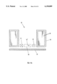
- FIG. 1a is a schematic view of one embodiment of the invention disposed in the differential sensor configuration
- FIG. 1b is a schematic view of an alternative embodiment of the invention disposed in the absolute sensor configuration
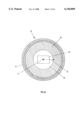
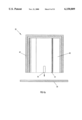
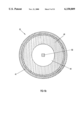
- FIG. 2a is a side sectional view of a coil induction embodiment of the invention, similar to the embodiment of FIG. 1a, configured to perform differential sensing;
- FIG. 2b is a top sectional view of the embodiment of FIG. 2a;
- FIG. 3 is a diagrammatic illustration of the operational routine of the embodiment of FIGS. 2a and 2b;
- FIG. 4a is a side sectional view of a coil induction embodiment of the invention configured to perform differential sensing
- FIG. 4b is a top sectional view of the embodiment of FIG. 4a;
- FIG. 5a is a side sectional view of a coil induction embodiment of the invention configured to perform passive absolute field sensing
- FIG. 5b is a top sectional view of the embodiment of FIG. 5a
- FIG. 6 is a diagrammatic illustration of the operational routine of the embodiment of FIGS. 5a and 5b;
- FIG. 7a is a side sectional view of a coil induction embodiment of the invention configured to perform absolute field sensing with active compensation for the magnetic field;
- FIG. 7b is a top sectional view of the embodiment of FIG. 7a;
- FIG. 8 is a diagrammatic illustration of the operational routine of the embodiment of FIGS. 7a and 7b;
- FIG. 9a is a side sectional view of a sheet induction embodiment of the apparatus of the invention with active field compensation
- FIG. 9b is a bottom view in partial section of the embodiment of FIG. 9a;
- FIG. 10 is a diagrammatic illustration of the operational routine of the embodiment of FIGS. 9a and 9b;
- FIG. 11a is a top sectional view of a ferromagnetic induction embodiment of the apparatus of the invention configured to perform curl sensing;
- FIG. 11b is a side sectional view of the embodiment of FIG. 11a;
- FIG. 12 is a diagrammatic illustration of the operational routine of the embodiment of FIGS. 11a and 11b;
- FIG. 13a is a top sectional view of a ferromagnetic induction embodiment of the apparatus of the invention configured to perform dual-differential field sensing;
- FIG. 13b is a side sectional view of the embodiment of FIG. 13a;
- FIG. 14 is a diagrammatic illustration of the operational routine of the embodiment of FIGS. 13a and 13b;
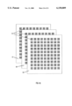
- FIG. 15 depicts a two dimensional array of GMR sensors on a single substrate useable in the apparatus of the invention
- FIG. 16 depicts a three dimensional array of GMR sensors on a plurality of substrates useable in the apparatus of the invention
- FIG. 17 is a side sectional view of a hand-held embodiment of a single-channel detector apparatus in a self-nulling configuration according to the present invention.
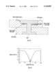
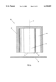
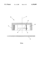
- FIG. 18 is a side sectional view of a crack in an aluminum sheet hidden under a rivet head and detectable by practicing the present invention.
- FIG. 19 graphically displays the plot of the giant magnetoresistance response for the material used to make a GMR sensor used in an embodiment of the apparatus of the invention
- FIG. 20 is a schematic diagram of a circuit useable to operate the GMR sensor and induction field according to the invention.
- FIG. 21 graphically displays data obtained using a single channel embodiment of the apparatus of the invention to detect a straight line cut in a single metal sheet;
- FIG. 22 graphically displays data obtained using a single channel embodiment of the apparatus of the invention to detect a crack hidden by an overlying metal sheet;
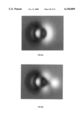
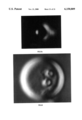
- FIGS. 23a, 23b and 23c are digital two dimensional images of data obtained using a single channel embodiment of the apparatus of the invention used with an x-y positioning table, illustrating a normal rivet, an anomalous rivet, and a rivet covering two cracks, respectively;
- FIG. 24 is a digital two dimensional image of data obtained using a single channel embodiment of the apparatus of the invention used with an x-y positioning table, illustrating corrosion hidden inside an aluminum sample.
- This invention relates to the use of magnetic field detection to perform non-destructive evaluation of conductive, typically but not necessarily metallic, components.
- conductive means electrically conductive unless otherwise indicated.
- changes in magnetic field attributable to flaws or discontinuities in the sampled component or structure may be detected without having to dis-assemble or destroy the component.
- the present invention uses one or more giant magnetoresistance sensors directly to detect a magnetic field induced in the material to be tested. It will be readily apparent that the invention finds beneficial application for corrosion and crack detection in metallic parts, eddy current measurements applied to NDE, manufacturing or other purposes. It is also useful for measurements related to thickness of films on metals including, but not limited to, paint thickness measurements.
- the invention is useable in manufacturing when flaws, pilot holes, and the presence of a material must be determined.
- the invention has applications in both chemistry and medicine, including uses in nuclear magnetic resonance (NMR) and magnetic resonance imaging (MRI).
- the giant magnetoresistance (GMR) phenomenon is a recently discovered effect occurring in metallic films consisting of magnetic layers a few nanometers thick separated by equally thin nonmagnetic layers. Large changes in the resistance of these films is observed when an external magnetic field is applied.
- the cause of this effect is the spin dependence of electron scattering and the spin polarization of conduction electrons in ferromagnetic metals. With layers of the proper thickness, adjacent magnetic layers couple antiferromagnetically to each other with the magnetic moments of each magnetic layer aligned antiparallel to the adjacent magnetic layers. Conduction electrons, spin polarized in one magnetic layer, are likely to be scattered as they reach the interface with an adjacent magnetic layer with antiparallel conduction electron spins. Frequent scattering results in high resistivity.
- the size of this decrease in resistivity can be 10% to 20% and higher in GMR materials with multiple nonmagnetic layers.
- Known systems utilizing eddy current sensors excite a drive coil and sense impedance changes in a coil due to induced eddy currents in a material under test (MUT).
- the detector of the present invention is significantly different from known eddy current sensors in that, among other differences, a GMR sensor detects induced field changes directly, rather than indirectly. Any changes in excitation field amplitude due to eddy current field interaction with the excitation coil adversely affects the information content in the detected output signal. An increase in eddy current field strength produces an increase in sensor output and also an increase in the impedance of the excitation winding.
- an impedance insensitive, constant field strength excitation circuit may be employed in the invention. This may be accomplished by using a constant amplitude sine wave signal to drive a precision wide band voltage to current converter with a current source impedance considerably in excess of the excitation coil impedance.
- the depth of penetration of a magnetic field into a material under test can be controlled by transducer geometry and signal frequency.
- a computer-controlled array of GMR sensors, tuned to the magnetic field frequency, can be used to scan large areas of a component rapidly with a high degree of spatial resolution. Data from the scanned area may be used to construct an image viewable on a portable video monitor, making possible the rapid detection of small anomalies in a variety of metallic components or structures.
- the combination of excellent signal to noise ratio, high spatial resolution, and depth profiling of the invention results in an NDE technology superior to existing systems, such as those based on conventional eddy current technologies and other technologies.
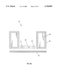
- FIG. 1a illustrates a basic differential sensor configuration of the detector apparatus 30 of the present invention.
- FIG. 1b shows an alternative, also basic, absolute sensor configuration of the detector apparatus 30 of the invention. Both configurations can be adapted to use single sensor element or sensor array-based systems.
- the GMR sensor 50 is a magnetic field-dependent resistance element usable singly, or in a shielded Wheatstone bridge configuration, or in a two- or three-dimensional array of sensor elements (FIGS. 15 and 16).
- Each GMR sensor 50 responds to permanent magnets, electromagnets, the earth's magnetic field for low field NMR measurements, or any other source of magnetic fields.
- the source of the applied magnetic filed may simply be the earth's magnetic field; thus, the earth itself may be a natural means for generating an applied magnetic field.
- FIGS. 1a and 1b In a GMR sensor 50, maximum sensor output occurs for fields originating along the "easy" or most sensitive axis 52 indicated by a directional arrow in FIGS. 1a and 1b. Response along the antiparallel "hard” axis is low, and response out of the plane of the GMR sensor 50 is very low.
- the present invention makes use of all the foregoing attributes.
- the differential configuration shown in FIG. 1a detects the induced magnetic field 26 orthogonal to the applied magnetic field 25.
- An electrically driven coil or solenoid 40 (with air, ferrite or other core) is used to generate the magnetic field 25 that is applied generally perpendicular to the material under test 20 (MUT).
- the GMR sensor 50 is positioned either inside the coil 40 or at the end of the coil 40 nearest the MUT 20.
- the sensitive axis 52 of the GMR sensor 50 is aligned orthogonal to the principal axis 41 of the coil 40. With the GMR sensor 50 thus positioned, the sensitive axis 52 is not aligned with the applied field 25 generated by the coil 40.
- This differential sensor configuration as shown in FIG. 1a, is best suited to the detection of cracks and pitting corrosion in the MUT 20.
- the absolute configuration of the apparatus 30 shown in FIG. 1b is similar, except that the sensitive axis 52 is aligned with or parallel to the principal axis 41 of the coil 40 and thus is substantially aligned with the applied field 25.
- the detector apparatus 30 can sense changes in thickness, and is well-suited to the detection of uniform, intergranular and exfoliation corrosion in the MUT 20.
- an active-feedback, loop-filter arrangement optionally may be used.
- the user preferably controls the output of a variable frequency oscillator by means of a central processing unit (CPU).
- the oscillator output is converted into a constant current signal by a constant current amplifier.
- the constant current amplifier prevents any changes in the interrogation signal resulting from impedance changes in the coil 40 caused by the material under test (MUT) 20.
- the constant current amplifier drives the field generation coil 40.
- the coil 40 may have an air core 44 or a core 44 fashioned of phenolic material, iron, ferrite or the like.
- An optional flux focusing cup 42 is made from materials such as mu metal or ferrite. The principal purpose of focusing cup 42 is to confine or restrict the induction field.
- FIGS. 2a and 2b illustrate that the GMR sensor 50 is at an end of the coil 40 and is placed in close proximity to the MUT 20; contact at the MUT surface closest to the GMR sensor 50 is desirable, but not necessary, and not shown in FIG. 2a for clarity of illustration.
- the applied magnetic field generated by the coil 40 interacts with the MUT 20.
- the GMR sensor 50 with its sensitive "easy" axis 52 orthogonal to the principal axis 41 of the coil 40, is positioned laterally so that the divergent components of the applied field (as seen at 25 in FIG. 1a) substantially cancel each other for self-nulling field detection, or with a finite offset for differential field detection.
- the applied field generated by the coil 40 causes eddy-current flow in the MUT 20, which induces an induced magnetic field (as seen at 26 in FIG. 1a). If the MUT 20 is uniform and undamaged to a depth equal to the "skin-depth" of the MUT, the divergent components of the induced field 26 substantially cancel at the GMR sensor 50 and no signal is generated by the GMR sensor 50, in the case of self-nulling detection or a finite offset for differential field detection.
- the "skin-depth" of the MUT is determined from known electrical and magnetic properties of the MUT 20, as well as the selected interrogation frequency of the detector apparatus 30.
- signaled changes in the resistance of the GMR sensor 50 are amplified by an embedded amplifier and then detected using either a True RMS meter attached to an analog-to-digital converter (A/D) or by the A/D converter directly.
- Alternative approaches for monitoring the output of the sensor 50 include measurements of voltage, current, resistance, impedance, and phase. The detected signal is then sent to the CPU for display to the user and optional storage within the CPU memory.
- FIGS. 4a and 4b illustrate an alternative embodiment of the detector apparatus 30 employing coil induction with a differential sensor configuration.
- This alternative embodiment is similar to the embodiment of FIGS. 2a and 2b, except that a "pancake" coil 46 is used in place of coil 40, an air core 44 is used exclusively, the GMR sensor 50 is located interiorly within the pancake coil 46, and the optional flux focusing cup 42 covers only the top portion of the detector apparatus 30.
- the sensitive axis 52 is orthogonal to the principal axis 41 of the pancake coil 46; FIG. 3 also diagrams the operation routine of the embodiment of FIGS. 4a and 4b.
- FIGS. 5a and 5b showing another embodiment of the detector apparatus 30, this embodiment employing solenoid induction but with the passive absolute field sensor configuration generally according to FIG. 1b.
- This embodiment is similar to the embodiment of FIGS. 2a and 2b with respect to magnetic field generation; however, the sensitive axis 52 of the GMR sensor 50 is disposed generally parallel to the principal axis 41 of the coil 40, and thus is substantially aligned with the applied magnetic field (25 in FIG. 1b), as indicated by the directional arrow of FIG. 5a.
- the GMR sensor 50 detects the absolute field resulting from the interaction of the applied field 25 with the induced field (26 in FIG. 1b). As indicated by reference to FIG.
- both the magnitude and the phase of the resulting signal response from the GMR sensor 50 are detected by a magnitude and phase detector known in the art and then input, by way of dual analog-to-digital converters, to the CPU.
- a magnitude and phase detector known in the art and then input, by way of dual analog-to-digital converters, to the CPU.
- FIGS. 7a and 7b show an alternative embodiment of the detector apparatus 30 employing solenoid induction with an absolute field configuration, and utilizing active compensation.
- the embodiment of FIGS. 7a and 7b is similar to the embodiment of FIGS. 5a and 5b in that it measures the absolute field; this embodiment differs, however, in the method of measuring the absolute field.
- the signals from the GMR sensor 50 are not processed directly, but rather are indirectly detected and processed.
- the embodiment of FIGS. 7a and 7b uses a pair of coils 40, 47.
- the field compensation coil 47 preferably is disposed coaxially within the field generation coil 40, and the field compensation coil 47 is disposed around the GMR sensor 50 so that the sensor 50 is interior to both coils 40, 47.
- the sensitive axis 52 of the GMR sensor 50 is parallel or collinear with the principal axis of the field generation coil 40.
- the outer field generation coil 40 generates the applied interrogation field, which is detected by the GMR sensor 50.
- Reference also to FIG. 8 illustrates that the output from the GMR sensor 50 is fed to a loop-filter feedback circuit, which drives a fast current amplifier by means of a drive voltage sensor.
- the fast current amplifier in turn drives a field compensation coil 47, which generates a compensation field counteractive to the applied field such that the effective field sensed by the GMR sensor 50 is zero.
- the analog-to-digital converter monitors the driving voltage input to the fast current amplifier, rather than the signal output from the GMR sensor 50.
- This active compensation embodiment allows much larger interrogation field amplitudes to be used, relative to the previously described passive embodiments.
- FIGS. 9a and 9b show a detector apparatus 30 employing sheet induction with active compensation.
- this embodiment of detector 30 is similar to the embodiment of FIGS. 7a and 7b, but this embodiment employs a current sheet induction scheme.
- the GMR sensor 50 is disposed generally parallel between a substantially planar conductive drive sheet 54 and a substantially planar conductive compensation sheet 56 generally parallel thereto.
- Current (indicated by the circled Xs in FIG. 9a) is driven, through both the drive sheet 54 and the compensation sheet 56, generating two magnetic fields, an applied field and a compensative field, respectively. These resulting magnetic fields add in the regions exterior to the GMR sensor 50, and counteract to substantially cancel each other in the layer containing the GMR sensor 50.
- FIGS. 9a, 9b and 10 shows that the net magnetic field is detected by the GMR sensor 50, whose responsive signal drives a loop-filter compensation circuit similar to the circuitry of the FIG. 8 embodiment.
- a fast current amplifier drives the compensation sheet 56, such that the effective field sensed by the GMR sensor 50 is zero.
- the analog-to-digital converter monitors the driving voltage input to the fast current amplifier, rather than the output from the GMR sensor 50, and the current to the compensation sheet 56 is modified to cancel substantially the net field at the GMR sensor 50 and the input voltage to the fast current amplifier is monitored by the A/D converter, whereby the signal response of the GMR sensor 50 is only indirectly processed to yield final NDE data.
- the response signal from the GMR is not directly processed into information regarding the material under test; rather, a looped feedback circuit is employed whereby the response signal (i.e. change in resistance) output by the GMR sensor drives the compensative field, and a voltage input necessary to counteract or compensate the applied field is monitored to provide the necessary data regarding the material under test.
- the apparatus of the invention indirectly processes the signaled changes in the resistance of the GMR sensor to accomplish the task of detecting changes in the induced field.
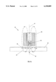
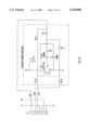
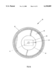
- FIGS. 11a, 11b and 12 show a detector apparatus 30 with ferromagnetic induction and configured to sense field curl.
- a constant current amplifier drives a ferromagnetic inductor including a winding of wire 58 wrapped around a ferrite core 59, thereby generating a large applied magnetic field.
- a rotating, scanning magnetic field may be generated in the MUT if ferrite 59 is a toroid perpendicular to the surface having both longitudinal and toroidal windings 58.
- the principal axis of the resultant field in the MUT 20 can be oriented at, or swept through, any angle relative to the sensor positions.
- the MUT 20 is ferrous and responds to the applied field with a "mirror" induced field.
- the interactions between the two fields are detected using at least two, preferably four or more, GMR sensors 50, 60, 61, 62 surrounded by the ferrite core 59.
- GMR sensors 50, 60, 61, or 62 Within the component of the net field sensed by each GMR sensor 50, 60, 61, or 62 is the curl generated by a large, changing electric field within the ferrite core 59.
- Reference to FIG. 12 illustrates that an instrument system utilizing a CPU controls the variable frequency oscillator, the output of which controls a constant current amplifier which in turn feeds electrical current to the ferromagnetic inductor.
- the inductor induces fields in the ferrous material under test 20.
- the GMR sensors 50, 60, 61, 62 are geometrically disposed such that the sensitive axes 52, 52' of at least two opposing sensors (e.g. 50, 60) are parallel, as seen in FIG. 11a.
- induced fields in the MUT 20 affect the GMR sensors 50, 60, 61, 62, which send signals to a summing circuit of known construction which adds the signals from the GMR sensors, whereby optimal sensitivity is achieved regardless of the positional relation of any defect in the MUT 20 with respect to the GMR sensors 50, 60, 61, 62.
- the summed signal is sent to a true RMS detector that conditions the signal voltages coming from the summation circuit, providing a voltage corresponding to the magnitude of the defect detected.
- An A/D converter converts the voltage corresponding to signal magnitude to a digital word readable by the CPU.
- the CPU performs automated data analysis on the sensor data for use in NDE, manufacturing or other applications.
- FIGS. 13a, 13b and 14 show a ferromagnetic induction detector apparatus 30 of the invention, with dual-differential detection.
- the physical portion of this embodiment is very similar to the embodiment of FIGS. 11a and 11b.
- a difference between the embodiment of FIGS. 11a and 11b and this embodiment is in the GMR sensor signal processing.
- the dual-differential configuration of the apparatus 30 uses differential detection to sense the differences in responsive signal magnitude from opposing pairs of GMR sensors, such as pairs of sensors 50, 60 and 61, 62 in FIG. 13a, to provide specific information regarding geometric symmetry within the MUT 20.
- the sensitive axes of at least one pair, and preferably two pair, of opposing sensors disposed generally parallel, any discontinuity in the MUT 20 results in an incomplete cancellation between the paired sensors 50, 60 or 61, 62.
- FIG. 14 shows that signals from opposing pairs of sensors 50, 60 and 61, 62 are input into respective differential detectors of known construction, each of which in turn provides input into a separate True RMS detector.
- Reference to FIG. 14 also illustrates that a CPU controls the variable frequency oscillator, the output of which controls a constant current amplifier which in turn feeds electrical current to the ferromagnetic inductor.
- the inductor induces fields in the ferrous material under test 20.
- the GMR sensors 50, 60, 61, 62 are placed in a geometry such that the sensitive axes of at least two, and preferably two or more pairs, of opposing sensors (e.g. 50, 60 and 61, 62) are parallel to one another (FIG. 13a).
- the magnetic fields induced in the MUT 20 cause the GMR sensors 50, 60, 61, 62, which are configured in a dual differential mode, to output responsive signals.
- Amplified output signals from the opposing pairs of GMR sensors are fed to the differential detector circuits which output the difference in magnitude between the associated pair of GMR sensors 50, 60 or 61, 62. If, for example, both sensors of a pair 50, 60 or 61, 62 respond equally to spurious noise, this configuration of the detector apparatus 30 cancels the output due to noise.
- This embodiment of the detector apparatus 30 also provides information concerning the geometry of defects in the MUT 20, since the larger size or closer proximity of a defect to any single one of the GMR sensors results in a larger signal from that sensor and consequently a larger differential signal for the corresponding sensor pair 50, 60 or 61, 62.
- Another advantage of this embodiment over four or more single GMR sensors is that the noise cancellation properties of the configuration make it possible to discern smaller defects in the MUT 20.
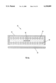
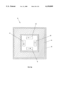
- FIG. 15 shows a two-dimensional array of a plurality of GMR sensors 50 on a single substrate 64.
- Such an array may be fabricated using a variety of techniques, with the GMR sensor elements 50 having spin valve, tunnel junction or other device configurations.
- the sensor elements 50 may be formed on solid substrates such as silicon wafers, or flexible substrates such as polyimide. Data from the array of GMR sensors 50 is read by computer for the purpose of making two dimensional images of a object in a magnetic field.
- Such a two-dimensional array of GMR sensors 50 may be used in any of the embodiments of the detector apparatus 30 depicted in FIGS. 3-14.
- FIG. 16 shows that a three dimensional array of GMR sensor elements 50 may be embedded in a sandwich structure having a plurality of layers.
- an array can be fabricated using a variety of techniques with the GMR sensors 50 having spin valve, tunnel junction or other device configurations.
- the GMR sensor elements 50 can be formed on a plurality of two or more (three shown in FIG. 16) solid substrates 64, 66, 67 such as silicon wafers, or flexible substrates such as polyimide. Data from the arrays is read by computer for the purpose of making three dimensional images of an object in a magnetic field.
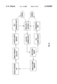
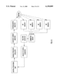
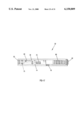
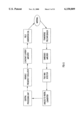
- FIG. 17 showing a single channel NDE detector apparatus 32 based on GMR sensors using the self-nulling configuration.
- a GMR sensor 50 is used for detection of magnetic fields.
- a central processing unit (CPU) 70 controls an oscillator and amplifier 69 which drive a coil for the induction of magnetic fields in the MUT 20.
- the sensor 50 responds to the magnetic fields induced in the MUT and outputs an electrical signal that is fed to a preamplifier and signal conditioning amplifier 75 and then an analog filter section 74.
- the amplified and conditioned sensor signal is fed to an A/D converter and then to the CPU 70 for digital signal processing and data analysis.
- the CPU 70 sends data to a external computer using a serial port 78.
- the apparatus 32 also has visual LCD and audible outputs 82.
- the apparatus is run by rechargeable batteries 80 for portable operation.
- Two spin valve GMR sensor arrays were fabricated on 2-inch diameter Silicon wafers. Small pieces were cleaved from each wafer to perform magnetic and transport characterization. The deposition parameters for both structures were nominally identical. The deposition layer thicknesses were as follows:
- Si/Si/Ox/NiO 500 ⁇ )/Co (5 ⁇ )/NiFe (35 ⁇ )/Cu (35 ⁇ )/Co (5 ⁇ )/NiFe (50 ⁇ ).
- Magnetization curves and magneto-resistance curves for the two devices were made to evaluate the high field behavior in both the hard and easy (sensitive) axis directions as well as the low field behavior along the easy axis.
- the easy axis is defined by the field applied during the deposition.
- the highest GMR sensitivity occurs when the field is applied along the easy axis.
- the reversal along the easy axis occurs through domain wall motion and thus can be rather noisy.
- a 4 ⁇ 4 array of GMR sensors was formed on each wafer by cutting shallow grooves in the surface with a diamond scribe.
- the sheet resistance was roughly 80 ohms per square.
- the inter-sensor resistance on the wafer was about 1000 ohms due to conduction through the silicon. This level of resistance is high enough to permit detection of the individual responses of the sensors while on the silicon substrate. The feasibility of a functional GMR sensor array on a single silicon substrate (e.g. as seen in FIG. 15) is thus demonstrated.
- GMR sensors on a silicon substrate had multilayer sheet resistance of about 10 ohms per square, and resistor legs on silicon 2 microns across. These properties allow the construction of a 10K resistor in an area of 80 microns by 100 microns (using 2 micron lithography). The sensors were housed in an 8-pin surface mount SOIC package. Two of the more sensitive devices had resistance changes of 9.81% and 9.74% for the sense resistors with saturation at 15 Oe resulting in a sensitivity of 0.64%/Oe. At a nominal bridge bias voltage of 5V, the measured bridge sensitivity was 4.0 mV/VOe with an element resistance of 3.92K.
- FIG. 19 A plot of the GMR response for the material used to make the sensors is shown in FIG. 19. The measurement was made with a four point probe, 5 volt bias.
- the Wheatstone bridge is advantageous for DC measurements where a significant DC offset makes the measurement of small DC signals difficult.
- the DC offsets are easily eliminated with a simple filter.
- the impedance of the Wheatstone bridge itself can present problems with signal degradation, particularly at higher frequencies. Studies showed that signal quality was good up to approximately 1 MHZ with the Wheatstone bridge configuration.
- the use of flux concentrators essentially increase the sensitivity of the GMR material by some concentration factor of from 2 to 100.
- the flux concentration factor is roughly equivalent to the length of one shield divided by the length of the gap between the shields.
- tailored flux concentrators could substantially increase the low field sensitivity of GMR sensors designed specifically for NDE.
- the output of the GMR sensor was fed to an amplifier circuit and data collected with a digital oscilloscope and a PC.
- This raw data consisted of voltages corresponding to the magnetic field strength at selected points on the material under test.
- the material test samples used during the development of the inventive apparatus consisted of sheets of aluminum and steel alloy selected to mimic components such as aircraft structures. The samples had cracks or cuts in the range of 0 to 100 ⁇ m and the GMR sensors were tested for the ability to locate these known "defects.”
- the final GMR sensor optimized for the NDE measurements consisted of an Wheatstone bridge surrounded by a 55 ⁇ H excitation winding (90 turns, 6 layers pi wound, 7/32" ID, 0.42" OD, 0.12" high).
- the bridge and coil were placed on smooth, flat, defect-free sheets of 2024T3 aluminum and the coil driven to produce a 13 Oe peak field at 12 kHz.
- the bridge was orientated for minimum residual signal (i.e. generally perpendicular to the coil axis) and potted in place.
- the schematic of the circuitry utilized appears in FIG. 20.
- Metal test samples were evaluated by affixing the material under test to a computer controlled, precision positioning mechanism and scanning the sample with the GMR sensor.
- the positioning mechanism controlled the distance between each measurement to ⁇ 10 ⁇ m.
- the output of the GMR sensor was fed to an amplifier circuit and data collected with a digital oscilloscope and a personal computer (PC). This raw data consisted of voltages corresponding to the magnetic field strength at selected points on the test samples.
- the GMR sensor apparatus optimized for the NDE measurements consisted of a Wheatstone bridge sensor arrangement surrounded by a 55 ⁇ H excitation winding.
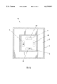
- FIG. 18 is an illustration of a cross-section of a rivet site showing the types of cracks that occur.
- the prototype apparatus was evaluated for its ability to detect defects in a number of different materials including alloys of both aluminum and steel. Analysis was performed to determine the effects of the type of material under study, the dimensions and depth of the defect, and the effects of overlying metal on the detection of a defect.
- a set of sample plates were cut using EDM to form a set of arcs with 1", 1/2", 1/4", and 1/8" diameters.
- a similar set of test samples were cut with straight lines 1/2", 1/4", 1/8", and 1/16" long. All of the cuts had a nominal width of 100 ⁇ m.
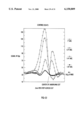
- FIGS. 21 and 22 show the sensor response for a 2024 aluminum sheet with 100 ⁇ m wide linear cuts of various lengths (1/16 inch, 1/8 inch, 1/4 inch, and 1/2 inch). The baseline was extremely flat where no cut existed, and the signal to noise (S/N) ratio was in excess of 80 even for the 1/8-inch long cut.
- FIG. 22 shows the response for arc-shaped cuts in a covered panel, in similitude of the type of damage sought to be detected around rivets. All of the arc-shaped cuts were detectable in the lower 2024 aluminum panel, as indicated by the nadir in the graphical display.
- the signal amplitude from the GMR sensor system was extremely constant when no cut was present. As the edge of a cut was approached my the moving sensor, the locally induced magnet fields were concentrated and curved. This effect was detected by the GMR sensors and resulted in an increase in signal amplitude. By mapping the signal amplitude and position throughout a scan, it was possible to locate minute cuts in the material with a high level of confidence.
- an aircraft material sample was obtained from an FAA facility consisting of two 2024 aluminum sheets [48 mils (1225 ⁇ m) and 74 mils (1870 ⁇ m) thick] riveted together with 2024 aluminum rivets.
- the rivets had 0.0625 inch diameter shafts with 0.24 inch diameter heads and 1 inch nominal spacing between rivets.
- FIG. 23a and FIG. 23b The resulting images of an inspection of a normal rivet and an anomalous rivet with two cracks are depicted in FIG. 23a and FIG. 23b, respectively.
- FIG. 21c shows a composite image resulting from the subtraction of the normal rivet image from the anomalous rivet image.
- the composite image of FIG. 23c provides a simple and intuitive assessment indication of the presence of a damaged part (rivet), illustrating the type of images and image enhancements obtainable with the invention.
- FIGS. 21a, 21c, and 21c the mechanical deformations and cracks associated with the rivets are clearly visible.
- the S/N ratio was extremely high with a very low noise level away from the riveted areas.
- the test showed that it is possible to image cracks that are underneath the rivet head and therefore undetectable with visual inspection.
- FIG. 24 depicts data from a single channel NDE corrosion detector taken with an x-y positioning table to yield a two dimensional image of corrosion hidden inside an aluminum sample.
Abstract
Description
Claims (24)
Priority Applications (3)
| Application Number | Priority Date | Filing Date | Title |
|---|---|---|---|
| US08/932,843 US6150809A (en) | 1996-09-20 | 1997-09-18 | Giant magnetorestive sensors and sensor arrays for detection and imaging of anomalies in conductive materials |
| PCT/US1997/016847 WO1998012554A1 (en) | 1996-09-20 | 1997-09-19 | Gmr-based detection of defects in conducting materials |
| AU46478/97A AU4647897A (en) | 1996-09-20 | 1997-09-19 | Gmr-based detection of defects in conducting materials |
Applications Claiming Priority (2)
| Application Number | Priority Date | Filing Date | Title |
|---|---|---|---|
| US2642496P | 1996-09-20 | 1996-09-20 | |
| US08/932,843 US6150809A (en) | 1996-09-20 | 1997-09-18 | Giant magnetorestive sensors and sensor arrays for detection and imaging of anomalies in conductive materials |
Publications (1)
| Publication Number | Publication Date |
|---|---|
| US6150809A true US6150809A (en) | 2000-11-21 |
Family
ID=26701228
Family Applications (1)
| Application Number | Title | Priority Date | Filing Date |
|---|---|---|---|
| US08/932,843 Expired - Lifetime US6150809A (en) | 1996-09-20 | 1997-09-18 | Giant magnetorestive sensors and sensor arrays for detection and imaging of anomalies in conductive materials |
Country Status (3)
| Country | Link |
|---|---|
| US (1) | US6150809A (en) |
| AU (1) | AU4647897A (en) |
| WO (1) | WO1998012554A1 (en) |
Cited By (112)
| Publication number | Priority date | Publication date | Assignee | Title |
|---|---|---|---|---|
| WO2001067085A1 (en) * | 2000-03-07 | 2001-09-13 | Teodor Dogaru | Probe for eddy current testing |
| US20020107456A1 (en) * | 2000-08-01 | 2002-08-08 | L'oreal | Method of acquiring an image of a non-dermatoglyphic zone of the skin or of a zone of the hair by means of acquisition apparatus including a non-optical sensor |
| US20020158626A1 (en) * | 2000-11-08 | 2002-10-31 | Jentek Sensors, Inc. | Deep penetration magnetoquasistatic arrays |
| US20030011363A1 (en) * | 2001-05-30 | 2003-01-16 | Malcolm Wayman | Pipe condition detecting apparatus |
| EP1306667A1 (en) * | 2001-10-29 | 2003-05-02 | Cegelec | Sensor for detection of defects in a metallic sample by use of eddy currents |
| US6583617B2 (en) * | 2000-08-24 | 2003-06-24 | Kemp Corporation | Barkhausen noise measurement probe with magnetoresistive sensor and cylindrical magnetic shield |
| US20030164698A1 (en) * | 2001-01-29 | 2003-09-04 | Paulson Peter O | Electromagnetic analysis of concrete tensioning wires |
| US6625554B2 (en) * | 2001-06-22 | 2003-09-23 | Hitachi, Ltd. | Method and apparatus for determining a magnetic field |
| US6657431B2 (en) * | 2000-06-06 | 2003-12-02 | Brown University Research Foundation | Scanning magnetic microscope having improved magnetic sensor |
| US6657439B1 (en) * | 1999-04-28 | 2003-12-02 | Sharp Kabushiki Kaisha | Sheet resisitance meter |
| US20040041560A1 (en) * | 2002-08-28 | 2004-03-04 | Scan Systems Corp. | Method, system and apparatus for ferromagnetic wall monitoring |
| US6720775B2 (en) * | 2001-06-12 | 2004-04-13 | General Electric Company | Pulsed eddy current two-dimensional sensor array inspection probe and system |
| US6724192B1 (en) * | 1997-09-10 | 2004-04-20 | T. David McGlone | Method and apparatus for exploration using GMR sensors |
| US6734660B1 (en) * | 2002-02-07 | 2004-05-11 | Lockheed Martin Corporation | Current sensor arrangement with test current generator |
| WO2004055490A1 (en) * | 2002-12-18 | 2004-07-01 | Security Control S.R.L. | Magnetic-inductive device for the control of ferromagnetic reticles |
| FR2851337A1 (en) * | 2003-02-19 | 2004-08-20 | Cegelec | Fault detector for component with conducting material has polarization circuit with electrical conductor close to magneto resistor |
| US20040178267A1 (en) * | 2003-03-11 | 2004-09-16 | Zebra Technologies Corporation | System and Method for Selective Communication with RFID Transponders |
| US20040196681A1 (en) * | 2002-03-25 | 2004-10-07 | Gang Xiao | Reduction of noise, and optimization of magnetic field sensitivity and electrical properties in magnetic tunnel junction devices |
| US6822443B1 (en) | 2000-09-11 | 2004-11-23 | Albany Instruments, Inc. | Sensors and probes for mapping electromagnetic fields |
| US20040232909A1 (en) * | 2001-09-25 | 2004-11-25 | Kazunobu Imamoto | Non-destructive inspection device and non-destructive inspection method |
| US20040245997A1 (en) * | 2001-06-12 | 2004-12-09 | Plotnikov Yuri Alexeyevich | Pulsed eddy current sensor probes and inspection methods |
| US20050007108A1 (en) * | 2003-07-11 | 2005-01-13 | Teodor Dogaru | Probes and methods for detecting defects in metallic structures |
| US6888346B2 (en) | 2000-11-28 | 2005-05-03 | The United States Of America As Represented By The Administrator Of The National Aeronautics And Space Administration | Magnetoresistive flux focusing eddy current flaw detection |
| US20050140355A1 (en) * | 2003-07-22 | 2005-06-30 | Kanazawa University | Eddy-current sensor for nondestructive testing |
| US20050269409A1 (en) * | 2004-06-04 | 2005-12-08 | Perner Fredrick A | Magnetic stripline scanner |
| US20050280411A1 (en) * | 2004-06-16 | 2005-12-22 | Bicking Robert E | GMR sensor with flux concentrators |
| US20050286607A1 (en) * | 2004-06-28 | 2005-12-29 | Samsung Electronics Co., Ltd. | Temperature measuring apparatus using change of magnetic field |
| US20060006864A1 (en) * | 2004-07-08 | 2006-01-12 | Honeywell International, Inc. | Integrated magnetoresitive speed and direction sensor |
| US20060025390A1 (en) * | 2004-07-28 | 2006-02-02 | Roby Russell R | Treatment of hormone allergy and related symptoms and disorders |
| US20060038558A1 (en) * | 2004-08-20 | 2006-02-23 | The Boeing Company | Eddy current inspection device |
| US20060170420A1 (en) * | 2005-01-12 | 2006-08-03 | Akira Nishimizu | Eddy current testing probe and eddy current testing apparatus |
| US20060173295A1 (en) * | 2005-01-26 | 2006-08-03 | Zeijlemaker Volkert A | Apparatus for detecting strong magnetic fields for protection of medical devices |
| US20060192123A1 (en) * | 2004-12-16 | 2006-08-31 | Michel Hamelin | Crack detection in razor blades |
| US20060206025A1 (en) * | 2005-03-08 | 2006-09-14 | Siemens Westinghouse Power Corporation | Inspection of composite components using magnetic resonance imaging |
| US7145330B2 (en) | 2002-08-16 | 2006-12-05 | Brown University Research Foundation | Scanning magnetic microscope having improved magnetic sensor |
| US20070090825A1 (en) * | 2005-09-30 | 2007-04-26 | Tdk Corporation | Current sensor |
| US20070100579A1 (en) * | 2005-10-31 | 2007-05-03 | The Boeing Company | Control for hand-held imaging array using computer mouse configuration |
| US20070096727A1 (en) * | 2005-11-01 | 2007-05-03 | The Boeing Company | Flexible hand held mr scanning array for cracks/flaws |
| US20070120560A1 (en) * | 2005-11-29 | 2007-05-31 | The Boeing Company | Eddy current inspection device with arrays of magnetoresistive sensors |
| US20070222433A1 (en) * | 2006-03-21 | 2007-09-27 | Radiation Monitoring Devices, Inc. | Sensor array for nuclear magnetic resonance imaging systems and method |
| US20070299333A1 (en) * | 2003-01-17 | 2007-12-27 | Mednovus, Inc. | Magnetic resonance imaging screening method |
| US20080040053A1 (en) * | 2006-08-10 | 2008-02-14 | General Electric Company | Inspection systems and methods of operation |
| US20080094798A1 (en) * | 2005-04-11 | 2008-04-24 | Lee Sang C | Apparatus for cooling computer parts and method of manufacturing the same |
| WO2008054056A1 (en) * | 2006-11-01 | 2008-05-08 | Industry-Academic Cooperation Foundation, Chosun University | Magnetic sensor array and apparatus for detecting defect using the magnetic sensor array |
| WO2007056679A3 (en) * | 2005-11-03 | 2008-05-29 | Clock Spring Company L P | Comformable eddy current array |
| US20080143328A1 (en) * | 2005-02-28 | 2008-06-19 | Klaus Thierauf | Method and Device for Measuring the Magnetic Properties of Documents |
| US20080151435A1 (en) * | 2006-12-26 | 2008-06-26 | Fujitsu Limited | Storage apparatus, method of detecting failure in head of storage apparatus, and storage medium storing failure detection program |
| US7397238B2 (en) | 2005-07-28 | 2008-07-08 | Walters William T | Methods and apparatus for inspecting materials |
| US20080298822A1 (en) * | 2007-05-30 | 2008-12-04 | Zih Corp. | System for processing media units and an associated media roll |
| US20090066326A1 (en) * | 2006-05-09 | 2009-03-12 | Fujikura Ltd. | Magnetic device |
| US20090115410A1 (en) * | 2007-11-05 | 2009-05-07 | Mcknight William Stewart | Eddy current probe and methods of assembling the same |
| US20090115411A1 (en) * | 2007-11-05 | 2009-05-07 | Haiyan Sun | Flexible eddy current array probe and methods of assembling the same |
| US20090162123A1 (en) * | 2007-12-19 | 2009-06-25 | Zih Corp. | Platen incorporating an rfid coupling device |
| US20100123453A1 (en) * | 2008-11-19 | 2010-05-20 | Nokomis, Inc. | Advance manufacturing monitoring and diagnostic tool |
| US20100127699A1 (en) * | 2008-11-25 | 2010-05-27 | General Electric Company | System and method for inspection of parts with complex geometries |
| US20100308830A1 (en) * | 2009-06-05 | 2010-12-09 | Ira Shankar | Magnetic field detection device |
| US20110084926A1 (en) * | 2009-10-09 | 2011-04-14 | Egalax_Empia Technology Inc. | Method and device for converting sensing information |
| US20110084937A1 (en) * | 2009-10-09 | 2011-04-14 | Egalax_Empia Technology Inc. | Method and device for analyzing positions |
| US20110084936A1 (en) * | 2009-10-09 | 2011-04-14 | Egalax_Empia Technology Inc. | Method and device for capacitive position detection |
| US20110084929A1 (en) * | 2009-10-09 | 2011-04-14 | Egalax_Empia Technology Inc. | Method and device for position detection |
| US20110084930A1 (en) * | 2009-10-09 | 2011-04-14 | Egalax_Empia Technology Inc. | Method and device for dual-differential sensing |
| US20120153947A1 (en) * | 2010-12-15 | 2012-06-21 | Udo Ausserlechner | Magnetoresistive angle sensors |
| WO2012092467A2 (en) * | 2010-12-29 | 2012-07-05 | Methode Electronics, Inc. | Sensor arrangements for measuring magnetic susceptibility |
| CN102621219A (en) * | 2011-01-28 | 2012-08-01 | 通用电气检查技术有限公司 | A non-destructive test method for automatic fastener inspection |
| US20120330491A1 (en) * | 2010-10-05 | 2012-12-27 | Olinger Michael D | Automatic guided vehicle sensor system and method of using same |
| US20130193960A1 (en) * | 2012-01-27 | 2013-08-01 | Hitachi-Ge Nuclear Energy, Ltd. | Eddy Current Flaw Detection System and Eddy Current Flaw Detection Method |
| US20140002070A1 (en) * | 2012-06-29 | 2014-01-02 | Zetec, Inc. | Axial and circumferential flaw sensing eddy current probe |
| US20140116131A1 (en) * | 2012-11-01 | 2014-05-01 | Ti Group Automotive Systems, L.L.C. | Contactless liquid level sensor |
| US8841904B1 (en) * | 2011-02-17 | 2014-09-23 | The Boeing Company | Nondestructive inspection probe and method |
| US8872776B2 (en) | 2009-10-09 | 2014-10-28 | Egalax—Empia Technology Inc. | Method and device for analyzing two-dimension sensing information |
| US8970217B1 (en) | 2010-04-14 | 2015-03-03 | Hypres, Inc. | System and method for noise reduction in magnetic resonance imaging |
| US20150077151A1 (en) * | 2013-09-13 | 2015-03-19 | Infineon Technologies Ag | Apparatus and Method for Testing Electric Conductors |
| US20150084663A1 (en) * | 2012-06-12 | 2015-03-26 | Dow Global Technologies Llc | Method and apparatus for detecting discontinuitues in a solar array |
| US20150239708A1 (en) * | 2014-02-25 | 2015-08-27 | Thyssenkrupp Elevator Ag | System and Method for Monitoring a Load Bearing Member |
| US9285940B2 (en) | 2009-10-09 | 2016-03-15 | Egalax—Empia Technology Inc. | Method and device for position detection |
| US20160109408A1 (en) * | 2013-05-10 | 2016-04-21 | Commissariat A L'energie Atomique Et Aux Energies Alternatives | Inspection head of an eddy current non-destructive testing sensor and sensor comprising such an inspection head |
| US9395418B2 (en) | 2011-06-13 | 2016-07-19 | Methode Electronics, Inc. | System and method for determining the state of health of electrochemical battery cells |
| US9470657B2 (en) | 2012-10-04 | 2016-10-18 | Her Majesty The Queen In Right Of Canada As Represented By The Minister Of Natural Resources Canada | Measurement of lay length of wire rope |
| US20160341803A1 (en) * | 2014-01-31 | 2016-11-24 | University Of South Australia | Sensor for detection of magnetic particles |
| US20160356735A1 (en) * | 2015-06-04 | 2016-12-08 | Grid Logic Incorporated | Nondestructive tester |
| CN106324044A (en) * | 2016-08-22 | 2017-01-11 | 华北电力大学 | Device and method for detecting metal oxygen carrier in combustion process of chemical chain |
| US9618591B1 (en) | 2009-11-24 | 2017-04-11 | Hypres, Inc. | Magnetic resonance system and method employing a digital squid |
| WO2017138972A1 (en) * | 2015-02-11 | 2017-08-17 | Structural Integrity Associates, Inc. | Dynamic pulsed eddy current probe |
| US9784715B2 (en) | 2013-04-19 | 2017-10-10 | Zetec, Inc. | Eddy current inspection probe based on magnetoresistive sensors |
| US9823179B2 (en) | 2011-10-25 | 2017-11-21 | Jentek Sensors, Inc. | Method and apparatus for inspection of corrosion and other defects through insulation |
| US9864471B2 (en) | 2009-10-09 | 2018-01-09 | Egalax_Empia Technology Inc. | Method and processor for analyzing two-dimension information |
| EP3159854A4 (en) * | 2014-06-23 | 2018-02-28 | Multidimension Technology Co., Ltd. | Coin detection system |
| WO2018093855A1 (en) * | 2016-11-16 | 2018-05-24 | 3M Innovative Properties Company | Verifying structural integrity of materials using magnetic field stimulation |
| US20180202975A1 (en) * | 2015-07-16 | 2018-07-19 | Sumitomo Chemical Company, Limited | Defect measurement method, defect measurement device, and testing probe |
| US20180275671A1 (en) * | 2016-12-23 | 2018-09-27 | Gecko Robotics, Inc. | System, method, and apparatus to perform a surface inspection using real-time position information |
| CN108802170A (en) * | 2017-04-28 | 2018-11-13 | 中国科学院大学 | A kind of electromechanical detection method of whole audience formula defect using electronic speckle technology |
| US20180340987A1 (en) * | 2017-05-26 | 2018-11-29 | Allegro Microsystems, Llc | Packages For Coil Actuated Position Sensors |
| US10416244B2 (en) | 2016-09-28 | 2019-09-17 | Arizona Board Of Regents On Behalf Of Arizona State University | Three-dimensional imaging utilizing low frequency magnetic fields |
| US10448864B1 (en) | 2017-02-24 | 2019-10-22 | Nokomis, Inc. | Apparatus and method to identify and measure gas concentrations |
| US10539535B2 (en) | 2015-07-16 | 2020-01-21 | Sumitomo Chemical Company, Limited | Defect measurement method, defect measurement device, and testing probe |
| US10816495B2 (en) | 2016-12-16 | 2020-10-27 | 3M Innovative Properties Company | Verifying structural integrity of materials |
| US10895555B2 (en) | 2015-03-30 | 2021-01-19 | Structural Integrity Associates, Inc. | System for in-line inspection using a dynamic pulsed eddy current probe and method thereof |
| US10983081B2 (en) | 2016-11-16 | 2021-04-20 | 3M Innovative Properties Company | Electrode placement for verifying structural integrity of materials |
| US11009484B1 (en) | 2016-03-11 | 2021-05-18 | The University Of Tulsa | Velocity independent two-component magnetic flux leakage detective system |
| US11054318B2 (en) * | 2017-06-14 | 2021-07-06 | Rolls-Royce Corporation | System for nondestructive residual stress profiling using inductive sensing |
| US11060993B2 (en) | 2016-11-16 | 2021-07-13 | 3M Innovative Properties Company | Suppressing thermally induced voltages for verifying structural integrity of materials |
| US11105762B2 (en) | 2016-12-16 | 2021-08-31 | 3M Innovative Properties Company | Verifying structural integrity of materials using reference impedance |
| US11112374B2 (en) | 2016-12-16 | 2021-09-07 | 3M Innovative Properties Company | Verifying structural integrity of materials |
| US11135721B2 (en) | 2016-12-23 | 2021-10-05 | Gecko Robotics, Inc. | Apparatus for providing an interactive inspection map |
| US11181498B2 (en) | 2016-11-16 | 2021-11-23 | 3M Innovative Propperties Company | Temperature-independent verifying of structural integrity of materials using electrical properties |
| US11249047B2 (en) * | 2015-08-31 | 2022-02-15 | Siemens Mobility Pty Ltd. | Method and system for detecting a material discontinuity in a magnetisable article |
| US11255807B2 (en) | 2016-11-16 | 2022-02-22 | 3M Innovative Properties Company | Verifying structural integrity of materials |
| US11307063B2 (en) | 2016-12-23 | 2022-04-19 | Gtc Law Group Pc & Affiliates | Inspection robot for horizontal tube inspection having vertically positionable sensor carriage |
| US20220214290A1 (en) * | 2021-01-05 | 2022-07-07 | The Boeing Company | Methods and apparatus for measuring fastener concentricity |
| US11489847B1 (en) | 2018-02-14 | 2022-11-01 | Nokomis, Inc. | System and method for physically detecting, identifying, and diagnosing medical electronic devices connectable to a network |
| US11813672B2 (en) | 2020-05-08 | 2023-11-14 | Grid Logic Incorporated | System and method for manufacturing a part |
| US11850726B2 (en) | 2021-04-20 | 2023-12-26 | Gecko Robotics, Inc. | Inspection robots with configurable interface plates |
Families Citing this family (7)
| Publication number | Priority date | Publication date | Assignee | Title |
|---|---|---|---|---|
| US6411084B1 (en) * | 1999-04-05 | 2002-06-25 | Halliburton Energy Services, Inc. | Magnetically activated well tool |
| US6815946B2 (en) | 1999-04-05 | 2004-11-09 | Halliburton Energy Services, Inc. | Magnetically activated well tool |
| US8497459B2 (en) | 2010-01-08 | 2013-07-30 | Washington University | Method and apparatus for high resolution photon detection based on extraordinary optoconductance (EOC) effects |
| EP2154540B1 (en) * | 2006-08-01 | 2014-12-31 | Washington University | Multifunctional nanoscopy for imaging cells |
| CN109884129B (en) * | 2019-03-27 | 2021-11-23 | 爱德森(厦门)电子有限公司 | Device and method for detecting thermite welding quality of steel rail |
| US11346811B1 (en) * | 2021-09-30 | 2022-05-31 | United States Pipe And Foundry Company, Llc | Method and apparatus for identifying discontinuity in wall of ferrous object |
| CN114252685A (en) * | 2021-12-30 | 2022-03-29 | 国网上海能源互联网研究院有限公司 | Electronic voltage sensor and voltage measuring method adopting same |
Citations (18)
| Publication number | Priority date | Publication date | Assignee | Title |
|---|---|---|---|---|
| US3449664A (en) * | 1966-05-16 | 1969-06-10 | Bell Inc F W | Magnetic reaction testing apparatus and method of testing utilizing semiconductor means for magnetic field sensing of an eddy-current-reaction magnetic field |
| US3450986A (en) * | 1966-04-06 | 1969-06-17 | Bell Inc F W | Magnetic reaction testing apparatus and method of testing utilizing semiconductor means for magnetic field sensing of an eddy-current-reaction magnetic field |
| JPS5730943A (en) * | 1980-08-04 | 1982-02-19 | Showa Koji Kk | Detecting method for defect in ferromagnetic material |
| US4495466A (en) * | 1982-04-08 | 1985-01-22 | The United States Of America As Represented By The Secretary Of The Air Force | Eddy current test probe with circumferential Segments and method of testing material surrounding fastener holes |
| US4677379A (en) * | 1983-02-24 | 1987-06-30 | Societe Nationale Industrielle Et Aerospatiale | Process and device for the detection of cracks in riveted joints using an eddy current probe |
| US4916392A (en) * | 1986-09-17 | 1990-04-10 | Tiede Gmbh & Co. Rissprufanlagen | Contactless current control sensor in apparatus for magnetoelectric crack detection |
| US5036277A (en) * | 1987-11-23 | 1991-07-30 | Crucible Societe Anonyme | Method of and apparatus for detecting cross sectional area variations in an elongate object by the non-inductive measurement of radial flux variations |
| US5298858A (en) * | 1989-07-18 | 1994-03-29 | The Secretary Of State For Defence In Her Britannic Majesty's Government Of The United Kingdom Of Great Britain And Northern Ireland | Method and apparatus for non-destructive testing of electrically conductive materials |
| US5336998A (en) * | 1992-06-22 | 1994-08-09 | United States Pipe And Foundry Company | Sensor for detecting faults in a magnetized ferrous object using hall effect elements |
| US5399968A (en) * | 1992-01-31 | 1995-03-21 | Northrop Grumman Corporation | Eddy current probe having body of high permeability supporting drive coil and plural sensors |
| US5442508A (en) * | 1994-05-25 | 1995-08-15 | Eastman Kodak Company | Giant magnetoresistive reproduce head having dual magnetoresistive sensor |
| US5465185A (en) * | 1993-10-15 | 1995-11-07 | International Business Machines Corporation | Magnetoresistive spin valve sensor with improved pinned ferromagnetic layer and magnetic recording system using the sensor |
| US5475304A (en) * | 1993-10-01 | 1995-12-12 | The United States Of America As Represented By The Secretary Of The Navy | Magnetoresistive linear displacement sensor, angular displacement sensor, and variable resistor using a moving domain wall |
| US5491409A (en) * | 1992-11-09 | 1996-02-13 | The Babcock & Wilcox Company | Multiple yoke eddy current technique for detection of surface defects on metal components covered with marine growth |
| US5510709A (en) * | 1993-09-27 | 1996-04-23 | General Electric Company | Eddy current surface inspection probe for aircraft fastener inspection, and inspection method |
| US5554933A (en) * | 1992-02-27 | 1996-09-10 | Logue; Delmar L. | Polar coordinates sensor probe for testing material surrounding fastener holes |
| US5561368A (en) * | 1994-11-04 | 1996-10-01 | International Business Machines Corporation | Bridge circuit magnetic field sensor having spin valve magnetoresistive elements formed on common substrate |
| US5565236A (en) * | 1993-10-29 | 1996-10-15 | International Business Machines Corporation | Method of forming a giant magnetoresistance sensor |
-
1997
- 1997-09-18 US US08/932,843 patent/US6150809A/en not_active Expired - Lifetime
- 1997-09-19 WO PCT/US1997/016847 patent/WO1998012554A1/en active Application Filing
- 1997-09-19 AU AU46478/97A patent/AU4647897A/en not_active Abandoned
Patent Citations (18)
| Publication number | Priority date | Publication date | Assignee | Title |
|---|---|---|---|---|
| US3450986A (en) * | 1966-04-06 | 1969-06-17 | Bell Inc F W | Magnetic reaction testing apparatus and method of testing utilizing semiconductor means for magnetic field sensing of an eddy-current-reaction magnetic field |
| US3449664A (en) * | 1966-05-16 | 1969-06-10 | Bell Inc F W | Magnetic reaction testing apparatus and method of testing utilizing semiconductor means for magnetic field sensing of an eddy-current-reaction magnetic field |
| JPS5730943A (en) * | 1980-08-04 | 1982-02-19 | Showa Koji Kk | Detecting method for defect in ferromagnetic material |
| US4495466A (en) * | 1982-04-08 | 1985-01-22 | The United States Of America As Represented By The Secretary Of The Air Force | Eddy current test probe with circumferential Segments and method of testing material surrounding fastener holes |
| US4677379A (en) * | 1983-02-24 | 1987-06-30 | Societe Nationale Industrielle Et Aerospatiale | Process and device for the detection of cracks in riveted joints using an eddy current probe |
| US4916392A (en) * | 1986-09-17 | 1990-04-10 | Tiede Gmbh & Co. Rissprufanlagen | Contactless current control sensor in apparatus for magnetoelectric crack detection |
| US5036277A (en) * | 1987-11-23 | 1991-07-30 | Crucible Societe Anonyme | Method of and apparatus for detecting cross sectional area variations in an elongate object by the non-inductive measurement of radial flux variations |
| US5298858A (en) * | 1989-07-18 | 1994-03-29 | The Secretary Of State For Defence In Her Britannic Majesty's Government Of The United Kingdom Of Great Britain And Northern Ireland | Method and apparatus for non-destructive testing of electrically conductive materials |
| US5399968A (en) * | 1992-01-31 | 1995-03-21 | Northrop Grumman Corporation | Eddy current probe having body of high permeability supporting drive coil and plural sensors |
| US5554933A (en) * | 1992-02-27 | 1996-09-10 | Logue; Delmar L. | Polar coordinates sensor probe for testing material surrounding fastener holes |
| US5336998A (en) * | 1992-06-22 | 1994-08-09 | United States Pipe And Foundry Company | Sensor for detecting faults in a magnetized ferrous object using hall effect elements |
| US5491409A (en) * | 1992-11-09 | 1996-02-13 | The Babcock & Wilcox Company | Multiple yoke eddy current technique for detection of surface defects on metal components covered with marine growth |
| US5510709A (en) * | 1993-09-27 | 1996-04-23 | General Electric Company | Eddy current surface inspection probe for aircraft fastener inspection, and inspection method |
| US5475304A (en) * | 1993-10-01 | 1995-12-12 | The United States Of America As Represented By The Secretary Of The Navy | Magnetoresistive linear displacement sensor, angular displacement sensor, and variable resistor using a moving domain wall |
| US5465185A (en) * | 1993-10-15 | 1995-11-07 | International Business Machines Corporation | Magnetoresistive spin valve sensor with improved pinned ferromagnetic layer and magnetic recording system using the sensor |
| US5565236A (en) * | 1993-10-29 | 1996-10-15 | International Business Machines Corporation | Method of forming a giant magnetoresistance sensor |
| US5442508A (en) * | 1994-05-25 | 1995-08-15 | Eastman Kodak Company | Giant magnetoresistive reproduce head having dual magnetoresistive sensor |
| US5561368A (en) * | 1994-11-04 | 1996-10-01 | International Business Machines Corporation | Bridge circuit magnetic field sensor having spin valve magnetoresistive elements formed on common substrate |
Cited By (254)
| Publication number | Priority date | Publication date | Assignee | Title |
|---|---|---|---|---|
| US6724192B1 (en) * | 1997-09-10 | 2004-04-20 | T. David McGlone | Method and apparatus for exploration using GMR sensors |
| US6657439B1 (en) * | 1999-04-28 | 2003-12-02 | Sharp Kabushiki Kaisha | Sheet resisitance meter |
| US6504363B1 (en) | 2000-03-07 | 2003-01-07 | Teodor Dogaru | Sensor for eddy current testing and method of use thereof |
| WO2001067085A1 (en) * | 2000-03-07 | 2001-09-13 | Teodor Dogaru | Probe for eddy current testing |
| US6657431B2 (en) * | 2000-06-06 | 2003-12-02 | Brown University Research Foundation | Scanning magnetic microscope having improved magnetic sensor |
| US20020107456A1 (en) * | 2000-08-01 | 2002-08-08 | L'oreal | Method of acquiring an image of a non-dermatoglyphic zone of the skin or of a zone of the hair by means of acquisition apparatus including a non-optical sensor |
| US6944491B2 (en) * | 2000-08-01 | 2005-09-13 | L'oreal | Method of acquiring an image of a non-dermatoglyphic zone of the skin or of a zone of the hair by means of acquisition apparatus including a non-optical sensor |
| US7489960B2 (en) | 2000-08-01 | 2009-02-10 | L'oreal | Method of acquiring an image of a non-dermatoglyphic zone of the skin or of a zone of the hair by means of acquisition apparatus including a non-optical sensor |
| US6583617B2 (en) * | 2000-08-24 | 2003-06-24 | Kemp Corporation | Barkhausen noise measurement probe with magnetoresistive sensor and cylindrical magnetic shield |
| US6822443B1 (en) | 2000-09-11 | 2004-11-23 | Albany Instruments, Inc. | Sensors and probes for mapping electromagnetic fields |
| US6933717B1 (en) * | 2000-09-11 | 2005-08-23 | Albany Instruments, Inc. | Sensors and probes for mapping electromagnetic fields |
| US20120013334A1 (en) * | 2000-11-08 | 2012-01-19 | Jentek Sensors, Inc. | Material Property Estimation Using Inverse Interpolation |
| US8050883B2 (en) | 2000-11-08 | 2011-11-01 | Jentek Sensors, Inc. | Material property estimation using inverse interpolation |
| US20060009923A1 (en) * | 2000-11-08 | 2006-01-12 | Ian Shay | Magnetic field sensor having a switchable drive current spatial distribution |
| US6992482B2 (en) | 2000-11-08 | 2006-01-31 | Jentek Sensors, Inc. | Magnetic field sensor having a switchable drive current spatial distribution |
| US20020158626A1 (en) * | 2000-11-08 | 2002-10-31 | Jentek Sensors, Inc. | Deep penetration magnetoquasistatic arrays |
| US20090192755A1 (en) * | 2000-11-08 | 2009-07-30 | Jentek Sensors, Inc. | Material property estimation using inverse interpolation |
| US7467057B2 (en) | 2000-11-08 | 2008-12-16 | Jentek Sensors, Inc. | Material property estimation using non-orthogonal responsive databases |
| US6888346B2 (en) | 2000-11-28 | 2005-05-03 | The United States Of America As Represented By The Administrator Of The National Aeronautics And Space Administration | Magnetoresistive flux focusing eddy current flaw detection |
| US6791318B2 (en) * | 2001-01-29 | 2004-09-14 | Pure Technologies Ltd. | Electromagnetic analysis of concrete tensioning wires |
| US20030164698A1 (en) * | 2001-01-29 | 2003-09-04 | Paulson Peter O | Electromagnetic analysis of concrete tensioning wires |
| US20030011363A1 (en) * | 2001-05-30 | 2003-01-16 | Malcolm Wayman | Pipe condition detecting apparatus |
| US6967478B2 (en) * | 2001-05-30 | 2005-11-22 | Advanced Engineering Solutions, Ltd. | Pipe condition detecting apparatus |
| US6720775B2 (en) * | 2001-06-12 | 2004-04-13 | General Electric Company | Pulsed eddy current two-dimensional sensor array inspection probe and system |
| US20040245997A1 (en) * | 2001-06-12 | 2004-12-09 | Plotnikov Yuri Alexeyevich | Pulsed eddy current sensor probes and inspection methods |
| US6911826B2 (en) * | 2001-06-12 | 2005-06-28 | General Electric Company | Pulsed eddy current sensor probes and inspection methods |
| US6625554B2 (en) * | 2001-06-22 | 2003-09-23 | Hitachi, Ltd. | Method and apparatus for determining a magnetic field |
| US20040232909A1 (en) * | 2001-09-25 | 2004-11-25 | Kazunobu Imamoto | Non-destructive inspection device and non-destructive inspection method |
| US7084623B2 (en) * | 2001-09-25 | 2006-08-01 | Daihatsu Motor Co., Ltd. | Non-destructive inspection device and method utilizing a magnetic field and sensor coil array |
| US6693425B2 (en) | 2001-10-29 | 2004-02-17 | Cegelec | Sensor having an electric coil and giant magnetoresistor for detecting defects in a component |
| FR2831667A1 (en) * | 2001-10-29 | 2003-05-02 | Cegelec | SENSOR FOR DETECTING FAULTS IN A WORKPIECE |
| EP1306667A1 (en) * | 2001-10-29 | 2003-05-02 | Cegelec | Sensor for detection of defects in a metallic sample by use of eddy currents |
| US6734660B1 (en) * | 2002-02-07 | 2004-05-11 | Lockheed Martin Corporation | Current sensor arrangement with test current generator |
| US20040196681A1 (en) * | 2002-03-25 | 2004-10-07 | Gang Xiao | Reduction of noise, and optimization of magnetic field sensitivity and electrical properties in magnetic tunnel junction devices |
| US7145330B2 (en) | 2002-08-16 | 2006-12-05 | Brown University Research Foundation | Scanning magnetic microscope having improved magnetic sensor |
| US20040041560A1 (en) * | 2002-08-28 | 2004-03-04 | Scan Systems Corp. | Method, system and apparatus for ferromagnetic wall monitoring |
| US7038445B2 (en) | 2002-08-28 | 2006-05-02 | Scan Systems, Corp. | Method, system and apparatus for ferromagnetic wall monitoring |
| WO2004055490A1 (en) * | 2002-12-18 | 2004-07-01 | Security Control S.R.L. | Magnetic-inductive device for the control of ferromagnetic reticles |
| US7098656B2 (en) | 2002-12-18 | 2006-08-29 | Security Control S.R.L. | Magnetic-inductive device for the control of ferromagnetic reticles |
| US20070299333A1 (en) * | 2003-01-17 | 2007-12-27 | Mednovus, Inc. | Magnetic resonance imaging screening method |
| US8035377B2 (en) * | 2003-01-17 | 2011-10-11 | Mednovus, Inc. | Method for excluding magnetic objects from magnetic resonance imaging facility |
| FR2851337A1 (en) * | 2003-02-19 | 2004-08-20 | Cegelec | Fault detector for component with conducting material has polarization circuit with electrical conductor close to magneto resistor |
| US6848616B2 (en) * | 2003-03-11 | 2005-02-01 | Zih Corp., A Delaware Corporation With Its Principal Office In Hamilton, Bermuda | System and method for selective communication with RFID transponders |
| US20050092838A1 (en) * | 2003-03-11 | 2005-05-05 | Zih Corp., A Delaware Corporation With Its Princip | System and Method for Selective Communication with RFID Transponders |
| US20040178267A1 (en) * | 2003-03-11 | 2004-09-16 | Zebra Technologies Corporation | System and Method for Selective Communication with RFID Transponders |
| US20050007108A1 (en) * | 2003-07-11 | 2005-01-13 | Teodor Dogaru | Probes and methods for detecting defects in metallic structures |
| US20050140355A1 (en) * | 2003-07-22 | 2005-06-30 | Kanazawa University | Eddy-current sensor for nondestructive testing |
| US7098655B2 (en) * | 2003-07-22 | 2006-08-29 | Kanazawa University | Eddy-current sensor with planar meander exciting coil and spin valve magnetoresistive element for nondestructive testing |
| US7327868B2 (en) * | 2004-06-04 | 2008-02-05 | Hewlett-Packard Development Company, L.P. | Magnetic stripline scanner |
| US20050269409A1 (en) * | 2004-06-04 | 2005-12-08 | Perner Fredrick A | Magnetic stripline scanner |
| US7112957B2 (en) | 2004-06-16 | 2006-09-26 | Honeywell International Inc. | GMR sensor with flux concentrators |
| US20050280411A1 (en) * | 2004-06-16 | 2005-12-22 | Bicking Robert E | GMR sensor with flux concentrators |
| US7275865B2 (en) * | 2004-06-28 | 2007-10-02 | Samsung Electronics Co., Ltd. | Temperature measuring apparatus using change of magnetic field |
| US20050286607A1 (en) * | 2004-06-28 | 2005-12-29 | Samsung Electronics Co., Ltd. | Temperature measuring apparatus using change of magnetic field |
| US20060006864A1 (en) * | 2004-07-08 | 2006-01-12 | Honeywell International, Inc. | Integrated magnetoresitive speed and direction sensor |
| US20060025390A1 (en) * | 2004-07-28 | 2006-02-02 | Roby Russell R | Treatment of hormone allergy and related symptoms and disorders |
| US20060038558A1 (en) * | 2004-08-20 | 2006-02-23 | The Boeing Company | Eddy current inspection device |
| US20060192123A1 (en) * | 2004-12-16 | 2006-08-31 | Michel Hamelin | Crack detection in razor blades |
| US7214941B2 (en) | 2004-12-16 | 2007-05-08 | The Gillette Company | Crack detection in razor blades |
| US20060170420A1 (en) * | 2005-01-12 | 2006-08-03 | Akira Nishimizu | Eddy current testing probe and eddy current testing apparatus |
| US7235967B2 (en) * | 2005-01-12 | 2007-06-26 | Hitachi, Ltd. | Eddy current testing probe and eddy current testing apparatus |
| US20060173295A1 (en) * | 2005-01-26 | 2006-08-03 | Zeijlemaker Volkert A | Apparatus for detecting strong magnetic fields for protection of medical devices |
| US20080143328A1 (en) * | 2005-02-28 | 2008-06-19 | Klaus Thierauf | Method and Device for Measuring the Magnetic Properties of Documents |
| US7176681B2 (en) | 2005-03-08 | 2007-02-13 | Siemens Power Generation, Inc. | Inspection of composite components using magnetic resonance imaging |
| US20060206025A1 (en) * | 2005-03-08 | 2006-09-14 | Siemens Westinghouse Power Corporation | Inspection of composite components using magnetic resonance imaging |
| US7515417B2 (en) | 2005-04-11 | 2009-04-07 | Zalman Tech Co., Ltd. | Apparatus for cooling computer parts and method of manufacturing the same |
| US20080094798A1 (en) * | 2005-04-11 | 2008-04-24 | Lee Sang C | Apparatus for cooling computer parts and method of manufacturing the same |
| US7622917B2 (en) | 2005-07-28 | 2009-11-24 | Scan Systems Corp. | Methods and apparatus for inspecting materials |
| US7397238B2 (en) | 2005-07-28 | 2008-07-08 | Walters William T | Methods and apparatus for inspecting materials |
| US20080272772A1 (en) * | 2005-07-28 | 2008-11-06 | Scan Systems, Corp | Methods and apparatus for inspecting materials |
| US7902811B2 (en) * | 2005-09-30 | 2011-03-08 | Tdk Corporation | Current sensor |
| US20070090825A1 (en) * | 2005-09-30 | 2007-04-26 | Tdk Corporation | Current sensor |
| US20070100579A1 (en) * | 2005-10-31 | 2007-05-03 | The Boeing Company | Control for hand-held imaging array using computer mouse configuration |
| US7542871B2 (en) | 2005-10-31 | 2009-06-02 | The Boeing Company | Control for hand-held imaging array using computer mouse configuration |
| US20070096727A1 (en) * | 2005-11-01 | 2007-05-03 | The Boeing Company | Flexible hand held mr scanning array for cracks/flaws |
| US7375514B2 (en) * | 2005-11-01 | 2008-05-20 | The Boeing Company | Flexible hand held MR scanning array for cracks/flaws |
| WO2007056679A3 (en) * | 2005-11-03 | 2008-05-29 | Clock Spring Company L P | Comformable eddy current array |
| US20070120560A1 (en) * | 2005-11-29 | 2007-05-31 | The Boeing Company | Eddy current inspection device with arrays of magnetoresistive sensors |
| US7304474B2 (en) | 2005-11-29 | 2007-12-04 | The Boeing Company | Eddy current inspection device with arrays of magnetoresistive sensors |
| US20070222433A1 (en) * | 2006-03-21 | 2007-09-27 | Radiation Monitoring Devices, Inc. | Sensor array for nuclear magnetic resonance imaging systems and method |
| US20090187096A1 (en) * | 2006-03-21 | 2009-07-23 | Radiation Monitoring Devices, Inc. | Sensor Array for Nuclear Magnetic Resonance Imaging Systems and Method |
| US7535228B2 (en) | 2006-03-21 | 2009-05-19 | Radiation Monitoring Devices, Inc. | Sensor array for nuclear magnetic resonance imaging systems and method |
| US20100109663A1 (en) * | 2006-05-09 | 2010-05-06 | Fujikura Ltd. | Magnetic device |
| US7772841B2 (en) | 2006-05-09 | 2010-08-10 | Fujikura Ltd. | Magnetic device |
| US20090066326A1 (en) * | 2006-05-09 | 2009-03-12 | Fujikura Ltd. | Magnetic device |
| US7782049B2 (en) * | 2006-05-09 | 2010-08-24 | Fujikura Ltd. | Magnetic device |
| US20080040053A1 (en) * | 2006-08-10 | 2008-02-14 | General Electric Company | Inspection systems and methods of operation |
| US7389206B2 (en) | 2006-08-10 | 2008-06-17 | General Electric Company | Inspection systems and methods of operation |
| US20100042336A1 (en) * | 2006-11-01 | 2010-02-18 | Lee Jin-Yi | Magnetic sensor array and apparatus for detecting defect using the magnetic sensor array |
| KR100956163B1 (en) | 2006-11-01 | 2010-05-06 | 조선대학교산학협력단 | Apparatus for detecting defect using the magnetic sensor array |
| WO2008054056A1 (en) * | 2006-11-01 | 2008-05-08 | Industry-Academic Cooperation Foundation, Chosun University | Magnetic sensor array and apparatus for detecting defect using the magnetic sensor array |
| US9170234B2 (en) | 2006-11-01 | 2015-10-27 | Industry-Academic Cooperation Foundation, Chosun University | Magnetic sensor array and apparatus for detecting defect using the magnetic sensor array |
| US20080151435A1 (en) * | 2006-12-26 | 2008-06-26 | Fujitsu Limited | Storage apparatus, method of detecting failure in head of storage apparatus, and storage medium storing failure detection program |
| US8107178B2 (en) * | 2006-12-26 | 2012-01-31 | Toshiba Storage Device Corporation | Storage apparatus, method of detecting failure in head of storage apparatus, and storage medium storing failure detection program |
| US20080298822A1 (en) * | 2007-05-30 | 2008-12-04 | Zih Corp. | System for processing media units and an associated media roll |
| US9524460B2 (en) | 2007-05-30 | 2016-12-20 | Zih Corp. | System for processing media units and an associated media roll |
| US7888932B2 (en) | 2007-11-05 | 2011-02-15 | General Electric Company | Surface flaw detection system to facilitate nondestructive inspection of a component and methods of assembling the same |
| US20090115410A1 (en) * | 2007-11-05 | 2009-05-07 | Mcknight William Stewart | Eddy current probe and methods of assembling the same |
| US7952348B2 (en) | 2007-11-05 | 2011-05-31 | General Electric Company | Flexible eddy current array probe and methods of assembling the same |
| US20090115411A1 (en) * | 2007-11-05 | 2009-05-07 | Haiyan Sun | Flexible eddy current array probe and methods of assembling the same |
| US9415611B2 (en) | 2007-12-19 | 2016-08-16 | Zih Corp. | Platen incorporating an RFID coupling device |
| US20090162123A1 (en) * | 2007-12-19 | 2009-06-25 | Zih Corp. | Platen incorporating an rfid coupling device |
| US8643539B2 (en) * | 2008-11-19 | 2014-02-04 | Nokomis, Inc. | Advance manufacturing monitoring and diagnostic tool |
| US20100123453A1 (en) * | 2008-11-19 | 2010-05-20 | Nokomis, Inc. | Advance manufacturing monitoring and diagnostic tool |
| US20100127699A1 (en) * | 2008-11-25 | 2010-05-27 | General Electric Company | System and method for inspection of parts with complex geometries |
| US8269489B2 (en) | 2008-11-25 | 2012-09-18 | General Electric Company | System and method for eddy current inspection of parts with complex geometries |
| US8717026B2 (en) * | 2009-06-05 | 2014-05-06 | Biotronik Crm Patent Ag | Magnetic field detection device |
| US20100308830A1 (en) * | 2009-06-05 | 2010-12-09 | Ira Shankar | Magnetic field detection device |
| US8570289B2 (en) | 2009-10-09 | 2013-10-29 | Egalax—Empia Technology Inc. | Method and device for position detection |
| US9141216B2 (en) | 2009-10-09 | 2015-09-22 | Egalax—Empia Technology Inc. | Method and device for dual-differential sensing |
| US20110084926A1 (en) * | 2009-10-09 | 2011-04-14 | Egalax_Empia Technology Inc. | Method and device for converting sensing information |
| US9798427B2 (en) | 2009-10-09 | 2017-10-24 | Egalax_Empia Technology Inc. | Method and device for dual-differential sensing |
| US9864471B2 (en) | 2009-10-09 | 2018-01-09 | Egalax_Empia Technology Inc. | Method and processor for analyzing two-dimension information |
| US20120068954A1 (en) * | 2009-10-09 | 2012-03-22 | Egalax_Empia Technology Inc. | Method and device for converting sensing information |
| US9483152B2 (en) | 2009-10-09 | 2016-11-01 | Egalax_Empia Technology Inc. | Method and device for dual-differential sensing |
| US9977556B2 (en) | 2009-10-09 | 2018-05-22 | Egalax_Empia Technology Inc. | Controller for position detection |
| US8400425B2 (en) | 2009-10-09 | 2013-03-19 | Egalax—Empia Technology Inc. | Method and device for analyzing positions |
| US8400423B2 (en) | 2009-10-09 | 2013-03-19 | Egalax—Empia Technology Inc. | Method and device for analyzing positions |
| US8400424B2 (en) | 2009-10-09 | 2013-03-19 | Egalax—Empia Technology Inc. | Method and device for analyzing positions |
| US8400422B2 (en) | 2009-10-09 | 2013-03-19 | Egalax—Empia Technology Inc. | Method and device for analyzing positions |
| US8473243B2 (en) | 2009-10-09 | 2013-06-25 | Egalax—Empia Technology Inc. | Method and device for analyzing positions |
| US8471826B2 (en) | 2009-10-09 | 2013-06-25 | Egalax—Empia Technology Inc. | Method and device for position detection |
| US8497851B2 (en) | 2009-10-09 | 2013-07-30 | Egalax—Empia Technology Inc. | Method and device for analyzing positions |
| US20110084937A1 (en) * | 2009-10-09 | 2011-04-14 | Egalax_Empia Technology Inc. | Method and device for analyzing positions |
| US8537131B2 (en) * | 2009-10-09 | 2013-09-17 | Egalax—Empia Technology Inc. | Method and device for converting sensing information |
| US8564564B2 (en) | 2009-10-09 | 2013-10-22 | Egalax—Empia Technology Inc. | Method and device for position detection |
| US20110084930A1 (en) * | 2009-10-09 | 2011-04-14 | Egalax_Empia Technology Inc. | Method and device for dual-differential sensing |
| US8583401B2 (en) | 2009-10-09 | 2013-11-12 | Egalax—Empia Technology Inc. | Method and device for analyzing positions |
| US8587555B2 (en) * | 2009-10-09 | 2013-11-19 | Egalax—Empia Technology Inc. | Method and device for capacitive position detection |
| US8600698B2 (en) | 2009-10-09 | 2013-12-03 | Egalax—Empia Technology Inc. | Method and device for analyzing positions |
| US9285940B2 (en) | 2009-10-09 | 2016-03-15 | Egalax—Empia Technology Inc. | Method and device for position detection |
| US8633917B2 (en) | 2009-10-09 | 2014-01-21 | Egalax—Empia Technology Inc. | Method and device for capacitive position detection |
| US8643613B2 (en) | 2009-10-09 | 2014-02-04 | Egalax—Empia Technology Inc. | Method and device for dual-differential sensing |
| US20110084929A1 (en) * | 2009-10-09 | 2011-04-14 | Egalax_Empia Technology Inc. | Method and device for position detection |
| US10101372B2 (en) | 2009-10-09 | 2018-10-16 | Egalax_Empia Technology Inc. | Method and device for analyzing positions |
| US20110087455A1 (en) * | 2009-10-09 | 2011-04-14 | Egalax_Empia Technology Inc. | Method and device for analyzing positions |
| US20110084936A1 (en) * | 2009-10-09 | 2011-04-14 | Egalax_Empia Technology Inc. | Method and device for capacitive position detection |
| US9606692B2 (en) | 2009-10-09 | 2017-03-28 | Egalax_Empia Technology Inc. | Controller for position detection |
| US10310693B2 (en) | 2009-10-09 | 2019-06-04 | Egalax_Empia Technology Inc. | Controller for position detection |
| US8872776B2 (en) | 2009-10-09 | 2014-10-28 | Egalax—Empia Technology Inc. | Method and device for analyzing two-dimension sensing information |
| US8890821B2 (en) | 2009-10-09 | 2014-11-18 | Egalax—Empia Technology Inc. | Method and device for dual-differential sensing |
| US8896548B2 (en) | 2009-10-09 | 2014-11-25 | Egalax—Empia Technology Inc. | Capacitive touch screen with method and device for converting sensing information including zero cross point |
| US8941597B2 (en) | 2009-10-09 | 2015-01-27 | Egalax—Empia Technology Inc. | Method and device for analyzing two-dimension sensing information |
| US8970552B2 (en) | 2009-10-09 | 2015-03-03 | Egalax—Empia Technology Inc. | Method and device for position detection |
| US9081441B2 (en) | 2009-10-09 | 2015-07-14 | Egalax—Empia Technology Inc. | Method and device for analyzing two-dimension sensing information |
| US8970551B2 (en) | 2009-10-09 | 2015-03-03 | Egalax—Empia Technology Inc. | Method and device for position detection |
| US9069410B2 (en) | 2009-10-09 | 2015-06-30 | Egalax—Empia Technology Inc. | Method and device for analyzing two-dimension sensing information |
| US9618591B1 (en) | 2009-11-24 | 2017-04-11 | Hypres, Inc. | Magnetic resonance system and method employing a digital squid |
| US10509084B1 (en) | 2009-11-24 | 2019-12-17 | Hypres, Inc. | Magnetic resonance system and method employing a digital SQUID |
| US10502802B1 (en) | 2010-04-14 | 2019-12-10 | Hypres, Inc. | System and method for noise reduction in magnetic resonance imaging |
| US8970217B1 (en) | 2010-04-14 | 2015-03-03 | Hypres, Inc. | System and method for noise reduction in magnetic resonance imaging |
| US8761987B2 (en) * | 2010-10-05 | 2014-06-24 | Checkpoint Llc | Automatic guided vehicle sensor system and method of using same |
| US20120330491A1 (en) * | 2010-10-05 | 2012-12-27 | Olinger Michael D | Automatic guided vehicle sensor system and method of using same |
| US20120153947A1 (en) * | 2010-12-15 | 2012-06-21 | Udo Ausserlechner | Magnetoresistive angle sensors |
| US8698490B2 (en) * | 2010-12-15 | 2014-04-15 | Infineon Technologies Ag | Magnetoresistive angle sensors having conductors arranged in multiple planes |
| WO2012092467A3 (en) * | 2010-12-29 | 2013-01-03 | Methode Electronics, Inc. | Sensor arrangements for measuring magnetic susceptibility |
| WO2012092467A2 (en) * | 2010-12-29 | 2012-07-05 | Methode Electronics, Inc. | Sensor arrangements for measuring magnetic susceptibility |
| EP2482067A1 (en) * | 2011-01-28 | 2012-08-01 | GE Inspection Technologies Ltd | A non-destructive test method for automatic fastener inspection |
| CN102621219A (en) * | 2011-01-28 | 2012-08-01 | 通用电气检查技术有限公司 | A non-destructive test method for automatic fastener inspection |
| US8841904B1 (en) * | 2011-02-17 | 2014-09-23 | The Boeing Company | Nondestructive inspection probe and method |
| US9395418B2 (en) | 2011-06-13 | 2016-07-19 | Methode Electronics, Inc. | System and method for determining the state of health of electrochemical battery cells |
| US10732096B2 (en) | 2011-10-25 | 2020-08-04 | Jentek Sensors, Inc. | Method and apparatus for inspection of corrosion and other defects through insulation |
| US9823179B2 (en) | 2011-10-25 | 2017-11-21 | Jentek Sensors, Inc. | Method and apparatus for inspection of corrosion and other defects through insulation |
| US20130193960A1 (en) * | 2012-01-27 | 2013-08-01 | Hitachi-Ge Nuclear Energy, Ltd. | Eddy Current Flaw Detection System and Eddy Current Flaw Detection Method |
| US9222915B2 (en) * | 2012-01-27 | 2015-12-29 | Hitachi-Ge Nuclear Energy, Ltd. | Eddy current flaw detection system and eddy current flaw detection method |
| US20150084663A1 (en) * | 2012-06-12 | 2015-03-26 | Dow Global Technologies Llc | Method and apparatus for detecting discontinuitues in a solar array |
| US9267921B2 (en) * | 2012-06-29 | 2016-02-23 | Zetec, Inc. | Axial and circumferential flaw sensing eddy current probe |
| US20140002070A1 (en) * | 2012-06-29 | 2014-01-02 | Zetec, Inc. | Axial and circumferential flaw sensing eddy current probe |
| US9470657B2 (en) | 2012-10-04 | 2016-10-18 | Her Majesty The Queen In Right Of Canada As Represented By The Minister Of Natural Resources Canada | Measurement of lay length of wire rope |
| US20140116131A1 (en) * | 2012-11-01 | 2014-05-01 | Ti Group Automotive Systems, L.L.C. | Contactless liquid level sensor |
| US9784715B2 (en) | 2013-04-19 | 2017-10-10 | Zetec, Inc. | Eddy current inspection probe based on magnetoresistive sensors |
| US9696281B2 (en) * | 2013-05-10 | 2017-07-04 | Commissariat à l'énergie atomique et aux énergies alternatives | Inspection head of an eddy current non-destructive testing sensor and sensor comprising such an inspection head |
| US20160109408A1 (en) * | 2013-05-10 | 2016-04-21 | Commissariat A L'energie Atomique Et Aux Energies Alternatives | Inspection head of an eddy current non-destructive testing sensor and sensor comprising such an inspection head |
| US20150077151A1 (en) * | 2013-09-13 | 2015-03-19 | Infineon Technologies Ag | Apparatus and Method for Testing Electric Conductors |
| US9523729B2 (en) * | 2013-09-13 | 2016-12-20 | Infineon Technologies Ag | Apparatus and method for testing electric conductors |
| CN106461741A (en) * | 2014-01-31 | 2017-02-22 | 南澳大利亚大学 | Sensor for detection of magnetic particles |
| US10139458B2 (en) * | 2014-01-31 | 2018-11-27 | University Of South Australia | Sensor for detection of magnetic particles |
| US20160341803A1 (en) * | 2014-01-31 | 2016-11-24 | University Of South Australia | Sensor for detection of magnetic particles |
| US20150239708A1 (en) * | 2014-02-25 | 2015-08-27 | Thyssenkrupp Elevator Ag | System and Method for Monitoring a Load Bearing Member |
| US10777031B2 (en) | 2014-06-23 | 2020-09-15 | MultiDimension Technology Co., Ltd. | Coin detection system |
| EP3159854A4 (en) * | 2014-06-23 | 2018-02-28 | Multidimension Technology Co., Ltd. | Coin detection system |
| WO2017138972A1 (en) * | 2015-02-11 | 2017-08-17 | Structural Integrity Associates, Inc. | Dynamic pulsed eddy current probe |
| US10073058B2 (en) | 2015-02-11 | 2018-09-11 | Structural Integrity Associates | Dynamic pulsed eddy current probe |
| US10895555B2 (en) | 2015-03-30 | 2021-01-19 | Structural Integrity Associates, Inc. | System for in-line inspection using a dynamic pulsed eddy current probe and method thereof |
| US10598620B2 (en) * | 2015-06-04 | 2020-03-24 | Grid Logic Incorporated | Nondestructive tester |
| US20160356735A1 (en) * | 2015-06-04 | 2016-12-08 | Grid Logic Incorporated | Nondestructive tester |
| US10539535B2 (en) | 2015-07-16 | 2020-01-21 | Sumitomo Chemical Company, Limited | Defect measurement method, defect measurement device, and testing probe |
| US20180202975A1 (en) * | 2015-07-16 | 2018-07-19 | Sumitomo Chemical Company, Limited | Defect measurement method, defect measurement device, and testing probe |
| US11249047B2 (en) * | 2015-08-31 | 2022-02-15 | Siemens Mobility Pty Ltd. | Method and system for detecting a material discontinuity in a magnetisable article |
| US11009484B1 (en) | 2016-03-11 | 2021-05-18 | The University Of Tulsa | Velocity independent two-component magnetic flux leakage detective system |
| CN106324044A (en) * | 2016-08-22 | 2017-01-11 | 华北电力大学 | Device and method for detecting metal oxygen carrier in combustion process of chemical chain |
| CN106324044B (en) * | 2016-08-22 | 2019-07-16 | 华北电力大学 | A kind of burning chemistry chains process metal oxygen carrier detection device and method |
| US10416244B2 (en) | 2016-09-28 | 2019-09-17 | Arizona Board Of Regents On Behalf Of Arizona State University | Three-dimensional imaging utilizing low frequency magnetic fields |
| US11181498B2 (en) | 2016-11-16 | 2021-11-23 | 3M Innovative Propperties Company | Temperature-independent verifying of structural integrity of materials using electrical properties |
| US11609203B2 (en) | 2016-11-16 | 2023-03-21 | 3M Innovative Properties Company | Suppressing thermally induced voltages for verifying structural integrity of materials |
| US11060993B2 (en) | 2016-11-16 | 2021-07-13 | 3M Innovative Properties Company | Suppressing thermally induced voltages for verifying structural integrity of materials |
| US11609202B2 (en) | 2016-11-16 | 2023-03-21 | 3M Innovative Properties Company | Electrode placement for verifying structural integrity of materials |
| US10983081B2 (en) | 2016-11-16 | 2021-04-20 | 3M Innovative Properties Company | Electrode placement for verifying structural integrity of materials |
| US11255807B2 (en) | 2016-11-16 | 2022-02-22 | 3M Innovative Properties Company | Verifying structural integrity of materials |
| WO2018093855A1 (en) * | 2016-11-16 | 2018-05-24 | 3M Innovative Properties Company | Verifying structural integrity of materials using magnetic field stimulation |
| US11112374B2 (en) | 2016-12-16 | 2021-09-07 | 3M Innovative Properties Company | Verifying structural integrity of materials |
| US11105762B2 (en) | 2016-12-16 | 2021-08-31 | 3M Innovative Properties Company | Verifying structural integrity of materials using reference impedance |
| US10816495B2 (en) | 2016-12-16 | 2020-10-27 | 3M Innovative Properties Company | Verifying structural integrity of materials |
| US11371952B2 (en) | 2016-12-16 | 2022-06-28 | 3M Innovative Properties Company | Verifying structural integrity of materials |
| US20180275671A1 (en) * | 2016-12-23 | 2018-09-27 | Gecko Robotics, Inc. | System, method, and apparatus to perform a surface inspection using real-time position information |
| US11148292B2 (en) | 2016-12-23 | 2021-10-19 | Gecko Robotics, Inc. | Controller for inspection robot traversing an obstacle |
| US10884423B2 (en) | 2016-12-23 | 2021-01-05 | Gecko Robotics, Inc. | System, method, and apparatus for acoustic and magnetic induction thickness inspection of a material on a substrate |
| US10895878B2 (en) | 2016-12-23 | 2021-01-19 | Gecko Robotics, Inc. | Inspection robot having self-aligning wheels |
| US10739779B2 (en) | 2016-12-23 | 2020-08-11 | Gecko Robotics, Inc. | Inspection robot having replaceable sensor sled portions |
| US10942522B2 (en) | 2016-12-23 | 2021-03-09 | Gecko Robotics, Inc. | System, method, and apparatus for correlating inspection data and image data |
| US10698412B2 (en) | 2016-12-23 | 2020-06-30 | Gecko Robotics, Inc. | Inspection robot with couplant chamber disposed within sled for acoustic coupling |
| US11892322B2 (en) | 2016-12-23 | 2024-02-06 | Gecko Robotics, Inc. | Inspection robot for horizontal tube inspection having sensor carriage |
| US11872707B2 (en) | 2016-12-23 | 2024-01-16 | Gecko Robotics, Inc. | Systems and methods for driving an inspection robot with motor having magnetic shielding |
| US11740635B2 (en) | 2016-12-23 | 2023-08-29 | Gecko Robotics, Inc. | System, method, and apparatus for acoustic inspection of a surface |
| US11673272B2 (en) | 2016-12-23 | 2023-06-13 | Gecko Robotics, Inc. | Inspection robot with stability assist device |
| US10534365B2 (en) | 2016-12-23 | 2020-01-14 | Gecko Robotics, Inc. | Inspection robot having vertically distributed payloads with horizontally distributed sensor sleds |
| US10481608B2 (en) * | 2016-12-23 | 2019-11-19 | Gecko Robotics, Inc. | System, method, and apparatus to perform a surface inspection using real-time position information |
| US11135721B2 (en) | 2016-12-23 | 2021-10-05 | Gecko Robotics, Inc. | Apparatus for providing an interactive inspection map |
| US11144063B2 (en) | 2016-12-23 | 2021-10-12 | Gecko Robotics, Inc. | System, method, and apparatus for inspecting a surface |
| US11518031B2 (en) | 2016-12-23 | 2022-12-06 | Gecko Robotics, Inc. | System and method for traversing an obstacle with an inspection robot |
| US11157012B2 (en) | 2016-12-23 | 2021-10-26 | Gecko Robotics, Inc. | System, method, and apparatus for an inspection robot performing an ultrasonic inspection |
| US11157013B2 (en) | 2016-12-23 | 2021-10-26 | Gecko Robotics, Inc. | Inspection robot having serial sensor operations |
| US11511426B2 (en) | 2016-12-23 | 2022-11-29 | Gecko Robotics, Inc. | System, method, and apparatus for rapid development of an inspection scheme for an inspection robot |
| US11511427B2 (en) | 2016-12-23 | 2022-11-29 | Gecko Robotics, Inc. | System, apparatus and method for providing an inspection map |
| US11669100B2 (en) | 2016-12-23 | 2023-06-06 | Gecko Robotics, Inc. | Inspection robot having a laser profiler |
| US11648671B2 (en) | 2016-12-23 | 2023-05-16 | Gecko Robotics, Inc. | Systems, methods, and apparatus for tracking location of an inspection robot |
| US11307063B2 (en) | 2016-12-23 | 2022-04-19 | Gtc Law Group Pc & Affiliates | Inspection robot for horizontal tube inspection having vertically positionable sensor carriage |
| US10795373B2 (en) | 2016-12-23 | 2020-10-06 | Gecko Robotics, Inc. | Inspection robot having a number of horizontally displaced sensor sleds |
| US11565417B2 (en) | 2016-12-23 | 2023-01-31 | Gecko Robotics, Inc. | System and method for configuring an inspection robot for inspecting an inspection surface |
| US11529735B2 (en) | 2016-12-23 | 2022-12-20 | Gecko Robotics, Inc. | Inspection robots with a multi-function piston connecting a drive module to a central chassis |
| US11385650B2 (en) | 2016-12-23 | 2022-07-12 | Gecko Robotics, Inc. | Inspection robot having replaceable sensor sled portions |
| US11429109B2 (en) | 2016-12-23 | 2022-08-30 | Gecko Robotics, Inc. | System, method, and apparatus to perform a surface inspection using real-time position information |
| US11518030B2 (en) | 2016-12-23 | 2022-12-06 | Gecko Robotics, Inc. | System, apparatus and method for providing an interactive inspection map |
| US11504850B2 (en) | 2016-12-23 | 2022-11-22 | Gecko Robotics, Inc. | Inspection robot and methods thereof for responding to inspection data in real time |
| US11229379B2 (en) | 2017-02-24 | 2022-01-25 | Nokomis, Inc. | Apparatus and method to identify and measure gas concentrations |
| US10448864B1 (en) | 2017-02-24 | 2019-10-22 | Nokomis, Inc. | Apparatus and method to identify and measure gas concentrations |
| CN108802170A (en) * | 2017-04-28 | 2018-11-13 | 中国科学院大学 | A kind of electromechanical detection method of whole audience formula defect using electronic speckle technology |
| CN110785673A (en) * | 2017-05-26 | 2020-02-11 | 阿莱戈微系统有限责任公司 | Package for coil actuated position sensor |
| WO2018217356A3 (en) * | 2017-05-26 | 2019-02-28 | Allegro Microsystems, Llc | Packages for coil actuated position sensors |
| US10649042B2 (en) * | 2017-05-26 | 2020-05-12 | Allegro Microsystems, Llc | Packages for coil actuated position sensors |
| US20180340987A1 (en) * | 2017-05-26 | 2018-11-29 | Allegro Microsystems, Llc | Packages For Coil Actuated Position Sensors |
| US11073573B2 (en) | 2017-05-26 | 2021-07-27 | Allegro Microsystems, Llc | Packages for coil actuated position sensors |
| US10324141B2 (en) * | 2017-05-26 | 2019-06-18 | Allegro Microsystems, Llc | Packages for coil actuated position sensors |
| US20190250220A1 (en) * | 2017-05-26 | 2019-08-15 | Allegro Microsystems, Llc | Packages For Coil Actuated Position Sensors |
| CN110785673B (en) * | 2017-05-26 | 2022-07-01 | 阿莱戈微系统有限责任公司 | Package for coil actuated position sensor |
| US11054318B2 (en) * | 2017-06-14 | 2021-07-06 | Rolls-Royce Corporation | System for nondestructive residual stress profiling using inductive sensing |
| US11489847B1 (en) | 2018-02-14 | 2022-11-01 | Nokomis, Inc. | System and method for physically detecting, identifying, and diagnosing medical electronic devices connectable to a network |
| US11813672B2 (en) | 2020-05-08 | 2023-11-14 | Grid Logic Incorporated | System and method for manufacturing a part |
| US20220214290A1 (en) * | 2021-01-05 | 2022-07-07 | The Boeing Company | Methods and apparatus for measuring fastener concentricity |
| US11850726B2 (en) | 2021-04-20 | 2023-12-26 | Gecko Robotics, Inc. | Inspection robots with configurable interface plates |
| US11865698B2 (en) | 2021-04-20 | 2024-01-09 | Gecko Robotics, Inc. | Inspection robot with removeable interface plates and method for configuring payload interfaces |
| US11872688B2 (en) | 2021-04-20 | 2024-01-16 | Gecko Robotics, Inc. | Inspection robots and methods for inspection of curved surfaces |
| US11904456B2 (en) | 2021-04-20 | 2024-02-20 | Gecko Robotics, Inc. | Inspection robots with center encoders |
| US11926037B2 (en) | 2021-04-20 | 2024-03-12 | Gecko Robotics, Inc. | Systems for reprogrammable inspection robots |
Also Published As
| Publication number | Publication date |
|---|---|
| AU4647897A (en) | 1998-04-14 |
| WO1998012554A1 (en) | 1998-03-26 |
Similar Documents
| Publication | Publication Date | Title |
|---|---|---|
| US6150809A (en) | Giant magnetorestive sensors and sensor arrays for detection and imaging of anomalies in conductive materials | |
| US6888346B2 (en) | Magnetoresistive flux focusing eddy current flaw detection | |
| US6504363B1 (en) | Sensor for eddy current testing and method of use thereof | |
| US6822443B1 (en) | Sensors and probes for mapping electromagnetic fields | |
| Dogaru et al. | Giant magnetoresistance-based eddy-current sensor | |
| US7952348B2 (en) | Flexible eddy current array probe and methods of assembling the same | |
| EP1991862B1 (en) | Method and device for non destructive evaluation of defects in a metallic object | |
| Krause et al. | Recent developments in SQUID NDE | |
| US7002340B2 (en) | Method for inspecting prestressed concrete pressure pipes based on remote field eddy current/transformer coupling and use of non-coaxial coils | |
| Pham et al. | Highly sensitive planar Hall magnetoresistive sensor for magnetic flux leakage pipeline inspection | |
| US5648721A (en) | Rotating flux-focusing eddy current probe for flaw detection | |
| Ramos et al. | Present and future impact of magnetic sensors in NDE | |
| Franco et al. | Advanced NDT inspection tools for titanium surfaces based on high-performance magnetoresistive sensors | |
| JP2009294062A (en) | Magnetic signal measuring method and magnetic signal measuring instrument | |
| Nguyen et al. | Surface and subsurface eddy-current imaging with GMR sensor | |
| Butin et al. | New NDE perspectives with magnetoresistance array technologies–from research to industrial applications | |
| Smith et al. | GMR Magnetic Sensor Arrays for NDE Eddy‐Current Testing | |
| Sergeeva-Chollet et al. | Eddy current probes based on magnetoresistive array sensors as receivers | |
| Perez et al. | Advance in magnetoresistance magnetometer performances applied in eddy current sensor arrays | |
| Pelkner et al. | Flux leakage measurements for defect characterization using NDT adapted GMR sensors | |
| Capova et al. | Recent trends in electromagnetic non-destructive sensing | |
| Rathod et al. | Low field methods (GMR, Hall Probes, etc.) | |
| Wang et al. | AC Magnetic Flux Leakage Testing with Real-Time Liftoff Compensation Using Double Layer Parallel-Cable Probe | |
| Reig et al. | High-Spatial Resolution Giant Magnetoresistive Sensors-Part I: Application in Non-Destructive Evaluation | |
| US20230333057A1 (en) | Magnetic gradiometer based on magnetic tunnel junctions in magnetic vortex state (vortex mtj) |
Legal Events
| Date | Code | Title | Description |
|---|---|---|---|
| AS | Assignment |
Owner name: TPL, INC., NEW MEXICO Free format text: ASSIGNMENT OF ASSIGNORS INTEREST;ASSIGNOR:TIERNAN, TIMOTHY C.;REEL/FRAME:010344/0956 Effective date: 19990603 Owner name: TPL, INC., NEW MEXICO Free format text: ASSIGNMENT OF ASSIGNORS INTEREST;ASSIGNOR:JARRATT, RAYMOND L., JR.;REEL/FRAME:010344/0987 Effective date: 19990514 |
|
| AS | Assignment |
Owner name: TPL, INC., NEW MEXICO Free format text: ASSIGNMENT OF ASSIGNORS INTEREST;ASSIGNOR:BOLTZ, ERIC S.;REEL/FRAME:011903/0403 Effective date: 20010323 |
|
| RF | Reissue application filed |
Effective date: 20021121 |
|
| FPAY | Fee payment |
Year of fee payment: 4 |
|
| FPAY | Fee payment |
Year of fee payment: 8 |
|
| REMI | Maintenance fee reminder mailed | ||
| FEPP | Fee payment procedure |
Free format text: PETITION RELATED TO MAINTENANCE FEES GRANTED (ORIGINAL EVENT CODE: PMFG); ENTITY STATUS OF PATENT OWNER: SMALL ENTITY Free format text: PETITION RELATED TO MAINTENANCE FEES FILED (ORIGINAL EVENT CODE: PMFP); ENTITY STATUS OF PATENT OWNER: SMALL ENTITY |
|
| LAPS | Lapse for failure to pay maintenance fees | ||
| REIN | Reinstatement after maintenance fee payment confirmed | ||
| FP | Lapsed due to failure to pay maintenance fee |
Effective date: 20121121 |
|
| PRDP | Patent reinstated due to the acceptance of a late maintenance fee |
Effective date: 20131009 |
|
| FPAY | Fee payment |
Year of fee payment: 12 |
|
| STCF | Information on status: patent grant |
Free format text: PATENTED CASE |
|
| SULP | Surcharge for late payment | ||
| REFU | Refund |
Free format text: REFUND - SURCHARGE, PETITION TO ACCEPT PYMT AFTER EXP, UNINTENTIONAL (ORIGINAL EVENT CODE: R1558); ENTITY STATUS OF PATENT OWNER: SMALL ENTITY |