US6195485B1 - Direct-coupled multimode WDM optical data links with monolithically-integrated multiple-channel VCSEL and photodetector - Google Patents

Direct-coupled multimode WDM optical data links with monolithically-integrated multiple-channel VCSEL and photodetector Download PDF

Info

Publication number
US6195485B1
US6195485B1 US09/425,542 US42554299A US6195485B1 US 6195485 B1 US6195485 B1 US 6195485B1 US 42554299 A US42554299 A US 42554299A US 6195485 B1 US6195485 B1 US 6195485B1
Authority
US
United States
Prior art keywords
vcsel
array
optical
emitters
cavity
Prior art date
Legal status (The legal status is an assumption and is not a legal conclusion. Google has not performed a legal analysis and makes no representation as to the accuracy of the status listed.)
Expired - Lifetime
Application number
US09/425,542
Inventor
Larry A. Coldren
Syn-Yem Hu
Current Assignee (The listed assignees may be inaccurate. Google has not performed a legal analysis and makes no representation or warranty as to the accuracy of the list.)
University of California
Original Assignee
University of California
Priority date (The priority date is an assumption and is not a legal conclusion. Google has not performed a legal analysis and makes no representation as to the accuracy of the date listed.)
Filing date
Publication date
Application filed by University of California filed Critical University of California
Priority to US09/425,542 priority Critical patent/US6195485B1/en
Assigned to REGENTS OF THE UNIVERSITY OF CALIFORNIA, THE reassignment REGENTS OF THE UNIVERSITY OF CALIFORNIA, THE ASSIGNMENT OF ASSIGNORS INTEREST (SEE DOCUMENT FOR DETAILS). Assignors: HU, SYN-YEM, COLDREN, LARRY A.
Priority to US09/738,162 priority patent/US6574398B2/en
Application granted granted Critical
Publication of US6195485B1 publication Critical patent/US6195485B1/en
Anticipated expiration legal-status Critical
Expired - Lifetime legal-status Critical Current

Links

Images

Classifications

    • GPHYSICS
    • G02OPTICS
    • G02BOPTICAL ELEMENTS, SYSTEMS OR APPARATUS
    • G02B6/00Light guides; Structural details of arrangements comprising light guides and other optical elements, e.g. couplings
    • G02B6/24Coupling light guides
    • G02B6/42Coupling light guides with opto-electronic elements
    • G02B6/4201Packages, e.g. shape, construction, internal or external details
    • G02B6/4202Packages, e.g. shape, construction, internal or external details for coupling an active element with fibres without intermediate optical elements, e.g. fibres with plane ends, fibres with shaped ends, bundles
    • GPHYSICS
    • G02OPTICS
    • G02BOPTICAL ELEMENTS, SYSTEMS OR APPARATUS
    • G02B6/00Light guides; Structural details of arrangements comprising light guides and other optical elements, e.g. couplings
    • G02B6/24Coupling light guides
    • G02B6/42Coupling light guides with opto-electronic elements
    • G02B6/4201Packages, e.g. shape, construction, internal or external details
    • G02B6/4246Bidirectionally operating package structures
    • HELECTRICITY
    • H01ELECTRIC ELEMENTS
    • H01SDEVICES USING THE PROCESS OF LIGHT AMPLIFICATION BY STIMULATED EMISSION OF RADIATION [LASER] TO AMPLIFY OR GENERATE LIGHT; DEVICES USING STIMULATED EMISSION OF ELECTROMAGNETIC RADIATION IN WAVE RANGES OTHER THAN OPTICAL
    • H01S5/00Semiconductor lasers
    • H01S5/40Arrangement of two or more semiconductor lasers, not provided for in groups H01S5/02 - H01S5/30
    • H01S5/42Arrays of surface emitting lasers
    • H01S5/423Arrays of surface emitting lasers having a vertical cavity
    • GPHYSICS
    • G02OPTICS
    • G02BOPTICAL ELEMENTS, SYSTEMS OR APPARATUS
    • G02B6/00Light guides; Structural details of arrangements comprising light guides and other optical elements, e.g. couplings
    • G02B6/24Coupling light guides
    • G02B6/42Coupling light guides with opto-electronic elements
    • G02B6/4201Packages, e.g. shape, construction, internal or external details
    • G02B6/4219Mechanical fixtures for holding or positioning the elements relative to each other in the couplings; Alignment methods for the elements, e.g. measuring or observing methods especially used therefor
    • G02B6/4236Fixing or mounting methods of the aligned elements
    • G02B6/4239Adhesive bonding; Encapsulation with polymer material
    • GPHYSICS
    • G02OPTICS
    • G02BOPTICAL ELEMENTS, SYSTEMS OR APPARATUS
    • G02B6/00Light guides; Structural details of arrangements comprising light guides and other optical elements, e.g. couplings
    • G02B6/24Coupling light guides
    • G02B6/42Coupling light guides with opto-electronic elements
    • G02B6/4201Packages, e.g. shape, construction, internal or external details
    • G02B6/4249Packages, e.g. shape, construction, internal or external details comprising arrays of active devices and fibres
    • HELECTRICITY
    • H01ELECTRIC ELEMENTS
    • H01SDEVICES USING THE PROCESS OF LIGHT AMPLIFICATION BY STIMULATED EMISSION OF RADIATION [LASER] TO AMPLIFY OR GENERATE LIGHT; DEVICES USING STIMULATED EMISSION OF ELECTROMAGNETIC RADIATION IN WAVE RANGES OTHER THAN OPTICAL
    • H01S5/00Semiconductor lasers
    • H01S5/02Structural details or components not essential to laser action
    • H01S5/022Mountings; Housings
    • H01S5/0225Out-coupling of light
    • H01S5/02251Out-coupling of light using optical fibres
    • HELECTRICITY
    • H01ELECTRIC ELEMENTS
    • H01SDEVICES USING THE PROCESS OF LIGHT AMPLIFICATION BY STIMULATED EMISSION OF RADIATION [LASER] TO AMPLIFY OR GENERATE LIGHT; DEVICES USING STIMULATED EMISSION OF ELECTROMAGNETIC RADIATION IN WAVE RANGES OTHER THAN OPTICAL
    • H01S5/00Semiconductor lasers
    • H01S5/10Construction or shape of the optical resonator, e.g. extended or external cavity, coupled cavities, bent-guide, varying width, thickness or composition of the active region
    • H01S5/18Surface-emitting [SE] lasers, e.g. having both horizontal and vertical cavities
    • H01S5/183Surface-emitting [SE] lasers, e.g. having both horizontal and vertical cavities having only vertical cavities, e.g. vertical cavity surface-emitting lasers [VCSEL]
    • H01S5/18358Surface-emitting [SE] lasers, e.g. having both horizontal and vertical cavities having only vertical cavities, e.g. vertical cavity surface-emitting lasers [VCSEL] containing spacer layers to adjust the phase of the light wave in the cavity
    • HELECTRICITY
    • H01ELECTRIC ELEMENTS
    • H01SDEVICES USING THE PROCESS OF LIGHT AMPLIFICATION BY STIMULATED EMISSION OF RADIATION [LASER] TO AMPLIFY OR GENERATE LIGHT; DEVICES USING STIMULATED EMISSION OF ELECTROMAGNETIC RADIATION IN WAVE RANGES OTHER THAN OPTICAL
    • H01S5/00Semiconductor lasers
    • H01S5/40Arrangement of two or more semiconductor lasers, not provided for in groups H01S5/02 - H01S5/30
    • H01S5/4025Array arrangements, e.g. constituted by discrete laser diodes or laser bar
    • H01S5/4087Array arrangements, e.g. constituted by discrete laser diodes or laser bar emitting more than one wavelength

Definitions

  • This invention pertains to device structures and simple packaging schemes to realize low-cost, yet high-performance, multimode wavelength-division multiplexing (WDM) optical data links.
  • WDM wavelength-division multiplexing
  • WDM wavelength-division multiplexing
  • the corresponding transmitter and receiver modules must be low cost to be attractive for emerging “gigabytes-to-the-desktop” applications.
  • a problem with WDM is that any additional complexity in device fabrication and packaging technology can dramatically increase the manufacturing cost.
  • the availability of such low-cost multiple-wavelength emitter and detector arrays is also a key issue for the realization of ultra-high-density multiple-layer digital versatile disk technology.
  • the vertical-cavity device structure is the ideal candidate for WDM configurations because the resonant wavelength can be easily varied and its fiber packaging is potentially low-cost.
  • VCSEL Very-Cavity Surface-Emitting Laser
  • VCSELs are the ideal laser structures for the implementation of wavelength-division multiplexing (WDM) systems because the lasing wavelength can be easily varied by adjustment of the cavity length.
  • WDM wavelength-division multiplexing
  • DBR distributed-Bragg reflector
  • DFB in-plane distributed feedback
  • micromechanically tunable VCSELs [13] and monolithically integrated multiple-wavelength VCSEL arrays [14]-[17] have been reported by various groups for free-space or fiber communications. Some of these can be incorporated into the present invention.
  • the anodic oxidation scheme [18] or postgrowth tuning scheme [17] can easily provide the required device density and arbitrary wavelength variation within a small region. These also allow one to perform very flexible and accurate cavity-mode adjustment.
  • the following discussion focuses on the utilization of anodic oxidation in the production of multiple-wavelength VCSEL PIE arrays.
  • FIG. 1 provides an example of the aluminum and indium composition profiles for a multiple-wavelength bottom-emitting VCSEL [1]-[5].
  • the laser structure consists of a 32-period top p-mirror and a 19.5-period output n-mirror.
  • the compositions for the AlGaAs quarter-wave layers are pure AlAs for the first 18 periods of the n-DBR and Al 0.9 Ga 0.1 As for the rest of the structure, except for the oxide-aperturing layer which is located in the first AlGaAs quarter-wave layer above the active region and has a 400 ⁇ Al 0.98 Ga 0.02 As layer in the middle for selective lateral oxidation.
  • the active region consists of three 80 ⁇ InGaAs QWs with 120 ⁇ GaAs barriers in between.
  • To achieve multi-wavelength VCSEL PIE arrays by anodic oxidation requires two epitaxial growths. The first growth stops at the GaAs phase-tuning layer and then cavity modes for the individual channels are adjusted by performing anodic oxidation on this phase-tuning layer prior to the growth of the rest of the top DBR mirror.
  • the phase-tuning layer is the fourth GaAs layer above the 1- ⁇ cavity, where ⁇ is the Bragg wavelength of the DBRs.
  • FIG. 2A shows the corresponding calculated lasing wavelength
  • FIG. 2B shows the corresponding threshold gain per quantum well as a function of the location and thickness of the GaAs phase-tuning layer.
  • the number, m shown beside each curve denotes that the tuning layer is the m-th GaAs layer above the 1- ⁇ cavity.
  • the tuning layer is the 1- ⁇ cavity itself.
  • the GaAs tuning layer is 0.5- ⁇ or 1.0- ⁇ (points B and C in the figure)
  • this layer itself becomes a second cavity in the whole structure with the same cavity mode as the original 1- ⁇ cavity.
  • the amount of splitting decreases as the cavity separation increases but the wavelength-tuning curve becomes more and more nonlinear.
  • the tuning curve will gradually change from a straight line of slope 2 ⁇ /n S 2 to a straight line of zero slope when m increases from 0 to ⁇ .
  • n S is the refractive index of the cavity.
  • the freespectral range is wider so that the available wavelength span is also larger than the designs with a larger m.
  • the overall variation in device threshold currents to achieve this maximum wavelength span will be much greater, as illustrated in FIG. 2 B.
  • the tolerance in process control of the anodic oxidation also becomes tighter because of the steeper wavelength tuning rates.
  • This coupling effect caused not only nonlinearity but also an abrupt switch in device threshold and lasing wavelength.
  • the observed systematic variation in threshold characteristics comes from the extending of optical field intensity from the central 1- ⁇ gain cavity into the GaAs phase-tuning layer when the cavity mode is detuned away from the Bragg wavelength of the DBRs.
  • Another factor that also causes reduction in optical confinement factor is the shift of optical standing-wave peak away from the InGaAs QWs.
  • threshold current will have its lowest value at the Bragg wavelength and goes up in either direction of wavelength.
  • the tuning layer thickness is outside the (0.5 ⁇ , 1.0 ⁇ ) range, the adjacent modes have lower threshold gains than the central mode and thus will dominate the lasing behavior.
  • the mode splitting at the 1.0- ⁇ tuning layer thickness determines the maximum available wavelength span.
  • FIG. 3 shows the maximum lasing wavelength span and the required maximum threshold gain per well as a function of m.
  • the solid curves are for the design shown in FIG. 1; while the dotted curves and the experimental data (0) are for the special case when we increase the first GaAs layer below the 1- ⁇ cavity to 1.25- ⁇ to avoid exposing AlGaAs layers on the etched surface. In reality, however, devices will not lase if the required threshold gain is higher than what the active material can provide, especially when the tuning layer thickness is close to 0.5 ⁇ or 1.0 ⁇ .
  • the solid curve of the maximum wavelength span has to be reduced to the dash-dotted curve by excluding those wavelength ranges where the required threshold gain is beyond 2400 cm ⁇ 1 per quantum well.
  • the above analysis and designs can be applied to other material systems at various wavelength regimes as well.
  • the principle issue is the capability of performing successful epitaxial regrowth over the phase-tuning layer which can be GaAs, AlGaAs, InAlGaAs, InGaAsP, or others.
  • the phase-tuning layer which can be GaAs, AlGaAs, InAlGaAs, InGaAsP, or others.
  • low-Al-content AlGaAs is very likely to be the tuning layer for 0.85- ⁇ m WDM VCSEL PIE arrays so that high-quality AlGaAsAlGaAs over-growth interface has to be achieved for the above mentioned regrowth method.
  • modal noise is a well-known phenomenon for multimode fiber systems when a coherent light source is used.
  • output intensity profile for each VCSEL channel at the other end of the fiber will be very likely centered in a few spots which are distributed over the 62.5 ⁇ m-diameter core in an unpredictable manner. Moreover, these spots will move around the fiber core when the fiber is bent or vibrated somewhere. Therefore, broad bandwidth multimode VCSELs are recommended for multimode WDM systems [19] to produce a uniform intensity profile at the fiber output.
  • an oxide aperture extending only 1.0 ⁇ m from the edges of VCSELs is created to reduce optical losses for the high-order modes to facilitate multiple lateral-mode operation.
  • Narrow-band monolithically-integrated RCPD arrays are needed for real-time spectroscopic analysis or parallel demultiplexing of wavelength-encoded channels [9]-[12].
  • the key issue in design is to achieve high quantum-efficiency and narrow-band square-like photoresponse.
  • Traditionally there are two major approaches: one by RCPDs and the other by multiple-cavity dielectric filters combined with discrete photodetectors. Because of the large numerical aperture associated with multimode fibers, the RCPD approach is expected to be much better than the other to generate narrow-band photoresponse [1].
  • the present invention satisfies that need, as well as others, and overcomes deficiencies in prior approaches.
  • the present invention is a direct-coupled optical data link structure for low-cost multimode wavelength-division multiplexing (WDM) in high-capacity (a few Gb/s up to 100 Gb/s) local-area network or fiber-to-the-desktop applications.
  • This link comprises novel monolithically-integrated multiple-channel vertical-cavity surface-emitting laser (VCSEL) and narrow-band resonant-cavity photodetector (RCPD) arrays with their emitting or photon-collecting elements closely-packed within a small diameter circular area to facilitate self-aligned coupling to a single multimode fiber [1]-[12].
  • VCSEL vertical-cavity surface-emitting laser
  • RCPD narrow-band resonant-cavity photodetector
  • the devices are contained within a 60 ⁇ m circle or alternately sized areas for matching to different fiber cores. For other fibers, this size may be varied to properly inject light from the VCSEL elements into the guided fiber modes.
  • the present invention allows a multiple-channel VCSEL/RCPD link to be packaged in the same manner as a single-channel data link without resorting to complicated and expensive waveguide-coupling optics. Furthermore, one may then combine in parallel several of these direct-coupled WDM links to a fiber ribbon cable to thereby multiply the overall system capacity.
  • the invention employs a circular device arrangement to obtain uniform and efficient fiber coupling.
  • the individual VCSELs or RCPDs of the array can be designed with a conventional circular shape or a unique “pie”-like shape to maximize the light-emitting or photon-collecting area.
  • Wavelength adjustment can be performed by several methods, including anodic oxidation and regrowth or postgrowth variable oxidation. The focus of these methods is to provide precisely-controlled anodic oxidation with a convenient binary-coding method.
  • VCSEL-transmitters a unique and manufacturable planar-surface VCSEL structure is employed to facilitate device packaging.
  • the idea is to define the VCSEL pillars, i.e. the closelypacked photonic-integrated emitter (PIE) array, by etching a narrow deep trench (about 3-5 ⁇ m wide) around the VCSEL pillars and filling up the trench with an insulator, such as polyimide, which facilitates the addition of the metal cross-overs.
  • PIE photonic-integrated emitter
  • the simplest broadcast-type configuration is adapted in this link, and wavelength-selective narrow-band RCPDs are achieved by minimizing cavity losses and increasing cavity length, i.e., to maximize the cavity Q-factor.
  • a novel double quantum-well absorber design has been used to ensure a uniform photoresponse over the whole wavelength range covered by the RCPD array.
  • a novel coupled-cavity structure is proposed to achieve passbands with flat tops and steep sides to ensure proper channel alignment.
  • An object of the invention is to provide a method whereby low cost wavelength division multiplexed (WDM) optical link may be produced.
  • WDM wavelength division multiplexed
  • Another object of the invention is to provide for inexpensively packaging the multiple channels of a WDM optical link without the need of waveguide-coupling optics.
  • Another object of the invention is to provide a method of creating planar surface VCSELs which are easy to manufacture.
  • Another object of the invention is to provide general guidelines for WDM VCSEL array design, whether planar or not.
  • FIG. 1 is a diagram showing an example of the aluminum and indium composition profiles for a multiple-wavelength bottom-emitting VCSEL.
  • FIG. 2 A and FIG. 2B are graphs of calculated lasing wavelength and threshold gain, respectively, per quantum well as a function of the location and thickness of the GaAs phase-tuning layer for a multiple-wavelength bottom emitting VCSEL.
  • FIG. 3 is a graph showing the maximum lasing wavelength span and the required maximum threshold gain per well as a function of m for a multiple-wavelength bottom-emitting VCSEL.
  • FIG. 4 shows a schematic multimode WDM optical data link according to the present invention.
  • FIG. 5 shows the layout of an array of VCSELs or RCPDs having a conventional circular shape.
  • FIG. 6 show the layout of an array of VCSELs or RCPDs having a “pie” shape.
  • FIG. 7 is a schematic cross-section of a multiple-wavelength bottom-emitting VCSEL PIE array with a self-aligned Burrus-type fiber-coupling configuration according to the present invention.
  • FIG. 8 diagrammatically depicts a finished bottom-emitting VCSEL PIE array corresponding to FIG. 7 .
  • FIG. 9 is a schematic cross-section of a multiple-wavelength top-emitting VCSEL PIE array with a self-aligned Burrus-type fiber-coupling configuration according to the present invention.
  • FIG. 10 diagrammatically depicts a finished top-emitting VCSEL PIE array corresponding to FIG. 9 .
  • FIG. 11 diagrammatically depicts a bottom-emitting VCSEL PIE array according to the present invention after undergoing the p-contact process.
  • FIG. 12 A through FIG. 12C are graphs of the experimental light-current for an eight-element bottom-emitting VCSEL PIE array according to the present invention.
  • FIG. 13 A through FIG. 13C are graphs of threshold characteristics and lasing spectra of a top-emitting VCSEL PIE array according to the present invention.
  • FIG. 14 is a schematic cross-section of a top-emitting VCSEL structure according to the present invention.
  • FIG. 15 is a graph of bandwidth absorption for a top-emitting VCSEL structure as shown in FIG. 14 .
  • FIG. 16A is a graph of modulation responses as a function of frequency at various bias levels for the bottom-emitting VCSEL of FIG. 7 .
  • FIG. 16B is a graph of 3dB modulation bandwidth, f 3dB , as a function of (I-I th ) 1 ⁇ 2 where I is the bias current and I th is the threshold current for the bottom-emitting VCSEL of FIG. 7 .
  • FIG. 17 is a schematic cross-section of a high-speed VCSEL PIE design according to the present invention.
  • FIG. 18 is a schematic cross-section of a bottom-illuminated multiple-channel resonant-cavity Schottky photodetector array according to the present invention.
  • FIG. 19 is a diagrammatic top view of a finished eight-channel “pie”-shaped photodetector array according to the present invention.
  • FIG. 20 is a diagram of refractive index profile for a bottom-illuminated Schottky structure according to the present invention.
  • FIG. 21 is a diagram of the refractive index profile for a P-i-N structure according to the present invention.
  • FIG. 22 is a schematic cross-section view for a P-i-N photodetector according to the present invention.
  • FIG. 23 is a graph of theoretical reflectivity spectra for positions under the Au back mirror at predetermined tuning layer thicknesses, for the structure shown in FIG. 22 .
  • FIG. 24 is a graph comparing theoretical cavity-mode tuning characteristics for the bottom-illuminated Schottky and P-i-N photodetector designs shown in FIG. 18 and FIG. 22, respectively.
  • FIG. 25 is a diagram of the refractive index profile of a coupled-cavity Schottky photodiode design according to the present invention.
  • FIG. 26 is a graph of the theoretical reflectivity spectra for the single-cavity (both Schottky and P-i-N) and the coupled-cavity (Schottky) structures according to the present invention.
  • FIG. 27 is a graph of angular variation in relation to optical power absorption for incident planar waves for the Schottky design shown in FIG. 18 with a normally-incident resonant wavelength of 978 nm.
  • FIG. 28 is a graph of the angular variation of the resonant wavelength using a resonant-cavity photodetector (solid curve) or a SiO 2 /SiN x dielectric filter (dash curve) design according to the present invention.
  • FIG. 4 a schematic diagram of a multimode WDM optical data link 10 according to the present invention is shown.
  • wavelength-encoded optical signals are transmitted from a monolithically-integrated multiplewave-length VCSEL array 12 to a channel-matched wavelength-selective photodetector array 14 via a single multimode fiber 16 without using any waveguide combiner or distributor.
  • This is achieved by circularly arranging all array elements within the area of a fiber core so that the whole array can be simultaneously coupled to a single fiber by one alignment procedure.
  • the multimode fiber 16 is shown interfacing with the transmitter array 12 and receiver array 14 by means of an epoxy bond 18 .
  • the individual VCSELs or RCPDs of the arrays can be designed with a conventional circular shape as shown in FIG.
  • both laser and photodetector arrays should have planar-surface structures to facilitate further device packaging. Additionally in order that the arrays be mass-produced they must be easy to manufacture. A detailed description of the transmitter and receiver designs follow and additionally a sampling of preliminary experimental results is provided.
  • FIG. 7 shows a schematic cross-section for a multiple-wavelength bottom-emitting VCSEL PIE array 40 formed on a substrate 42 .
  • a multimode fiber 44 with self-aligned Burrus-type [20] fiber-coupling configuration is attached to the substrate with epoxy 46 .
  • the substrate 42 of this embodiment is preferably comprised of the following series of layers: an AuGe/Ni/Au layer 48 for n-contact metallization, a GaAs substrate layer 50 , an n-DBR layer 52 , an active layer 54 , a p-DBR layer 56 , an insulating isolation layer 58 , and a layer of Ti/Pt/Au 60 for contacting the p-DBR and for probing pads.
  • FIG. 8 is a rendering of a scanning-electron micrograph (SEM) image of a finished bottom-emitting VCSEL PIE array which comprises eight “pie-shaped” VCSELs emitting eight different wavelengths.
  • SEM scanning-electron micrograph
  • This structure corresponds to the configuration shown in FIG. 6 .
  • the exact number of elements in each array will be determined by the specific applications. However, the upper limit is usually set by processing techniques and device performance.
  • the “pie” shape is not essential. Other VCSEL shapes such as circles, triangles or squares may also be used as long as they fit within the circumference of the fiber core to which the VCSEL PIE array is to be attached.
  • FIG. 9 shows a schematic cross-section for a proposed multiple-wavelength top-emitting VCSEL PIE array 80 formed on a substrate 82 .
  • a multimode fiber 84 is attached to the substrate with epoxy 86 .
  • the substrate 82 of this embodiment preferably comprises the following series of layers: an AuGe/Ni/Au layer 88 for n-contact metallization, a GaAs substrate layer 90 , an n-DBR layer 92 , an active layer 94 , and a p-DBR 96 , an insulating isolation layer 98 , with a layer of Ti/Pt/Au 100 for contacting the p-DBR and for probing pads.
  • a SiN x 102 anti-reflection coating and polyimide 104 wells along with oxide apertures 106 are shown.
  • FIG. 10 is a rendering of a scanning-electron micrograph (SEM) image of a finished top-emitting VCSEL PIE array which comprises eight VCSELs emitting eight different wavelengths. This metallization retains the previous “pie” structure yet employs circular contact areas.
  • SEM scanning-electron micrograph
  • VCSEL PIE arrays The processing steps for the foregoing VCSEL PIE arrays is as follows. After epitaxial regrowth, the sample is patterned with photoresist for etching of the deep narrow trenches (3-5 ⁇ m wide) around the VCSELs for device isolation and access to the wet oxidation layer. As a result, arrays of eight pie-shaped VCSEL mesas were created after a pure C 12 reactive-ion etching. These eight VCSELs are closely packed within a 60- ⁇ m-diameter circle to match the core of a multimode fiber.
  • the first GaAs quarter-wave layer below the active region was designed with a thickness of 1.2 ⁇ and the C 12 etching was controlled to stop within this layer.
  • a short 2.5 minute wet oxidation process at 425° C. is performed to create an oxide aperture extending only 1.0 ⁇ m from the edge to facilitate multiple lateral-mode operation.
  • the sample is covered with SiN X and the film on top of the VCSELs is removed by CF 4 /O 2 plasma for Au/Zn/Au metallization.
  • FIG. 11 is a rendering of a scanning-electron micrograph (SEM) image 120 of the bottom-emitting VCSEL PIE array after the p-contact process.
  • SEM scanning-electron micrograph
  • FIG. 12B shows the corresponding experimental and theoretical threshold characteristics. Most devices lased at around 1.7 mA with a bias voltage of 2.4 V. If we number the devices according to the tuning layer thickness, channels #1 to #6 exhibit similar electrical and spectral characteristics when the output power is below 5 mW. Channel #4 has 7.3 mW maximum output power, 50.2% differential quantum efficiency, and 11.8% maximum wall-plug efficiency.
  • FIG. 12C shows the lasing spectra of this VCSEL PIE array measured at 5-6 mA.
  • the achieved lasing wavelength span from this array is 32.9 nm, but the maximum available wavelength span is about 36.7 nm. From FIG. 12B one can see that only half of the usable tuning range has been used by this sample. It is possible to further optimize the channel allocation so that all eight channels can be located at the flat part of the threshold curve.
  • FIG. 13 A through FIG. 13C show the corresponding threshold characteristics and lasing spectra of the top-emitting VCSEL PIE arrays, respectively.
  • the bottom-emitting VCSEL PIE scheme is preferred over the top-emitting version because the bottom-emitting version provides a larger emitting area for each array element which will, in turn, enhance the multimode operation that is recommended for multimode fiber systems [19].
  • the bottom-emitting configuration is also compatible with the flip-chip bonding 20 as shown in FIG. 4 which provides adequate heat sinking for reducing thermal crosstalk between channels.
  • the top-emitting VCSEL structure has the advantage of being able to monolithically integrate with wavelength-matched RCPD arrays, simply by etching off a few periods of the top DBR mirror of VCSELs which turns them into reasonably effective photodetectors [1], whose structure 140 is illustrated in FIG. 14 .
  • the structure shows both a dual-core multimode fiber 142 with a receiving fiber 144 , and a transmission fiber 146 . Both the receiving fiber 144 and transmission fiber 146 can be attached to the substrate 148 with its respective RCPDs 150 and VCSELs 152 in a single operation.
  • ITO transparent indium-tin-oxide
  • ITO transparent indium-tin-oxide
  • FIG. 15 gives theoretical design characteristics of the photodetector of FIG. 14 . Both the 3 db optical bandwidth and the fraction of light absorbed are shown for a variable number of DBR panels in the top mirror.
  • FIG. 16A shows the typical modulation responses at various bias levels measured by a 20 GHz lightwave component analyzer.
  • FIG. 16B shows the 3dB modulation bandwidth, f 3dB , as a function of (I-I th ) 1 ⁇ 2 , where I is the bias current and Ith is the threshold current.
  • the observed modulation current efficiency factor is 2.4 GHz/mA 1 / 2 , which is similar to that for a conventional 15 ⁇ m-diameter etched-post VCSEL which has about the same area as our “pie”-shape VCSEL (88 ⁇ m 2 ).
  • the RC-limited bandwidth of our devices is estimated to be around 6.5 GHz, which is close to what we have obtained.
  • An additional proton implantation under the probing pads will be very helpful to reduce the parasitic capacitance.
  • Data transmission through a 300m-long graded-index multimode fiber (with a 62.5- ⁇ m core diameter) has been performed by using an O/E converter as the receiver.
  • FIG. 17 shows an embodiment of a high-speed VCSEL PIE design 180 according to the invention.
  • the die 182 contains a multimode fiber 184 of the self-aligned Burrus-type [20] fiber-coupling configuration attached to the substrate with epoxy 186 .
  • the integrated circuit die 182 of this embodiment comprises the following series of layers: an S.I. GaAs substrate layer 188 , an i-DBR layer 190 , an n-contact layer 192 , an active layer 194 , an H+implanted p-DBR layer 196 , an insulating isolation layer 198 , and a layer of Ti/Pt/Au 200 for contacting the unimplanted p-DBR and for probing pads.
  • n-contacts 208 , 210 comprising AuGe/Ni/Au
  • pcontacts 214 , 216 comprising Pd/Zn/Au
  • contact pads 200 , 218 comprising Ti/Pt/Au.
  • the p-contacts 214 , 216 are on top of the VCSEL while the n-contacts 208 , 210 have an intra-cavity configuration.
  • RCPDs are also made in a circular device arrangement, just like the VCSEL PIE arrays, to facilitate broadcast-type wavelength demultiplexing. Therefore, when the optical fiber is aligned and slightly defocused to the center of the pie array, all eight elements will be equally illuminated with all input wavelengths, but each of them will only pick up the specific channel which lies within its absorption band. A splitting loss of 13 dB has been observed in this configuration at 1.55 ⁇ m with a single-mode fiber, which is close to the 11 dB theoretical value [9],[10]. Based on the same technology, we can also construct a WDM photodetector arrays at 0.98 ⁇ m in the InGaAs/AIGaAs/GaAs material system.
  • FIG. 18 shows a schematic cross-section of a bottom-illuminated multiple-channel resonant-cavity Schottky photodetector array 240 .
  • the die 242 contains a multimode fiber 244 of the self-aligned Burrus-type [20] fiber-coupling configuration attached to the substrate with epoxy 246 .
  • the integrated circuit die 242 of this embodiment comprises the following series of layers: an AuGeNi layer 247 , a GaAs substrate layer 248 , an AlGaAs/GaAs n-DBR layer 250 , a residual absorber layer 252 , a SiN x isolation layer 254 , a contact pad metallization layer 256 , an AuTiPtAu contact metallization 258 , an AlGaAs tunable thickness cavity 260 , and an absorber layer 262 .
  • the die structure 242 is attached to a submount 264 by means of solder pads 266 for electrical contacting and heat sinking.
  • FIG. 19 is a rendering of a scanning-electron micrograph (SEM) image of a finished eight-channel “pie”-shaped photodetector array for 0.98- ⁇ m WDM optical data links.
  • SEM scanning-electron micrograph
  • These devices are narrow-band resonant-cavity Schottky photodiodes with the Schottky Au metal as the back mirror and the AlGaAs DBR as the front mirror. Cavity modes for the individual devices can be adjusted by performing anodic oxidation on the i-AIGaAs phase-tuning layers.
  • Schottky and P-i-N structures are the two common designs for high-performance photodiodes in either bottom-illuminating or top-illuminating configuration, which can be used to create narrow-band WDM resonant-cavity photodetectors.
  • FIG. 20 shows the refractive index profile 300 for a bottom-illuminated Schottky structure having a narrow-band RCPD design.
  • the structure comprises a p-GaAs substrate 302 , a front AlGaAs DBR 304 , a GaAs cavity 306 , a double GaAs QW absorber 308 , a phase tuning layer 310 , and an Au mirror 312 .
  • FIG. 21 shows the profile 320 for a P-i-N structure with a few mirror periods on top to reduce the sensitivity to the tuning layer thickness.
  • the structure comprises a substrate 322 , a bottom (front) DBR composed of i-Al 0.98 Ga 0.02 As and Al 0.32 Ga 0.68 As layers 324 , a Al 0.32 Ga 0.6 8 As cavity 326 , a dual GaAs QW absorber 328 , a few periods of back mirror 330 , a phase tuning layer 332 , an SiO 2 isolation layer 334 , and an Au layer 336 to complete the top (back) mirror.
  • the SiO 2 layer in the P-i-N design is employed to prevent Au spiking into the lattice during contact annealing and to increase the back-mirror reflectivity.
  • the Schottky structure is substantially simpler as the Schottky Au metal itself can be used as the back reflection mirror.
  • the interface between the Au Schottky metal and the high Al-content semiconductor layer is not very stable. Degradation in photoresponse has been observed in previous In 0.52 Al 0.48 As/Au devices. Moreover, the photoresponse bandwidth has also been limited by the finite absorption in Au. Therefore, the alternative P-i-N solution becomes much more attractive.
  • a novel P-i-N photodetector design is therefore proposed within the current invention which employs an anti-resonant oxide aperture.
  • FIG. 22 shows a device schematic for a P-i-N photodetector 360 .
  • the device comprises an S.I. GaAs substrate layer 362 , a bottom DBR mirror 386 , an i-GaAs cavity 366 , an n + -GaAs bottom contact layer to which metal contacts 382 and 384 are applied, an InGaAs QW absorber 370 , a p-DBR mirror stack 372 , a p-GaAs tuning layer 374 , a p-contact metal 376 enclosing a SiO 2 layer 378 that isolates the contact from the optical mode, and an Au mirror 380 .
  • the Al 0.98 Ga o.02 As layers in the top DBR mirror 372 will be oxidized after the mesa etching to increase the DBR reflectivity to almost one.
  • the undesired absorption underneath the ring p-contact which may cause line width broadening in the photoresponses can be eliminated over the whole channel span ( ⁇ 30 nm).
  • FIG. 23 shows the theoretical reflectivity spectra for positions under the Au back mirror 380 with tuning layer thicknesses of (solid curves, from left to right) 0.40, 0.50, and 0.62 ⁇ , respectively.
  • the dashed curves are for positions under the ring p-contact 376 with the same tuning layer thicknesses.
  • the undesired absorption outside the central SiO 2 /Au detection region has been significantly suppressed over the whole wavelength-tuning range of interest.
  • the wavelength-tuning behavior for the P-i-N design is not linear, for the same reason described earlier in the VCSEL section.
  • FIG. 24 compares theoretical cavity-mode tuning characteristics for the bottom-illuminated Schottky and P-i-N photodetector designs shown in FIG. 18 and FIG. 22 .
  • FIG. 25 shows the refractive index profile 400 of a coupled-cavity Schottky photodiode design.
  • the coupling of two cavities is desired to flatten the peak and steepen the sides of the photoresponse curve.
  • the design comprises a GaAs substrate 402 , a front (bottom) DBR mirror of GaAs/Al 0.98 Ga 0.02 As 404 , a front GaAs cavity 406 , a central coupling mirror of GaAs/Al 0.92 Ga 0.08 As 408 , a dual InGaAs QW absorber 410 , a back (top) GaAs cavity 412 , a phase tuning layer 414 , and an Au mirror 416 .
  • FIG. 26 shows a comparison of the theoretical reflectivity spectra for the single-cavity (both Schottky and P-i-N) and the coupled-cavity (Schottky) structures, where the absorption coefficient for at InGaAs QWs is assumed to be 1.0 ⁇ m ⁇ 1 .
  • FIG. 27 shows the angular variation of optical power absorption for incident planar waves of different wavelengths for the Schottky design shown in FIG. 18 with a normally-incident resonant wavelength of 978 nm. It can be seen from the graph, that the apparent resonant wavelength varies with the incident angle. This effect causes the photoresponse to broaden and thus limits the minimum channel spacing. Nevertheless, the problem is much more severe for the conventional discrete dielectric filter and photodetector approach.
  • the resonant-cavity photodetector design can have either dielectric or semiconductor DBRs. As one can see, for the 62.5 ⁇ m-core fiber with a numerical aperture of 0.275, the resonant-cavity photodetector design can allow a much narrower channel spacing than the discrete dielectric filter approach.
  • these devices are designed with a high-Q cavity by minimizing cavity losses and increasing cavity length to obtain narrow-band photoresponse.
  • a novel coupled-cavity structure is proposed to achieve passbands with flat tops and steep sides to approach the ideal square-shape photoresponse and to ensure proper channel alignment [11].

Abstract

A low cost, high speed WDM optical link which employs a circular array of VCSEL emitters directly coupled to a multi-mode fiber through which multiple simultaneously optical transmissions are sent to an optical detector comprising a circular array of RCPD detectors receiving the multiple simultaneous transmissions. The emitters and detectors within each array are fabricated with a double-absorber design which avoids position sensitivity related to the cavity standing wave and eliminates the need for in-situ cavity-mode adjustment. In addition, a coupled-cavity structure is presented to achieve passbands with flat tops and steep sides to approach the ideal square-shape photoresponse and to ensure proper channel alignment.

Description

CROSS-REFERENCE TO RELATED APPLICATIONS
This application claims priority from U.S. provisional application Ser. No. 60/105,704 filed on Oct. 26, 1998.
STATEMENT REGARDING FEDERALLY SPONSORED RESEARCH OR DEVELOPMENT
This invention was made with Government support under Grant No. DAAH04-95-1-0624, awarded by the Army. The Government has certain rights in this invention.
REFERENCE TO A MICROFICHE APPENDIX
Not Applicable
INCORPORATION BY REFERENCE
The following publications which are referred to herein using a number in square brackets (e.g., [1]) are incorporated herein by reference.
[1] S. Y. Hu, J. Ko, E. R. Hegblom, and L. A. Coldren, “Multimode WDM optical data links with monolithically-integrated multiple-channel VCSEL and photodetector arrays,” IEEE J. Quantum Electron., vol. 34, pp.——, August 1998.
[2] S. Y. Hu, J. Ko, and L. A. Coldren, “High-performance densely-packed vertical-cavity photonic integrated emitter arrays for direct-coupled WDM applications,” IEEE Photon. Technol. Leff., vol. 10, pp.766-768, June 1998.
[3] S. Y. Hu, J. Ko, E. R. Hegblom, and L. A. Coldren, “High-performance multiple-wavelength vertical-cavity photonic integrated emitter arrays for direct-coupled multimode optical links,” Proc. CLEO'98 conference, San Francisco, Calif., May 3-8, 1998, paper no. CThK1, Invited.
[4] S. Y. Hu, S. Z. Zhang, J. Ko, J. E. Bowers, and L. A. Coldren, “1.5 Gb/s/ch operation of multiple-wavelength vertical-cavity photonic integrated emitter arrays for low-cost WDM local-area networks,” Electron. Lett., vol. 34, No. 8, pp. 768-770, April 1998.
[5] S. Y. Hu, J. Ko, O. Sjolund, and L. A. Coldren, “Optical crosstalk in monolithically-integrated multiple-wavelength vertical-cavity laser arrays for multimode WDM local-area networks,” Electron. Left., vol. 34, No. 7, pp. 676-678, April 1998.
[6] S. Y. Hu, E. R. Hegblom, and L. A. Coldren, “Multiple-wavelength top-emitting vertical-cavity photonic integrated emitter arrays for direct-coupled wavelength-division multiplexing applications” Electron. Lett., vol. 34, No. 2, pp. 189-190, January 1998.
[7] L. A. Coldren, E. R. Hegblom, Y. A. Akulova, J. Ko, E. M. Strzelecka, and S. Y.
Hu, “VCSELs in '98: What we have and what we can expect,” SPIE Proceedings, San Jose, Calif., January 28-29, Vol. 3286, 1998.
[8] S. Y. Hu, E. R. Hegblom, and L. A. Coldren, “Multiple-wavelength top-emitting vertical-cavity laser arrays for wavelength-division multiplexing applications,” Proc. 10th IEEE LEOS annual meeting, San Francisco, Calif., Nov. 10-13, 1997, postdeadline paper PD1-6.
[9] S. Y. Hu, J. Ko, and L. A. Coldren, “Pie-shaped resonant-cavity InGaAs/InAlGaAs/InP photodetector arrays for direct-coupled wavelength demultiplexing applications,” Proc. 10th IEEE LEOS annual meeting, San Francisco, Calif., November 10-13, 1997, Paper TuJ4.
[10] S. Y. Hu, J. Ko, and L. A. Coldren, “1.55-μm pie-shaped resonant-cavity photodetector arrays for direct-coupled wavelength demultiplexing applications,” Electron. Lett., vol. 33, pp. 1486-1488, August 1997.
[11] S. Y. Hu, E. R. Hegblom, and L. A. Coldren, “Coupled-cavity resonant photodetectors for high-performance wavelength demultiplexing applications,” Appl. Phys. Lett., vol. 71, pp.178-180, July 1997.
[12] S. Y. Hu, J. Ko, and L. A. Coldren, “Resonant-cavity InGaAs/InAlGaAs/lnP photodetector arrays for wavelength demultiplexing applications,” Appl. Phys. Lett., vol. 70, pp. 2347-2349, May 1997.
[13] E. C. Vail, G. S. Li, W. Yuen, and C. J. Chang-Hasnain, “High performance and novel effects of micromechanical tunable vertical-cavity lasers,” IEEE J. Select. Topic Quantum Electron., vol. 3, pp. 691-697, 1997.
[14] T. Wipiejewski, J. Ko, B. J. Thibeault, and L. A. Coldren, “Multiple wavelength vertical-cavity laser array employing molecular beam epitaxial regrowth,” Electron. Lett., vol. 32, pp. 340-342,1996.
[15] D. L. Huffaker and D. G. Deppe, “Multiwavelength, densely-packed 2×2 verticalcavity surface-emitting laser array fabricated using selective oxidation,” IEEE Photon. Technol. Lett., vol. 7, pp. 858-860, 1996.
[16] W. Yuen, G. S. Li, and C. J. Chang-Hasnain, “Multiple-wavelength vertical-cavity surface-emitting laser arrays,” IEEE J. Select. Topic Quantum Electron., vol. 3, pp. 422-428, 1997.
[17] A. Fiore, Y. A. Akulova, E. R. Hegblom, J. Ko, and L. A. Coldren, “postgrowth tuning of cavity resonance for multiple-wavelength laser and detector arrays” Proc. CLEO'98 conference, San Francisco, Calif., May 3-8, 1998, paper no. CThX3.
[18] H. Hasegawa, K. E. Forward, and H. Hartnagel, “Improved method of anodic oxidation of GaAs”, Electron. Left., Vol.11, pp. 53-54,1975.
[19] K. H. Hahn, M. R. T. Tan, Y. M. Houng, and S. Y. Wang, “Large area multitransverse-mode VCSELs for modal noise reduction in multimode fiber systems,” Electron. Left., vol. 29, pp.1482-1483, 1993.
[20] C. A. Burrus and B. I. Miller, “Small-area double heterostructure AlGaAs electroluminescent diode sources for optical fiber transmission lines,” Opt. Commun., vol. 4, pp. 307-309, 1971.
BACKGROUND OF THE INVENTION
1. Field of the Invention
This invention pertains to device structures and simple packaging schemes to realize low-cost, yet high-performance, multimode wavelength-division multiplexing (WDM) optical data links.
2. Description of the Background Art
(a) Introduction
The demand for ever faster data transmission rates (a few Gb/s up to 100 Gb/s) has attracted considerable interest in the development of high-capacity optical data links for short-haul local-area networks and fiber-to-the-desktop applications. The majority of work to date has focused on one-dimensional parallel optical data links which utilize multimode fiber ribbons with a one-data-channel-per-fiber arrangement. However, the maximum aggregate data transmission rate is limited to about 2-3 gigabytes per second and the system configuration is costly and very complicated.
One definitive solution to the bandwidth problem is to take advantage of the extra-wide bandwidth of optical fibers by employing the wavelength-division multiplexing (WDM) configuration which can significantly expand the transmission capacity by having multiple data channels in each fiber. With WDM, however, the corresponding transmitter and receiver modules must be low cost to be attractive for emerging “gigabytes-to-the-desktop” applications. A problem with WDM is that any additional complexity in device fabrication and packaging technology can dramatically increase the manufacturing cost. The availability of such low-cost multiple-wavelength emitter and detector arrays is also a key issue for the realization of ultra-high-density multiple-layer digital versatile disk technology. Obviously, the vertical-cavity device structure is the ideal candidate for WDM configurations because the resonant wavelength can be easily varied and its fiber packaging is potentially low-cost.
(b) VCSEL Emitters in Optical Data Links
With the inherent advantages of its two-dimensional configuration, efficient fiber coupling, and on-wafer testing capability, VCSEL (Vertical-Cavity Surface-Emitting Laser) structures have remained the preferred candidate for free-space interconnects and optical fiber communication since inception. Within the last decade, there have been numerous advances in epitaxial technology, device design, and processing techniques such that the performance of VCSELs has been greatly improved. Currently, major accomplishments in VCSEL technology have been demonstrated in the 0.8-1.00 μm wavelength regime, where VCSELs are being incorporated into many advanced optical systems as a high-performance and yet low-cost solution for short-distance communications.
VCSELs are the ideal laser structures for the implementation of wavelength-division multiplexing (WDM) systems because the lasing wavelength can be easily varied by adjustment of the cavity length. However, due to the difficulty of achieving convenient and high-reflectivity distributed-Bragg reflector (DBR) mirrors in the longwave-length (1.3-1.55 μm) regime, in-plane distributed feedback (DFB) laser arrays have been the traditional structures in long-haul WDM optical communications. On the other hand, It is difficult to make in-plane DFB lasers at 0.8-1.00 μm for short-haul optical communications, and VCSEL technology at 0.8-1.00 μm has matured to a point where it is possible to build VCSEL-based WDM optical data links for short-haul optical interconnects.
In recent years, micromechanically tunable VCSELs [13] and monolithically integrated multiple-wavelength VCSEL arrays [14]-[17] have been reported by various groups for free-space or fiber communications. Some of these can be incorporated into the present invention. In particular, the anodic oxidation scheme [18] or postgrowth tuning scheme [17] can easily provide the required device density and arbitrary wavelength variation within a small region. These also allow one to perform very flexible and accurate cavity-mode adjustment. The following discussion focuses on the utilization of anodic oxidation in the production of multiple-wavelength VCSEL PIE arrays.
To illustrate the wavelength adjustment of VCSELs using the anodic oxidation approach, the well-established 0.98 μm VCSEL design with pseudomorphic InGaAs/GaAs quantum wells (QWs) and AlGaAs/GaAs DBRs will now be discussed.
FIG. 1 provides an example of the aluminum and indium composition profiles for a multiple-wavelength bottom-emitting VCSEL [1]-[5]. The laser structure consists of a 32-period top p-mirror and a 19.5-period output n-mirror. The compositions for the AlGaAs quarter-wave layers are pure AlAs for the first 18 periods of the n-DBR and Al0.9Ga0.1As for the rest of the structure, except for the oxide-aperturing layer which is located in the first AlGaAs quarter-wave layer above the active region and has a 400 Å Al0.98Ga0.02As layer in the middle for selective lateral oxidation. The active region consists of three 80 Å InGaAs QWs with 120 Å GaAs barriers in between. To achieve multi-wavelength VCSEL PIE arrays by anodic oxidation requires two epitaxial growths. The first growth stops at the GaAs phase-tuning layer and then cavity modes for the individual channels are adjusted by performing anodic oxidation on this phase-tuning layer prior to the growth of the rest of the top DBR mirror. In FIG. 1, the phase-tuning layer is the fourth GaAs layer above the 1-λ cavity, where λ is the Bragg wavelength of the DBRs. The effects of choosing different tuning layer locations are covered in the following discussion.
FIG. 2A shows the corresponding calculated lasing wavelength, while FIG. 2B shows the corresponding threshold gain per quantum well as a function of the location and thickness of the GaAs phase-tuning layer. The number, m, shown beside each curve denotes that the tuning layer is the m-th GaAs layer above the 1-λ cavity. For the special case: m=0, the tuning layer is the 1-λ cavity itself. When m>0and if the GaAs tuning layer is 0.75-λ (point A in the figure), it behaves just like a normal quarter-wave layer and the device will lase at the Bragg wavelength λ. However, when the GaAs tuning layer is 0.5-λ or 1.0-λ (points B and C in the figure), this layer itself becomes a second cavity in the whole structure with the same cavity mode as the original 1-λ cavity. As a result, there will be a splitting in energy levels λ points B and C) due to the mode-coupling effect. The amount of splitting decreases as the cavity separation increases but the wavelength-tuning curve becomes more and more nonlinear. Theoretically, the tuning curve will gradually change from a straight line of slope 2λ/nS 2 to a straight line of zero slope when m increases from 0 to λ. Here nS is the refractive index of the cavity. In order to achieve equidistant wavelength separation, a small m value, such as m=0 or at most m=1, should be used. Under this circumstance, the freespectral range is wider so that the available wavelength span is also larger than the designs with a larger m. However, the overall variation in device threshold currents to achieve this maximum wavelength span will be much greater, as illustrated in FIG. 2B. Moreover, the tolerance in process control of the anodic oxidation also becomes tighter because of the steeper wavelength tuning rates. For current short-distance coarse WDM applications, it is possible to use the m=3 or even m=4 design because the channel spacing is still much wider than 4 nm, which is mainly limited by the receiver bandwidth.
In both FIG. 2A and FIG. 2B, the threshold characteristics of the adjacent higher-order and lower-order modes for the m=4 case (solid lines) are shown to illustrate the mode-coupling effect at the two ends of the free spectral range. This coupling effect caused not only nonlinearity but also an abrupt switch in device threshold and lasing wavelength. The observed systematic variation in threshold characteristics comes from the extending of optical field intensity from the central 1-λ gain cavity into the GaAs phase-tuning layer when the cavity mode is detuned away from the Bragg wavelength of the DBRs. Another factor that also causes reduction in optical confinement factor is the shift of optical standing-wave peak away from the InGaAs QWs. Consequently, threshold current will have its lowest value at the Bragg wavelength and goes up in either direction of wavelength. In particular, when the tuning layer thickness is outside the (0.5λ, 1.0λ) range, the adjacent modes have lower threshold gains than the central mode and thus will dominate the lasing behavior.
The mode splitting at the 1.0-λ tuning layer thickness determines the maximum available wavelength span. FIG. 3 shows the maximum lasing wavelength span and the required maximum threshold gain per well as a function of m. The solid curves are for the design shown in FIG. 1; while the dotted curves and the experimental data (0) are for the special case when we increase the first GaAs layer below the 1-λ cavity to 1.25-λ to avoid exposing AlGaAs layers on the etched surface. In reality, however, devices will not lase if the required threshold gain is higher than what the active material can provide, especially when the tuning layer thickness is close to 0.5λ or 1.0λ. If the maximum optical gain is experimentally limited to only 2400 cm−1 from each In0.2Ga0.8As quantum well, the solid curve of the maximum wavelength span has to be reduced to the dash-dotted curve by excluding those wavelength ranges where the required threshold gain is beyond 2400 cm−1 per quantum well. The curves suggest that m=2 would be the optimal design for providing the widest wavelength-tuning span whose wavelength-tuning characteristics are not overly steep. The latter is an important consideration for the processing control of anodic oxidation.
The above analysis and designs can be applied to other material systems at various wavelength regimes as well. The principle issue is the capability of performing successful epitaxial regrowth over the phase-tuning layer which can be GaAs, AlGaAs, InAlGaAs, InGaAsP, or others. For example, low-Al-content AlGaAs is very likely to be the tuning layer for 0.85-μm WDM VCSEL PIE arrays so that high-quality AlGaAsAlGaAs over-growth interface has to be achieved for the above mentioned regrowth method. However, we can also use dielectric DBR mirrors, transverse wet oxidation [17], or other techniques to vary the resonant wavelengths if the regrowth technology is not available.
In addition, modal noise is a well-known phenomenon for multimode fiber systems when a coherent light source is used. For a multimode WDM link, if single-mode VCSELs are used at the transmitter part, output intensity profile for each VCSEL channel at the other end of the fiber will be very likely centered in a few spots which are distributed over the 62.5 μm-diameter core in an unpredictable manner. Moreover, these spots will move around the fiber core when the fiber is bent or vibrated somewhere. Therefore, broad bandwidth multimode VCSELs are recommended for multimode WDM systems [19] to produce a uniform intensity profile at the fiber output. In our designs, an oxide aperture extending only 1.0 μm from the edges of VCSELs is created to reduce optical losses for the high-order modes to facilitate multiple lateral-mode operation.
(c) RCPDs in Optical Data Links
Narrow-band monolithically-integrated RCPD arrays are needed for real-time spectroscopic analysis or parallel demultiplexing of wavelength-encoded channels [9]-[12]. The key issue in design is to achieve high quantum-efficiency and narrow-band square-like photoresponse. Traditionally, there are two major approaches: one by RCPDs and the other by multiple-cavity dielectric filters combined with discrete photodetectors. Because of the large numerical aperture associated with multimode fibers, the RCPD approach is expected to be much better than the other to generate narrow-band photoresponse [1].
In view of the foregoing, a need exists for a direct coupled-multimode WDM data link with monolithically-integrated multiple-channel VCSEL and photodiodes arrays. The present invention satisfies that need, as well as others, and overcomes deficiencies in prior approaches.
BRIEF SUMMARY OF THE INVENTION
The present invention is a direct-coupled optical data link structure for low-cost multimode wavelength-division multiplexing (WDM) in high-capacity (a few Gb/s up to 100 Gb/s) local-area network or fiber-to-the-desktop applications. This link comprises novel monolithically-integrated multiple-channel vertical-cavity surface-emitting laser (VCSEL) and narrow-band resonant-cavity photodetector (RCPD) arrays with their emitting or photon-collecting elements closely-packed within a small diameter circular area to facilitate self-aligned coupling to a single multimode fiber [1]-[12]. For multimode fibers, the devices are contained within a 60 μm circle or alternately sized areas for matching to different fiber cores. For other fibers, this size may be varied to properly inject light from the VCSEL elements into the guided fiber modes. Unlike other techniques for making multiple wavelength laser or photodetector arrays, the present invention allows a multiple-channel VCSEL/RCPD link to be packaged in the same manner as a single-channel data link without resorting to complicated and expensive waveguide-coupling optics. Furthermore, one may then combine in parallel several of these direct-coupled WDM links to a fiber ribbon cable to thereby multiply the overall system capacity.
In order to achieve high-performance monolithically-integrated multiple-channel VCSEL and RCPD arrays at a low cost, the invention employs a circular device arrangement to obtain uniform and efficient fiber coupling. The individual VCSELs or RCPDs of the array can be designed with a conventional circular shape or a unique “pie”-like shape to maximize the light-emitting or photon-collecting area. Wavelength adjustment can be performed by several methods, including anodic oxidation and regrowth or postgrowth variable oxidation. The focus of these methods is to provide precisely-controlled anodic oxidation with a convenient binary-coding method. The advantage of this method over prior modified growth wavelength-adjustment techniques is that it can easily provide the required device density and arbitrary wavelength variation within a small photolithographically-defined region. For the VCSEL-transmitters, a unique and manufacturable planar-surface VCSEL structure is employed to facilitate device packaging. The idea is to define the VCSEL pillars, i.e. the closelypacked photonic-integrated emitter (PIE) array, by etching a narrow deep trench (about 3-5 μm wide) around the VCSEL pillars and filling up the trench with an insulator, such as polyimide, which facilitates the addition of the metal cross-overs. On the RCPD-receiver side, the simplest broadcast-type configuration is adapted in this link, and wavelength-selective narrow-band RCPDs are achieved by minimizing cavity losses and increasing cavity length, i.e., to maximize the cavity Q-factor. A novel double quantum-well absorber design has been used to ensure a uniform photoresponse over the whole wavelength range covered by the RCPD array. In addition, a novel coupled-cavity structure is proposed to achieve passbands with flat tops and steep sides to ensure proper channel alignment.
An object of the invention is to provide a method whereby low cost wavelength division multiplexed (WDM) optical link may be produced.
Another object of the invention is to provide for inexpensively packaging the multiple channels of a WDM optical link without the need of waveguide-coupling optics.
Another object of the invention is to provide a method of creating planar surface VCSELs which are easy to manufacture.
Another object of the invention is to provide general guidelines for WDM VCSEL array design, whether planar or not.
Further objects and advantages of the invention will be brought out in the following portions of the specification, wherein the detailed description is for the purpose of fully disclosing preferred embodiments of the invention without placing limitations thereon.
BRIEF DESCRIPTION OF THE DRAWINGS
The invention will be more fully understood by reference to the following drawings which are for illustrative purposes only:
FIG. 1 is a diagram showing an example of the aluminum and indium composition profiles for a multiple-wavelength bottom-emitting VCSEL.
FIG. 2A and FIG. 2B are graphs of calculated lasing wavelength and threshold gain, respectively, per quantum well as a function of the location and thickness of the GaAs phase-tuning layer for a multiple-wavelength bottom emitting VCSEL.
FIG. 3 is a graph showing the maximum lasing wavelength span and the required maximum threshold gain per well as a function of m for a multiple-wavelength bottom-emitting VCSEL.
FIG. 4 shows a schematic multimode WDM optical data link according to the present invention.
FIG. 5 shows the layout of an array of VCSELs or RCPDs having a conventional circular shape.
FIG. 6 show the layout of an array of VCSELs or RCPDs having a “pie” shape.
FIG. 7 is a schematic cross-section of a multiple-wavelength bottom-emitting VCSEL PIE array with a self-aligned Burrus-type fiber-coupling configuration according to the present invention.
FIG. 8 diagrammatically depicts a finished bottom-emitting VCSEL PIE array corresponding to FIG. 7.
FIG. 9 is a schematic cross-section of a multiple-wavelength top-emitting VCSEL PIE array with a self-aligned Burrus-type fiber-coupling configuration according to the present invention.
FIG. 10 diagrammatically depicts a finished top-emitting VCSEL PIE array corresponding to FIG. 9.
FIG. 11 diagrammatically depicts a bottom-emitting VCSEL PIE array according to the present invention after undergoing the p-contact process.
FIG. 12A through FIG. 12C are graphs of the experimental light-current for an eight-element bottom-emitting VCSEL PIE array according to the present invention.
FIG. 13A through FIG. 13C are graphs of threshold characteristics and lasing spectra of a top-emitting VCSEL PIE array according to the present invention.
FIG. 14 is a schematic cross-section of a top-emitting VCSEL structure according to the present invention.
FIG. 15 is a graph of bandwidth absorption for a top-emitting VCSEL structure as shown in FIG. 14.
FIG. 16A is a graph of modulation responses as a function of frequency at various bias levels for the bottom-emitting VCSEL of FIG. 7.
FIG. 16B is a graph of 3dB modulation bandwidth, f3dB, as a function of (I-Ith)½ where I is the bias current and Ith is the threshold current for the bottom-emitting VCSEL of FIG. 7.
FIG. 17 is a schematic cross-section of a high-speed VCSEL PIE design according to the present invention.
FIG. 18 is a schematic cross-section of a bottom-illuminated multiple-channel resonant-cavity Schottky photodetector array according to the present invention.
FIG. 19 is a diagrammatic top view of a finished eight-channel “pie”-shaped photodetector array according to the present invention.
FIG. 20 is a diagram of refractive index profile for a bottom-illuminated Schottky structure according to the present invention.
FIG. 21 is a diagram of the refractive index profile for a P-i-N structure according to the present invention.
FIG. 22 is a schematic cross-section view for a P-i-N photodetector according to the present invention.
FIG. 23 is a graph of theoretical reflectivity spectra for positions under the Au back mirror at predetermined tuning layer thicknesses, for the structure shown in FIG. 22.
FIG. 24 is a graph comparing theoretical cavity-mode tuning characteristics for the bottom-illuminated Schottky and P-i-N photodetector designs shown in FIG. 18 and FIG. 22, respectively.
FIG. 25 is a diagram of the refractive index profile of a coupled-cavity Schottky photodiode design according to the present invention.
FIG. 26 is a graph of the theoretical reflectivity spectra for the single-cavity (both Schottky and P-i-N) and the coupled-cavity (Schottky) structures according to the present invention.
FIG. 27 is a graph of angular variation in relation to optical power absorption for incident planar waves for the Schottky design shown in FIG. 18 with a normally-incident resonant wavelength of 978 nm.
FIG. 28 is a graph of the angular variation of the resonant wavelength using a resonant-cavity photodetector (solid curve) or a SiO2/SiNx dielectric filter (dash curve) design according to the present invention.
DETAILED DESCRIPTION OF THE INVENTION
Referring first to FIG. 4, a schematic diagram of a multimode WDM optical data link 10 according to the present invention is shown. In this diagram, wavelength-encoded optical signals are transmitted from a monolithically-integrated multiplewave-length VCSEL array 12 to a channel-matched wavelength-selective photodetector array 14 via a single multimode fiber 16 without using any waveguide combiner or distributor. This is achieved by circularly arranging all array elements within the area of a fiber core so that the whole array can be simultaneously coupled to a single fiber by one alignment procedure. The multimode fiber 16 is shown interfacing with the transmitter array 12 and receiver array 14 by means of an epoxy bond 18. The individual VCSELs or RCPDs of the arrays can be designed with a conventional circular shape as shown in FIG. 5 or the “pie” shape as shown in FIG. 6. Ideally, both laser and photodetector arrays should have planar-surface structures to facilitate further device packaging. Additionally in order that the arrays be mass-produced they must be easy to manufacture. A detailed description of the transmitter and receiver designs follow and additionally a sampling of preliminary experimental results is provided.
(a) VCSEL Transmitters
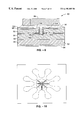
Both bottom-emitting and top-emitting VCSELs can be used for the transmitter modules via different packaging methods. FIG. 7 shows a schematic cross-section for a multiple-wavelength bottom-emitting VCSEL PIE array 40 formed on a substrate 42. A multimode fiber 44 with self-aligned Burrus-type [20] fiber-coupling configuration is attached to the substrate with epoxy 46. The substrate 42 of this embodiment is preferably comprised of the following series of layers: an AuGe/Ni/Au layer 48 for n-contact metallization, a GaAs substrate layer 50, an n-DBR layer 52, an active layer 54, a p-DBR layer 56, an insulating isolation layer 58, and a layer of Ti/Pt/Au 60 for contacting the p-DBR and for probing pads. Within this structure are shown an insulating, isolation layer 62 of, for example SiNx, and polyimide 64 wells and oxide apertures 66. FIG. 8 is a rendering of a scanning-electron micrograph (SEM) image of a finished bottom-emitting VCSEL PIE array which comprises eight “pie-shaped” VCSELs emitting eight different wavelengths. This structure corresponds to the configuration shown in FIG. 6. The exact number of elements in each array will be determined by the specific applications. However, the upper limit is usually set by processing techniques and device performance. Additionally, note that the “pie” shape is not essential. Other VCSEL shapes such as circles, triangles or squares may also be used as long as they fit within the circumference of the fiber core to which the VCSEL PIE array is to be attached.
Similarly, FIG. 9 and FIG. 10 illustrate the corresponding top-emitting approach. FIG. 9 shows a schematic cross-section for a proposed multiple-wavelength top-emitting VCSEL PIE array 80 formed on a substrate 82. A multimode fiber 84 is attached to the substrate with epoxy 86. The substrate 82 of this embodiment preferably comprises the following series of layers: an AuGe/Ni/Au layer 88 for n-contact metallization, a GaAs substrate layer 90, an n-DBR layer 92, an active layer 94, and a p-DBR 96, an insulating isolation layer 98, with a layer of Ti/Pt/Au 100 for contacting the p-DBR and for probing pads. Within this structure are shown a SiN x 102 anti-reflection coating and polyimide 104 wells along with oxide apertures 106.
FIG. 10 is a rendering of a scanning-electron micrograph (SEM) image of a finished top-emitting VCSEL PIE array which comprises eight VCSELs emitting eight different wavelengths. This metallization retains the previous “pie” structure yet employs circular contact areas.
The processing steps for the foregoing VCSEL PIE arrays is as follows. After epitaxial regrowth, the sample is patterned with photoresist for etching of the deep narrow trenches (3-5 μm wide) around the VCSELs for device isolation and access to the wet oxidation layer. As a result, arrays of eight pie-shaped VCSEL mesas were created after a pure C12 reactive-ion etching. These eight VCSELs are closely packed within a 60-μm-diameter circle to match the core of a multimode fiber. In order to avoid having an exposed Al0.9Gao.IAs layer at the bottom of the trenches, the first GaAs quarter-wave layer below the active region was designed with a thickness of 1.2 λ and the C12 etching was controlled to stop within this layer. After the trench etching, a short 2.5 minute wet oxidation process at 425° C. is performed to create an oxide aperture extending only 1.0 μm from the edge to facilitate multiple lateral-mode operation. Then the sample is covered with SiNX and the film on top of the VCSELs is removed by CF4/O2 plasma for Au/Zn/Au metallization.
FIG. 11 is a rendering of a scanning-electron micrograph (SEM) image 120 of the bottom-emitting VCSEL PIE array after the p-contact process. Before putting down the thick Ti/Pt/Au probing pads, the deep trenches 122, 124 are filled with polyimide for metal cross-over and isolation, respectively. The n-contact metallization on the substrate side of the sample is AuGe/Ni/Au. SiNx is used for anti-reflection coating on the bottom-emitting VCSELs. For the Burrus-type packaging scheme, an etching well is created in the substrate for self-aligned fiber coupling and also for better coupling efficiency.
FIG. 12A shows the experimental light-current curves for an eight-element bottom-emitting VCSEL PIE array with the design shown in FIG. 11 (m=4) but also with a 1.25-λ GaAs layer below the 1-λ cavity for the reason described earlier. FIG. 12B shows the corresponding experimental and theoretical threshold characteristics. Most devices lased at around 1.7 mA with a bias voltage of 2.4 V. If we number the devices according to the tuning layer thickness, channels #1 to #6 exhibit similar electrical and spectral characteristics when the output power is below 5 mW. Channel #4 has 7.3 mW maximum output power, 50.2% differential quantum efficiency, and 11.8% maximum wall-plug efficiency. As theoretically predicted, the device (channel #8) with a GaAs tuning layer over 1.0 λ lases at the adjacent higher-order mode. FIG. 12C shows the lasing spectra of this VCSEL PIE array measured at 5-6 mA. The achieved lasing wavelength span from this array is 32.9 nm, but the maximum available wavelength span is about 36.7 nm. From FIG. 12B one can see that only half of the usable tuning range has been used by this sample. It is possible to further optimize the channel allocation so that all eight channels can be located at the flat part of the threshold curve.
Similarly, FIG. 13A through FIG. 13C show the corresponding threshold characteristics and lasing spectra of the top-emitting VCSEL PIE arrays, respectively.
From the system point of view, the bottom-emitting VCSEL PIE scheme is preferred over the top-emitting version because the bottom-emitting version provides a larger emitting area for each array element which will, in turn, enhance the multimode operation that is recommended for multimode fiber systems [19]. Moreover, the bottom-emitting configuration is also compatible with the flip-chip bonding 20 as shown in FIG. 4 which provides adequate heat sinking for reducing thermal crosstalk between channels. However, the top-emitting VCSEL structure has the advantage of being able to monolithically integrate with wavelength-matched RCPD arrays, simply by etching off a few periods of the top DBR mirror of VCSELs which turns them into reasonably effective photodetectors [1], whose structure 140 is illustrated in FIG. 14. The structure shows both a dual-core multimode fiber 142 with a receiving fiber 144, and a transmission fiber 146. Both the receiving fiber 144 and transmission fiber 146 can be attached to the substrate 148 with its respective RCPDs 150 and VCSELs 152 in a single operation. In the embodiment shown, it is desirable to use the transparent indium-tin-oxide (ITO) top contact to avoid the difficulty in photolithographical alignment. In addition, sometimes it is also desirable to adapt the top-emitting scheme to avoid the substantial substrate absorption, such as 850 nm wavelength for GaAs substrates.
FIG. 15 gives theoretical design characteristics of the photodetector of FIG. 14. Both the 3 db optical bandwidth and the fraction of light absorbed are shown for a variable number of DBR panels in the top mirror.
Preliminary on-chip high-speed testing of the bottom-emitting VCSEL PIE arrays of the current embodiment, as in FIG. 7, has been performed using a modified coaxial probe [4]. Laser output was collected by a 62.5 μm-core graded-index fiber at the substrate side. FIG. 16A shows the typical modulation responses at various bias levels measured by a 20 GHz lightwave component analyzer. FIG. 16B shows the 3dB modulation bandwidth, f3dB, as a function of (I-Ith)½, where I is the bias current and Ith is the threshold current. The observed modulation current efficiency factor is 2.4 GHz/mA1/2, which is similar to that for a conventional 15 μm-diameter etched-post VCSEL which has about the same area as our “pie”-shape VCSEL (88λμm2). The RC-limited bandwidth of our devices is estimated to be around 6.5 GHz, which is close to what we have obtained. An additional proton implantation under the probing pads will be very helpful to reduce the parasitic capacitance. Data transmission through a 300m-long graded-index multimode fiber (with a 62.5-μm core diameter) has been performed by using an O/E converter as the receiver. The results show that these devices, designed without particular high-speed consideration, are already capable of transmitting data up to 1.5 Gb/sec/channel under a 223-1 pseudo-random bit sequence (PRBS) without error (<10-13 bit-error rate). Additional proton implantation or semi-insulating substrate approach will bring up the high-speed modulation performance at the expense of more complicated processing.
FIG. 17 shows an embodiment of a high-speed VCSEL PIE design 180 according to the invention. The die 182 contains a multimode fiber 184 of the self-aligned Burrus-type [20] fiber-coupling configuration attached to the substrate with epoxy 186. The integrated circuit die 182 of this embodiment comprises the following series of layers: an S.I. GaAs substrate layer 188, an i-DBR layer 190, an n-contact layer 192, an active layer 194, an H+implanted p-DBR layer 196, an insulating isolation layer 198, and a layer of Ti/Pt/Au 200 for contacting the unimplanted p-DBR and for probing pads. Within this structure are shown wells 202, 204 and 206 filled with polyimide for isolation and planarization, n- contacts 208, 210 comprising AuGe/Ni/Au, pcontacts 214, 216 comprising Pd/Zn/Au, and contact pads 200, 218 comprising Ti/Pt/Au. As it is illustrated, the p- contacts 214, 216 are on top of the VCSEL while the n- contacts 208, 210 have an intra-cavity configuration.
(b) RCPD receivers
For the direct-coupled WDM receiver designs according to the invention, RCPDs are also made in a circular device arrangement, just like the VCSEL PIE arrays, to facilitate broadcast-type wavelength demultiplexing. Therefore, when the optical fiber is aligned and slightly defocused to the center of the pie array, all eight elements will be equally illuminated with all input wavelengths, but each of them will only pick up the specific channel which lies within its absorption band. A splitting loss of 13 dB has been observed in this configuration at 1.55 μm with a single-mode fiber, which is close to the 11 dB theoretical value [9],[10]. Based on the same technology, we can also construct a WDM photodetector arrays at 0.98 μm in the InGaAs/AIGaAs/GaAs material system.
FIG. 18 shows a schematic cross-section of a bottom-illuminated multiple-channel resonant-cavity Schottky photodetector array 240. The die 242 contains a multimode fiber 244 of the self-aligned Burrus-type [20] fiber-coupling configuration attached to the substrate with epoxy 246. The integrated circuit die 242 of this embodiment comprises the following series of layers: an AuGeNi layer 247, a GaAs substrate layer 248, an AlGaAs/GaAs n-DBR layer 250, a residual absorber layer 252, a SiNx isolation layer 254, a contact pad metallization layer 256, an AuTiPtAu contact metallization 258, an AlGaAs tunable thickness cavity 260, and an absorber layer 262. The die structure 242 is attached to a submount 264 by means of solder pads 266 for electrical contacting and heat sinking.
FIG. 19 is a rendering of a scanning-electron micrograph (SEM) image of a finished eight-channel “pie”-shaped photodetector array for 0.98-μm WDM optical data links. These devices are narrow-band resonant-cavity Schottky photodiodes with the Schottky Au metal as the back mirror and the AlGaAs DBR as the front mirror. Cavity modes for the individual devices can be adjusted by performing anodic oxidation on the i-AIGaAs phase-tuning layers.
Schottky and P-i-N structures are the two common designs for high-performance photodiodes in either bottom-illuminating or top-illuminating configuration, which can be used to create narrow-band WDM resonant-cavity photodetectors.
FIG. 20 shows the refractive index profile 300 for a bottom-illuminated Schottky structure having a narrow-band RCPD design. The structure comprises a p-GaAs substrate 302, a front AlGaAs DBR 304, a GaAs cavity 306, a double GaAs QW absorber 308, a phase tuning layer 310, and an Au mirror 312.
FIG. 21 shows the profile 320 for a P-i-N structure with a few mirror periods on top to reduce the sensitivity to the tuning layer thickness. The structure comprises a substrate 322, a bottom (front) DBR composed of i-Al0.98Ga0.02As and Al0.32Ga0.68As layers 324, a Al0.32Ga0.6 8As cavity 326, a dual GaAs QW absorber 328, a few periods of back mirror 330, a phase tuning layer 332, an SiO2 isolation layer 334, and an Au layer 336 to complete the top (back) mirror.
The SiO2 layer in the P-i-N design is employed to prevent Au spiking into the lattice during contact annealing and to increase the back-mirror reflectivity. From the processing point of view, the Schottky structure is substantially simpler as the Schottky Au metal itself can be used as the back reflection mirror. However, the interface between the Au Schottky metal and the high Al-content semiconductor layer is not very stable. Degradation in photoresponse has been observed in previous In0.52Al0.48As/Au devices. Moreover, the photoresponse bandwidth has also been limited by the finite absorption in Au. Therefore, the alternative P-i-N solution becomes much more attractive. A novel P-i-N photodetector design is therefore proposed within the current invention which employs an anti-resonant oxide aperture.
FIG. 22 shows a device schematic for a P-i-N photodetector 360. The device comprises an S.I. GaAs substrate layer 362, a bottom DBR mirror 386, an i-GaAs cavity 366, an n+-GaAs bottom contact layer to which metal contacts 382 and 384 are applied, an InGaAs QW absorber 370, a p-DBR mirror stack 372, a p-GaAs tuning layer 374, a p-contact metal 376 enclosing a SiO2 layer 378 that isolates the contact from the optical mode, and an Au mirror 380. Underneath the ring p-contact 376, the Al0.98Gao.02As layers in the top DBR mirror 372 will be oxidized after the mesa etching to increase the DBR reflectivity to almost one. As a result, the undesired absorption underneath the ring p-contact which may cause line width broadening in the photoresponses can be eliminated over the whole channel span (−30 nm).
FIG. 23 shows the theoretical reflectivity spectra for positions under the Au back mirror 380 with tuning layer thicknesses of (solid curves, from left to right) 0.40, 0.50, and 0.62λ, respectively. The dashed curves are for positions under the ring p-contact 376 with the same tuning layer thicknesses. As can be seen, the undesired absorption outside the central SiO2/Au detection region has been significantly suppressed over the whole wavelength-tuning range of interest. However, the wavelength-tuning behavior for the P-i-N design is not linear, for the same reason described earlier in the VCSEL section.
FIG. 24 compares theoretical cavity-mode tuning characteristics for the bottom-illuminated Schottky and P-i-N photodetector designs shown in FIG. 18 and FIG. 22. In this calculation, the back DBR mirror for the P-i-N structure is assumed to be 0.5 period (solid curve, m=1) or 1.5 periods (dash-dotted curve, m=2) and the SiO2 layer is 100 nm.
In terms of photoresponse characteristics, it is very desirable to have passbands with flat tops and steep sides. A novel coupled-cavity structure has been proposed earlier to implement this requirement [11]. The idea is to add a low-loss cavity that is optically coupled to the absorptive cavity via an intermediate mirror.
FIG. 25 shows the refractive index profile 400 of a coupled-cavity Schottky photodiode design. The coupling of two cavities is desired to flatten the peak and steepen the sides of the photoresponse curve. The design comprises a GaAs substrate 402, a front (bottom) DBR mirror of GaAs/Al0.98Ga0.02As 404, a front GaAs cavity 406, a central coupling mirror of GaAs/Al0.92Ga0.08As 408, a dual InGaAs QW absorber 410, a back (top) GaAs cavity 412, a phase tuning layer 414, and an Au mirror 416. Preliminary experimental results clearly demonstrate the expected coupled-cavity effect. Modeling for an InGaAs/GaAs/AlGaAs design reveals that this new coupled-cavity structure will be able to show a 30-dB channel rejection ratio (in term of optical power) even when the optical channel spacing is as narrow as 1 nm. FIG. 26 shows a comparison of the theoretical reflectivity spectra for the single-cavity (both Schottky and P-i-N) and the coupled-cavity (Schottky) structures, where the absorption coefficient for at InGaAs QWs is assumed to be 1.0 μm−1.
Contrary to the demand for a high numerical aperture in the transmitter design to reduce modal noise effects, a large numerical aperture in optical fiber will significantly deteriorate the photodetector performance. FIG. 27 shows the angular variation of optical power absorption for incident planar waves of different wavelengths for the Schottky design shown in FIG. 18 with a normally-incident resonant wavelength of 978 nm. It can be seen from the graph, that the apparent resonant wavelength varies with the incident angle. This effect causes the photoresponse to broaden and thus limits the minimum channel spacing. Nevertheless, the problem is much more severe for the conventional discrete dielectric filter and photodetector approach. FIG. 28 shows a comparison of the angular variation of the resonant wavelength by using a resonantcavity photodetector (solid curve) or a SiO2/SiNX dielectric filter (dash curve) design. The resonant-cavity photodetector design can have either dielectric or semiconductor DBRs. As one can see, for the 62.5 μm-core fiber with a numerical aperture of 0.275, the resonant-cavity photodetector design can allow a much narrower channel spacing than the discrete dielectric filter approach.
Accordingly, a novel double-absorber design was described which avoids position sensitivity related to the cavity standing wave and eliminates the need for in-situ cavity-mode adjustment [12]. The idea is to set the center-to-center spacing of the two thin QW absorption layers at λ/4 so that the field2-absorption integral is independent of the position of the absorbers relative to the cavity standing wave. This is especially important within the disclosed embodiment as the cavity modes in an array will be varied over a wavelength span of around 30 nm, and it is crucial to maintain a reasonable balance between mirror reflections and cavity losses over the entire range in order to obtain a uniform photoresponse in each array. Moreover, in order to reduce crosstalk between channels, these devices are designed with a high-Q cavity by minimizing cavity losses and increasing cavity length to obtain narrow-band photoresponse. In addition, a novel coupled-cavity structure is proposed to achieve passbands with flat tops and steep sides to approach the ideal square-shape photoresponse and to ensure proper channel alignment [11]. Although the description above contains many specificities, these should not be construed as limiting the scope of the invention but as merely providing illustrations of some of the presently preferred embodiments of this invention.

Claims (11)

What is claimed is:
1. An optical data link, comprising:
(a) an array of vertical cavity surface emitting laser (VCSEL) emitters, operating at predetermined wavelengths, fabricated within a substrate configured for simultaneous direct coupling of the VCSEL array to an optical fiber;
(b) an optical fiber capable of communicating multiple optical wavelengths; and
(c) an array of optical detectors coupled to a terminating end of said optical fiber, wherein a set of reception wavelengths generally match the wavelengths transmitted by the optical VCSEL emitters such that multiple optical wavelengths can be simultaneously communicated at high-speed from the emitters to the detectors across the optical fiber.
2. An optical data link as recited in claim 1, wherein said VCSEL emitters are selected from the group consisting of bottom-emitting VCSEL emitters and top-emitting VCSEL emitters.
3. An optical data link as recited in claim 1, wherein said optical detectors comprise resonant cavity photodetectors having a double-absorber design with a field2-absorption integral that is independent of absorber position relative to the cavity standing wave, and wherein each said optical detector includes two thin quantum well absorption layers spaced apart at an approximate quarter-wavelength spacing.
4. An optical data link as recited in claim 1, wherein the VCSEL array is configured as a circular array of VCSEL emitters.
5. An optical data link as recited in claim 1, wherein the VCSEL array is configured with “pie-shaped” optical elements arranged in a circle.
6. An optical data link as recited in claim 1, wherein said optical fiber is coupled to said VCSEL array by the use of a self-aligned Burrus-type fiber-coupling configuration.
7. An optical data link as recited in claim 1, wherein said array of optical detectors comprises a resonant-cavity photodetector array directly coupled to the optical fiber.
8. An optical data link as recited in claim 1, wherein the VCSEL emitters are wavelength adjustable.
9. An optical data link comprising:
(a) an array of vertical cavity surface emitting laser (VCSEL) emitters configured for direct coupling to an optical fiber, wherein the VCSEL emitters operate at various predetermined emission wavelengths;
(b) an array of resonant cavity photodetector (RCPD) detectors configured for direct coupling to an optical fiber, said RCPD detectors having reception wavelengths generally corresponding to the emission wavelengths of the VCSEL emitters;
(c) an optical fiber directly coupled between the VCSEL emitter array and RCPD array, wherein multiple optical wavelengths can be simultaneously communicated at high-speed from the emitters to the detectors across the optical fiber.
10. An optical data link, as recited in claim 9, wherein the VCSEL emitters are wavelength adjustable.
11. A method of creating a multiple band optical link, comprising the steps of:
(a) fabricating a vertical cavity surface emitting laser (VCSEL) emitter array on a substrate, wherein the VCSEL emitters are arranged in a circular pattern on the substrate and each VCSEL emitter is set for a different emissive wavelength;
(b) configuring the substrate with the VCSEL emitters for Burrus-type selfaligning fiber-coupling;
(c) fabricating a resonant-cavity photodetector (RCPD) detector array on a substrate, wherein the RCPD detectors are arranged in a circular pattern on the substrate and each RCPD is set to detect a different emissive wavelength;
(d) configuring the substrate of the RCPD detector array for Burrus-type self-aligning fiber-coupling;
(e) bonding the substrates of the VCSEL emitter array and RCPD detector array onto electronic circuits configured to receive the respective emitter and detector arrays; and
(f) bonding a multi-mode fiber between the VCSEL emitter and RCPD detector, wherein said bonding is created by means of Burrus-style coupling.
US09/425,542 1998-10-26 1999-10-22 Direct-coupled multimode WDM optical data links with monolithically-integrated multiple-channel VCSEL and photodetector Expired - Lifetime US6195485B1 (en)

Priority Applications (2)

Application Number Priority Date Filing Date Title
US09/425,542 US6195485B1 (en) 1998-10-26 1999-10-22 Direct-coupled multimode WDM optical data links with monolithically-integrated multiple-channel VCSEL and photodetector
US09/738,162 US6574398B2 (en) 1998-10-26 2000-12-14 Direct-coupled multimode WDM optical data links with monolithically-integrated multiple-channel VCSEL and photodetector arrays

Applications Claiming Priority (2)

Application Number Priority Date Filing Date Title
US10570498P 1998-10-26 1998-10-26
US09/425,542 US6195485B1 (en) 1998-10-26 1999-10-22 Direct-coupled multimode WDM optical data links with monolithically-integrated multiple-channel VCSEL and photodetector

Related Child Applications (1)

Application Number Title Priority Date Filing Date
US09/738,162 Continuation US6574398B2 (en) 1998-10-26 2000-12-14 Direct-coupled multimode WDM optical data links with monolithically-integrated multiple-channel VCSEL and photodetector arrays

Publications (1)

Publication Number Publication Date
US6195485B1 true US6195485B1 (en) 2001-02-27

Family

ID=26802860

Family Applications (2)

Application Number Title Priority Date Filing Date
US09/425,542 Expired - Lifetime US6195485B1 (en) 1998-10-26 1999-10-22 Direct-coupled multimode WDM optical data links with monolithically-integrated multiple-channel VCSEL and photodetector
US09/738,162 Expired - Fee Related US6574398B2 (en) 1998-10-26 2000-12-14 Direct-coupled multimode WDM optical data links with monolithically-integrated multiple-channel VCSEL and photodetector arrays

Family Applications After (1)

Application Number Title Priority Date Filing Date
US09/738,162 Expired - Fee Related US6574398B2 (en) 1998-10-26 2000-12-14 Direct-coupled multimode WDM optical data links with monolithically-integrated multiple-channel VCSEL and photodetector arrays

Country Status (1)

Country Link
US (2) US6195485B1 (en)

Cited By (57)

* Cited by examiner, † Cited by third party
Publication number Priority date Publication date Assignee Title
US20020097771A1 (en) * 2000-12-06 2002-07-25 Wen-Yen Hwang Modified distributed bragg reflector (DBR) for vertical cavity surface-emitting laser (VCSEL) resonant wavelength tuning sensitivity control
US6493483B2 (en) 2000-12-13 2002-12-10 Bae Systems Information And Electronic System Integration Inc. Integrated circuit photonic signal matrix
US20030072053A1 (en) * 2001-10-11 2003-04-17 The Boeing Company Closed-loop optical network system and an associated transceiver and method for transmitting a plurality of optical signals
US6563185B2 (en) * 2001-05-21 2003-05-13 The Regents Of The University Of Colorado High speed electron tunneling device and applications
US20030133339A1 (en) * 2001-05-21 2003-07-17 Estes Michael J. Interconnected high speed electron tunneling devices
US20030156611A1 (en) * 2002-02-21 2003-08-21 Hoki Kwon GaAs/Al(Ga)As distributed bragg reflector on InP
US20030156610A1 (en) * 2002-02-21 2003-08-21 Hoki Kwon Carbon doped GaAsSb suitable for use in tunnel junctions of long-wavelength VCSELs
US6636544B2 (en) * 2000-12-06 2003-10-21 Applied Optoelectronics, Inc. Overlapping wavelength-tunable vertical cavity surface-emitting laser (VCSEL) arrays
US20030219917A1 (en) * 1998-12-21 2003-11-27 Johnson Ralph H. System and method using migration enhanced epitaxy for flattening active layers and the mechanical stabilization of quantum wells associated with vertical cavity surface emitting lasers
US6693934B2 (en) 2001-12-28 2004-02-17 Honeywell International Inc. Wavelength division multiplexed vertical cavity surface emitting laser array
US20040160997A1 (en) * 2003-02-15 2004-08-19 Peters Frank H. Frequency modulated vertical cavity laser
US20040165845A1 (en) * 2003-02-21 2004-08-26 Lemoff Brian E. Array of discretely formed optical signal emitters for multi-channel communication
US20040207926A1 (en) * 2002-02-22 2004-10-21 Buckman Lisa A. Structure and apparatus for a very short haul, free space, and fiber optic interconnect and data link
US20040228379A1 (en) * 2003-05-13 2004-11-18 Cox James A. VCSEL mode-transforming phase filter with enhanced performance
US6856749B2 (en) 2002-10-10 2005-02-15 Fitel Technologies, Inc. Optical coupling and alignment device
US6888863B1 (en) * 2000-06-30 2005-05-03 Lucent Technologies Inc. System comprising optical semiconductor waveguide device
US20050105578A1 (en) * 2003-11-17 2005-05-19 Alps Electric Co., Ltd. Wavelength-tunable light source and method for fabricating the same
US20050123015A1 (en) * 1998-12-21 2005-06-09 Johnson Ralph H. Use of GaAs extended barrier layers between active regions containing nitrogen and AlGaAs confining layers
US20050122880A1 (en) * 1999-08-19 2005-06-09 Hitachi, Ltd. Optical head with lasers and mirrors in a recess formed in a substrate
US20050129078A1 (en) * 1998-12-21 2005-06-16 Johnson Ralph H. Multicomponent barrier layers in quantum well active regions to enhance confinement and speed
GB2384617B (en) * 2001-10-15 2005-06-22 Arima Optoelectronic Semiconductor laser diodes
US20050157765A1 (en) * 1998-12-21 2005-07-21 Honeywell International Inc. Low temperature grown layers with migration enhanced epitaxy adjacent to an InGaAsN(Sb) based active region
US6922426B2 (en) 2001-12-20 2005-07-26 Finisar Corporation Vertical cavity surface emitting laser including indium in the active region
US20050180688A1 (en) * 2004-01-28 2005-08-18 Fuji Xerox Co., Ltd. Optical transmission device that employs vertical cavity surface-emitting laser diode as light source
US20050213983A1 (en) * 2004-03-25 2005-09-29 Shie Jin S Stack-integrated package of optical transceiver for single core full duplex fiber communications
US20050259916A1 (en) * 2003-05-21 2005-11-24 David Jenkins Multimode fiber optical fiber transmission system with offset launch single mode long wavelength vertical cavity surface emitting laser transmitter
US6975660B2 (en) 2001-12-27 2005-12-13 Finisar Corporation Vertical cavity surface emitting laser including indium and antimony in the active region
US20060012000A1 (en) * 2001-05-21 2006-01-19 Estes Michael J Thin-film transistors based on tunneling structures and applications
US20060038168A1 (en) * 2001-05-21 2006-02-23 Estes Michael J Terahertz interconnect system and applications
US20060091489A1 (en) * 2004-11-01 2006-05-04 International Business Machines Corporation Trench photodetector
US7058112B2 (en) 2001-12-27 2006-06-06 Finisar Corporation Indium free vertical cavity surface emitting laser
US7095770B2 (en) 2001-12-20 2006-08-22 Finisar Corporation Vertical cavity surface emitting laser including indium, antimony and nitrogen in the active region
US20060246700A1 (en) * 1998-12-21 2006-11-02 Johnson Ralph H Migration enhanced epitaxy fabrication of active regions having quantum wells
US20060267150A1 (en) * 2001-05-21 2006-11-30 Estes Michael J Metal-insulator varactor devices
US20070201525A1 (en) * 2004-10-01 2007-08-30 Finisar Corporation Vertical cavity surface emitting laser having strain reduced quantum wells
US20070274642A1 (en) * 2006-04-12 2007-11-29 Fujifilm Corporation Optical transmission system
EP1919046A2 (en) * 2006-09-28 2008-05-07 Fuji Xerox Co., Ltd. Surface-emitting semiconductor array device, module, light source device, data processing apparatus, light transmitting device, light spatial transmitting apparatus, and light spatial tansmitting system
US20080105820A1 (en) * 2006-11-07 2008-05-08 Cormack Robert H Resonant structures for electromagnetic energy detection system and associated methods
US20080131051A1 (en) * 2004-05-22 2008-06-05 Ocp-Europe, Ltd. Multi-mode fiber, optical fiber transmission system with offset-launch, single-mode, long-wavelength, vertical cavity surface emitting laser transmitter
US7408964B2 (en) 2001-12-20 2008-08-05 Finisar Corporation Vertical cavity surface emitting laser including indium and nitrogen in the active region
US20110090930A1 (en) * 2004-10-01 2011-04-21 Finisar Corporation Vertical cavity surface emitting laser with undoped top mirror
WO2011068492A1 (en) * 2009-12-03 2011-06-09 Moog Inc. Fiber optic rotary joints, methods practiced thereby, and fiber optic devices
WO2013104714A1 (en) * 2012-01-14 2013-07-18 Zinir Limited Light controller
EP2686924A2 (en) * 2011-03-17 2014-01-22 Finisar Corporation Lasers with quantum wells having high indium and low aluminum with barrier layers having high aluminum and low indium with reduced traps
US20140341590A1 (en) * 2013-05-15 2014-11-20 Hon Hai Precision Industry Co., Ltd. Optical communication device
CN104166189A (en) * 2013-05-16 2014-11-26 鸿富锦精密工业(深圳)有限公司 Optical communication apparatus
US9024297B2 (en) 2010-09-17 2015-05-05 The Governors Of The University Of Alberta Two- and three-terminal molecular electronic devices with ballistic electron transport
EP2808958A3 (en) * 2013-05-31 2015-05-20 Ricoh Company Ltd. Surface-Emitting Laser Element and Atomic Oscillator
US9178618B2 (en) 2013-10-22 2015-11-03 Globalfoundries Inc. Preassembled optoelectronic interconnect structure
US10020888B1 (en) * 2014-03-27 2018-07-10 Juniper Networks, Inc. Transmitter and receiver for direct communication of multiple optical wavelengths via an optical link
US20180233606A1 (en) * 2017-02-10 2018-08-16 Ciena Corporation Optically isolated photodiode for high sensitivity application
CN109579886A (en) * 2018-11-07 2019-04-05 桂林电子科技大学 A kind of high integration fibre optic interferometer
JP2020027147A (en) * 2018-08-10 2020-02-20 国立研究開発法人情報通信研究機構 Small optical transceiver
US20200321750A1 (en) * 2018-02-20 2020-10-08 Murata Manufacturing Co., Ltd. Light-emitting module
US11139635B2 (en) * 2018-06-19 2021-10-05 Excelitas Technologies Corp. Quantum well placement in a tunable VCSEL
US20210389242A1 (en) * 2018-07-13 2021-12-16 The Government Of The United States Of America, As Represented By The Secretary Of The Navy Highly Stable Semiconductor Lasers and Sensors for III-V and Silicon Photonic Integrated Circuits
US20220137230A1 (en) * 2020-10-30 2022-05-05 Waymo Llc Light Detection and Ranging (Lidar) Devices Having Vertical-Cavity Surface-Emitting Laser (VCSEL) Emitters

Families Citing this family (19)

* Cited by examiner, † Cited by third party
Publication number Priority date Publication date Assignee Title
US6920290B2 (en) * 2001-07-11 2005-07-19 Lockheed Martin Corporation Multi-wavelength high bandwidth communication receiver and system
US6829269B2 (en) 2002-05-21 2004-12-07 University Of Massachusetts Systems and methods using phonon mediated intersubband laser
US7004645B2 (en) * 2003-04-30 2006-02-28 Agilent Technologies, Inc. VCSEL array configuration for a parallel WDM transmitter
US7076129B2 (en) * 2003-04-30 2006-07-11 Lemoff Brian E Apparatus and method for a filterless parallel WDM multiplexer
US7412170B1 (en) * 2003-05-29 2008-08-12 Opticomp Corporation Broad temperature WDM transmitters and receivers for coarse wavelength division multiplexed (CWDM) fiber communication systems
JP4687064B2 (en) * 2004-10-22 2011-05-25 ソニー株式会社 Surface emitting semiconductor laser device
US7416352B2 (en) * 2005-09-08 2008-08-26 Northrop Grumman Corporation Optical multi-channel free space interconnect
US7873090B2 (en) * 2005-09-13 2011-01-18 Panasonic Corporation Surface emitting laser, photodetector and optical communication system using the same
US8089995B2 (en) * 2006-07-12 2012-01-03 Oracle America, Inc. Structures and methods for adjusting the wavelengths of lasers via temperature control
CN102136677B (en) * 2006-08-23 2015-06-17 株式会社理光 Surface-emitting laser array, optical scanning device, and image forming device
US7929865B2 (en) * 2007-07-27 2011-04-19 Hewlett-Packard Development Company, L.P. Free space WDM signal detector
US9429725B2 (en) 2013-04-19 2016-08-30 Avago Technologies General Ip (Singapore) Pte. Ltd. Bidirectional parallel optical transceiver module and a method for bidirectionally communicating optical signals over an optical link
US9323013B2 (en) 2013-04-19 2016-04-26 Avago Technologies General Ip (Singapore) Pte. Ltd. Bidirectional optical communications module having an optics system that reduces optical losses and increases tolerance to optical misalignment
US9531155B2 (en) * 2014-04-09 2016-12-27 Applied Optoelectronics, Inc. Switched radio frequency (RF) driver for tunable laser with multiple in-line sections
JP6743436B2 (en) * 2016-03-17 2020-08-19 株式会社リコー Surface emitting laser array and laser device
US10700780B2 (en) 2018-05-30 2020-06-30 Apple Inc. Systems and methods for adjusting movable lenses in directional free-space optical communication systems for portable electronic devices
US10705347B2 (en) 2018-05-30 2020-07-07 Apple Inc. Wafer-level high aspect ratio beam shaping
US11303355B2 (en) 2018-05-30 2022-04-12 Apple Inc. Optical structures in directional free-space optical communication systems for portable electronic devices
US11549799B2 (en) 2019-07-01 2023-01-10 Apple Inc. Self-mixing interference device for sensing applications

Citations (13)

* Cited by examiner, † Cited by third party
Publication number Priority date Publication date Assignee Title
US4773074A (en) 1987-02-02 1988-09-20 University Of Delaware Dual mode laser/detector diode for optical fiber transmission lines
US4948960A (en) 1988-09-20 1990-08-14 The University Of Delaware Dual mode light emitting diode/detector diode for optical fiber transmission lines
US5432630A (en) 1992-09-11 1995-07-11 Motorola, Inc. Optical bus with optical transceiver modules and method of manufacture
US5450508A (en) 1994-12-08 1995-09-12 International Business Machines Corporation Apparatus and method for optical fiber alignment using adaptive feedback control loop
US5532856A (en) 1994-06-30 1996-07-02 Nec Research Institute, Inc. Planar optical mesh-connected tree interconnect network
US5546209A (en) 1994-03-11 1996-08-13 University Of Southern California One-to-many simultaneous and reconfigurable optical two-dimensional plane interconnections using multiple wavelength, vertical cavity, surface-emitting lasers and wavelength-dependent detector planes
US5568574A (en) * 1995-06-12 1996-10-22 University Of Southern California Modulator-based photonic chip-to-chip interconnections for dense three-dimensional multichip module integration
US5633527A (en) 1995-02-06 1997-05-27 Sandia Corporation Unitary lens semiconductor device
US5671304A (en) 1995-12-21 1997-09-23 Universite Laval Two-dimensional optoelectronic tune-switch
US5678002A (en) 1995-07-18 1997-10-14 Microsoft Corporation System and method for providing automated customer support
US5684308A (en) 1996-02-15 1997-11-04 Sandia Corporation CMOS-compatible InP/InGaAs digital photoreceiver
US5724376A (en) * 1995-11-30 1998-03-03 Hewlett-Packard Company Transparent substrate vertical cavity surface emitting lasers fabricated by semiconductor wafer bonding
US6055262A (en) * 1997-06-11 2000-04-25 Honeywell Inc. Resonant reflector for improved optoelectronic device performance and enhanced applicability

Family Cites Families (5)

* Cited by examiner, † Cited by third party
Publication number Priority date Publication date Assignee Title
AU698782B2 (en) * 1995-09-29 1998-11-05 Ipg Photonics Corporation Optically resonant structure
US5768002A (en) 1996-05-06 1998-06-16 Puzey; Kenneth A. Light modulation system including a superconductive plate assembly for use in a data transmission scheme and method
US6128134A (en) * 1997-08-27 2000-10-03 Digital Optics Corporation Integrated beam shaper and use thereof
US6040590A (en) * 1996-12-12 2000-03-21 California Institute Of Technology Semiconductor device with electrostatic control
KR100413792B1 (en) * 1997-07-24 2004-02-14 삼성전자주식회사 Short wavelength surface emitting laser device including dbr having stacked structure of gan layer and air layer and fabricating method thereof

Patent Citations (14)

* Cited by examiner, † Cited by third party
Publication number Priority date Publication date Assignee Title
US4773074A (en) 1987-02-02 1988-09-20 University Of Delaware Dual mode laser/detector diode for optical fiber transmission lines
US4948960A (en) 1988-09-20 1990-08-14 The University Of Delaware Dual mode light emitting diode/detector diode for optical fiber transmission lines
US5432630A (en) 1992-09-11 1995-07-11 Motorola, Inc. Optical bus with optical transceiver modules and method of manufacture
US5546209A (en) 1994-03-11 1996-08-13 University Of Southern California One-to-many simultaneous and reconfigurable optical two-dimensional plane interconnections using multiple wavelength, vertical cavity, surface-emitting lasers and wavelength-dependent detector planes
US5532856A (en) 1994-06-30 1996-07-02 Nec Research Institute, Inc. Planar optical mesh-connected tree interconnect network
US5450508A (en) 1994-12-08 1995-09-12 International Business Machines Corporation Apparatus and method for optical fiber alignment using adaptive feedback control loop
US5633527A (en) 1995-02-06 1997-05-27 Sandia Corporation Unitary lens semiconductor device
US5568574A (en) * 1995-06-12 1996-10-22 University Of Southern California Modulator-based photonic chip-to-chip interconnections for dense three-dimensional multichip module integration
US5678002A (en) 1995-07-18 1997-10-14 Microsoft Corporation System and method for providing automated customer support
US5724376A (en) * 1995-11-30 1998-03-03 Hewlett-Packard Company Transparent substrate vertical cavity surface emitting lasers fabricated by semiconductor wafer bonding
US5837561A (en) * 1995-11-30 1998-11-17 Hewlett-Packard Company Fabrication of transparent substrate vertical cavity surface emitting lasers by semiconductor wafer bonding
US5671304A (en) 1995-12-21 1997-09-23 Universite Laval Two-dimensional optoelectronic tune-switch
US5684308A (en) 1996-02-15 1997-11-04 Sandia Corporation CMOS-compatible InP/InGaAs digital photoreceiver
US6055262A (en) * 1997-06-11 2000-04-25 Honeywell Inc. Resonant reflector for improved optoelectronic device performance and enhanced applicability

Non-Patent Citations (3)

* Cited by examiner, † Cited by third party
Title
Hu, S. et al., "1.55 micron pie-shaped resonant-cavity photodetector arrays for direct-coupled wavelength demultiplexing applications", Electrnic Letters Online No. 19970992, (2 pages), Jun. 25, 1997.
Hu, S. et al., "Coupled-cavity resonant photodetectors for high-performance wavelength demultiplexing applications", Applied Physics Letters, vol. 71, pp. 178-180, Jul. 14, 1997.
Hu, S. et al., "Resonant-cavity InGaAs/InAlGaAs/InP photodetector arrays for wavelenght demultiplexing applications", Applied Physics Letters, vol. 70, No. 18. pp. 2347-2349, May 5, 1997.

Cited By (105)

* Cited by examiner, † Cited by third party
Publication number Priority date Publication date Assignee Title
US20050129078A1 (en) * 1998-12-21 2005-06-16 Johnson Ralph H. Multicomponent barrier layers in quantum well active regions to enhance confinement and speed
US7435660B2 (en) 1998-12-21 2008-10-14 Finisar Corporation Migration enhanced epitaxy fabrication of active regions having quantum wells
US20060246700A1 (en) * 1998-12-21 2006-11-02 Johnson Ralph H Migration enhanced epitaxy fabrication of active regions having quantum wells
US7257143B2 (en) 1998-12-21 2007-08-14 Finisar Corporation Multicomponent barrier layers in quantum well active regions to enhance confinement and speed
US20050157765A1 (en) * 1998-12-21 2005-07-21 Honeywell International Inc. Low temperature grown layers with migration enhanced epitaxy adjacent to an InGaAsN(Sb) based active region
US20050142683A1 (en) * 1998-12-21 2005-06-30 Honeywell International System for developing a nitrogen-containing active region
US7167495B2 (en) 1998-12-21 2007-01-23 Finisar Corporation Use of GaAs extended barrier layers between active regions containing nitrogen and AlGaAs confining layers
US7378680B2 (en) 1998-12-21 2008-05-27 Finisar Corporation Migration enhanced epitaxy fabrication of quantum wells
US7286585B2 (en) 1998-12-21 2007-10-23 Finisar Corporation Low temperature grown layers with migration enhanced epitaxy adjacent to an InGaAsN(Sb) based active region
US20030219917A1 (en) * 1998-12-21 2003-11-27 Johnson Ralph H. System and method using migration enhanced epitaxy for flattening active layers and the mechanical stabilization of quantum wells associated with vertical cavity surface emitting lasers
US20050123015A1 (en) * 1998-12-21 2005-06-09 Johnson Ralph H. Use of GaAs extended barrier layers between active regions containing nitrogen and AlGaAs confining layers
US20050034661A1 (en) * 1998-12-21 2005-02-17 Finisar Corporation System for developing a nitrogen-containing active region
US7292519B2 (en) 1999-08-19 2007-11-06 Hitachi, Ltd. Optical head with lasers and mirrors in a recess formed in a substrate
US20050122880A1 (en) * 1999-08-19 2005-06-09 Hitachi, Ltd. Optical head with lasers and mirrors in a recess formed in a substrate
US6888863B1 (en) * 2000-06-30 2005-05-03 Lucent Technologies Inc. System comprising optical semiconductor waveguide device
US6724796B2 (en) * 2000-12-06 2004-04-20 Applied Optoelectronics, Inc. Modified distributed bragg reflector (DBR) for vertical cavity surface-emitting laser (VCSEL) resonant wavelength tuning sensitivity control
US20020097771A1 (en) * 2000-12-06 2002-07-25 Wen-Yen Hwang Modified distributed bragg reflector (DBR) for vertical cavity surface-emitting laser (VCSEL) resonant wavelength tuning sensitivity control
US6636544B2 (en) * 2000-12-06 2003-10-21 Applied Optoelectronics, Inc. Overlapping wavelength-tunable vertical cavity surface-emitting laser (VCSEL) arrays
US6493483B2 (en) 2000-12-13 2002-12-10 Bae Systems Information And Electronic System Integration Inc. Integrated circuit photonic signal matrix
US20070029544A1 (en) * 2001-05-21 2007-02-08 Estes Michael J Interconnected high speed electron tunneling devices
US20060012000A1 (en) * 2001-05-21 2006-01-19 Estes Michael J Thin-film transistors based on tunneling structures and applications
US7126151B2 (en) 2001-05-21 2006-10-24 The Regents Of The University Of Colorado, A Body Corporate Interconnected high speed electron tunneling devices
US7173275B2 (en) 2001-05-21 2007-02-06 Regents Of The University Of Colorado Thin-film transistors based on tunneling structures and applications
US7105852B2 (en) 2001-05-21 2006-09-12 University Technology Corporation High speed electron tunneling devices
US20040232505A1 (en) * 2001-05-21 2004-11-25 Garret Moddel High speed electron tunneling devices
US20060273301A1 (en) * 2001-05-21 2006-12-07 Garret Moddel High speed electron tunneling devices
US6756649B2 (en) 2001-05-21 2004-06-29 The Regents Of The University Of Colorado High speed electron tunneling device and applications
US7388276B2 (en) 2001-05-21 2008-06-17 The Regents Of The University Of Colorado Metal-insulator varactor devices
US20030133339A1 (en) * 2001-05-21 2003-07-17 Estes Michael J. Interconnected high speed electron tunneling devices
US20030127700A1 (en) * 2001-05-21 2003-07-10 Garret Moddel High speed electron tunneling device and applications
US20070120110A1 (en) * 2001-05-21 2007-05-31 Estes Michael J Thin-Film Transistors Based on Tunneling Structures and Applications
US7595500B2 (en) 2001-05-21 2009-09-29 University Technology Center Corp High speed electron tunneling devices
US20060267150A1 (en) * 2001-05-21 2006-11-30 Estes Michael J Metal-insulator varactor devices
US6563185B2 (en) * 2001-05-21 2003-05-13 The Regents Of The University Of Colorado High speed electron tunneling device and applications
US20060038168A1 (en) * 2001-05-21 2006-02-23 Estes Michael J Terahertz interconnect system and applications
US20030072053A1 (en) * 2001-10-11 2003-04-17 The Boeing Company Closed-loop optical network system and an associated transceiver and method for transmitting a plurality of optical signals
GB2384617B (en) * 2001-10-15 2005-06-22 Arima Optoelectronic Semiconductor laser diodes
US6922426B2 (en) 2001-12-20 2005-07-26 Finisar Corporation Vertical cavity surface emitting laser including indium in the active region
US7095770B2 (en) 2001-12-20 2006-08-22 Finisar Corporation Vertical cavity surface emitting laser including indium, antimony and nitrogen in the active region
US7408964B2 (en) 2001-12-20 2008-08-05 Finisar Corporation Vertical cavity surface emitting laser including indium and nitrogen in the active region
US6975660B2 (en) 2001-12-27 2005-12-13 Finisar Corporation Vertical cavity surface emitting laser including indium and antimony in the active region
US7058112B2 (en) 2001-12-27 2006-06-06 Finisar Corporation Indium free vertical cavity surface emitting laser
US6693934B2 (en) 2001-12-28 2004-02-17 Honeywell International Inc. Wavelength division multiplexed vertical cavity surface emitting laser array
US20030156611A1 (en) * 2002-02-21 2003-08-21 Hoki Kwon GaAs/Al(Ga)As distributed bragg reflector on InP
US6822995B2 (en) 2002-02-21 2004-11-23 Finisar Corporation GaAs/AI(Ga)As distributed bragg reflector on InP
US20030156610A1 (en) * 2002-02-21 2003-08-21 Hoki Kwon Carbon doped GaAsSb suitable for use in tunnel junctions of long-wavelength VCSELs
US7295586B2 (en) 2002-02-21 2007-11-13 Finisar Corporation Carbon doped GaAsSb suitable for use in tunnel junctions of long-wavelength VCSELs
US20040207926A1 (en) * 2002-02-22 2004-10-21 Buckman Lisa A. Structure and apparatus for a very short haul, free space, and fiber optic interconnect and data link
US7978981B2 (en) * 2002-02-22 2011-07-12 Avago Technologies Fiber Ip (Singapore) Pte. Ltd. Structure and apparatus for a very short haul, free space, and fiber optic interconnect and data link
US6856749B2 (en) 2002-10-10 2005-02-15 Fitel Technologies, Inc. Optical coupling and alignment device
US20040160997A1 (en) * 2003-02-15 2004-08-19 Peters Frank H. Frequency modulated vertical cavity laser
US7295589B2 (en) * 2003-02-15 2007-11-13 Avago Technologies Fiber (Singapore) Pte Ltd Frequency modulated vertical cavity laser
US6870195B2 (en) 2003-02-21 2005-03-22 Agilent Technologies, Inc. Array of discretely formed optical signal emitters for multi-channel communication
US20040165845A1 (en) * 2003-02-21 2004-08-26 Lemoff Brian E. Array of discretely formed optical signal emitters for multi-channel communication
US7061945B2 (en) 2003-05-13 2006-06-13 Finisar Corporation VCSEL mode-transforming phase filter with enhanced performance
US20040228379A1 (en) * 2003-05-13 2004-11-18 Cox James A. VCSEL mode-transforming phase filter with enhanced performance
US20050259916A1 (en) * 2003-05-21 2005-11-24 David Jenkins Multimode fiber optical fiber transmission system with offset launch single mode long wavelength vertical cavity surface emitting laser transmitter
US7231114B2 (en) 2003-05-21 2007-06-12 Ocp-Europe, Ltd. Multimode fiber optical fiber transmission system with offset launch single mode long wavelength vertical cavity surface emitting laser transmitter
US20050105578A1 (en) * 2003-11-17 2005-05-19 Alps Electric Co., Ltd. Wavelength-tunable light source and method for fabricating the same
US20050180688A1 (en) * 2004-01-28 2005-08-18 Fuji Xerox Co., Ltd. Optical transmission device that employs vertical cavity surface-emitting laser diode as light source
US7460749B2 (en) * 2004-01-28 2008-12-02 Fuji Xerox Co., Ltd. Optical transmission device that employs vertical cavity surface-emitting laser diode as light source
US20050213983A1 (en) * 2004-03-25 2005-09-29 Shie Jin S Stack-integrated package of optical transceiver for single core full duplex fiber communications
US7333684B2 (en) * 2004-03-25 2008-02-19 Integrated Crystal Technology Incorporated Stack-integrated package of optical transceiver for single core full duplex fiber communications
US7477815B2 (en) 2004-05-22 2009-01-13 Ocp-Europe, Ltd Multi-mode fiber, optical fiber transmission system with offset-launch, single-mode, long-wavelength, vertical cavity surface emitting laser transmitter
US20080131051A1 (en) * 2004-05-22 2008-06-05 Ocp-Europe, Ltd. Multi-mode fiber, optical fiber transmission system with offset-launch, single-mode, long-wavelength, vertical cavity surface emitting laser transmitter
US20070201525A1 (en) * 2004-10-01 2007-08-30 Finisar Corporation Vertical cavity surface emitting laser having strain reduced quantum wells
US8451875B2 (en) 2004-10-01 2013-05-28 Finisar Corporation Vertical cavity surface emitting laser having strain reduced quantum wells
US20110090930A1 (en) * 2004-10-01 2011-04-21 Finisar Corporation Vertical cavity surface emitting laser with undoped top mirror
US8168456B2 (en) 2004-10-01 2012-05-01 Finisar Corporation Vertical cavity surface emitting laser with undoped top mirror
US20070222015A1 (en) * 2004-11-01 2007-09-27 International Business Machines Corporation Trench photodetector
US7264982B2 (en) 2004-11-01 2007-09-04 International Business Machines Corporation Trench photodetector
US20060091489A1 (en) * 2004-11-01 2006-05-04 International Business Machines Corporation Trench photodetector
US20070274642A1 (en) * 2006-04-12 2007-11-29 Fujifilm Corporation Optical transmission system
EP1919046A2 (en) * 2006-09-28 2008-05-07 Fuji Xerox Co., Ltd. Surface-emitting semiconductor array device, module, light source device, data processing apparatus, light transmitting device, light spatial transmitting apparatus, and light spatial tansmitting system
EP1919046A3 (en) * 2006-09-28 2011-01-05 Fuji Xerox Co., Ltd. Surface-emitting semiconductor array device, module, light source device, data processing apparatus, light transmitting device, light spatial transmitting apparatus, and light spatial tansmitting system
US20080105820A1 (en) * 2006-11-07 2008-05-08 Cormack Robert H Resonant structures for electromagnetic energy detection system and associated methods
US9170378B2 (en) 2009-12-03 2015-10-27 Moog Inc. Fiber optic rotary joints, methods practiced thereby, and fiber optic devices
US9207406B2 (en) 2009-12-03 2015-12-08 Moog Inc. Fiber optic rotary joints, methods practiced thereby, and fiber optic devices
WO2011068492A1 (en) * 2009-12-03 2011-06-09 Moog Inc. Fiber optic rotary joints, methods practiced thereby, and fiber optic devices
US9024297B2 (en) 2010-09-17 2015-05-05 The Governors Of The University Of Alberta Two- and three-terminal molecular electronic devices with ballistic electron transport
EP2686924A2 (en) * 2011-03-17 2014-01-22 Finisar Corporation Lasers with quantum wells having high indium and low aluminum with barrier layers having high aluminum and low indium with reduced traps
EP2686924A4 (en) * 2011-03-17 2015-04-01 Finisar Corp Lasers with quantum wells having high indium and low aluminum with barrier layers having high aluminum and low indium with reduced traps
WO2013104714A1 (en) * 2012-01-14 2013-07-18 Zinir Limited Light controller
US20140341590A1 (en) * 2013-05-15 2014-11-20 Hon Hai Precision Industry Co., Ltd. Optical communication device
US9331787B2 (en) * 2013-05-15 2016-05-03 Hon Hai Precision Industry Co., Ltd. Optical communication device
CN104166189A (en) * 2013-05-16 2014-11-26 鸿富锦精密工业(深圳)有限公司 Optical communication apparatus
US9225149B2 (en) 2013-05-31 2015-12-29 Ricoh Company, Ltd. Surface emitting laser element and atomic oscillator
EP2808958A3 (en) * 2013-05-31 2015-05-20 Ricoh Company Ltd. Surface-Emitting Laser Element and Atomic Oscillator
US9178618B2 (en) 2013-10-22 2015-11-03 Globalfoundries Inc. Preassembled optoelectronic interconnect structure
US9490897B2 (en) 2013-10-22 2016-11-08 Globalfoundries Inc. Fabricating preassembled optoelectronic interconnect structures
US10020888B1 (en) * 2014-03-27 2018-07-10 Juniper Networks, Inc. Transmitter and receiver for direct communication of multiple optical wavelengths via an optical link
US20180233606A1 (en) * 2017-02-10 2018-08-16 Ciena Corporation Optically isolated photodiode for high sensitivity application
US10444445B2 (en) * 2017-02-10 2019-10-15 Ciena Corporation Optically isolated photodiode for high sensitivity application
US11799265B2 (en) * 2018-02-20 2023-10-24 Murata Manufacturing Co., Ltd. Light-emitting module
US20200321750A1 (en) * 2018-02-20 2020-10-08 Murata Manufacturing Co., Ltd. Light-emitting module
US11139635B2 (en) * 2018-06-19 2021-10-05 Excelitas Technologies Corp. Quantum well placement in a tunable VCSEL
US20210396669A1 (en) * 2018-07-13 2021-12-23 The Government Of The United States Of America, As Represented By The Secretary Of The Navy Highly Stable Semiconductor Lasers and Sensors for III-V and Silicon Photonic Integrated Circuits
US20210389242A1 (en) * 2018-07-13 2021-12-16 The Government Of The United States Of America, As Represented By The Secretary Of The Navy Highly Stable Semiconductor Lasers and Sensors for III-V and Silicon Photonic Integrated Circuits
US20210404957A1 (en) * 2018-07-13 2021-12-30 The Government Of The United States Of America, As Represented By The Secretary Of The Navy Highly Stable Semiconductor Lasers and Sensors for III-V and Silicon Photonic Integrated Circuits
US11709135B2 (en) * 2018-07-13 2023-07-25 The Government of the United States of America, as represented by the Secretary of the Naw Highly stable semiconductor lasers and sensors for III-V and silicon photonic integrated circuits
US11719633B2 (en) * 2018-07-13 2023-08-08 The Government Of The United States Of America, As Represented By The Secretary Of The Navy Highly stable semiconductor lasers and sensors for III-V and silicon photonic integrated circuits
US11761892B2 (en) * 2018-07-13 2023-09-19 The Government Of The United States Of America, As Represented By The Secretary Of The Navy Highly stable semiconductor lasers and sensors for III-V and silicon photonic integrated circuits
JP2020027147A (en) * 2018-08-10 2020-02-20 国立研究開発法人情報通信研究機構 Small optical transceiver
CN109579886A (en) * 2018-11-07 2019-04-05 桂林电子科技大学 A kind of high integration fibre optic interferometer
US20220137230A1 (en) * 2020-10-30 2022-05-05 Waymo Llc Light Detection and Ranging (Lidar) Devices Having Vertical-Cavity Surface-Emitting Laser (VCSEL) Emitters

Also Published As

Publication number Publication date
US20020009258A1 (en) 2002-01-24
US6574398B2 (en) 2003-06-03

Similar Documents

Publication Publication Date Title
US6195485B1 (en) Direct-coupled multimode WDM optical data links with monolithically-integrated multiple-channel VCSEL and photodetector
US6055262A (en) Resonant reflector for improved optoelectronic device performance and enhanced applicability
US7288421B2 (en) Method for forming an optoelectronic device having an isolation layer
US6836501B2 (en) Resonant reflector for increased wavelength and polarization control
US6148016A (en) Integrated semiconductor lasers and photodetectors
AU2006285426B2 (en) Optical phase conjugation laser diode
EP1352455B1 (en) Spatially modulated reflector for an optoelectronic device
US20040105476A1 (en) Planar waveguide surface emitting laser and photonic integrated circuit
WO2010091688A1 (en) Hybrid vertical-cavity laser
US8599897B2 (en) Tunable detector
US8532155B2 (en) Optical interconnection system
Hu et al. Multimode WDM optical data links with monolithically integrated multiple-channel VCSEL and photodetector arrays
Schnitzer et al. Biased and bias-free multi-Gb/s data links using GaAs VCSELs and 1300-nm single-mode fiber
CN110994358B (en) Electrically pumped tangential polarization vector beam laser
Hu et al. High-performance densely packed vertical-cavity photonic integrated emitter arrays for direct-coupled WDM applications
Chang-Hasnain VCSELs advances and future prospects
Sugihwo et al. Broadly-tunable narrow-linewidth micromachined laser/photodetector and phototransistor
Maier et al. Monolithic integration of vertical-cavity laser diodes and resonant photodetectors with hybrid Si 3 N 4-SiO 2 top Bragg mirrors
Coldren et al. Vertical-cavity surface-emitting lasers
Wipiejewski et al. 2D vertical-cavity laser arrays for free-space and multimode fiber transmission systems
Coldren et al. Research in Free-Space Interconnects Using Micro-Cavity Lasers

Legal Events

Date Code Title Description
AS Assignment

Owner name: REGENTS OF THE UNIVERSITY OF CALIFORNIA, THE, CALI

Free format text: ASSIGNMENT OF ASSIGNORS INTEREST;ASSIGNORS:COLDREN, LARRY A.;HU, SYN-YEM;REEL/FRAME:010504/0831;SIGNING DATES FROM 19991209 TO 19991213

STCF Information on status: patent grant

Free format text: PATENTED CASE

FEPP Fee payment procedure

Free format text: PAYER NUMBER DE-ASSIGNED (ORIGINAL EVENT CODE: RMPN); ENTITY STATUS OF PATENT OWNER: SMALL ENTITY

Free format text: PAYOR NUMBER ASSIGNED (ORIGINAL EVENT CODE: ASPN); ENTITY STATUS OF PATENT OWNER: SMALL ENTITY

FPAY Fee payment

Year of fee payment: 4

FPAY Fee payment

Year of fee payment: 8

REMI Maintenance fee reminder mailed
FPAY Fee payment

Year of fee payment: 12