US6211716B1 - Baseline wander compensation circuit and method - Google Patents

Baseline wander compensation circuit and method Download PDF

Info

Publication number
US6211716B1
US6211716B1 US09/322,247 US32224799A US6211716B1 US 6211716 B1 US6211716 B1 US 6211716B1 US 32224799 A US32224799 A US 32224799A US 6211716 B1 US6211716 B1 US 6211716B1
Authority
US
United States
Prior art keywords
signal
peak
forward path
coupled
stage
Prior art date
Legal status (The legal status is an assumption and is not a legal conclusion. Google has not performed a legal analysis and makes no representation as to the accuracy of the status listed.)
Expired - Lifetime
Application number
US09/322,247
Inventor
Hai T. Nguyen
Menping Chang
Current Assignee (The listed assignees may be inaccurate. Google has not performed a legal analysis and makes no representation or warranty as to the accuracy of the list.)
Microchip Technology Inc
Original Assignee
Kendin Communications Inc
Priority date (The priority date is an assumption and is not a legal conclusion. Google has not performed a legal analysis and makes no representation as to the accuracy of the date listed.)
Filing date
Publication date
Application filed by Kendin Communications Inc filed Critical Kendin Communications Inc
Priority to US09/322,247 priority Critical patent/US6211716B1/en
Assigned to KENDIN COMMUNICATIONS, INC. reassignment KENDIN COMMUNICATIONS, INC. ASSIGNMENT OF ASSIGNORS INTEREST (SEE DOCUMENT FOR DETAILS). Assignors: CHANG, MENPING, NGUYEN, HAI T.
Application granted granted Critical
Publication of US6211716B1 publication Critical patent/US6211716B1/en
Assigned to MICREL, INC. reassignment MICREL, INC. CONFIRMATORY ASSIGNMENT Assignors: KENDIN COMMUNICATIONS, INC.
Anticipated expiration legal-status Critical
Expired - Lifetime legal-status Critical Current

Links

Images

Classifications

    • HELECTRICITY
    • H03ELECTRONIC CIRCUITRY
    • H03FAMPLIFIERS
    • H03F3/00Amplifiers with only discharge tubes or only semiconductor devices as amplifying elements
    • H03F3/45Differential amplifiers
    • H03F3/45071Differential amplifiers with semiconductor devices only
    • H03F3/45479Differential amplifiers with semiconductor devices only characterised by the way of common mode signal rejection
    • H03F3/45928Differential amplifiers with semiconductor devices only characterised by the way of common mode signal rejection using IC blocks as the active amplifying circuit
    • H03F3/45968Differential amplifiers with semiconductor devices only characterised by the way of common mode signal rejection using IC blocks as the active amplifying circuit by offset reduction
    • H03F3/45973Differential amplifiers with semiconductor devices only characterised by the way of common mode signal rejection using IC blocks as the active amplifying circuit by offset reduction by using a feedback circuit
    • HELECTRICITY
    • H04ELECTRIC COMMUNICATION TECHNIQUE
    • H04LTRANSMISSION OF DIGITAL INFORMATION, e.g. TELEGRAPHIC COMMUNICATION
    • H04L25/00Baseband systems
    • H04L25/02Details ; arrangements for supplying electrical power along data transmission lines
    • H04L25/06Dc level restoring means; Bias distortion correction ; Decision circuits providing symbol by symbol detection
    • H04L25/061Dc level restoring means; Bias distortion correction ; Decision circuits providing symbol by symbol detection providing hard decisions only; arrangements for tracking or suppressing unwanted low frequency components, e.g. removal of dc offset
    • H04L25/063Setting decision thresholds using feedback techniques only
    • H04L25/064Subtraction of the threshold from the signal, which is then compared to a supplementary fixed threshold

Definitions

  • the present invention relates generally to the field of data communication and more particularly to a circuit and method for compensating for baseline wander occurrences in data signals.
  • a data signal is transmitted across a twisted-pair copper wire that is commonly known as CAT-5 cable.
  • the data signal is then AC coupled through a primary side of a transformer and received by a receiver connected to the secondary side of the transformer.
  • This method of AC coupling the data signals through the transformer may cause the average DC value of the signal to drift (i.e., wander) significantly over time, as shown in FIG. 1 a .
  • the data signal 100 is a waveform of an ideal MLT-3 signal, while the data signal 105 is a waveform of an MLT-3 signal that has been affected by Baseline Wander.
  • Baseline Wander occurs due to the high pass characteristics of the transformer.
  • the transformer will suppress the DC level if data signal remains in the same level for a long time. This can cause the data signals to “droop” over time, as illustrated in FIG. 1 a . This drooping behavior may accumulate over time and may cause a maximum offset of 750 mV, differentially.
  • Baseline Wander offset can cause serious signal distortions due to the limited linear range of the amplifiers along the data path and can cause high jitter. This makes data slicing difficult and results in received errors. Therefore, Baseline Wander correction is important in the recovery of transmitted data signals.
  • FIG. 1 b is a schematic block diagram of an offset cancellation circuit 120 , which includes a forward path block 121 with a gain of A 1 , feedback path block 122 with a feedback gain of A 2 , and a summing point 125 .
  • Equation (1) expresses the differential output voltage Vo of circuit 120 and explains the offset cancellation function.
  • V IN is the input signal in circuit 120 while ⁇ v is the offset voltage added to the input signal V IN .
  • equations (2) and (3) can then be subsequently derived from equation (1).
  • Vo (V IN + ⁇ v)A 1 /[1+(A 1 )(A 2 )] (3)
  • the feedback gain A 2 has a low pass characteristic such that it has a high gain (i.e., A 2 >>1) at low frequency operation and has a very small gain (i.e., A 2 ⁇ 1) at high frequency operation.
  • a 2 For a low frequency gain, A 2 >>1, the term [1+(A 1 ⁇ A 2 )] represents the denominator in the equation (3) and, therefore, the denominator also has a large value. As a result, the effect of offset is minimized.
  • the denominator of equation (3) approaches a unity value and equation (3) can be approximated as equation (4).
  • Vo (V IN + ⁇ v) ⁇ A 1 (4)
  • the offset voltage ⁇ v can not be canceled. Since the baseline wander effect is not a constant DC effect but an AC phenomenon, it is not cancelable by use of the offset cancellation circuit 120 .
  • a conventional Baseline Wander compensation version of an offset cancellation circuit 120 is shown in the circuit 150 of FIG. 1 c .
  • the circuit 150 includes a feed forward path block 121 with a gain of A 1 , the feedback path block 155 with a gain of A 2 and a summing point 125 .
  • the feedback path block 155 compares the output signal Vo with a replicated ideal signal 130 , which has the same DC bias, DC gain and AC gain as an ideal output signal Vo (ideal) with no Baseline Wander offset.
  • the feedback stage 155 detects this offset by comparing the output voltage Vo with the replica 130 and outputs a feedback signal 140 to compensate for Baseline Wander.
  • the offset or baseline wander is minimized at the input of the feed forward path block 121 .
  • phase difference there is a phase difference between the replica signal 130 and the output signal Vo, as shown in FIG. 1 d .
  • the effects of a phase difference can be “smoothed” out by using the low pass filter in the feedback path 155 , the phase difference still causes some unwanted ripple in the output signal 140 .
  • the data output Vo has excessive jitter (noise) due to the offset ripple into the summing point 125 and then amplified by 121 .
  • the apparatus and method of the present invention operates to track and dynamically compensate for the Baseline Wander event.
  • the apparatus includes a first peak detector for receiving a first signal from a forward path stage and capable of detecting a peak of the first signal, and a second peak detector for receiving a second signal from the forward path stage and capable of detecting a peak of the second signal.
  • the apparatus also includes a differential amplifier coupled to the first peak detector and the second peak detector and capable of generating an offset control signal, and a compensation stage coupled to the differential amplifier and capable of compensating for offset in the received signal in response to the offset control signal.
  • the apparatus may also include a pair of selective sample peak detectors that are capable of sampling a portion of the input signal.
  • the sampled portion of the input signal is defined by a “smart window” (timing window) which is received by a sample and block circuit of the peak detector.
  • a “smart window” timing window
  • the present invention is able to detect correctly the peak levels of the positive and negative signals independently and compares these levels for any potential offset caused by a Baseline Wander event.
  • the present invention then outputs a Baseline Wander control signal to compensate for Baseline Wander.
  • the method of Baseline Wander compensation in accordance with the present invention is able to compensate the offset in data signals independently of its AC and DC gain. Furthermore, the present invention provides a Baseline Wander compensation approach that is fully differential, thereby permitting a circuit in accordance with the present invention to have improved immunity to noise.
  • FIG. 1 a is a waveform diagram comparing an ideal MLT-3 signal with an MLT-3 signal affected by baseline wander;
  • FIG. 1 b is a schematic block diagram of a typical DC offset cancellation circuit
  • FIG. 1 c is a schematic block diagram of the conventional offset cancellation circuit by using a replicated signal
  • FIGS. 1 d - 1 e are waveform diagrams in the conventional circuit of FIG. 1 c ; they illustrate the phase and gain mismatches causing a ripple effect;
  • FIG. 2 a is a schematic block diagram of an offset or baseline wander compensation circuit in accordance with an embodiment of the present invention
  • FIG. 2 b is a schematic block diagram of the offset or baseline wander compensation circuit of FIG. 2 a shown in additional details;
  • FIG. 2 c is a waveform diagram that illustrates the conversion of data signals from MLT-3 into binary as triggers for the window generator
  • FIG. 2 d is a schematic block diagram of one embodiment of a smart window generator
  • FIG. 2 e illustrates the waveforms of the window generator in FIG. 2 d
  • FIG. 3 is a waveform diagram that shows the use of sampling windows to generate the average peak level of a signal
  • FIG. 4 a is a waveform diagram of data signals and their peaks before Baseline Wander compensation
  • FIG. 4 b is a waveform diagram of data signals and its peaks after Baseline Wander compensation
  • FIG. 5 is flowchart illustrating the operation of a baseline wander compensation circuit in accordance with an embodiment of the present invention.
  • FIG. 6 is an embodiment of the sample and block circuit coupled to the charge pump.
  • FIG. 2 a is a schematic block diagram of a circuit 200 for performing baseline wander and offset compensation, in accordance with an embodiment of the present invention.
  • the circuit 200 includes a forward path stage 202 for generating differential output signals P and M, peak detectors 204 a and 204 b for receiving the P signal and M signal, respectively, a differential amplifier 206 for comparing the outputs of peak detectors 204 a and 204 b , and a summing stage 207 to subtract the differential amplifier outputs from input signals 209 .
  • the circuit 200 applies a sampled peak detection approach to extract the peak levels of the signals P and M, as described in additional details below and in the above-referenced U.S. Application, filed May 28, 1999 Menping Chang and Hai T.
  • the peak detector 204 a or 204 b has a low-pass filter function, but with enough bandwidth to track the Baseline Wander event.
  • the present invention is able to detect and compensate the Baseline Wander offset dynamically. Therefore, the present invention advantageously does not rely on fixed amplitude signals or replica signal to compensate for Baseline Wander offset as required by the conventional approach.
  • FIG. 2 b is a schematic block diagram of the present invention shown in additional details that expand the peak detectors 204 a and 204 b into several components and introduces the additional circuit blocks, as described below, to correctly extract the peak information of the data signals P and M.
  • the comparators 215 a and 215 b compare the forward path 202 output signals P and M with an internal generated reference voltage Vref to slice out the output signals out_P and out_M, respectively. As shown in FIG. 2C, the MLT-3 data signal P is sliced against a voltage level Vref to generate output signal out_P, while the MLT-3 data signal M is sliced against a voltage level Vref to generate output signal out_M.
  • the circuit 200 also includes a pair of window generators 220 a and 220 b and a pair of peak detectors 204 a and 204 b . Similar window generators and peak detectors are also shown and described in the above-referenced U.S. Patent Application entitled “Selective Sampled Peak Detector” by Hai T. Nguyen and Menping Chang.
  • the pair of window generators 220 a and 220 b receives the output signals out_P and out_M, respectively, as triggers to generate timing control signals, 230 a and 230 b .
  • An example of such window generator is shown in the schematic block diagram of FIG. 2 d and the waveform for such a window generator is shown in FIG. 2 e .
  • the operation of the window generator is described as follows.
  • a signal out_P is delayed by a delay stage 260 by time ⁇ T and inverted by inverter 265 into an inverted/delayed signal out_P′.
  • the input signal out_P and the inverted/delay signal out_P′ are ANDed by AND gate 270 to generate the control signal 230 a.
  • the window generator 220 b outputs the control signal 230 b .
  • the timing control signals 230 a and 230 b are simply pulses with time interval ⁇ T.
  • the timing control signals 230 a and 230 b are then used as a timing windows to selectively “sample” the top peaks of the forward path output signals P and M through the peak detectors 204 a and 204 b , respectively.
  • the peak detector 204 a uses the timing control signal 230 a to “sample” the top peak of forward path output signal P to output the average top peak voltage P_top, while the peak detector 204 b uses the sample/block control signal 230 b to “sample” the top peak of forward path output signal M to output the average top peak voltage M_top.
  • the peak detector 204 a includes a comparator 240 for comparing the positive signal P with the average peak detector output P_top that is generated at the output of peak detector 204 a .
  • the comparator 240 generates a comparing value signal 242 based upon the comparison of the detected peak level of P signal (P_top) and the positive P signal.
  • a sample and block circuit 245 receives pulses 335 a - 335 c (FIG.
  • the charge pump 250 (FIG. 2 b ), which may include a pull-up current source 255 , a pull-down current source 260 , and a output capacitor 265 having a voltage value corresponding to P_top.
  • the charge pump 250 either charges up or charges down the capacitor 265 during ⁇ T time interval depending on whether the comparing value 242 is high or low, respectively.
  • the charge pump 250 is inactive outside the timing interval ⁇ T and the output voltage P_top remains the same during that time.
  • the output signal P_top averages out the top peaks 305 a - 305 c of signal P within the pulses 335 a - 335 c.
  • a differential amplifier 206 (FIG. 2 b ) then compares the values of the top peaks P_top and M_top for any potential offset caused by a Baseline Wander event and generates the compensation control signal 208 to the baseline wander compensation block 207 to compensate for BLW.
  • the top peaks P_top and M_top have the same voltage level if there is no offset or baseline wander event.
  • the offset starts to build up in the input signals 209 , in the forward path input signals 210 and consequently in the forward path output signals P and M.
  • the peak detectors 204 a and 204 b then track the peaks of output signals P and M with this offset.
  • the differential amplifier 206 sees this offset through the peak levels (P_top and M_top) and outputs the compensation control signals 208 to permit the baseline wander (BLW) compensation stage 207 to eliminate this offset by introducing a same amount of offset but in an opposite direction to the input signals 209 .
  • both output signals 210 of the baseline wander compensation (summing) stage 207 are balanced.
  • the output signals P and M and its top peaks P_top and M_top are also balanced.
  • FIG. 4 a illustrates the peak detector levels P_top and M_top of the MLT-3 signals P and M before Baseline Wander compensation is provided to the signals P and M.
  • FIG. 4 b illustrates the peak detector levels P_top and M_top of the MLT-3 signals P and M after Baseline Wander compensation is provided to the signals P and M.
  • the present invention eliminates the needs for a replica, stringent fixed amplitude and gain requirement of the data signals for the conventional approaches. Furthermore, the present invention can properly perform offset and baseline wander cancellation, even if the received signals are distorted due to overshoot and undershoot distortion. These distortions are either filtered out by the sampling window or averaged out by the peak detectors described above in present invention.
  • Another advantage achieved by the present invention is that it substantially reduces the circuit elements and complex algorithm implemented by generating the replica in the conventional approach, thereby reducing the operating current and die size.
  • the peak detectors and window generators discussed above are very small and simple building block.
  • the comparators, window generators and peak detectors in the present invention are existing circuit elements in the receiver block, which performs the equalized function and is described in the above-referenced U.S. Patent Application entitled “Adaptive Equalizer and Method” by Hai T. Nguyen and Menping Chang.
  • the present invention provides a baseline wander compensation approach that is fully differential, thereby permitting a circuit in accordance with the present invention to have improved immunity to noise.
  • the present invention also does not have the problem of the conventional circuit 160 of FIG. 1 d wherein a phase difference created between the data signal Vo and the replica signal 130 .
  • the present invention avoids the phase difference problem that can lead to improper baseline wander compensation and data recovery errors.
  • circuits 220 a and 220 b may be used to implement the circuits 220 a and 220 b for generating and controlling a smart window (FIG. 2 b ), depending on the application of the invention.
  • the implementation of circuits 220 a and 220 b may be varied, for example, to select a specific portion and/or pattern of pulses that is more meaningful for the applications.
  • the present invention has been described in considerable detail with the comparison of the top peaks of the data signals, other versions are possible.
  • the present invention may be set to track either the bottom peaks of the data signals or any voltage level extracted from the signals using the sampling window.
  • FIG. 5 is a flowchart 500 describing an operation of a baseline wander compensation circuit in accordance with the present invention.
  • a data signal is first received 505 by the baseline wander compensation circuit.
  • the pulse peaks of a positive signal P of the data signal and the pulse peaks of a negative signal M are then tracked 510 .
  • a comparison 515 is then made for the pulse peak values of the positive signal P and the negative signal M. Based on the comparison 515 , a proper amount of compensation can be determined 520 so that baseline wander or offset occurrence are eliminated from the data signal.
  • FIG. 6 is a schematic block diagram of an embodiment of a sample and block circuit 245 that is integrated with charge pump 250 . It is noted that other embodiments and configurations of the sample and block circuit 245 may be implemented depending on the application of the invention.
  • the smart windows 335 a - 335 c (FIG. 3) of signal 230 a control a pair of transmission gates 605 and 610 .
  • the gate 605 includes n-channel transistor 615 and p-channel transistor 620
  • the gate 610 includes n-channel transistor 625 and p-channel transistor 630 .
  • the comparing value signal 242 (from comparator 240 in FIG. 2 b ) is passed to pump control transistors 635 and 640 .
  • the pump control transistor 635 is on and the pump control transistor 640 is off, thereby permitting the charge pump 250 to pump up.
  • the pump control transistor 635 is off and the pump control transistor 640 is on, thereby permitting the charge pump 250 to pump down.
  • the pump-up current value I 1 is set by the fixed current source 255 including a current mirror formed by transistors 645 and 650 .
  • the pump-down current value I 2 is set by the fixed current source 260 including a current mirror formed by transistors 655 and 660 .
  • both transmission gates 605 and 610 are off.
  • the p-channel transistor 665 is on and will pull the gate of pump control transistor 635 high, thereby turning off transistor 635 .
  • the n-channel transistor 670 is on and pulls the gate of pump control transistor 640 low, thereby turning off the transistor 640 . Since the pump control transistors 635 and 640 are off, the value of I out is zero and the value of P_top remains the same.

Abstract

An apparatus of compensating for offset in a received signal generated from a forward path stage, includes a first peak detector for receiving a first signal from the forward path stage and capable of detecting a peak of the first signal; a second peak detector for receiving a second signal from the forward path stage and capable of detecting a peak of the second signal; a differential amplifier coupled to the first peak detector and the second peak detector and capable of generating an offset control signal; and a compensation stage coupled to the differential amplifier and capable of compensating for offset in the received signal in response to the offset control signal. A method of compensating for offset in a received signal includes detecting a level of a first signal from a forward path stage; detecting a level of a second signal from the forward path stage; and generating an offset control signal to reduce an offset in the received signal in response to the level difference of the first signal and the second signal.

Description

CROSS-REFERENCE TO RELATED APPLICATION
The subject matter of this application is related to the subject matter of the following co-pending U.S. Applications: (1) U.S. application Ser. No. 09/322,668, filed May 28, 1999 by Jung-Chen Lin, entitled “A DELAY LOCKED LOOP FOR SUB-MICRON SINGLE-POLY DIGITAL CMOS PROCESSES” which is fully incorporated herein by reference; (2) U.S. application Ser. No. 09/321,983, filed May 28, 1999 by Menping Chang and Vuong Kim Le, entitled “UNIVERSAL OUTPUT DRIVER AND FILTER” which is fully incorporated herein by reference; (3) U.S. application Ser. No. 09/321,403, filed May 28, 1999 by Menping Chang and Hai T. Nguyen, entitled “ADAPTIVE EQUALIZER AND METHOD” which is fully incorporated herein by reference; (4) U.S. application Ser. No. 09/321,935, filed May 28, 1999 by Menping Chang and Hai T. Nguyen, entitled “SELECTIVE SAMPLED PEAK DETECTOR AND METHOD” which is fully incorporated herein by reference.
FIELD OF THE INVENTION
The present invention relates generally to the field of data communication and more particularly to a circuit and method for compensating for baseline wander occurrences in data signals.
BACKGROUND OF THE INVENTION
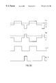
In 100 Base TX applications of a Copper Distributed Data Interface (CDDI), a data signal is transmitted across a twisted-pair copper wire that is commonly known as CAT-5 cable. The data signal is then AC coupled through a primary side of a transformer and received by a receiver connected to the secondary side of the transformer. This method of AC coupling the data signals through the transformer may cause the average DC value of the signal to drift (i.e., wander) significantly over time, as shown in FIG. 1a. The data signal 100 is a waveform of an ideal MLT-3 signal, while the data signal 105 is a waveform of an MLT-3 signal that has been affected by Baseline Wander.
Baseline Wander occurs due to the high pass characteristics of the transformer. The transformer will suppress the DC level if data signal remains in the same level for a long time. This can cause the data signals to “droop” over time, as illustrated in FIG. 1a. This drooping behavior may accumulate over time and may cause a maximum offset of 750 mV, differentially.
In the process of receiving and recovering data, uncompensated Baseline Wander offset can cause serious signal distortions due to the limited linear range of the amplifiers along the data path and can cause high jitter. This makes data slicing difficult and results in received errors. Therefore, Baseline Wander correction is important in the recovery of transmitted data signals.
An overview of a typical offset cancellation circuit is now discussed to provide better understanding of conventional approaches. FIG. 1b is a schematic block diagram of an offset cancellation circuit 120, which includes a forward path block 121 with a gain of A1, feedback path block 122 with a feedback gain of A2, and a summing point 125. Equation (1) expresses the differential output voltage Vo of circuit 120 and explains the offset cancellation function.
[(VIN+Δv)−(A2)(Vo)]A1=Vo  (1)
The term VIN is the input signal in circuit 120 while Δv is the offset voltage added to the input signal VIN. The equations (2) and (3) can then be subsequently derived from equation (1).
A1(VIN+Δv)=[1+(A1)(A2)]Vo  (2)
Vo=(VIN+Δv)A1/[1+(A1)(A2)]  (3)
For stability of the feedback system in FIG. 1b, the feedback gain A2 has a low pass characteristic such that it has a high gain (i.e., A2>>1) at low frequency operation and has a very small gain (i.e., A2<<1) at high frequency operation. For a low frequency gain, A2>>1, the term [1+(A1×A2)] represents the denominator in the equation (3) and, therefore, the denominator also has a large value. As a result, the effect of offset is minimized. However at high frequency, the denominator of equation (3) approaches a unity value and equation (3) can be approximated as equation (4).
Vo=(VIN+Δv)×A1  (4)
It is noted that in the case where equation (4) is satisfied, the offset voltage Δv can not be canceled. Since the baseline wander effect is not a constant DC effect but an AC phenomenon, it is not cancelable by use of the offset cancellation circuit 120.
A conventional Baseline Wander compensation version of an offset cancellation circuit 120 is shown in the circuit 150 of FIG. 1c. The circuit 150 includes a feed forward path block 121 with a gain of A1, the feedback path block 155 with a gain of A2 and a summing point 125. The feedback path block 155 compares the output signal Vo with a replicated ideal signal 130, which has the same DC bias, DC gain and AC gain as an ideal output signal Vo(ideal) with no Baseline Wander offset. As the Baseline Wander event occurs at the input signal VIN and consequentially at the output signal Vo, the feedback stage 155 detects this offset by comparing the output voltage Vo with the replica 130 and outputs a feedback signal 140 to compensate for Baseline Wander. As a result of this compensation, the offset or baseline wander is minimized at the input of the feed forward path block 121.
However in practice, there is a phase difference between the replica signal 130 and the output signal Vo, as shown in FIG. 1d. Although the effects of a phase difference can be “smoothed” out by using the low pass filter in the feedback path 155, the phase difference still causes some unwanted ripple in the output signal 140. As a result, the data output Vo has excessive jitter (noise) due to the offset ripple into the summing point 125 and then amplified by 121.
Another problem, which is more severe, is the variations and mismatches in either DC gain and AC gain of the output signal Vo and its ideal replica 130 as shown in FIG. 1e. Even though there is no phase shift in this case, the gain mismatch causes a residue signal that translates into offset ripple (Vo-Replica signal 130). Notice that Vo is the output of an analog signal and replica signal 130 is synthesized from a digital data. The two waveforms cannot be match perfectly in terms of overshoot and rise/fall time and it is very difficult for the forward block 121 to have a fix gain over process, temperature and supply voltage. This results in unwanted ripples and potential errors. These ripples are the results of phase delay and gain mismatch and are always present regardless of the effect of baseline wander. Consequently, the performance of this replica approach is very limited.
Therefore, there is a need for a baseline wander compensation approach that overcomes the unwanted ripples and errors in conventional baseline wander compensation systems.
SUMMARY OF THE INVENTION
The apparatus and method of the present invention operates to track and dynamically compensate for the Baseline Wander event. The apparatus includes a first peak detector for receiving a first signal from a forward path stage and capable of detecting a peak of the first signal, and a second peak detector for receiving a second signal from the forward path stage and capable of detecting a peak of the second signal. The apparatus also includes a differential amplifier coupled to the first peak detector and the second peak detector and capable of generating an offset control signal, and a compensation stage coupled to the differential amplifier and capable of compensating for offset in the received signal in response to the offset control signal.
In another aspect of the present invention, the apparatus may also include a pair of selective sample peak detectors that are capable of sampling a portion of the input signal. The sampled portion of the input signal is defined by a “smart window” (timing window) which is received by a sample and block circuit of the peak detector. By making uses of these peak detectors and the smart or timing windows, the present invention is able to detect correctly the peak levels of the positive and negative signals independently and compares these levels for any potential offset caused by a Baseline Wander event. The present invention then outputs a Baseline Wander control signal to compensate for Baseline Wander.
The method of Baseline Wander compensation in accordance with the present invention is able to compensate the offset in data signals independently of its AC and DC gain. Furthermore, the present invention provides a Baseline Wander compensation approach that is fully differential, thereby permitting a circuit in accordance with the present invention to have improved immunity to noise.
BRIEF DESCRIPTION OF THE DRAWINGS
FIG. 1a is a waveform diagram comparing an ideal MLT-3 signal with an MLT-3 signal affected by baseline wander;
FIG. 1b is a schematic block diagram of a typical DC offset cancellation circuit;
FIG. 1c is a schematic block diagram of the conventional offset cancellation circuit by using a replicated signal;
FIGS. 1d-1 e are waveform diagrams in the conventional circuit of FIG. 1c; they illustrate the phase and gain mismatches causing a ripple effect;
FIG. 2a is a schematic block diagram of an offset or baseline wander compensation circuit in accordance with an embodiment of the present invention;
FIG. 2b is a schematic block diagram of the offset or baseline wander compensation circuit of FIG. 2a shown in additional details;
FIG. 2c is a waveform diagram that illustrates the conversion of data signals from MLT-3 into binary as triggers for the window generator;
FIG. 2d is a schematic block diagram of one embodiment of a smart window generator;
FIG. 2e illustrates the waveforms of the window generator in FIG. 2d;
FIG. 3 is a waveform diagram that shows the use of sampling windows to generate the average peak level of a signal;
FIG. 4a is a waveform diagram of data signals and their peaks before Baseline Wander compensation;
FIG. 4b is a waveform diagram of data signals and its peaks after Baseline Wander compensation;
FIG. 5 is flowchart illustrating the operation of a baseline wander compensation circuit in accordance with an embodiment of the present invention; and
FIG. 6 is an embodiment of the sample and block circuit coupled to the charge pump.
DETAILED DESCRIPTION OF THE PREFERRED EMBODIMENTS
FIG. 2a is a schematic block diagram of a circuit 200 for performing baseline wander and offset compensation, in accordance with an embodiment of the present invention. The circuit 200 includes a forward path stage 202 for generating differential output signals P and M, peak detectors 204 a and 204 b for receiving the P signal and M signal, respectively, a differential amplifier 206 for comparing the outputs of peak detectors 204 a and 204 b, and a summing stage 207 to subtract the differential amplifier outputs from input signals 209. In one embodiment, the circuit 200 applies a sampled peak detection approach to extract the peak levels of the signals P and M, as described in additional details below and in the above-referenced U.S. Application, filed May 28, 1999 Menping Chang and Hai T. Nguyen, and entitled “SELECTIVE SAMPLED PEAK DETECTOR AND METHOD”. The peak detector 204 a or 204 b has a low-pass filter function, but with enough bandwidth to track the Baseline Wander event. By comparing the peak levels of signals P and M, the present invention is able to detect and compensate the Baseline Wander offset dynamically. Therefore, the present invention advantageously does not rely on fixed amplitude signals or replica signal to compensate for Baseline Wander offset as required by the conventional approach.
FIG. 2b is a schematic block diagram of the present invention shown in additional details that expand the peak detectors 204 a and 204 b into several components and introduces the additional circuit blocks, as described below, to correctly extract the peak information of the data signals P and M.
The comparators 215 a and 215 b compare the forward path 202 output signals P and M with an internal generated reference voltage Vref to slice out the output signals out_P and out_M, respectively. As shown in FIG. 2C, the MLT-3 data signal P is sliced against a voltage level Vref to generate output signal out_P, while the MLT-3 data signal M is sliced against a voltage level Vref to generate output signal out_M.
The circuit 200 also includes a pair of window generators 220 a and 220 b and a pair of peak detectors 204 a and 204 b. Similar window generators and peak detectors are also shown and described in the above-referenced U.S. Patent Application entitled “Selective Sampled Peak Detector” by Hai T. Nguyen and Menping Chang.
The pair of window generators 220 a and 220 b receives the output signals out_P and out_M, respectively, as triggers to generate timing control signals, 230 a and 230 b. An example of such window generator is shown in the schematic block diagram of FIG. 2d and the waveform for such a window generator is shown in FIG. 2e. The operation of the window generator is described as follows. A signal out_P is delayed by a delay stage 260 by time ΔT and inverted by inverter 265 into an inverted/delayed signal out_P′. The input signal out_P and the inverted/delay signal out_P′ are ANDed by AND gate 270 to generate the control signal 230 a.
Similarly for input signal out_M, the window generator 220 b outputs the control signal 230 b. As a result of using a window generator as shown in FIGS. 2d-2 e, the timing control signals 230 a and 230 b are simply pulses with time interval ΔT.
The timing control signals 230 a and 230 b are then used as a timing windows to selectively “sample” the top peaks of the forward path output signals P and M through the peak detectors 204 a and 204 b, respectively. The peak detector 204 a uses the timing control signal 230 a to “sample” the top peak of forward path output signal P to output the average top peak voltage P_top, while the peak detector 204 b uses the sample/block control signal 230 b to “sample” the top peak of forward path output signal M to output the average top peak voltage M_top.
Reference is now made to FIGS. 2b and 3 to describe the operation of a peak detector in FIG. 2b. In this example, only the operation of the peak detector 204 a is described. The peak detector 204 a includes a comparator 240 for comparing the positive signal P with the average peak detector output P_top that is generated at the output of peak detector 204 a. The comparator 240 generates a comparing value signal 242 based upon the comparison of the detected peak level of P signal (P_top) and the positive P signal. A sample and block circuit 245 receives pulses 335 a-335 c (FIG. 3) of time interval ΔT from the control signal 230 a, as sampling windows, to timely “ΔT” charge the charge pump 250 (FIG. 2b), which may include a pull-up current source 255, a pull-down current source 260, and a output capacitor 265 having a voltage value corresponding to P_top. The charge pump 250 either charges up or charges down the capacitor 265 during ΔT time interval depending on whether the comparing value 242 is high or low, respectively. The charge pump 250 is inactive outside the timing interval ΔT and the output voltage P_top remains the same during that time. As a result of selectively sampling the signal P by the peak detector, the output signal P_top averages out the top peaks 305 a-305 c of signal P within the pulses 335 a-335 c.
A differential amplifier 206 (FIG. 2b) then compares the values of the top peaks P_top and M_top for any potential offset caused by a Baseline Wander event and generates the compensation control signal 208 to the baseline wander compensation block 207 to compensate for BLW. The top peaks P_top and M_top have the same voltage level if there is no offset or baseline wander event.
As baseline wander occurs, the offset starts to build up in the input signals 209, in the forward path input signals 210 and consequently in the forward path output signals P and M. The peak detectors 204 a and 204 b then track the peaks of output signals P and M with this offset. The differential amplifier 206 sees this offset through the peak levels (P_top and M_top) and outputs the compensation control signals 208 to permit the baseline wander (BLW) compensation stage 207 to eliminate this offset by introducing a same amount of offset but in an opposite direction to the input signals 209. As a result, both output signals 210 of the baseline wander compensation (summing) stage 207 are balanced. Consequentially, the output signals P and M and its top peaks P_top and M_top are also balanced. The waveforms in FIG. 4a illustrate the peak detector levels P_top and M_top of the MLT-3 signals P and M before Baseline Wander compensation is provided to the signals P and M. FIG. 4b illustrates the peak detector levels P_top and M_top of the MLT-3 signals P and M after Baseline Wander compensation is provided to the signals P and M.
By using the peak detector approach to detect and compensate for baseline wander offset, the present invention eliminates the needs for a replica, stringent fixed amplitude and gain requirement of the data signals for the conventional approaches. Furthermore, the present invention can properly perform offset and baseline wander cancellation, even if the received signals are distorted due to overshoot and undershoot distortion. These distortions are either filtered out by the sampling window or averaged out by the peak detectors described above in present invention.
Another advantage achieved by the present invention is that it substantially reduces the circuit elements and complex algorithm implemented by generating the replica in the conventional approach, thereby reducing the operating current and die size. The peak detectors and window generators discussed above are very small and simple building block. In fact, the comparators, window generators and peak detectors in the present invention are existing circuit elements in the receiver block, which performs the equalized function and is described in the above-referenced U.S. Patent Application entitled “Adaptive Equalizer and Method” by Hai T. Nguyen and Menping Chang.
Additionally, the present invention provides a baseline wander compensation approach that is fully differential, thereby permitting a circuit in accordance with the present invention to have improved immunity to noise.
The present invention also does not have the problem of the conventional circuit 160 of FIG. 1d wherein a phase difference created between the data signal Vo and the replica signal 130. Thus, the present invention avoids the phase difference problem that can lead to improper baseline wander compensation and data recovery errors.
It is noted that other embodiments and configurations may be used to implement the circuits 220 a and 220 b for generating and controlling a smart window (FIG. 2b), depending on the application of the invention. The implementation of circuits 220 a and 220 b may be varied, for example, to select a specific portion and/or pattern of pulses that is more meaningful for the applications.
Although the present invention has been described in considerable detail with the comparison of the top peaks of the data signals, other versions are possible. For example, the present invention may be set to track either the bottom peaks of the data signals or any voltage level extracted from the signals using the sampling window.
FIG. 5 is a flowchart 500 describing an operation of a baseline wander compensation circuit in accordance with the present invention. A data signal is first received 505 by the baseline wander compensation circuit. The pulse peaks of a positive signal P of the data signal and the pulse peaks of a negative signal M are then tracked 510. A comparison 515 is then made for the pulse peak values of the positive signal P and the negative signal M. Based on the comparison 515, a proper amount of compensation can be determined 520 so that baseline wander or offset occurrence are eliminated from the data signal.
FIG. 6 is a schematic block diagram of an embodiment of a sample and block circuit 245 that is integrated with charge pump 250. It is noted that other embodiments and configurations of the sample and block circuit 245 may be implemented depending on the application of the invention. In the embodiment shown in FIG. 6, the smart windows 335 a-335 c (FIG. 3) of signal 230 a control a pair of transmission gates 605 and 610. The gate 605 includes n-channel transistor 615 and p-channel transistor 620, while the gate 610 includes n-channel transistor 625 and p-channel transistor 630. When the control signal 230 a is high (i.e., a smart window is high or asserted), the comparing value signal 242 (from comparator 240 in FIG. 2b) is passed to pump control transistors 635 and 640. Thus, if the comparing value signal 242 is high, then the pump control transistor 635 is on and the pump control transistor 640 is off, thereby permitting the charge pump 250 to pump up. If the comparing value signal 242 is low, then the pump control transistor 635 is off and the pump control transistor 640 is on, thereby permitting the charge pump 250 to pump down. The pump-up current value I1 is set by the fixed current source 255 including a current mirror formed by transistors 645 and 650. The pump-down current value I2 is set by the fixed current source 260 including a current mirror formed by transistors 655 and 660.
When the control signal 230 a is low (i.e., a smart window is not present), both transmission gates 605 and 610 are off. The p-channel transistor 665 is on and will pull the gate of pump control transistor 635 high, thereby turning off transistor 635. The n-channel transistor 670 is on and pulls the gate of pump control transistor 640 low, thereby turning off the transistor 640. Since the pump control transistors 635 and 640 are off, the value of Iout is zero and the value of P_top remains the same.

Claims (10)

What is claimed is:
1. An apparatus for compensating for offset and Baseline Wander Effect in an input signal, comprising:
a forward path stage configured to receive a forward path input signal and to generate a first forward path output signal (P) and a second forward path output signal (M);
coupled to the forward path stage, a first peak detector configured to receive the first forward path output signal (P) from the forward path stage and capable of detecting a peak of the first forward path output signal (P), the first peak detector further capable of generating a peak signal (P_top) which is a value of the peak of the first forward path output signal (P);
coupled to the forward path stage, a second peak detector configured to receive the second forward path output signal (M) from the forward path stage and capable of detecting a peak of the second forward path output signal (M), the second peak detector further capable of generating a peak signal (M_top) which is a value of the peak of the second forward path signal (M);
a first window generator coupled to the first peak detector and configured to generate a top peak timing window in response to a pulse occurrence in the first forward path output signal (P);
a second window generator coupled to the second peak detector and configured to generate a bottom peak timing window in response to a pulse occurrence in the second forward path output signal (M);
wherein the top peak timing window enables the first peak detector to process the first forward path output signal (P) to generate the peak signal (P_top);
wherein the bottom peak timing window enables the second peak detector to process the second forward path output signal (M) to generate the peak signal (M_top);
a differential amplifier coupled to the first peak detector and the second peak detector and capable of generating an offset control signal based upon a difference between the peak signal (P_top) and the peak signal (M_top); and
a compensation stage coupled to the differential amplifier and capable of compensating for offset in the input signal in response to the offset control signal, the compensation stage further configured to generate the forward path input signal for input into the forward path stage.
2. The apparatus of claim 1 wherein at least one of the peak detectors comprises:
a comparator having a first input for receiving one of the first forward path output signal (P) and the second forward path output signal (M), a second input for receiving a peak level signal of one of the first forward path output signal (P), and the second forward path output signal (M), and an output;
a sample and block circuit coupled to the output of the comparator and capable of sampling a portion of one of the first forward path output signal (P) and the second forward path output signal (M), the portion of one of the first forward path output signal (P) and the second forward path output signal (M) being defined by the timing window received by the sample and block circuit;
a charge pump coupled to the sample and block circuit and capable of setting a value of the peak level signal based upon a control signal generated by the sample and block circuit; and
a timing window generator coupled to the sample and block circuit and capable of generating the timing window.
3. The peak detector of claim 2 wherein the sample and block circuit comprises:
a first transmission gate capable of receiving the timing window;
a second transmission gate coupled to the first transmission gate and capable of receiving the timing window;
a first transistor coupled to the first transmission gate and capable generating a first output control signal having a value dependent on values of the input signal and the timing window; and
a second transistor coupled to the second transmission gate and capable of generating a second output control signal having a value dependent on values of the input signal and the timing window.
4. The peak detector of claim 2 wherein the timing window generator comprises:
a delay stage for receiving one of the first forward path output signal (P) and the second forward path output signal (M);
an inverter coupled to the delay stage and capable of generating an inverted signal; and
an AND gate coupled to the inverter and capable of receiving one of the first forward path output signal (P) and the second forward path output signal (M), and the inverted signal to generate a timing window.
5. A method of compensating for offset in an input signal, the method comprising:
receiving the input signal by use of a forward path stage, the input signal comprising a first signal (P) and a second signal (M);
detecting a level of the first signal (P);
detecting a level of the second signal (M);
generating a top peak timing window in response to a pulse occurrence in the first signal (P), wherein the top peak timing window enables processing of the first signal (P) to generate a peak signal (P_top) representing a level of the first signal (P);
generating a bottom peak timing window in response to a pulse occurrence in the second signal (M), wherein the bottom peak timing window enables processing of the second forward path output signal (M) to generate a peak signal (M_top) representing a level of the second signal (M); and
generating an offset control signal to reduce an offset in the input signal in response to a difference between the peak signal (P_top) and the peak signal (M_top).
6. An apparatus for compensating for offset occurrence in an input signal, comprising:
a summing stage configured to receive the input signal comprising a first signal (P) and a second signal (M);
coupled to the summing stage, a forward path stage configured to transmit the first signal (P) and the second signal (M);
coupled to the forward path stage, a first peak detector configured to detect a peak level of the first signal (P);
coupled to the forward path stage, a second peak detector configured to detect a peak level of the second signal (M);
a first window generator coupled to the first peak detector and configured to generate a top peak timing window in response to a pulse occurrence in the first signal (P);
a second window generator coupled to the second peak detector and configured to generate a bottom peak timing window in response to a pulse occurrence in the second signal (M);
wherein the top peak timing window enables the first peak detector to process the first signal (P) to determine the peak level of the first signal (P);
wherein the bottom peak timing window enables the second peak detector to process the second signal (M) to determine the peak level of the second signal (M); and
a differential amplifier for comparing the peak levels of the first signal (P) and the second signal (M) and for generating a compensation control signal based on the comparison of the peak levels, the compensation control signal permitting the summing stage to perform compensation on the input signal.
7. An apparatus for compensating for offset occurrence in an input signal, comprising:
a summing stage configured to receive the input signal including a first signal (P) and a second signal (M);
coupled to the summing stage, a forward path stage configured to transmit the first signal (P) and the second signal (M);
coupled to the forward path stage, first means for detecting a level of the first signal (P) from the forward path stage;
coupled to the forward path stage, second means for detecting a level of the second signal (M) from the forward path stage;
a first window generator coupled to the first means and configured to generate a top peak timing window in response to a pulse occurrence in the first signal (P);
a second window generator coupled to the second means and configured to generate a bottom peak timing window in response to a pulse occurrence in the second signal (M);
wherein the top peak timing window enables the first means to process the first signal (P) to generate the peak signal (P_top);
wherein the bottom peak timing window enables the second means to process the second forward path output signal (M) to generate the peak signal (M_top); and
coupled the first means and second means, means for generating an offset control signal to reduce an offset in the input signal in response to the level difference of the first signal (P) and the second signal (M), the summing stage providing compensation to the input signal in response to the control signal.
8. An apparatus for compensating for offset and Baseline Wander Effect in an input signal, comprising:
a forward path stage configured to receive a forward path input signal and to generate a first forward path output signal (P) and a second forward path output signal (M);
coupled to the forward path stage, a first peak detector configured to receive the first forward path output signal (P) from the forward path stage and capable of detecting a peak of the first forward path output signal (P), the first peak detector further capable of generating a peak signal (P_top) which is a value of the peak of the first forward path output signal (P);
coupled to the forward path stage, a second peak detector configured to receive the second forward path output signal (M) from the forward path stage and capable of detecting a peak of the second forward path output signal (M), the second peak detector further capable of generating a peak signal (M_top) which is a value of the peak of the second forward path signal (M);
a differential amplifier coupled to the first peak detector and the second peak detector and capable of generating an offset control signal based upon a difference between the peak signal (P_top) and the peak signal (M_top);
a compensation stage coupled to the differential amplifier and capable of compensating for offset in the input signal in response to the offset control signal, the compensation stage further configured to generate the forward path input signal for input into the forward path stage;
wherein at least one of the peak detectors comprises:
a comparator having a first input for receiving one of the first forward path output signal (P) and the second forward path output signal (M), a second input for receiving a peak level signal of one of the first forward path output signal (P), and the second forward path output signal (M), and an output;
a sample and block circuit coupled to the output of the comparator and capable of sampling a portion of one of the first forward path output signal (P), and the second forward path output signal (M), the portion of one of the first forward path output signal (P), and the second forward path output signal (M) being defined by a timing window received by the sample and block circuit;
a charge pump coupled to the sample and block circuit and capable of setting a value of the peak level signal based upon a control signal generated by the sample and block circuit; and
a timing window generator coupled to the sample and block circuit and capable of generating the timing window;
wherein the sample and block circuit comprises:
a first transmission gate capable of receiving the timing window;
a second transmission gate coupled to the first transmission gate and capable of receiving the timing window;
a first transistor coupled to the first transmission gate and capable generating a first output control signal having a value dependent on values of the input signal and the timing window; and
a second transistor coupled to the second transmission gate and capable of generating a second output control signal having a value dependent on values of the input signal and the timing window.
9. An apparatus for compensating for offset and Baseline Wander Effect in an input signal, comprising:
a forward path stage configured to receive a forward path input signal and to generate a first forward path output signal (P) and a second forward path output signal (M);
coupled to the forward path stage, a first peak detector configured to receive the first forward path output signal (P) from the forward path stage and capable of detecting a peak of the first forward path output signal (P), the first peak detector further capable of generating a peak signal (P_top) which is a value of the peak of the first forward path output signal (P);
coupled to the forward path stage, a second peak detector configured to receive the second forward path output signal (M) from the forward path stage and capable of detecting a peak of the second forward path output signal (M), the second peak detector further capable of generating a peak signal (M_top) which is a value of the peak of the second forward path signal (M);
a differential amplifier coupled to the first peak detector and the second peak detector and capable of generating an offset control signal based upon a difference between the peak signal (P_top) and the peak signal (M_top);
a compensation stage coupled to the differential amplifier and capable of compensating for offset in the input signal in response to the offset control signal, the compensation stage further configured to generate the forward path input signal for input into the forward path stage;
wherein at least one of the peak detectors comprises:
a comparator having a first input for receiving one of the first forward path output signal (P) and the second forward path output signal (M), a second input for receiving a peak level signal of one of the first forward path output signal (P) and the second forward path output signal (M), and an output;
a sample and block circuit coupled to the output of the comparator and capable of sampling a portion of one of the first forward path output signal (P) and the second forward path output signal (M), the portion of one of the first forward path output signal (P) and the second forward path output signal (M) being defined by a timing window received by the sample and block circuit;
a charge pump coupled to the sample and block circuit and capable of setting a value of the peak level signal based upon a control signal generated by the sample and block circuit;
a timing window generator coupled to the sample and block circuit and capable of generating the timing window;
wherein the timing window generator comprises:
a delay stage for receiving one of the first forward path output signal (P) and the second forward path output signal (M);
an inverter coupled to the delay stage and capable of generating an inverted signal; and
an AND gate coupled to the inverter and capable of receiving one of the first forward path output signal (P) and the second forward path output signal (M), and the inverted signal to generate a timing window.
10. An apparatus for compensating for offset occurrence in an input signal, comprising:
a summing stage configured to receive the input signal comprising a first signal (P) and a second signal (M);
coupled to the summing stage, a forward path stage configured to transmit the first signal (P) and the second signal (M);
coupled to the forward path stage, a first peak detector configured to detect a peak level of the first signal (P);
coupled to the forward path stage, a second peak detector configured to detect a peak level of the second signal (M);
a first window generator coupled to the first peak detector and configured to generate a top peak timing window in response to a pulse occurrence in the first signal (P);
a second window generator coupled to the second peak detector and configured to generate a bottom peak timing window in response to a pulse occurrence in the second signal (M);
wherein the top peak timing window enables the first peak detector to process the first signal (P) to determine the peak level of the first signal (P), the top peak timing window permitting the selective sampling of pulses of the first signal (P) to determine the peak level of the first signal (P);
wherein the bottom peak timing window enables the second peak detector to process the second signal (M) to determine the peak level of the second signal (M), the bottom peak timing window permitting the selective sampling of pulses of the second signal (M) to determine the peak level of the second signal (M); and
a differential amplifier for comparing the peak levels of the first signal (P) and the second signal (M) and for generating a compensation control signal based on the comparison of the peak levels, the compensation control signal permitting the summing stage to perform compensation on the input signal.
US09/322,247 1999-05-28 1999-05-28 Baseline wander compensation circuit and method Expired - Lifetime US6211716B1 (en)

Priority Applications (1)

Application Number Priority Date Filing Date Title
US09/322,247 US6211716B1 (en) 1999-05-28 1999-05-28 Baseline wander compensation circuit and method

Applications Claiming Priority (1)

Application Number Priority Date Filing Date Title
US09/322,247 US6211716B1 (en) 1999-05-28 1999-05-28 Baseline wander compensation circuit and method

Publications (1)

Publication Number Publication Date
US6211716B1 true US6211716B1 (en) 2001-04-03

Family

ID=23254043

Family Applications (1)

Application Number Title Priority Date Filing Date
US09/322,247 Expired - Lifetime US6211716B1 (en) 1999-05-28 1999-05-28 Baseline wander compensation circuit and method

Country Status (1)

Country Link
US (1) US6211716B1 (en)

Cited By (39)

* Cited by examiner, † Cited by third party
Publication number Priority date Publication date Assignee Title
US6385238B1 (en) * 1997-12-03 2002-05-07 Kabushiki Kaisha Toshiba Adaptive equalization and baseline wander correction circuit
US20020063937A1 (en) * 2000-11-29 2002-05-30 Osamu Kikuchi Optical receiving apparatus
US20020172295A1 (en) * 2001-05-15 2002-11-21 Dyer Kenneth C. Efficient, dynamically adaptive bias architecture and associated methods
WO2003047096A1 (en) * 2001-11-28 2003-06-05 Koninklijke Philips Electronics N.V. Compensation circuit for frequency filters
US6671075B1 (en) * 2002-06-24 2003-12-30 Oki Electric Industry Co., Ltd. Offset voltage cancellation circuit
US6674328B2 (en) * 2000-06-12 2004-01-06 Mitsubishi Denki Kabushiki Kaisha Amplifier circuit
US6690225B2 (en) * 2002-02-05 2004-02-10 Fujitsu Limited DC offset cancel circuit
US20040217780A1 (en) * 2002-01-07 2004-11-04 Fujitsu Limited DC component cancellation circuit
US6826390B1 (en) * 1999-07-14 2004-11-30 Fujitsu Limited Receiver, transceiver circuit, signal transmission method, and signal transmission system
US20040264582A1 (en) * 2003-06-30 2004-12-30 Intel Corporation Method for reducing DC offset error for single ended and differential signals
US20050285634A1 (en) * 2004-06-29 2005-12-29 Bruce Doyle Peak detector systems and methods with leakage compensation
US20060022719A1 (en) * 2004-07-27 2006-02-02 Hill Barrington J Peak detector
US20060255860A1 (en) * 2005-04-27 2006-11-16 Pmc-Sierra, Inc. Method and apparatus for detection of high-speed electrical signals
US20070030034A1 (en) * 2005-08-08 2007-02-08 Freescale Semiconductor Inc. Wide linear range peak detector
WO2007085870A1 (en) * 2006-01-24 2007-08-02 Future Waves Uk Limited A method of reducing d.c. offset
US7308057B1 (en) * 2003-06-05 2007-12-11 Maxtor Corporation Baseline wander compensation for perpendicular recording
US7330320B1 (en) * 2003-06-16 2008-02-12 Marvell International Ltd. Method and apparatus to limit DC-level in coded data
US20080061842A1 (en) * 2006-09-07 2008-03-13 Micron Technology, Inc. Circuit and method for detecting timed amplitude reduction of a signal relative to a threshold voltage
US20080063091A1 (en) * 2006-09-08 2008-03-13 Dong Yikui Jen AC coupling circuit integrated with receiver with hybrid stable common-mode voltage generation and baseline-wander compensation
US20080084956A1 (en) * 2006-09-18 2008-04-10 Milam Paraschou Absolute value peak differential voltage detector circuit and method
US20080157846A1 (en) * 2007-01-03 2008-07-03 Ren-Chieh Liu Dc offset calibration apparatus and method
US20080157847A1 (en) * 2007-01-03 2008-07-03 Ren-Chieh Liu Dc offset calibration apparatus and method for differential signals
US20080218890A1 (en) * 2007-03-07 2008-09-11 Rohm Co., Ltd. Baseline correction apparatus
US20090174449A1 (en) * 2008-01-03 2009-07-09 Bret Roberts Dale Driving circuit slew rate compensation method
US7649483B1 (en) 2000-05-23 2010-01-19 Marvell International Ltd. Communication driver
US20100074310A1 (en) * 2000-07-31 2010-03-25 Pierte Roo Active resistive summer for a transformer hybrid
US7729429B1 (en) 2000-05-23 2010-06-01 Marvell International Ltd. Active replica transformer hybrid
US7737788B1 (en) 2005-08-09 2010-06-15 Marvell International Ltd. Cascode gain boosting system and method for a transmitter
US7761076B1 (en) 2000-07-31 2010-07-20 Marvell International Ltd. Apparatus and method for converting single-ended signals to a differential signal, and transceiver employing same
USRE41831E1 (en) 2000-05-23 2010-10-19 Marvell International Ltd. Class B driver
US7853855B1 (en) 2005-08-25 2010-12-14 Marvell International Ltd. High speed iterative decoder
US20110050285A1 (en) * 2009-08-27 2011-03-03 Qualcomm Incorporated High linear fast peak detector
CN101430569B (en) * 2007-11-06 2011-03-30 瑞昱半导体股份有限公司 DC drift correction apparatus and method
US8050645B1 (en) 2000-07-31 2011-11-01 Marvell International Ltd. Active resistive summer for a transformer hybrid
US20120242327A1 (en) * 2011-03-24 2012-09-27 Lsi Corporation Fully differential signal peak detection architecture
US8493098B1 (en) * 2012-03-14 2013-07-23 Honeywell International Inc. Systems and methods for compensating the input offset voltage of a comparator
US20160013955A1 (en) * 2014-07-11 2016-01-14 Rambus Inc. On-Chip AC Coupled Receiver with Real-Time Linear Baseline-Wander Compensation
US10135644B1 (en) * 2017-08-31 2018-11-20 Qualcomm Incorporated Low power passive offset injection for 1-tap decision feedback equalizer
CN113497603A (en) * 2020-04-01 2021-10-12 智原微电子(苏州)有限公司 Device for baseline drift correction by means of differential drift current sensing

Citations (7)

* Cited by examiner, † Cited by third party
Publication number Priority date Publication date Assignee Title
US4575683A (en) * 1985-04-10 1986-03-11 Harris Corporation Apparatus and method for removing an offset signal
US5267269A (en) 1991-09-04 1993-11-30 Level One Communications, Inc. System and method employing predetermined waveforms for transmit equalization
US5428307A (en) * 1993-10-20 1995-06-27 Silicon Systems, Inc. Closed-loop peak detector topology
US5539779A (en) * 1993-04-20 1996-07-23 Nec Corporation Automatic offset control circuit for digital receiver
US5546027A (en) * 1994-12-12 1996-08-13 Silicon Systems, Inc. Peak detector
US6018407A (en) * 1996-05-20 2000-01-25 Nec Corporation Optical receiving circuit
US6041084A (en) * 1997-08-15 2000-03-21 Lucent Technologies, Inc. Circuit for optimal signal slicing in a binary receiver

Patent Citations (7)

* Cited by examiner, † Cited by third party
Publication number Priority date Publication date Assignee Title
US4575683A (en) * 1985-04-10 1986-03-11 Harris Corporation Apparatus and method for removing an offset signal
US5267269A (en) 1991-09-04 1993-11-30 Level One Communications, Inc. System and method employing predetermined waveforms for transmit equalization
US5539779A (en) * 1993-04-20 1996-07-23 Nec Corporation Automatic offset control circuit for digital receiver
US5428307A (en) * 1993-10-20 1995-06-27 Silicon Systems, Inc. Closed-loop peak detector topology
US5546027A (en) * 1994-12-12 1996-08-13 Silicon Systems, Inc. Peak detector
US6018407A (en) * 1996-05-20 2000-01-25 Nec Corporation Optical receiving circuit
US6041084A (en) * 1997-08-15 2000-03-21 Lucent Technologies, Inc. Circuit for optimal signal slicing in a binary receiver

Non-Patent Citations (3)

* Cited by examiner, † Cited by third party
Title
Everitt, James, et al., "A CMOS Transceiver for 10-Mb/s and 100-Mb/s Ethernet", Dec. 1998, pp. 2169-2177, IEEE Journal of Solid-State Circuits, vol. 33, No. 12.
Johnson, Mark G, et al. "A Variable Delay Line PLL for CPU-Coprocessor Synchronization" Oct. 1988, pp. 1218-1223, IEEE Journal of Solid-State Circuits, vol. 23 No. 5.
Sonntag, Jeff, et al. "A Monolithic CMOS 10 MHz DPLL for Burst-Mode Data Retiming", Feb. 16, 1990, pp. 194-195 and 294, 1990 IEEE International Solid-State Circuits Conference Digest of Technical Papers, 37th ISSCC, First Edition.

Cited By (76)

* Cited by examiner, † Cited by third party
Publication number Priority date Publication date Assignee Title
US6385238B1 (en) * 1997-12-03 2002-05-07 Kabushiki Kaisha Toshiba Adaptive equalization and baseline wander correction circuit
US7822403B2 (en) 1999-07-14 2010-10-26 Fujitsu Limited Receiver, transceiver circuit, signal transmission method, and signal transmission system
US20050033902A1 (en) * 1999-07-14 2005-02-10 Fujitsu Limited Receiver, transceiver circuit, signal transmission method, and signal transmission system
US7991359B2 (en) 1999-07-14 2011-08-02 Fujitsu Limited Receiver, transceiver circuit, signal transmission method, and signal transmission system
US20110012639A1 (en) * 1999-07-14 2011-01-20 Fujitsu Limited Receiver, transceiver circuit, signal transmission method, and signal transmission system
US20080242255A1 (en) * 1999-07-14 2008-10-02 Fujitsu Limited Receiver, transceiver circuit, signal transmission method, and signal transmission system
US7389097B2 (en) 1999-07-14 2008-06-17 Fujitsu Limited Receiver, transceiver circuit, signal transmission method, and signal transmission system
US6826390B1 (en) * 1999-07-14 2004-11-30 Fujitsu Limited Receiver, transceiver circuit, signal transmission method, and signal transmission system
USRE41831E1 (en) 2000-05-23 2010-10-19 Marvell International Ltd. Class B driver
US7804904B1 (en) 2000-05-23 2010-09-28 Marvell International Ltd. Active replica transformer hybrid
US7729429B1 (en) 2000-05-23 2010-06-01 Marvell International Ltd. Active replica transformer hybrid
US8009073B2 (en) 2000-05-23 2011-08-30 Marvell International Ltd. Method and apparatus for generating an analog signal having a pre-determined pattern
US20100127909A1 (en) * 2000-05-23 2010-05-27 Sehat Sutardja Communication driver
US7649483B1 (en) 2000-05-23 2010-01-19 Marvell International Ltd. Communication driver
US6674328B2 (en) * 2000-06-12 2004-01-06 Mitsubishi Denki Kabushiki Kaisha Amplifier circuit
US8050645B1 (en) 2000-07-31 2011-11-01 Marvell International Ltd. Active resistive summer for a transformer hybrid
US8503961B1 (en) 2000-07-31 2013-08-06 Marvell International Ltd. Active resistive summer for a transformer hybrid
US20100074310A1 (en) * 2000-07-31 2010-03-25 Pierte Roo Active resistive summer for a transformer hybrid
US7761076B1 (en) 2000-07-31 2010-07-20 Marvell International Ltd. Apparatus and method for converting single-ended signals to a differential signal, and transceiver employing same
US8880017B1 (en) 2000-07-31 2014-11-04 Marvell International Ltd. Active resistive summer for a transformer hybrid
US8045946B2 (en) 2000-07-31 2011-10-25 Marvell International Ltd. Active resistive summer for a transformer hybrid
US20020063937A1 (en) * 2000-11-29 2002-05-30 Osamu Kikuchi Optical receiving apparatus
US20020172295A1 (en) * 2001-05-15 2002-11-21 Dyer Kenneth C. Efficient, dynamically adaptive bias architecture and associated methods
US6845132B2 (en) * 2001-05-15 2005-01-18 Intel Corporation Efficient, dynamically adaptive bias architecture and associated methods
WO2003047096A1 (en) * 2001-11-28 2003-06-05 Koninklijke Philips Electronics N.V. Compensation circuit for frequency filters
US20040217780A1 (en) * 2002-01-07 2004-11-04 Fujitsu Limited DC component cancellation circuit
US6690225B2 (en) * 2002-02-05 2004-02-10 Fujitsu Limited DC offset cancel circuit
US6671075B1 (en) * 2002-06-24 2003-12-30 Oki Electric Industry Co., Ltd. Offset voltage cancellation circuit
US7308057B1 (en) * 2003-06-05 2007-12-11 Maxtor Corporation Baseline wander compensation for perpendicular recording
US7330320B1 (en) * 2003-06-16 2008-02-12 Marvell International Ltd. Method and apparatus to limit DC-level in coded data
US8773786B1 (en) 2003-06-16 2014-07-08 Marvell International Ltd. System for correcting DC characteristics of a magnetic recording system
US8358479B1 (en) * 2003-06-16 2013-01-22 Marvell International Ltd. Method and apparatus to limit DC-level in coded data
US9165599B1 (en) 2003-06-16 2015-10-20 Marvell International Ltd. Method for correcting DC characteristics in a magnetic recording system
US8098447B1 (en) * 2003-06-16 2012-01-17 Marvell International Ltd. Method and apparatus to limit DC-level in coded data
US7583456B1 (en) 2003-06-16 2009-09-01 Marvell International Ltd. Method and apparatus to limit DC-level in coded data
US7379511B2 (en) * 2003-06-30 2008-05-27 Intel Corporation Method for reducing DC offset error for single ended and differential signals
US20040264582A1 (en) * 2003-06-30 2004-12-30 Intel Corporation Method for reducing DC offset error for single ended and differential signals
US20050285634A1 (en) * 2004-06-29 2005-12-29 Bruce Doyle Peak detector systems and methods with leakage compensation
US7135892B2 (en) * 2004-06-29 2006-11-14 Hewlett-Packard Development Company, L.P. Peak detector systems and methods with leakage compensation
US7180335B2 (en) * 2004-07-27 2007-02-20 Facility Monitoring Systems Limited Peak detector
US20060022719A1 (en) * 2004-07-27 2006-02-02 Hill Barrington J Peak detector
US7348808B2 (en) * 2005-04-27 2008-03-25 Pmc-Sierra, Inc. Method and apparatus for detection of high-speed electrical signals
US20060255860A1 (en) * 2005-04-27 2006-11-16 Pmc-Sierra, Inc. Method and apparatus for detection of high-speed electrical signals
US7355456B2 (en) * 2005-08-08 2008-04-08 Freescale Semiconductor, Inc. Wide linear range peak detector
US20070030034A1 (en) * 2005-08-08 2007-02-08 Freescale Semiconductor Inc. Wide linear range peak detector
US7737788B1 (en) 2005-08-09 2010-06-15 Marvell International Ltd. Cascode gain boosting system and method for a transmitter
US7853855B1 (en) 2005-08-25 2010-12-14 Marvell International Ltd. High speed iterative decoder
US8175208B2 (en) 2006-01-24 2012-05-08 Future Waves Uk Limited Method of reducing d.c. offset
US20100166114A1 (en) * 2006-01-24 2010-07-01 Future Waves Uk Limited Method of reducing d.c. offset
WO2007085870A1 (en) * 2006-01-24 2007-08-02 Future Waves Uk Limited A method of reducing d.c. offset
US20080061842A1 (en) * 2006-09-07 2008-03-13 Micron Technology, Inc. Circuit and method for detecting timed amplitude reduction of a signal relative to a threshold voltage
US20080063091A1 (en) * 2006-09-08 2008-03-13 Dong Yikui Jen AC coupling circuit integrated with receiver with hybrid stable common-mode voltage generation and baseline-wander compensation
US7961817B2 (en) 2006-09-08 2011-06-14 Lsi Corporation AC coupling circuit integrated with receiver with hybrid stable common-mode voltage generation and baseline wander compensation
US20080084956A1 (en) * 2006-09-18 2008-04-10 Milam Paraschou Absolute value peak differential voltage detector circuit and method
US7560959B2 (en) * 2006-09-18 2009-07-14 Micron Technology, Inc. Absolute value peak differential voltage detector circuit and method
US20080157846A1 (en) * 2007-01-03 2008-07-03 Ren-Chieh Liu Dc offset calibration apparatus and method
US20080157847A1 (en) * 2007-01-03 2008-07-03 Ren-Chieh Liu Dc offset calibration apparatus and method for differential signals
US7777546B2 (en) 2007-01-03 2010-08-17 Realtek Semiconductor Corp. DC offset calibration apparatus and method for differential signals
US7612600B2 (en) * 2007-01-03 2009-11-03 Realtek Semiconductor Corp. DC offset calibration apparatus and method
US20080218890A1 (en) * 2007-03-07 2008-09-11 Rohm Co., Ltd. Baseline correction apparatus
US7889446B2 (en) * 2007-03-07 2011-02-15 Rohm Co., Ltd. Baseline correction apparatus
CN101430569B (en) * 2007-11-06 2011-03-30 瑞昱半导体股份有限公司 DC drift correction apparatus and method
US20090174449A1 (en) * 2008-01-03 2009-07-09 Bret Roberts Dale Driving circuit slew rate compensation method
US7663418B2 (en) * 2008-01-03 2010-02-16 Nanya Technology Corp. Driving circuit slew rate compensation method
US20110050285A1 (en) * 2009-08-27 2011-03-03 Qualcomm Incorporated High linear fast peak detector
US8310277B2 (en) * 2009-08-27 2012-11-13 Qualcomm, Incorporated High linear fast peak detector
US20120242327A1 (en) * 2011-03-24 2012-09-27 Lsi Corporation Fully differential signal peak detection architecture
US8791691B2 (en) * 2011-03-24 2014-07-29 Lsi Corporation Fully differential signal peak detection architecture
US8736312B2 (en) 2012-03-14 2014-05-27 Honeywell International Inc. Systems and methods for compensating the input offset voltage of a comparator
US8493098B1 (en) * 2012-03-14 2013-07-23 Honeywell International Inc. Systems and methods for compensating the input offset voltage of a comparator
US20160013955A1 (en) * 2014-07-11 2016-01-14 Rambus Inc. On-Chip AC Coupled Receiver with Real-Time Linear Baseline-Wander Compensation
US9491008B2 (en) * 2014-07-11 2016-11-08 Rambus Inc. On-chip AC coupled receiver with real-time linear baseline-wander compensation
US9794088B2 (en) 2014-07-11 2017-10-17 Rambus Inc. On-chip AC coupled receiver with real-time linear baseline-wander compensation
US10135644B1 (en) * 2017-08-31 2018-11-20 Qualcomm Incorporated Low power passive offset injection for 1-tap decision feedback equalizer
CN113497603A (en) * 2020-04-01 2021-10-12 智原微电子(苏州)有限公司 Device for baseline drift correction by means of differential drift current sensing
CN113497603B (en) * 2020-04-01 2023-09-19 智原微电子(苏州)有限公司 Device for baseline wander correction by means of differential wander current sensing

Similar Documents

Publication Publication Date Title
US6211716B1 (en) Baseline wander compensation circuit and method
US7496161B2 (en) Adaptive equalization system for a signal receiver
US5426389A (en) System for DC restoration of serially transmitted binary signals
US5614855A (en) Delay-locked loop
US9438450B1 (en) Receiver and associated control method
US8565296B2 (en) Adaptive receiver system and adaptive transceiver system
US9401800B1 (en) Clock data recovery system for Serdes
US6356160B1 (en) Phase lock loop and automatic gain control circuitry for clock recovery
US6140857A (en) Method and apparatus for reducing baseline wander
US4520489A (en) Decision feedback equalizing apparatus
US20060088089A1 (en) Adaptive equalizer with dual loop adaptation mechanism
US20050238092A1 (en) Method and system for error estimation for adaptive equalization in communication systems
US5963606A (en) Phase error cancellation method and apparatus for high performance data recovery
US20050135510A1 (en) Decision feedback equalizer and clock and data recovery circuit for high speed applications
EP0687398B1 (en) Receive side pulse width controlled adaptive equalizer
KR102584020B1 (en) Compensation of common mode voltage drop at sense amplifier output due to decision feedback equalizer (DFE) taps
US6114882A (en) Current comparator and method therefor
US5930302A (en) Balanced phase data bus transmitter
US6975678B1 (en) Apparatus and averaging method for equalizing signals
US4423518A (en) Timing recovery circuit
US6650720B1 (en) Phase lock loop and transconductance circuit for clock recovery
EP1545044A2 (en) Decision feedback equalizer and clock and data recovery circuit for high-speed applications
EP1145426B1 (en) Data pulse receiver
US5502746A (en) Dual stage differential adaptive peak detector for data communications receivers
CA2356242C (en) Pll and gain control for clock recovery

Legal Events

Date Code Title Description
AS Assignment

Owner name: KENDIN COMMUNICATIONS, INC., CALIFORNIA

Free format text: ASSIGNMENT OF ASSIGNORS INTEREST;ASSIGNORS:NGUYEN, HAI T.;CHANG, MENPING;REEL/FRAME:010208/0159

Effective date: 19990728

FEPP Fee payment procedure

Free format text: PAT HLDR NO LONGER CLAIMS SMALL ENT STAT AS NONPROFIT ORG (ORIGINAL EVENT CODE: LSM3); ENTITY STATUS OF PATENT OWNER: LARGE ENTITY

STCF Information on status: patent grant

Free format text: PATENTED CASE

AS Assignment

Owner name: MICREL, INC., CALIFORNIA

Free format text: CONFIRMATORY ASSIGNMENT;ASSIGNOR:KENDIN COMMUNICATIONS, INC.;REEL/FRAME:013117/0508

Effective date: 20020712

FPAY Fee payment

Year of fee payment: 4

FPAY Fee payment

Year of fee payment: 8

FPAY Fee payment

Year of fee payment: 12